US6389566B1 - Edge-triggered scan flip-flop and one-pass scan synthesis methodology - Google Patents
Edge-triggered scan flip-flop and one-pass scan synthesis methodologyDownload PDFInfo
- Publication number
- US6389566B1 US6389566B1US09/088,754US8875498AUS6389566B1US 6389566 B1US6389566 B1US 6389566B1US 8875498 AUS8875498 AUS 8875498AUS 6389566 B1US6389566 B1US 6389566B1
- Authority
- US
- United States
- Prior art keywords
- scan
- signal
- input
- output
- data
- Prior art date
- Legal status (The legal status is an assumption and is not a legal conclusion. Google has not performed a legal analysis and makes no representation as to the accuracy of the status listed.)
- Expired - Lifetime
Links
- 238000000034methodMethods0.000titleclaimsabstractdescription20
- 230000015572biosynthetic processEffects0.000titleabstractdescription6
- 238000003786synthesis reactionMethods0.000titleabstractdescription5
- 230000001960triggered effectEffects0.000titledescription6
- 238000012360testing methodMethods0.000claimsdescription52
- 238000012546transferMethods0.000claimsdescription32
- 238000013461designMethods0.000claimsdescription14
- 230000000295complement effectEffects0.000claimsdescription9
- 238000013507mappingMethods0.000claimsdescription7
- 230000008859changeEffects0.000claimsdescription5
- 230000006870functionEffects0.000claimsdescription2
- 230000008569processEffects0.000abstractdescription7
- 238000012938design processMethods0.000abstractdescription4
- 238000010586diagramMethods0.000description11
- 230000007704transitionEffects0.000description6
- 230000000630rising effectEffects0.000description5
- 230000003247decreasing effectEffects0.000description4
- 238000012986modificationMethods0.000description2
- 230000004048modificationEffects0.000description2
- 230000000644propagated effectEffects0.000description2
- 238000001308synthesis methodMethods0.000description2
- 230000006399behaviorEffects0.000description1
- 230000003111delayed effectEffects0.000description1
- 230000000694effectsEffects0.000description1
- 230000003116impacting effectEffects0.000description1
- 238000005457optimizationMethods0.000description1
- 230000004044responseEffects0.000description1
Images


Classifications
- G—PHYSICS
- G01—MEASURING; TESTING
- G01R—MEASURING ELECTRIC VARIABLES; MEASURING MAGNETIC VARIABLES
- G01R31/00—Arrangements for testing electric properties; Arrangements for locating electric faults; Arrangements for electrical testing characterised by what is being tested not provided for elsewhere
- G01R31/28—Testing of electronic circuits, e.g. by signal tracer
- G01R31/317—Testing of digital circuits
- G01R31/3181—Functional testing
- G01R31/3185—Reconfiguring for testing, e.g. LSSD, partitioning
- G01R31/318533—Reconfiguring for testing, e.g. LSSD, partitioning using scanning techniques, e.g. LSSD, Boundary Scan, JTAG
- G01R31/318541—Scan latches or cell details
Definitions
- This inventionrelates generally to the design of digital integrated circuits, and more specifically to an improved edge-triggered scan flip-flop and one-pass scan synthesis method.
- every possible combination of inputs to an integrated circuitis applied when the integrated circuit is in every possible internal logic state, thus allowing every possible output of the circuit to be compared with the functional requirements of the circuit.
- a combinational circuitwhich is a circuit in which the outputs of the circuit depend directly on the inputs to the circuit, and which thereby does not contain memory elements
- the number of possible input combinationsis sufficiently large that the test of the circuit becomes an NP hard problem, that is one that cannot be solved in polynomial time.
- a sequential circuitwhich is a circuit that contains internal memory and thus may have a number of internal logic states, the problem of testing every conceivable input combination in every combination of logic states of the circuit becomes even more intractable.
- testing of the circuit by manipulating the primary inputs and examining the primary outputsprovides little information as to a location of a fault within the circuit.
- the knowledge that a certain combination of inputs to a circuit results in an incorrect combination of outputs from the circuitmay be of little use in determining where in the circuit the error occurs.
- a scan flip-flopmay be used as a control point for inserting a value into a circuit, or as an observation point for observing a value at a point in the circuit.
- Scan flip-flopsare generally tied, or stitched, together to form a scan chain, with the scan chain forming a serial shift register. Data may be shifted in to provide input values for the circuit, or shifted out to capture the state of a portion of the circuit.
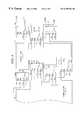
- FIG. 1illustrates a digital logic circuit.
- the digital logic circuitincludes combinational circuit elements 11 , 13 .
- Scan flip-flops 15 A-Gare dispersed about the combinational circuit elements 11 , 13 .
- Each of the scan flip-flops 15 A-Ghas four input ports for receiving associated input signals and one output port for outputting an associated output signal.
- the input portsare a data-in input port (D IN ), a scan-in input port (S IN ), a clock input port (CLK), and a test mode signal input port ( ⁇ overscore (N) ⁇ /T).
- Each of the scan flip-flopshas a single data-out output port (Q).
- the output Qis set to D IN after the rising edge of the clock signal when the test mode signal is set to a ⁇ overscore (TEST) ⁇ value.
- TEST⁇ overscore
- the scan flip-flopacts as an edge-triggered flip-flop.
- the output signal Qis set to S IN after the rising edge of the clock signal.
- the scan flip-flopsare edge-triggered flip-flops made scannable by adding a scan input and a multiplexer with an associated control signal.
- the scan flip-flops 15 A-Gare formed into a serial scan chain, i.e., a serial shift register, by connecting the Q data output of one scan flip-flop to the S IN port of another scan flip-flop. Accordingly, in addition to connecting the Q data output 19 A of scan flip-flop 15 A to the combinational circuit 13 , the Q data output 19 A is also connected to the S IN scan input port of scan flip-flop 15 B.
- the Q data output 19 Bis connected to the S IN input port of scan flip-flop 15 C
- the Q data output 19 Cis connected to the S IN input port of scan flip-flop 15 D
- the Q data output 19 Dis connected to the S IN input port of scan flip-flop 15 E
- the Q data output 19 Eis connected to the S IN input port of scan flip-flop 15 F
- the Q data output 19 Eis connected to the S IN input port of scan flip-flop 15 G.
- the S IN input 20 to scan flip-flop 15 Ais accessible by a circuit tester
- the Q data output 19 G of scan flip-flop 15 Gis readable by the circuit tester. Accordingly, the scannable flip-flops 15 A-G are stitched together to form a serial chain in the order of 15 A- 15 B- 15 C- 15 D- 15 E- 15 F- 15 G.
- the scan flip-flopsact both as control points and observation points.
- Control pointsmay be treated as pseudo-primary inputs (PIs) and observation points may be treated as pseudo-primary outputs (POs).
- PIspseudo-primary inputs
- POspseudo-primary outputs
- the scan flip-flops 15 A-Gare first treated as pseudo-PIs and are provided an input test vector comprised of state bits.
- the input test vectoris provided by setting the test mode signal to ⁇ overscore (TEST) ⁇ and sequentially placing input data on the S IN line 20 every clock cycle. The first clock cycle after the input data is placed on the S IN line shifts the input data to the S IN input of the next scan flip-flop in the scan chain.
- each of the scan flip-flops in the scan chainmay be loaded with a state bit from the test vector.
- setting the test mode signal to ⁇ overscore (TEST) ⁇allows for normal circuit operation, with the circuit utilizing the data input to the scan flip-flops as pseudo-primary outputs.
- the test mode signalis again set to ⁇ overscore (TEST) ⁇ .
- providing clock signals to the circuitcauses the data present on the output ports of the scan flip-flops to be sequentially shifted to the next scan flip-flop in the scan chain, with the data being read from output 19 G by a tester.
- Proper operation of the scan chaintherefore generally requires that the scan shift chain operate in a race-free manner. If a race condition exists then the data in the scan chain may be corrupted and provide either an incorrect test vector or an incorrect indication of system state. For example, during a scan data shift operation an edge of the clock signal may reach scan flip-flop 15 D a period of time prior to the edge of the clock signal reaching scan flip-flop 15 E. If the period of time is sufficiently long, the input to the scan flip-flop 15 D may be passed through the scan flip-flop 15 D and propagated to the scan flip-flop 15 E before the data previously at the input to scan flip-flop 15 E is passed to the next scan flip-flop in the scan chain. The data previously at the input to scan flip-flop 15 E would thereby be overwritten by the input to scan flip-flop 15 D, with the result of either an incorrect test vector being loaded into the scan chain or an inaccurate reading of the system state being provided.
- any replacement of a flip-flop chosen by the designer during initial design tasks, as well as later scan chain stitchingmay cause unexpected circuit timing, area, loading, or other impacts, creating a need for the designer to revisit the design late in the design cycle.
- the present inventiontherefore provides a scan flip-flop and methodology which reduces the possibility, among other items, of race problems during scan shift operations and which provides circuit designers additional control over circuit design elements.
- a scan flip-flopis provided having a data-in signal input, a scan-in signal input, and a test signal input.
- a scan flip-flopalso has a data-out signal output and a scan-out signal output, with a data-out driver and a scan-out signal driver forming these outputs.
- a test mode signalis of a first value the scan-out signal and the data-out signal are coupled to the data-in signal.
- the test mode signalis a second value the data-out signal and the scan-out signal are coupled to the scan-in signal.
- the scan-out signal driveris a weak current source and is therefore a weak signal driver.
- a circuit elementwhich may be a buffer, an inverter, or other simple logic gates, is inserted in the signal path prior to the scan-out signal driver to introduce delay in the scan-out signal path. In both cases, a substantially constant and predictable load is presented on the data-out signal path.
- the scan flip-flop from the present inventionmay also comprise a multiplexer which sets a multiplexer output based on either a data input or a scan input depending on the value of a control input.
- the output of a multiplexeris coupled to a transfer gate having an input and an output, with a clock control signal setting the transfer gate output to the transfer gate input.
- a latch with an input and an outputholds the gated transfer gate output.
- the value held by the latchis provided to a data-out signal driver having an input and an output, with the output providing the data output for the circuit.
- the output of the data-out signal driveris also provided to a scan-out signal driver having a small current drive capability.
- a digital electronic circuit with scan flip-flops elementsmay therefore be designed by providing a high level language description representing the digital electronic circuit.
- a list of logic components and interconnections between the logic componentsis generated from the high level language description, the list of logic components including a plurality of flip-flop components.
- the logic componentsare mapped to cells, with each cell specifying a specific electronic circuit component.
- the flip-flop componentsare mapped to at least one scan flip-flop cell.
- the scan flip-flop cellhas at least two inputs, a data input and a scan input, and at least two outputs, a data output and a scan output. Each of the data output and the scan output is driven by a signal driver, with the scan output signal driver being a weak signal driver.
- a circuit delay elementis placed in the scan-in signal path.
- FIG. 1illustrates a block diagram of a digital logic circuit having a scan chain
- FIG. 2illustrates a block diagram of a scan flip-flop of the present invention
- FIG. 3illustrates a block diagram of another embodiment of a scan flip-flop of the present invention
- FIG. 4illustrates a block diagram of a digital logic circuit having a scan chain utilizing the scan flip-flop of FIG. 2 or FIG. 3;
- FIG. 5illustrates a block diagram of a multiplexer of the present invention
- FIG. 6Aillustrates a timing diagram of a scan shift operation for two scan flip-flops of the digital logic circuit of FIG. 1;
- FIG. 6Billustrates a timing diagram of a scan shift operation for two scan flip-flops of the digital logic circuit of FIG. 4;
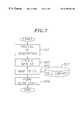
- FIG. 7illustrates a process of creating a digital electronic circuit using a one-pass scan synthesis method of the present invention.
- FIG. 8illustrates a block diagram of another embodiment of a scan flip-flop of the present invention.
- FIG. 2illustrates a scan flip-flop of the present invention.
- a scan flip-flophas a multiplexer 51 with D IN 37 , S IN 43 and test mode signal ⁇ overscore (N) ⁇ /T 23 inputs.
- the multiplexerhas a single output.
- the output of the multiplexeris set to D IN when the test mode signal is set to ⁇ overscore (TEST) ⁇ , and the output of the multiplexer is set to S IN when the test mode signal is set to ⁇ overscore (TEST) ⁇ .
- the output of the multiplexeris connected to an input of a transfer gate 53 .
- the transfer gate 53also receives a clock signal (CLK) the complement of the clock signal ( ⁇ overscore (CLK) ⁇ ).
- the complement of the clock signalis generally internally generated by elements included in a cell containing the scan flip-flop, and methods for doing so are well known in the art.
- the cellneed not, however, contain such elements, with the complement of the clock signal instead formed outside the cell containing the scan flip-flop.
- On a rising edge of the clock signalthe input to the transfer gate is passed to an output 54 of the transfer gate.
- the output of the transfer gateis connected to an input of a latch 55 .
- the latch 55is comprised of a feed forward inverter 55 A and a parallel weak feedback inverter 55 B.
- the output of the latch 55is connected to a second transfer gate 57 , which also has as inputs a clock CLK signal and the complement of the clock signal.
- the output of the second transfer gate 57is connected to an input of a second latch 59 comprised of a feed forward inverter 59 A and a weak feedback inverter 59 B. Accordingly, the transfer gate 53 and the latch 55 form a master portion of the flip-flop, and the transfer gate 57 and the latch 59 form a slave portion of the flip-flop.
- An inverter 61is connected to the output of a second latch 59 .
- the output 119 of the inverter 61is the data output Q of the scan flip-flop.
- the inverter 61therefore functions as a data signal driver for the flip-flop.
- FIG. 6Aillustrates a timing diagram showing a race condition during a scan shift using the digital logic circuit of FIG. 1, and specifically using the scan flip-flops 15 D and 15 E.
- the rising edge of a clock signalarrives at scan flip-flop 15 D.
- the rising edge of the clock signalcauses the Q output of the scan flip-flop 15 D to be set to the value of the signal at the S IN input.
- the Q outputis not set to a new value, however, until time t 2A .
- a portion of the time period t 2A -t 1Ais due to signal propagation time within the scan flip-flop 15 D, and a portion of the time period is due to the time required for a signal driver gate of the scan flip-flop 15 D to transition the Q output to the new value.
- the new Q output signalthen propagates along the signal path between the Q output of scan flip-flop 15 D and the S IN input of scan flip-flop 15 E, with the new Q output signal reaching the S IN input of scan flip-flop 15 E at time t 4A .
- Other circuitsmay also include gates along the signal path, which may cause the time period t 4A -t 2A to be greater.
- the clock signaldoes not arrive at scan flip-flop 15 D and scan flip-flop 15 E at the same time due to clock skew. Instead, the clock signal arrives at scan flip-flop 15 E at time t 3A , which is just prior to time t 4A .
- edge triggered flip-flop operationrequires that an input data signal be steady from a time t s , the setup time, prior to the arrival of a clock signal edge until a time t h , the hold time, after the arrival of the clock signal edge. Changes to the input data signal of an edge triggered flip-flop during the t s to the window may result in an unstable or unexpected response by the flip-flop.
- t gdelay due to any gates in the signal path between the source and destination flip-flop
- t codelay due to signal propagation within the source flip-flop
- clock skewtime period between arrival of a latching clock edge to the source flip-flop and application of the latching clock edge to the destination flip-flop.
- race conditions during scan shift operationsmay be avoided by increasing the signal transition time of a flip-flop during a shift operation. This can be accomplished by decreasing the current drive capability of the inverter 61 . Decreasing the current drive capability of the inverter 61 , however, also modifies circuit behavior during non-scan shift operation, and may do so in undesirable ways.
- source flip-flop transition timeis increased by adding a separate scan-out output port to the flip-flop. This is accomplished by connecting an inverter 63 to the output of the inverter 61 .
- the output of the inverter 63provides a scan-out output to the flip-flop.
- the inverter 63presents a substantially known load to the inverter 61 , which the circuit designer may take into account when designing a circuit.
- the inverter 63may be made a weak signal driver by decreasing its current drive capability.
- the current drive capability of the CMOS deviceis generally proportional to ⁇ w/l, where ⁇ is the carrier mobility of the device, w is the channel width of the device, and l is the channel length of the device.
- ⁇is the carrier mobility of the device
- wis the channel width of the device
- lis the channel length of the device.
- both n-type and p-type transistorsgenerally have a w/l ratio of approximately 8-120.
- the w/l ratiois approximately 30% to 70% of the w/l ratio for a normal driver.
- the weak signal driver providing the scan-out outputhas a w/l ratio less than 25, and preferably less than 20. The strength of the signal driver must, of course, be sufficient to drive a signal to the next flip-flop in the scan chain.
- FIG. 8illustrates another embodiment of a scan flip-flop of the present invention which uses a test clock signal.
- the scan flip-flop of FIG. 8has data-in (D IN ) 37 and scan-in (S IN ) 43 inputs.
- the scan flip-flop of FIG. 8also receives a clock (CLK) signal and a test clock (TCLK) signal, with their complements generally internally generated, as with the scan flip-flop of FIG. 2, by elements included in a cell containing the scan flip-flop.
- CLKclock
- TCLKtest clock
- the output of the master data-in latch circuitis provided to a slave data-in transfer gate 93 , the output of which is provided to a slave latch circuit 94 .
- the scan-in inputis provided to a master scan-in transfer gate 95 , the output of which is provided to a master scan-in latch circuit 96 .
- the output of the master scan-in latch circuitis provided to a slave scan-in transfer gate 97 , the output of which is also provided to the slave latch circuit.
- the output of the slave latch circuitis provided to a data-out signal driver 61 and a scan-out signal driver 63 . Accordingly, the scan flip-flop of FIG. 8 behaves in a manner similar to the scan flip-flop of FIG.
- the scan flip-flop of FIG. 8is a two clock signal (normal clock and test clock) scan flip-flop. Additionally, in the scan flip-flop of FIG. 8 the scan-out signal driver is provided a signal from an internal node on the output data path instead of from the data-out signal driver. Providing the scan-out signal driver a signal from the internal node, instead of from the data-out signal driver, however, reduces the total signal path delay in the scan-out signal path.
- FIG. 3illustrates a scan flip-flop substantially similar to the scan flip-flop of FIG. 2 .
- the scan flip-flop of FIG. 3additionally includes a pair of inverters 65 , 67 .
- the inverters 65 , 67are placed in the signal path between the output of the data signal driver 61 and the input of the scan-out signal driver inverter 63 .
- the inverters 65 , 67act as delay elements, delaying the propagation of the signal within the scan flip-flop.
- the inverter 65whose input is coupled to the output of the data output signal driver inverter 61 , presents a substantially known load to the data signal driver inverter 61 .
- the scan flip-flops of FIGS. 2 and 3provide for the decreased possibility of a race condition during scan shift operation while also decoupling the effect of scan stitching and associated wires from impacting normal circuit operation.
- FIG. 5illustrates in block form a multiplexer which may also be used to reduce the possibility of the occurrence of a race condition during a scan shift operation.
- the multiplexerhas D IN 37 , S IN 43 , and test mode ⁇ overscore (N) ⁇ /T 23 inputs.
- the D IN and S IN inputsare connected to inputs of gated inverters 81 and 83 , respectively.
- the complement of the test mode ⁇ overscore (N) ⁇ /T inputis used to gate the gated inverter 81
- the ⁇ overscore (N) ⁇ /T inputis used to gate the gated inverter 83 .
- the purpose of the gated inverters 81 and 83is to pass the D IN signal, albeit inverted, to the output of the multiplexer when the test mode signal ⁇ overscore (N) ⁇ /T is set to ⁇ overscore (TEST) ⁇ , and to pass the S IN signally albeit inverted, to the output of the multiplexer when the test mode signal ⁇ overscore (N) ⁇ /T is set to ⁇ overscore (TEST) ⁇ .
- Alternative methods and circuits for accomplishing such a resultare well known in the art, and a variety of methods and circuits could be so used.
- the propagation of the S IN signal from the input of the multiplexer to the output of the multiplexeris delayed by inverters 85 and 87 placed in the S IN to multiplexer signal path.
- the inverters 85 and 87effectively serve to decrease or make negative the hold time t h of the scan flip-flop. More specifically, the inverters cause the t s -t h window of the scan flip-flop to be based on a point in time prior to receipt of the clock signal by the scan flip-flop.
- FIG. 4illustrates the digital logic circuit of FIG. 1 with the scan flip-flops replaced with the scan flip-flops of either FIG. 2 or FIG. 3 .
- the digital logic circuit of FIG. 2has combinational circuit elements 31 , 33 and scan flip-flops 35 A- 35 G.
- the signal connection within the digital logic circuit of FIG. 2are the same as within the digital logic circuit of FIG. 1, with the exception that the Q data output signals are no longer connected to the S IN input of the next scan flip-flop in the scan chain. Instead, the additional output ports S out of the scan flip-flop 35 A-G are used to provide a signal to the S IN input ports of the next scan flip-flop in the scan chain and thereby stitch together the scan chain.
- FIG. 6BA timing diagram illustrating a scan shift operation for the circuit of FIG. 4 is shown in FIG. 6B.
- a clock signalis applied to scan flip-flop 115 D at time t 1B .
- the data input to scan flip-flop 115 Dpropagates through the scan flip-flop 115 D and the scan flip-flop Q data driver causes the Q output to transition to the new output value corresponding to the data input value.
- the weak scan-out signal driver of the scan flip-flop of FIG.2the delay buffer of the scan flip-flop of FIG.3, or both, the Sut output does not transition to the new output value until time t 3B .
- circuit designersuse cell libraries, often indirectly, to construct circuits, with each cell in the cell library representing a circuit element.
- circuit designersdesign circuit operation by using a high level language description such as a hardware description language (HDL), of which Verilog VHDL is an example.
- HDLhardware description language
- the HDLis generally provided to a compiler which creates a net list containing the specific logic components of the circuit and the connections between the components that comprise the circuit.
- the compilerthen utilizes the net list to map specific cells from a cell library to each of the components.
- the cellsrepresent, or specify, actual circuit elements. Placement of the scan flip-flops of FIGS.
- FIG. 7A method of this process is illustrated in FIG. 7.
- a circuit designerprovides an HDL description to an HDL compiler in Step 301 .
- HDL compilersare well known, and are available from companies such as Synopsys, Inc.
- the HDL compilergenerates a generic or unmapped net list.
- the net listis passed to an optimization and mapping tool, such as Design Compiler by Synopsys, Inc., which maps cells from a cell library 307 to logic components in the net list in Step 305 .
- the scan flip-flopsare stitched together to form a scan chain.
- Steps 303 , the creation of the net list, and Step 305 , the mapping of cells to logic componentsoccur in a seamless process, but are described separately herein for the purposes of clarity. Further, the scan chain may also be formed during the creation of the net list or during the mapping of cells to logic components, or both.
- the present inventionprovides a scan flip-flop and methodology which reduce the occurrence of race conditions during scan shift operations as well as improves the design process.
- this inventionhas been described in certain specific embodiments, many additional modifications and variations, such as the use of a scan flip-flop having separate scan data clock instead of a multiplexer and associated control signal, would be apparent to those skilled in the art. It is therefore to be understood that this invention may be practiced otherwise than is specifically described.
- the present embodiments of the inventionshould be considered in all respects as illustrative and not restricted, the scope of the invention to be indicated by the appended claims rather than the foregoing description.
Landscapes
- Engineering & Computer Science (AREA)
- General Engineering & Computer Science (AREA)
- Physics & Mathematics (AREA)
- General Physics & Mathematics (AREA)
- Tests Of Electronic Circuits (AREA)
- Semiconductor Integrated Circuits (AREA)
Abstract
Description
Claims (27)
Priority Applications (2)
| Application Number | Priority Date | Filing Date | Title |
|---|---|---|---|
| US09/088,754US6389566B1 (en) | 1998-06-02 | 1998-06-02 | Edge-triggered scan flip-flop and one-pass scan synthesis methodology |
| PCT/US1999/011986WO1999063354A1 (en) | 1998-06-02 | 1999-06-01 | Edge-triggered scan flip-flop and one-pass scan synthesis methodology |
Applications Claiming Priority (1)
| Application Number | Priority Date | Filing Date | Title |
|---|---|---|---|
| US09/088,754US6389566B1 (en) | 1998-06-02 | 1998-06-02 | Edge-triggered scan flip-flop and one-pass scan synthesis methodology |
Publications (1)
| Publication Number | Publication Date |
|---|---|
| US6389566B1true US6389566B1 (en) | 2002-05-14 |
Family
ID=22213253
Family Applications (1)
| Application Number | Title | Priority Date | Filing Date |
|---|---|---|---|
| US09/088,754Expired - LifetimeUS6389566B1 (en) | 1998-06-02 | 1998-06-02 | Edge-triggered scan flip-flop and one-pass scan synthesis methodology |
Country Status (2)
| Country | Link |
|---|---|
| US (1) | US6389566B1 (en) |
| WO (1) | WO1999063354A1 (en) |
Cited By (34)
| Publication number | Priority date | Publication date | Assignee | Title |
|---|---|---|---|---|
| US20020184584A1 (en)* | 2001-05-31 | 2002-12-05 | Matsushita Electric Industrial Co., Ltd. | Scan flip-flop circuit, logic macro, scan test circuit, and method for laying out the same |
| US20030016042A1 (en)* | 2001-07-19 | 2003-01-23 | Parker Kenneth P. | Methods and apparatus for minimizing current surges during integrated circuit testing |
| US6625784B1 (en)* | 1999-08-23 | 2003-09-23 | Matsushita Electric Industrial Co., Ltd. | Semiconductor integrated circuit device, method of testing the same, database for design of the same and method of designing the same |
| US6687890B2 (en)* | 2001-04-13 | 2004-02-03 | Fujitsu Limited | Method for layout design and timing adjustment of logically designed integrated circuit |
| US6717437B2 (en)* | 2001-03-21 | 2004-04-06 | Infineon Technologies Ag | Semiconductor module |
| US20040150421A1 (en)* | 2003-01-08 | 2004-08-05 | Nec Electronics Corporation | Terminating resistor device and a method for testing a terminating resistor circuit |
| US20050046450A1 (en)* | 2003-08-25 | 2005-03-03 | Song Ho Uk | Pre-driver circuit and data output circuit using the same |
| US20050216807A1 (en)* | 2002-03-01 | 2005-09-29 | Barbera George E | System and method for testing a circuit |
| US20050251763A1 (en)* | 2004-05-04 | 2005-11-10 | Hugo Cheung | Methods and apparatus for scan insertion |
| US20060085709A1 (en)* | 2004-10-02 | 2006-04-20 | Kim Chung-Hee | Flip flop circuit & same with scan function |
| WO2006100533A1 (en) | 2005-03-23 | 2006-09-28 | Freescale Semiconductor, Inc. | Method for race prevention and a device having race prevention capabilities |
| US20060255870A1 (en)* | 2005-04-22 | 2006-11-16 | Stmicroelectronics Sa | Multivibrator protected against current or voltage spikes |
| US20070001733A1 (en)* | 2005-06-30 | 2007-01-04 | Texas Instruments Incorporated | Digital storage element architecture comprising integrated 2-to-1 multiplexer functionality |
| US20070001730A1 (en)* | 2005-06-30 | 2007-01-04 | Texas Instruments Incorporated | Digital storage element architecture comprising integrated 4-to-1 multiplexer functionality |
| US20070001732A1 (en)* | 2005-06-30 | 2007-01-04 | Texas Instruments Incorporated | Digital storage element with dual behavior |
| US20070001729A1 (en)* | 2005-06-30 | 2007-01-04 | Texas Instruments Incorporated | Digital storage element architecture comprising dual scan clocks and preset functionality |
| US20070001731A1 (en)* | 2005-06-30 | 2007-01-04 | Texas Instruments Incorporated | Digital storage element architecture comprising integrated multiplexer and reset functionality |
| US7233184B1 (en)* | 2005-06-22 | 2007-06-19 | Xilinx, Inc. | Method and apparatus for a configurable latch |
| US20080091995A1 (en)* | 2006-09-25 | 2008-04-17 | Dong Hyun Baik | Progressive random access scan circuitry |
| US20080115025A1 (en)* | 2006-10-18 | 2008-05-15 | Arm Limited | Circuit and method operable in functional and diagnostic modes |
| US20080284480A1 (en)* | 2007-05-15 | 2008-11-20 | Ati Technologies Ulc | Scan flip-flop with internal latency for scan input |
| US7596732B2 (en) | 2005-06-30 | 2009-09-29 | Texas Instruments Incorporated | Digital storage element architecture comprising dual scan clocks and gated scan output |
| US20100162058A1 (en)* | 2008-12-22 | 2010-06-24 | Lsi Corporation | Sequential element low power scan implementation |
| US7843218B1 (en) | 2009-10-28 | 2010-11-30 | Freescale Semiconductor, Inc. | Data latch with structural hold |
| US20110072326A1 (en)* | 2009-09-23 | 2011-03-24 | Sun Microsystems, Inc. | Sram macro test flop |
| US7962805B1 (en) | 2008-02-06 | 2011-06-14 | Freescale Semiconductor, Inc. | System and method for preventing a race condition |
| US7996805B2 (en) | 2008-01-08 | 2011-08-09 | National Semiconductor Corporation | Method of stitching scan flipflops together to form a scan chain with a reduced wire length |
| US9305590B2 (en) | 2007-10-16 | 2016-04-05 | Seagate Technology Llc | Prevent data storage device circuitry swap |
| US9310435B2 (en) | 2013-10-21 | 2016-04-12 | Global Unichip Corporation | Scan flip-flop and associated method |
| US9679602B2 (en) | 2006-06-14 | 2017-06-13 | Seagate Technology Llc | Disc drive circuitry swap |
| US10417363B1 (en)* | 2016-12-27 | 2019-09-17 | Cadence Design Systems, Inc. | Power and scan resource reduction in integrated circuit designs having shift registers |
| US10509072B2 (en)* | 2017-03-03 | 2019-12-17 | Mentor Graphics Corporation | Test application time reduction using capture-per-cycle test points |
| US11152922B2 (en) | 2019-06-13 | 2021-10-19 | Samsung Electronics Co., Ltd. | Semiconductor device |
| US20250258221A1 (en)* | 2024-02-12 | 2025-08-14 | International Business Machines Corporation | Co-debug of processing conditions of logic devices |
Citations (24)
| Publication number | Priority date | Publication date | Assignee | Title |
|---|---|---|---|---|
| US4495629A (en) | 1983-01-25 | 1985-01-22 | Storage Technology Partners | CMOS scannable latch |
| US4588944A (en) | 1983-06-13 | 1986-05-13 | Sperry Corporation | Fully scan-set testable embedded edge-triggered dual D and J-K flip-flops through testing as inverter strings |
| US4937770A (en)* | 1986-02-07 | 1990-06-26 | Teradyne, Inc. | Simulation system |
| US5329471A (en)* | 1987-06-02 | 1994-07-12 | Texas Instruments Incorporated | Emulation devices, systems and methods utilizing state machines |
| US5452239A (en)* | 1993-01-29 | 1995-09-19 | Quickturn Design Systems, Inc. | Method of removing gated clocks from the clock nets of a netlist for timing sensitive implementation of the netlist in a hardware emulation system |
| EP0702242A2 (en) | 1994-09-01 | 1996-03-20 | STMicroelectronics Limited | Single clock scan latch |
| EP0709688A1 (en) | 1994-10-31 | 1996-05-01 | STMicroelectronics Limited | A scan latch and test method therefore |
| US5625567A (en) | 1993-11-12 | 1997-04-29 | Viewlogic Systems, Inc. | Electronic circuit design system and method with programmable addition and manipulation of logic elements surrounding terminals |
| US5629838A (en)* | 1993-06-24 | 1997-05-13 | Polychip, Inc. | Apparatus for non-conductively interconnecting integrated circuits using half capacitors |
| US5633606A (en)* | 1995-05-25 | 1997-05-27 | National Semiconductor Corporation | Scan flip-flop that holds state during shifting |
| US5636228A (en) | 1996-01-16 | 1997-06-03 | Motorola, Inc. | Scan register with decoupled scan routing |
| US5654658A (en) | 1994-09-22 | 1997-08-05 | Fujitsu Limited | Flip-flop circuit and electronic device including the flip-flop circuit |
| US5684808A (en) | 1995-09-19 | 1997-11-04 | Unisys Corporation | System and method for satisfying mutually exclusive gating requirements in automatic test pattern generation systems |
| US5703789A (en) | 1995-12-29 | 1997-12-30 | Synopsys, Inc. | Test ready compiler for design for test synthesis |
| US5706296A (en)* | 1995-02-28 | 1998-01-06 | Texas Instruments Incorporated | Bi-directional scan design with memory and latching circuitry |
| US5715171A (en) | 1995-05-24 | 1998-02-03 | Mitsubishi Denki Kabushiki Kaisha | Logical synthesizing device, logical synthesizing method, and semiconductor integrated circuit |
| US5790771A (en)* | 1996-05-01 | 1998-08-04 | Hewlett-Packard Company | Apparatus and method for configuring a reconfigurable electronic system having defective resources |
| US5805197A (en)* | 1995-12-28 | 1998-09-08 | Eastman Kodak Company | Driver IC with automatic token direction self-sensing circuitry |
| US5847561A (en)* | 1994-12-16 | 1998-12-08 | Texas Instruments Incorporated | Low overhead input and output boundary scan cells |
| US5859860A (en)* | 1994-12-16 | 1999-01-12 | Texas Instruments Incorporated | Low overhead input and output boundary scan cells |
| US5859657A (en)* | 1995-12-28 | 1999-01-12 | Eastman Kodak Company | Led printhead and driver chip for use therewith having boundary scan test architecture |
| US5872908A (en)* | 1995-05-31 | 1999-02-16 | Texas Instruments Incorporated | IC with isolated analog signal path for testing |
| US5898703A (en)* | 1997-06-05 | 1999-04-27 | Mitsubishi Denki Kabushiki Kaisha | Device and method for testing integrated circuit including bi-directional test pin for receiving control data and outputting observation data |
| US6055659A (en)* | 1999-02-26 | 2000-04-25 | Texas Instruments Incorporated | Boundary scan with latching output buffer and weak input buffer |
- 1998
- 1998-06-02USUS09/088,754patent/US6389566B1/ennot_activeExpired - Lifetime
- 1999
- 1999-06-01WOPCT/US1999/011986patent/WO1999063354A1/enactiveApplication Filing
Patent Citations (24)
| Publication number | Priority date | Publication date | Assignee | Title |
|---|---|---|---|---|
| US4495629A (en) | 1983-01-25 | 1985-01-22 | Storage Technology Partners | CMOS scannable latch |
| US4588944A (en) | 1983-06-13 | 1986-05-13 | Sperry Corporation | Fully scan-set testable embedded edge-triggered dual D and J-K flip-flops through testing as inverter strings |
| US4937770A (en)* | 1986-02-07 | 1990-06-26 | Teradyne, Inc. | Simulation system |
| US5329471A (en)* | 1987-06-02 | 1994-07-12 | Texas Instruments Incorporated | Emulation devices, systems and methods utilizing state machines |
| US5452239A (en)* | 1993-01-29 | 1995-09-19 | Quickturn Design Systems, Inc. | Method of removing gated clocks from the clock nets of a netlist for timing sensitive implementation of the netlist in a hardware emulation system |
| US5629838A (en)* | 1993-06-24 | 1997-05-13 | Polychip, Inc. | Apparatus for non-conductively interconnecting integrated circuits using half capacitors |
| US5625567A (en) | 1993-11-12 | 1997-04-29 | Viewlogic Systems, Inc. | Electronic circuit design system and method with programmable addition and manipulation of logic elements surrounding terminals |
| EP0702242A2 (en) | 1994-09-01 | 1996-03-20 | STMicroelectronics Limited | Single clock scan latch |
| US5654658A (en) | 1994-09-22 | 1997-08-05 | Fujitsu Limited | Flip-flop circuit and electronic device including the flip-flop circuit |
| EP0709688A1 (en) | 1994-10-31 | 1996-05-01 | STMicroelectronics Limited | A scan latch and test method therefore |
| US5847561A (en)* | 1994-12-16 | 1998-12-08 | Texas Instruments Incorporated | Low overhead input and output boundary scan cells |
| US5859860A (en)* | 1994-12-16 | 1999-01-12 | Texas Instruments Incorporated | Low overhead input and output boundary scan cells |
| US5706296A (en)* | 1995-02-28 | 1998-01-06 | Texas Instruments Incorporated | Bi-directional scan design with memory and latching circuitry |
| US5715171A (en) | 1995-05-24 | 1998-02-03 | Mitsubishi Denki Kabushiki Kaisha | Logical synthesizing device, logical synthesizing method, and semiconductor integrated circuit |
| US5633606A (en)* | 1995-05-25 | 1997-05-27 | National Semiconductor Corporation | Scan flip-flop that holds state during shifting |
| US5872908A (en)* | 1995-05-31 | 1999-02-16 | Texas Instruments Incorporated | IC with isolated analog signal path for testing |
| US5684808A (en) | 1995-09-19 | 1997-11-04 | Unisys Corporation | System and method for satisfying mutually exclusive gating requirements in automatic test pattern generation systems |
| US5805197A (en)* | 1995-12-28 | 1998-09-08 | Eastman Kodak Company | Driver IC with automatic token direction self-sensing circuitry |
| US5859657A (en)* | 1995-12-28 | 1999-01-12 | Eastman Kodak Company | Led printhead and driver chip for use therewith having boundary scan test architecture |
| US5703789A (en) | 1995-12-29 | 1997-12-30 | Synopsys, Inc. | Test ready compiler for design for test synthesis |
| US5636228A (en) | 1996-01-16 | 1997-06-03 | Motorola, Inc. | Scan register with decoupled scan routing |
| US5790771A (en)* | 1996-05-01 | 1998-08-04 | Hewlett-Packard Company | Apparatus and method for configuring a reconfigurable electronic system having defective resources |
| US5898703A (en)* | 1997-06-05 | 1999-04-27 | Mitsubishi Denki Kabushiki Kaisha | Device and method for testing integrated circuit including bi-directional test pin for receiving control data and outputting observation data |
| US6055659A (en)* | 1999-02-26 | 2000-04-25 | Texas Instruments Incorporated | Boundary scan with latching output buffer and weak input buffer |
Non-Patent Citations (15)
| Title |
|---|
| Angelotti, et al., Feb. 10, 1998, U.S. Pat. No. 5,717,701 (Abstract only). |
| Boyle, et al., Jan. 5, 1988, U.S. Pat. No. 4,718,065 (Abstract only). |
| Gaudet, et al., May 27, 1997, U.S. Pat. No. 5,633,606 (Abstract only). |
| Gillis, et al., Feb. 17, 1998, U.S. Pat. No. 5,719,879 (Abstract only). |
| Greenstein, et al., Dec. 2, 1997, U.S. Pat. No. 5,694,403 (Abstract only). |
| Koo, et al., Jan. 31, 1995, U.S. Pat. No. 5,386,423 (Abstract only). |
| Maeno, Mar. 23, 1993, U.S. Pat. No. 5,197,070 (Abstract only). |
| Meltzer, Aug. 6, 1996, U.S. Pat. No. 5,544,173 (Abstract only). |
| Moughanni, et al., Jun. 3, 1997, U.S. Pat. No. 5,636,228 (Abstract only). |
| Nakata, Dec. 24, 1996, U.S. Pat. No. 5,588,008 (Abstract only). |
| Ozaki, Aug. 9, 1994, U.S. Pat. No. 5,337,321 (Abstract only). |
| Read, et al., Sep. 30, 1997, U.S. Pat. No. 5,673,295 (Abstract only). |
| Rosales, Jul. 21, 1992, U.S. Pat. No. 5,132,974 (Abstract only). |
| Sturges, Feb. 13, 1996, U.S. Pat. No. 5,491,666 (Abstract only). |
| Valind, Nov. 4, 1997, U.S. Pat. No. 5,684,808 (Abstract only). |
Cited By (57)
| Publication number | Priority date | Publication date | Assignee | Title |
|---|---|---|---|---|
| US6625784B1 (en)* | 1999-08-23 | 2003-09-23 | Matsushita Electric Industrial Co., Ltd. | Semiconductor integrated circuit device, method of testing the same, database for design of the same and method of designing the same |
| US6717437B2 (en)* | 2001-03-21 | 2004-04-06 | Infineon Technologies Ag | Semiconductor module |
| US6687890B2 (en)* | 2001-04-13 | 2004-02-03 | Fujitsu Limited | Method for layout design and timing adjustment of logically designed integrated circuit |
| US6920594B2 (en)* | 2001-05-31 | 2005-07-19 | Matsushita Electric Industrial Co., Ltd. | Scan flip-flop circuit, logic macro, scan test circuit, and method for laying out the same |
| US20020184584A1 (en)* | 2001-05-31 | 2002-12-05 | Matsushita Electric Industrial Co., Ltd. | Scan flip-flop circuit, logic macro, scan test circuit, and method for laying out the same |
| US20030016042A1 (en)* | 2001-07-19 | 2003-01-23 | Parker Kenneth P. | Methods and apparatus for minimizing current surges during integrated circuit testing |
| US7137052B2 (en)* | 2001-07-19 | 2006-11-14 | Verigy Ipco | Methods and apparatus for minimizing current surges during integrated circuit testing |
| US7836365B2 (en)* | 2002-03-01 | 2010-11-16 | Broadcom Corporation | System and method for testing a circuit |
| US20050216807A1 (en)* | 2002-03-01 | 2005-09-29 | Barbera George E | System and method for testing a circuit |
| US7038485B2 (en)* | 2003-01-08 | 2006-05-02 | Nec Electronics Corporation | Terminating resistor device and a method for testing a terminating resistor circuit |
| US20040150421A1 (en)* | 2003-01-08 | 2004-08-05 | Nec Electronics Corporation | Terminating resistor device and a method for testing a terminating resistor circuit |
| US20050046450A1 (en)* | 2003-08-25 | 2005-03-03 | Song Ho Uk | Pre-driver circuit and data output circuit using the same |
| US7477081B2 (en)* | 2003-08-25 | 2009-01-13 | Hynix Semiconductor Inc. | Pre-driver circuit and data output circuit using the same |
| US20050251763A1 (en)* | 2004-05-04 | 2005-11-10 | Hugo Cheung | Methods and apparatus for scan insertion |
| US7155687B2 (en)* | 2004-05-04 | 2006-12-26 | Texas Instruments Incorporated | Methods and apparatus for scan insertion |
| US7590900B2 (en)* | 2004-10-02 | 2009-09-15 | Samsung Electronics Co., Ltd. | Flip flop circuit & same with scan function |
| US20060085709A1 (en)* | 2004-10-02 | 2006-04-20 | Kim Chung-Hee | Flip flop circuit & same with scan function |
| US7941716B2 (en) | 2005-03-23 | 2011-05-10 | Freescale Semiconductor, Inc. | Method for race prevention and a device having race prevention capabilities |
| US20090249142A1 (en)* | 2005-03-23 | 2009-10-01 | Freescale Semiconductor, Inc. | Method for race prevention and a device having race prevention capabilities |
| WO2006100533A1 (en) | 2005-03-23 | 2006-09-28 | Freescale Semiconductor, Inc. | Method for race prevention and a device having race prevention capabilities |
| US7321506B2 (en)* | 2005-04-22 | 2008-01-22 | Stmicroelectronics Sa | Multivibrator protected against current or voltage spikes |
| US20060255870A1 (en)* | 2005-04-22 | 2006-11-16 | Stmicroelectronics Sa | Multivibrator protected against current or voltage spikes |
| US7233184B1 (en)* | 2005-06-22 | 2007-06-19 | Xilinx, Inc. | Method and apparatus for a configurable latch |
| US20070001729A1 (en)* | 2005-06-30 | 2007-01-04 | Texas Instruments Incorporated | Digital storage element architecture comprising dual scan clocks and preset functionality |
| US20070001731A1 (en)* | 2005-06-30 | 2007-01-04 | Texas Instruments Incorporated | Digital storage element architecture comprising integrated multiplexer and reset functionality |
| US7345518B2 (en)* | 2005-06-30 | 2008-03-18 | Texas Instruments Incorporated | Digital storage element with dual behavior |
| US20070001733A1 (en)* | 2005-06-30 | 2007-01-04 | Texas Instruments Incorporated | Digital storage element architecture comprising integrated 2-to-1 multiplexer functionality |
| US7274233B2 (en)* | 2005-06-30 | 2007-09-25 | Texas Instruments Incorporated | Digital storage element architecture comprising integrated 4-to-1 multiplexer functionality |
| US7375567B2 (en)* | 2005-06-30 | 2008-05-20 | Texas Instruments Incorporated | Digital storage element architecture comprising dual scan clocks and preset functionality |
| US8692592B2 (en) | 2005-06-30 | 2014-04-08 | Texas Instruments Incorporated | Digital storage element architecture comprising integrated 2-to-1 multiplexer functionality |
| US7274234B2 (en)* | 2005-06-30 | 2007-09-25 | Texas Instruments Incorporated | Digital storage element architecture comprising integrated multiplexer and reset functionality |
| US20070001732A1 (en)* | 2005-06-30 | 2007-01-04 | Texas Instruments Incorporated | Digital storage element with dual behavior |
| US7596732B2 (en) | 2005-06-30 | 2009-09-29 | Texas Instruments Incorporated | Digital storage element architecture comprising dual scan clocks and gated scan output |
| US20070001730A1 (en)* | 2005-06-30 | 2007-01-04 | Texas Instruments Incorporated | Digital storage element architecture comprising integrated 4-to-1 multiplexer functionality |
| US9679602B2 (en) | 2006-06-14 | 2017-06-13 | Seagate Technology Llc | Disc drive circuitry swap |
| US7665001B2 (en)* | 2006-09-25 | 2010-02-16 | Wisconsin Alumni Research Foundation | Progressive random access scan circuitry |
| US20080091995A1 (en)* | 2006-09-25 | 2008-04-17 | Dong Hyun Baik | Progressive random access scan circuitry |
| US20080115025A1 (en)* | 2006-10-18 | 2008-05-15 | Arm Limited | Circuit and method operable in functional and diagnostic modes |
| US8352815B2 (en)* | 2006-10-18 | 2013-01-08 | Arm Limited | Circuit and method operable in functional and diagnostic modes |
| US20080284480A1 (en)* | 2007-05-15 | 2008-11-20 | Ati Technologies Ulc | Scan flip-flop with internal latency for scan input |
| US7649395B2 (en)* | 2007-05-15 | 2010-01-19 | Ati Technologies Ulc | Scan flip-flop with internal latency for scan input |
| US9305590B2 (en) | 2007-10-16 | 2016-04-05 | Seagate Technology Llc | Prevent data storage device circuitry swap |
| US7996805B2 (en) | 2008-01-08 | 2011-08-09 | National Semiconductor Corporation | Method of stitching scan flipflops together to form a scan chain with a reduced wire length |
| US7962805B1 (en) | 2008-02-06 | 2011-06-14 | Freescale Semiconductor, Inc. | System and method for preventing a race condition |
| US8209573B2 (en)* | 2008-12-22 | 2012-06-26 | Lsi Corporation | Sequential element low power scan implementation |
| US20100162058A1 (en)* | 2008-12-22 | 2010-06-24 | Lsi Corporation | Sequential element low power scan implementation |
| US8181073B2 (en)* | 2009-09-23 | 2012-05-15 | Oracle America, Inc. | SRAM macro test flop |
| US20110072326A1 (en)* | 2009-09-23 | 2011-03-24 | Sun Microsystems, Inc. | Sram macro test flop |
| US7843218B1 (en) | 2009-10-28 | 2010-11-30 | Freescale Semiconductor, Inc. | Data latch with structural hold |
| US9557380B2 (en) | 2013-10-21 | 2017-01-31 | Global Unichip Corporation | Scan flip-flop and associated method |
| US9310435B2 (en) | 2013-10-21 | 2016-04-12 | Global Unichip Corporation | Scan flip-flop and associated method |
| US10417363B1 (en)* | 2016-12-27 | 2019-09-17 | Cadence Design Systems, Inc. | Power and scan resource reduction in integrated circuit designs having shift registers |
| US10509072B2 (en)* | 2017-03-03 | 2019-12-17 | Mentor Graphics Corporation | Test application time reduction using capture-per-cycle test points |
| US11152922B2 (en) | 2019-06-13 | 2021-10-19 | Samsung Electronics Co., Ltd. | Semiconductor device |
| US11431326B2 (en) | 2019-06-13 | 2022-08-30 | Samsung Electronics Co., Ltd. | Semiconductor device |
| US20250258221A1 (en)* | 2024-02-12 | 2025-08-14 | International Business Machines Corporation | Co-debug of processing conditions of logic devices |
| US12422476B2 (en)* | 2024-02-12 | 2025-09-23 | International Business Machines Corporation | Co-debug of processing conditions of logic devices |
Also Published As
| Publication number | Publication date |
|---|---|
| WO1999063354A1 (en) | 1999-12-09 |
Similar Documents
| Publication | Publication Date | Title |
|---|---|---|
| US6389566B1 (en) | Edge-triggered scan flip-flop and one-pass scan synthesis methodology | |
| US6108805A (en) | Domino scan architecture and domino scan flip-flop for the testing of domino and hybrid CMOS circuits | |
| US5689517A (en) | Apparatus for scannable D-flip-flop which scans test data independent of the system clock | |
| US5592493A (en) | Serial scan chain architecture for a data processing system and method of operation | |
| US8484523B2 (en) | Sequential digital circuitry with test scan | |
| JP2725258B2 (en) | Integrated circuit device | |
| JP3474214B2 (en) | Logic circuit and test facilitating circuit provided with the logic circuit | |
| CN110390968B (en) | Latch circuit for memory applications | |
| US4780874A (en) | Diagnostic apparatus for a data processing system | |
| US20020057108A1 (en) | Semiconductor integrated circuit | |
| US6853212B2 (en) | Gated scan output flip-flop | |
| US6271700B1 (en) | Semiconductor integrated circuit having scan path | |
| US7237164B1 (en) | Area optimized edge-triggered flip-flop for high-speed memory dominated design | |
| US6529033B1 (en) | Area efficient clock inverting circuit for design for testability | |
| US4831623A (en) | Swap scan testing of digital logic | |
| JP3197026B2 (en) | Scannable register with delay test capability | |
| US20110181331A1 (en) | Integrated circuit with leakage reduction in static nets | |
| van Berkel et al. | Adding synchronous and LSSD modes to asynchronous circuits | |
| US6060924A (en) | Semiconductor integrated circuit which contains scan circuits of different types | |
| US7900103B2 (en) | Scan chain architecture for increased diagnostic capability in digital electronic devices | |
| US6810498B2 (en) | RAM functional test facilitation circuit with reduced scale | |
| US6901544B1 (en) | Scan chain testing of integrated circuits with hard-cores | |
| US20040019830A1 (en) | Test apparatus of semiconductor integrated circuit with hold error preventing function | |
| US7240263B2 (en) | Apparatus for performing stuck fault testings within an integrated circuit | |
| JP3469294B2 (en) | Linear feedback shift register and semiconductor integrated circuit device |
Legal Events
| Date | Code | Title | Description |
|---|---|---|---|
| AS | Assignment | Owner name:S3 INCORPORATED, CALIFORNIA Free format text:ASSIGNMENT OF ASSIGNORS INTEREST;ASSIGNORS:WAGNER, KENNETH D.;IYENGAR, SRINIVASAN R.;AMERIAN, MEHRAN;REEL/FRAME:009215/0783 Effective date:19980529 | |
| AS | Assignment | Owner name:SONICBLUE INCORPORATED, CALIFORNIA Free format text:CHANGE OF NAME;ASSIGNOR:S3 INCORPORATED;REEL/FRAME:011837/0642 Effective date:20001109 | |
| STCF | Information on status: patent grant | Free format text:PATENTED CASE | |
| CC | Certificate of correction | ||
| AS | Assignment | Owner name:TREPTON RESEARCH GROUP, CALIFORNIA Free format text:ASSIGNMENT OF ASSIGNORS INTEREST;ASSIGNORS:BINAR GRAPHICS, INC.;DIAMOND MEDIA SYSTEMS, INC.;FRONT PATH, INC.;AND OTHERS;REEL/FRAME:014646/0812 Effective date:20031009 | |
| AS | Assignment | Owner name:TREPTON RESEARCH GROUP, INC., CALIFORNIA Free format text:ASSIGNMENT OF ASSIGNORS INTEREST;ASSIGNOR:SONICBLUE INCORPORATED;REEL/FRAME:014532/0711 Effective date:20031009 | |
| FPAY | Fee payment | Year of fee payment:4 | |
| AS | Assignment | Owner name:ALTERA CORPORATION, CALIFORNIA Free format text:ASSIGNMENT OF ASSIGNORS INTEREST;ASSIGNOR:TREPTON RESEARCH GROUP;REEL/FRAME:019140/0818 Effective date:20070307 | |
| FPAY | Fee payment | Year of fee payment:8 | |
| FPAY | Fee payment | Year of fee payment:12 |