US6389494B1 - System for interfacing a data storage system to a host utilizing a plurality of busses for carrying end-user data and a separate bus for carrying interface state data - Google Patents
System for interfacing a data storage system to a host utilizing a plurality of busses for carrying end-user data and a separate bus for carrying interface state dataDownload PDFInfo
- Publication number
- US6389494B1 US6389494B1US09/223,519US22351998AUS6389494B1US 6389494 B1US6389494 B1US 6389494B1US 22351998 AUS22351998 AUS 22351998AUS 6389494 B1US6389494 B1US 6389494B1
- Authority
- US
- United States
- Prior art keywords
- directors
- busses
- interface state
- user data
- state data
- Prior art date
- Legal status (The legal status is an assumption and is not a legal conclusion. Google has not performed a legal analysis and makes no representation as to the accuracy of the status listed.)
- Expired - Lifetime
Links
Images


Classifications
- G—PHYSICS
- G06—COMPUTING OR CALCULATING; COUNTING
- G06F—ELECTRIC DIGITAL DATA PROCESSING
- G06F13/00—Interconnection of, or transfer of information or other signals between, memories, input/output devices or central processing units
- G06F13/10—Program control for peripheral devices
- G06F13/12—Program control for peripheral devices using hardware independent of the central processor, e.g. channel or peripheral processor
- G—PHYSICS
- G06—COMPUTING OR CALCULATING; COUNTING
- G06F—ELECTRIC DIGITAL DATA PROCESSING
- G06F3/00—Input arrangements for transferring data to be processed into a form capable of being handled by the computer; Output arrangements for transferring data from processing unit to output unit, e.g. interface arrangements
- G06F3/06—Digital input from, or digital output to, record carriers, e.g. RAID, emulated record carriers or networked record carriers
- G06F3/0601—Interfaces specially adapted for storage systems
- G06F3/0602—Interfaces specially adapted for storage systems specifically adapted to achieve a particular effect
- G06F3/061—Improving I/O performance
- G06F3/0613—Improving I/O performance in relation to throughput
- G—PHYSICS
- G06—COMPUTING OR CALCULATING; COUNTING
- G06F—ELECTRIC DIGITAL DATA PROCESSING
- G06F12/00—Accessing, addressing or allocating within memory systems or architectures
- G06F12/02—Addressing or allocation; Relocation
- G06F12/08—Addressing or allocation; Relocation in hierarchically structured memory systems, e.g. virtual memory systems
- G06F12/0802—Addressing of a memory level in which the access to the desired data or data block requires associative addressing means, e.g. caches
- G06F12/0806—Multiuser, multiprocessor or multiprocessing cache systems
- G06F12/0813—Multiuser, multiprocessor or multiprocessing cache systems with a network or matrix configuration
- G—PHYSICS
- G06—COMPUTING OR CALCULATING; COUNTING
- G06F—ELECTRIC DIGITAL DATA PROCESSING
- G06F13/00—Interconnection of, or transfer of information or other signals between, memories, input/output devices or central processing units
- G06F13/10—Program control for peripheral devices
- G06F13/12—Program control for peripheral devices using hardware independent of the central processor, e.g. channel or peripheral processor
- G06F13/122—Program control for peripheral devices using hardware independent of the central processor, e.g. channel or peripheral processor where hardware performs an I/O function other than control of data transfer
- G—PHYSICS
- G06—COMPUTING OR CALCULATING; COUNTING
- G06F—ELECTRIC DIGITAL DATA PROCESSING
- G06F3/00—Input arrangements for transferring data to be processed into a form capable of being handled by the computer; Output arrangements for transferring data from processing unit to output unit, e.g. interface arrangements
- G06F3/06—Digital input from, or digital output to, record carriers, e.g. RAID, emulated record carriers or networked record carriers
- G06F3/0601—Interfaces specially adapted for storage systems
- G06F3/0628—Interfaces specially adapted for storage systems making use of a particular technique
- G06F3/0655—Vertical data movement, i.e. input-output transfer; data movement between one or more hosts and one or more storage devices
- G06F3/0658—Controller construction arrangements
- G—PHYSICS
- G06—COMPUTING OR CALCULATING; COUNTING
- G06F—ELECTRIC DIGITAL DATA PROCESSING
- G06F3/00—Input arrangements for transferring data to be processed into a form capable of being handled by the computer; Output arrangements for transferring data from processing unit to output unit, e.g. interface arrangements
- G06F3/06—Digital input from, or digital output to, record carriers, e.g. RAID, emulated record carriers or networked record carriers
- G06F3/0601—Interfaces specially adapted for storage systems
- G06F3/0668—Interfaces specially adapted for storage systems adopting a particular infrastructure
- G06F3/0671—In-line storage system
- G06F3/0683—Plurality of storage devices
- G06F3/0689—Disk arrays, e.g. RAID, JBOD
Definitions
- This inventionrelates generally to data storage systems, and more particularly to data storage systems having redundancy arrangements to protect against total system failure in the event of a failure in a component or subassembly of the storage system.
- large host computer systemsrequire large capacity data storage systems.
- These large computer systemsgenerally include data processors which perform many operations on data introduced to the computer system through peripherals including the data storage system. The results of these operations are output to peripherals, including the storage system.
- One type of data storage systemis a magnetic disk storage system.
- a bank of disk drives and the computer systemare coupled together through an interface.
- the interfaceincludes CPU, or “front end”, directors (or controllers) and “back end” disk directors (or controllers).
- the interfaceoperates the directors in such a way that they are transparent to the computer. That is, data is stored in, and retrieved from, the bank of disk drives in such a way that the computer system merely thinks it is operating with one large memory.
- One such systemis described in U.S. Pat. No. 5,206,939, entitled “System and Method for Disk Mapping and Data Retrieval”, inventors Moshe Yanai, Natan Vishlitzky, Bruno Alterescu and Daniel Castel, issued Apr. 27, 1993, and assigned to the same assignee as the present invention.
- the interfacemay also include, in addition to the CPU directors and disk directors, addressable cache memories.
- the cache memoryis a semiconductor memory and is provided to rapidly store data from the computer system before storage in the disk drives, and, on the other hand, store data from the disk drives prior to being sent to the computer.
- the cache memorybeing a semiconductor memory, as distinguished from a magnetic memory as in the case of the disk drives, is much faster than the disk drives in reading and writing data.
- the CPU directors, disk directors and cache memoryare interconnected through a backplane printed circuit board. More particularly, disk directors are mounted on disk director printed circuit boards. CPU directors are mounted on CPU director printed circuit boards. And, cache memories are mounted on cache memory printed circuit boards. The disk director, CPU director and cache memory printed circuit boards plug into the backplane printed circuit board. In order to provide data integrity in case of a failure in a director, the backplane printed circuit board has a pair of buses. One set of the disk directors is connected to one bus and another set of the disk directors is connected to the other bus. Likewise, one set the CPU directors is connected to one bus and another set of the CPU directors is connected to the other bus. The cache memories are connected to both buses. Each one of the buses provides data, address and control information.
- the host computerwhen the host computer wishes to store end-user (i.e., host computer) data at an address, the host computer issues a write request to one of the front-end directors to perform a write command.
- One of the front-end directorsreplies to the request and asks the host computer for the data.
- the directordetermines the size of the end-user data and reserves space in the cache memory to store the request.
- the front-end directorthen produces control signals on either one of the busses connected to such front-end director.
- the host computerthen transfers the data to the front-end director.
- the front-end directoradvises the host computer that the transfer is complete.
- the front-end directorlooks up in a Table, not shown, stored in the cache memory to determine which one of the rear-end directors is to handle this request.
- the Tablemaps the host computer address into an address in the bank of disk drives.
- the front-end directorthen puts a notification in a “mail box” (not shown and stored in the cache memory) for the rear-end director which is to handle the request, the amount of the data and the disk address for the data.
- Other rear-end directorspoll the cache memory when they are idle to check their “mail boxes”. If the polled “mail box” indicates a transfer is to be made, the rear-end director processes the request, addresses the disk drive in the bank, reads the data from the cache memory and writes it into the addresses of a disk drive in the bank.
- the interface systemWhen end-user data previously stored in the bank of disk drives is to be read from the disk drive and returned to the host computer, the interface system operates in a reciprocal manner.
- the internal operation of the interface(e.g. “mail-box polling”, event flags, data structures, device tables, queues, etc.) is controlled by interface state data which passes between the directors through the cache memory.
- end-user datais transferred through the interface as a series of multi-word transfers, or bursts.
- Each word transfer in a multi-word transferis here, for example, 64 bits.
- an end-user data transferis made up of, for example, 32 bursts.
- Each interface state wordis a single word having, for example, 64 bits.
- the end-user data and interface state dataare transferred among the directors and the cache memory on the busses.
- Each one of the two bussesmust share its bandwidth with both end-user data and the interface state data. Therefore, the bandwidth of the system may not be totally allocated to end-user data transfer between the host computer and the bank of disk drives.
- a data storage systemwherein end-user data is transferred between a host computer and a bank of disk drives through an interface.
- the interfaceincludes a memory and a plurality of directors interconnected through an interface state data bus and a plurality of end-user data busses. At least one front-end one of the directors is in communication with the host computer and at least one rear-end one of the directors is in communication with the bank of disk drives.
- the interface state data bus sectionis in communication with: both the at least one front-end one and the at least one rear-end one of the directors; and to the memory.
- Each one of the plurality of end-user data buseshas a first end coupled to a corresponding one of the plurality of directors and a second end coupled to the memory.
- the plurality of directorscontrol the end-user data transfer between the host computer and the bank of disk drives through the memory in response to interface state data generated by the directors as such end-user data passes through the end-user data busses.
- the generated interface state datais transferred among the directors through the memory as such end-user data passes through the end-user bus.
- FIG. 1is a block diagram of a memory system according to the PRIOR ART
- FIG. 2is a block diagram of a memory system according to the invention.
- FIG. 3is a block diagram of an exemplary one of a plurality of cache memory printed circuit boards used in the system of FIG. 2;
- FIG. 4is a block diagram of an exemplary one of a plurality of front-end directors used in the system of FIG. 2;
- FIG. 5is a block diagram of an exemplary one of a plurality of rear-end directors used in the system of FIG. 2;
- FIG. 6is a block diagram of an exemplary one of a plurality of ASIC control logics used in the cache memories of FIG. 3;
- FIG. 7is a block diagram of another embodiment of an interface in accordance with the invention.
- FIG. 8is a block diagram of still another embodiment of an interface in accordance with the invention.
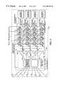
- the computer system 100includes a host computer section 112 (e.g., a main frame or open systems computer section) having a plurality of processors, not shown, for processing end-user data. Portions of the processed end-user data are stored in, and retrieved data from, a bank 116 of disk drives through an interface 118 .
- the interfaceincludes a cache memory section 120 , here made up of two identical cache memory printed circuit boards 120 0 , 120 1 , an exemplary one thereof, here memory board 120 0 being shown in, and to be discussed in detail in connection with, FIG. 3 .
- the memory board 120 0includes an array of DRAMs, here arranged in four memory regions, i.e., memory region A, memory region B. memory region C and memory region D, as shown in FIG. 3 and described in detail in co-pending patent application Ser. No. 09/052,268 now U.S. Pat. No. 5,943,287, entitled “Memory System” filed Mar. 31, 1998, inventor John K. Walton, the entire subject matter thereof being incorporated herein by reference.
- the interface 118also includes a plurality of, here eight directors 122 0 - 122 7 .
- four of the directorsi.e., directors 122 0 - 122 3
- four of the directorsi.e., directors 122 4 - 122 7
- Each one of the front-end directors 122 0 - 123is identical in construction, an exemplary one thereof, here front-end director 122 0 being shown in FIG. 4 .
- a cross-bar switch 123is included to couple each one of a plurality, here four example four, processors, not shown in the host computer 112 , to either port P 0 of cache memory 120 0 via serial bus 126 0,0 , or port P 0 of cache memory 120 1 via serial bus 126 0,1 as indicated.
- each one of the serial bussesis a four wire bus having a differential pair of receive wires and a differential pair of transmit wires.
- each one of the rear-end directors 122 4 - 122 7is identical in construction, an exemplary one thereof, here rear-end director 122 4 being shown in FIG. 5 . It is noted that here a cross-bar switch 123 equivalent to that shown in FIG.
- each one of a plurality, here four example four, rows disk drives, not shown, in bank 116is included to couple each one of a plurality, here four example four, rows disk drives, not shown, in bank 116 , to either port P 4 of cache memory 120 0 via serial bus 126 4,0 or port P 4 of cache memory 120 1 via serial bus 126 4,1 , as indicated.
- the interface 118also includes an interface state data bus section 124 , here made up of four interface state data parallel, here 72 wire, busses, i.e., bus A, bus B, bus C, and bus D, for carrying interface state data through the interface 118 .
- the interface state data bus section 124is coupled to: the front-end directors 122 0 - 122 3 , the rear-end directors 122 4 - 122 7 ; and all to the cache memory printed circuit boards 120 0 , 120 1 .
- each one of the four bussesis a multi-drop bus.
- the interface 118also includes a plurality of, here 16, serial end-user data busses 126 0,0 - 126 7,1 for carrying end-user data, as indicated.
- Each one of the plurality of end-user data busses 126 0,0 - 126 7,1has a first end coupled to a corresponding one of the plurality of directors 122 0 - 122 7 and a second end coupled to the memory section 120 . More particularly, and considering director 122 0 , such director is coupled to memory bard 122 0 through end-user data bus 126 0,0 and to memory board 122 0 through end-user data bus 126 0,1 . Director 122 1 is coupled to memory bard 122 0 through end-user data bus 126 1,0 , and to memory board 122 1 through end-user data bus 126 1,1 ,.
- director 122 7is coupled to memory board 122 0 through end-user data bus 126 7,0 and to memory board 122 1 through end-user data bus 126 7,1 , as shown.
- the plurality of directors 122 0 - 122 7control the end-user data transfer between the host computer 112 and the bank of disk drives 116 through the memory 120 via the end-user data busses 126 0,0 - 126 7,1 in response to interface state data generated by the directors 122 0 - 122 7 .
- the interface state datais generated by the directors 122 0 - 122 7 and is transferred among the directors 122 0 - 122 7 through the memory section 120 via the interface state bus section 124 .
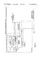
- Such memory section 120 0includes a plurality of, here four random access memory (RAM) regions (i.e. RAM region A, RAM region B, RAM region C and RAM region D, as shown, and a matrix of rows and columns of control logic sections, here Application Specific Integrated circuits (ASICs), i.e, control logic section ASIC A,A . . . control logic section ASIC D,D.
- RAMrandom access memory
- ASICsApplication Specific Integrated circuits
- Each one of the four columns of control logic section ASICsis coupled to a corresponding one of the interface state data busses A, B, C, and D, respectively, as shown.
- a first column of control logic sectionsi.e., ASICs A,A; B,A; C,A and D,A
- a second column of control logic sectionsi.e., ASICs A,B; B,B; C,B and D,B
- a third column of control logic sectionsi.e., ASICs A,C; B,C; C,C and D,C
- a fourth column of control logic sectionsi.e., ASICs A,D; B,D; C,D and D,D
- D busD bus.
- Each one of the rows of the control logic sections ASIC A,A . . . ASIC D,Dis coupled to a corresponding one of the four RAM regions, RAM region A . . . RAM region D, via a DATA/CHIP SELECT, as indicated.
- the first row of ASICs A,A; A,B; A,C; and A,Dis coupled to the DATA/CHIP SELECT BUS of RAM region A.
- the second row of ASICs B,A; B,B; B,C; and B,Dis coupled to the DATA/CHIP SELECT BUS of RAM region B.
- the third row of ASICs C,A; C,B; C,C; and C,Dis coupled to the DATA/CHIP SELECT BUS of RAM region C.
- the fourth row of ASICS D,A; D,B; D,C; and D,Dis coupled to the DATA/CHIP SELECT BUS of RAM region D.
- the control logic sections ASIC A,A . . . ASIC D,D in each of the four rows thereofare interconnected through an arbitration bus, not shown, in a manner described in detail in co-pending patent application entitled “Bus Arbitration System”, Ser. No. 08/996,807, filed Dec. 23, 1997, inventors Christopher S. MacLellan and John K. Walton, assigned to the same assignee as the present invention, the entire subject matter thereof being incorporated in this patent application.
- Each one of the rows of the control logic sections ASIC A,A . . . ASIC D,Dis coupled to a corresponding one of the four RAM regions, RAM region A . . . RAM region D, via an MEMORY ADDRESS/CONTROL BUS, as indicated.
- the first row of ASICs A,A; A,B; A,C; and A,Dis coupled to the MEMORY ADDRESS/CONTROL BUS of RAM region A.
- the second row of ASICs B,A; B,B; B,C; and B,Dis coupled to the MEMORY ADDRESS/MEMORY BUS of RAM region B.
- the third row of ASICs C,A; C,B; C,C; and C,Dis coupled to the MEMORY ADDRESS/CONTROL BUS of RAM region C.
- the fourth row of ASICs D,A; D,B; D,C; and D,Dis coupled to the MEMORY ADDRESS/CONTROL BUS of RAM region D.
- the cache memory 120 0also includes a coupling node 130 adapted to couple any one of the ports P 0 -P 7 to any one of four ports P A , P B , P C , and P D .
- the coupling node 130adapted to couple any one of the ports P 0 -P 7 to any one of the rows of DATA/CHIP SELECT BUSSES, i.e., any one of the ports P 0 -P 7 to any one of the four memory regions, A, B, C or D, selectively in response to control signals produced by the ASICs A,A through D,D on a COUPLING NODE CONTROL BUS of each one of the ASICs A,A through D,D.
- the end-user datais selectively coupled through the coupling node 130 in accordance with routing information fed thereto by the ASICs A,A through D,D in a manner to be described.
- the coupling node 130includes a cross-bar switch section 132 having a plurality of, here two, cross-bar switches 132 a , 132 b .
- the coupling node 130also includes a plurality of, here four, data selectors 134 a through 134 d .
- Each one of the cross-bar switches 132 a , 132 bis a 4 ⁇ 4 cross-bar switch controlled by control signals fed thereto by the ASICs A,A through D,D.
- each one of the crossbar switches 132 a , 132 bas four input/outputs (here coupled to ports P 0 -P 3 , P 4 -P 7 , respectively, as indicated and four output/inputs coupled to a corresponding one of a pair of input/outputs of the four data selectors 134 a through 134 d.
- control logic section ASIC A,Ais identical in construction, an exemplary one thereof, here control logic section ASIC A,A being shown in detail in FIG. 6 to include a control logic 150 having control logic and a buffer memory 152 described in the above-referenced co-pending patent application entitled “TIMING PROTOCOL FOR A DATA STORAGE SYSTEM”, inventor John K. Walton, Ser. No. 08/996,809, filed Dec. 23, 1997, assigned to the same assignee as the present invention, the entire subject matter thereof being incorporated herein by reference.
- the ASIC (A,A)controls transfer of data between the buffer memory 152 and the one of the plurality of buses (i.e., A bus, B bus B, C bus and D bus) coupled to the control logic section ASIC A,A, here bus A.
- the control logic section ASIC A,Ais adapted to produce a control/data bus request for the one of the control/data buses coupled thereto (here RAM region A) and is adapted to effect the transfer in response to a control/data bus grant fed to the control logic section (here ASIC A,A) in accordance with a protocol described in the above-referenced co-pending application entitled “TIMING PROTOCOL FOR A DATA STORAGE SYSTEM”, Ser. No. 08/996,809, inventor John K.
- the control logic section ASIC A,Aalso includes a bus arbitration section 153 described in detail in connection with the above referenced patent application entitled “Bus Arbitration System”, filed Dec. 23, 1997, inventors Christopher S. MacLellan and John K. Walton.
- the arbitration sectionalso arbitrates for memory contention with one addition bus, the one end-user data serial busses coupled to either port P A , P B , P C , or P D by the cross-bar switch section 132 , in addition to busses A, B., C, and, D.
- the control logic 150includes a decoder 157 for decoding the eight chip select signals and one read/write signals on the A bus as described in detail in the above referenced co-pending patent application Ser. No. 09/052,268.
- the decoder 157produces address, control, and clock for the memory region A on the MEMORY ADDRESS/CONTROL BUS, as indicated.
- the routing informationis fed to the ASICs A,A through D,D via the interface state data busses A, B, C, and D.
- the interface state data busses A, B, C, and DFor example, if a burst end-user data is to be transferred from director 122 3 to memory region A of cache memory 120 0 , it is first noted that such director 122 3 is connected to interface state data bus A and therefore the coupling node routing information is for such end-user data transfer is placed by director 122 3 on interface state data bus A.
- the ASIC A,A control logicin response to the coupling node routing information on bus A, presents control information on the COUPLING NODE CONTROL BUS coupled thereto to couple port P 3 of the cache memory 120 0 (which is connected to director 122 3 via end-user bus 126 3,0 ) through cross-bar switch 132 a and selector 134 a to port P A .
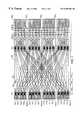
- the interface 118 ′includes 16 directors 122 ′ 0 - 122 ′ 15 and four cache memory printed circuit boards 120 ′ 0 - 120 ′ 3 interconnected through parallel, multi-drop busses A, B, C and D for carrying interface state data and sixty-four sets of serial, point-to-point busses 126 ′ 0,0 - 126 ′ 0,3 through 126 ′ 15,0 - 126 ′ 15,3 for carrying end-user data, as shown.
- each one of the directors 122 ′ 0 - 122 ′ 15includes four cross-bar switches 132 ′, each one being a 4 ⁇ 4 cross-bar switch.
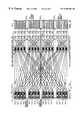
- interface 118 ′′includes 16 directors 122 ′′ 0 - 122 ′′ 15 and four cache memory printed circuit boards 120 ′′ 0 - 120 ′′ 3 interconnected through four parallel, multi-drop busses TH, TL, BH, and BL, such busses being arranged as shown and as described in co-pending patent application entitled “Data Storage System”, inventors Daniel Castel, et al., assigned to the same assignee as the present invention, and filed on the same day as this patent application, the entire subject matter thereof being incorporated herein by reference.
- the cache memoryis arranged to two set; one set having low address and one set having high addresses.
- cache memory printed circuit boards 120 ′′ 0 and 120 ′′ 1are included in the high address memory set and cache memory printed circuit boards 120 ′′ 2 and 120 ′′ 3 are included in the low address memory set.
- the parallel, multi-drop busses THi.e., top high
- TLi.e., top low
- BHbottom high
- BLbottom low B
Landscapes
- Engineering & Computer Science (AREA)
- Theoretical Computer Science (AREA)
- Physics & Mathematics (AREA)
- General Engineering & Computer Science (AREA)
- General Physics & Mathematics (AREA)
- Human Computer Interaction (AREA)
- Mathematical Physics (AREA)
- Memory System Of A Hierarchy Structure (AREA)
- Information Retrieval, Db Structures And Fs Structures Therefor (AREA)
- Bus Control (AREA)
Abstract
Description
Claims (37)
Priority Applications (9)
| Application Number | Priority Date | Filing Date | Title |
|---|---|---|---|
| US09/223,519US6389494B1 (en) | 1998-12-30 | 1998-12-30 | System for interfacing a data storage system to a host utilizing a plurality of busses for carrying end-user data and a separate bus for carrying interface state data |
| JP2000591519AJP4315600B2 (en) | 1998-12-30 | 1999-12-29 | Data storage system |
| DE69919137TDE69919137T2 (en) | 1998-12-30 | 1999-12-29 | DATA STORAGE SYSTEM |
| EP99967760AEP1058889B1 (en) | 1998-12-30 | 1999-12-29 | Data storage system |
| KR1020007009605AKR100585414B1 (en) | 1998-12-30 | 1999-12-29 | Data storage systems |
| PCT/US1999/031213WO2000039691A1 (en) | 1998-12-30 | 1999-12-29 | Data storage system |
| US10/054,241US6988152B2 (en) | 1998-12-30 | 2002-01-22 | Data storage system |
| US10/120,957US6957285B2 (en) | 1998-12-30 | 2002-04-11 | Data storage system |
| JP2006091584AJP2006190338A (en) | 1998-12-30 | 2006-03-29 | Data storage system |
Applications Claiming Priority (1)
| Application Number | Priority Date | Filing Date | Title |
|---|---|---|---|
| US09/223,519US6389494B1 (en) | 1998-12-30 | 1998-12-30 | System for interfacing a data storage system to a host utilizing a plurality of busses for carrying end-user data and a separate bus for carrying interface state data |
Related Child Applications (2)
| Application Number | Title | Priority Date | Filing Date |
|---|---|---|---|
| US10/054,241DivisionUS6988152B2 (en) | 1998-12-30 | 2002-01-22 | Data storage system |
| US10/120,957DivisionUS6957285B2 (en) | 1998-12-30 | 2002-04-11 | Data storage system |
Publications (1)
| Publication Number | Publication Date |
|---|---|
| US6389494B1true US6389494B1 (en) | 2002-05-14 |
Family
ID=22836859
Family Applications (3)
| Application Number | Title | Priority Date | Filing Date |
|---|---|---|---|
| US09/223,519Expired - LifetimeUS6389494B1 (en) | 1998-12-30 | 1998-12-30 | System for interfacing a data storage system to a host utilizing a plurality of busses for carrying end-user data and a separate bus for carrying interface state data |
| US10/054,241Expired - LifetimeUS6988152B2 (en) | 1998-12-30 | 2002-01-22 | Data storage system |
| US10/120,957Expired - LifetimeUS6957285B2 (en) | 1998-12-30 | 2002-04-11 | Data storage system |
Family Applications After (2)
| Application Number | Title | Priority Date | Filing Date |
|---|---|---|---|
| US10/054,241Expired - LifetimeUS6988152B2 (en) | 1998-12-30 | 2002-01-22 | Data storage system |
| US10/120,957Expired - LifetimeUS6957285B2 (en) | 1998-12-30 | 2002-04-11 | Data storage system |
Country Status (6)
| Country | Link |
|---|---|
| US (3) | US6389494B1 (en) |
| EP (1) | EP1058889B1 (en) |
| JP (2) | JP4315600B2 (en) |
| KR (1) | KR100585414B1 (en) |
| DE (1) | DE69919137T2 (en) |
| WO (1) | WO2000039691A1 (en) |
Cited By (46)
| Publication number | Priority date | Publication date | Assignee | Title |
|---|---|---|---|---|
| US20020078292A1 (en)* | 2000-12-19 | 2002-06-20 | Chilton Kendell A. | Methods and apparatus for transferring a data element within a data storage system |
| US6516370B1 (en)* | 1999-12-29 | 2003-02-04 | Emc Corporation | Data storage system |
| US6523077B1 (en)* | 1999-01-14 | 2003-02-18 | Nec Corporation | Data processing apparatus and data processing method accessing a plurality of memories in parallel |
| US6560683B1 (en) | 1999-12-29 | 2003-05-06 | Emc Corporation | Fibre channel data storage system having improved rear-end I/O adapted hub |
| US6567890B1 (en) | 1999-06-30 | 2003-05-20 | Emc Corporation | Fibre channel port by-pass selector section for dual ported disk drives |
| US6571355B1 (en) | 1999-12-29 | 2003-05-27 | Emc Corporation | Fibre channel data storage system fail-over mechanism |
| US6574687B1 (en)* | 1999-12-29 | 2003-06-03 | Emc Corporation | Fibre channel data storage system |
| US6581136B1 (en) | 1999-06-30 | 2003-06-17 | Emc Corporation | Fibre channel data storage system having expansion/contraction |
| US6584513B1 (en) | 2000-03-31 | 2003-06-24 | Emc Corporation | Direct memory access (DMA) transmitter |
| US20030135682A1 (en)* | 2002-01-02 | 2003-07-17 | Fanning Blaise B. | Point-to-point busing and arrangement |
| US6604155B1 (en)* | 1999-11-09 | 2003-08-05 | Sun Microsystems, Inc. | Storage architecture employing a transfer node to achieve scalable performance |
| US6611879B1 (en)* | 2000-04-28 | 2003-08-26 | Emc Corporation | Data storage system having separate data transfer section and message network with trace buffer |
| US6615315B1 (en) | 1999-12-29 | 2003-09-02 | Emc Corporation | Fibre channel data storage system having improved fro-end I/O adapted hub |
| US6629216B1 (en) | 1999-06-30 | 2003-09-30 | Emc Corporation | Fibre channel by-pass |
| US6636934B1 (en) | 1999-06-30 | 2003-10-21 | Emc Corporation | Fiber channel port by-pass selector section for dual ported disk drives |
| US6636933B1 (en)* | 2000-12-21 | 2003-10-21 | Emc Corporation | Data storage system having crossbar switch with multi-staged routing |
| US6651130B1 (en)* | 2000-04-28 | 2003-11-18 | Emc Corporation | Data storage system having separate data transfer section and message network with bus arbitration |
| US20030229757A1 (en)* | 2002-05-24 | 2003-12-11 | Hitachi, Ltd. | Disk control apparatus |
| US20040073750A1 (en)* | 1998-04-27 | 2004-04-15 | Hitachi, Ltd. | Multi-processor type storage control apparatus for performing access control through selector |
| US6757753B1 (en) | 2001-06-06 | 2004-06-29 | Lsi Logic Corporation | Uniform routing of storage access requests through redundant array controllers |
| US6779071B1 (en) | 2000-04-28 | 2004-08-17 | Emc Corporation | Data storage system having separate data transfer section and message network with status register |
| US20040193973A1 (en)* | 2003-03-31 | 2004-09-30 | Ofer Porat | Data storage system |
| US6820171B1 (en)* | 2000-06-30 | 2004-11-16 | Lsi Logic Corporation | Methods and structures for an extensible RAID storage architecture |
| US20040250181A1 (en)* | 2003-06-05 | 2004-12-09 | Intel Corporation | Memory channel with bit lane fail-over |
| US20050071556A1 (en)* | 2003-09-30 | 2005-03-31 | Walton John K. | Data storage system having shared resource |
| US6914784B1 (en) | 2002-06-26 | 2005-07-05 | Emc Corporation | Data storage system cabinet |
| US6944702B1 (en)* | 2002-06-26 | 2005-09-13 | Emc Corporation | Data storage system |
| US6957285B2 (en)* | 1998-12-30 | 2005-10-18 | Emc Corporation | Data storage system |
| US20050254558A1 (en)* | 2004-04-13 | 2005-11-17 | Stephen Charles Dutka | Methods and structures for rapid code acquisition in spread spectrum communications |
| US6993621B1 (en)* | 2000-03-31 | 2006-01-31 | Emc Corporation | Data storage system having separate data transfer section and message network with plural directors on a common printed circuit board and redundant switching networks |
| US7003601B1 (en) | 2000-03-31 | 2006-02-21 | Emc Corporation | Data storage system having separate data transfer section and message network with plural directions on a common printed circuit board |
| US7007194B1 (en) | 2000-06-29 | 2006-02-28 | Emc Corporation | Data storage system having point-to-point configuration |
| US7010575B1 (en) | 2000-03-31 | 2006-03-07 | Emc Corporation | Data storage system having separate data transfer section and message network having bus arbitration |
| US20060134936A1 (en)* | 2004-12-20 | 2006-06-22 | Douglas Sullivan | Multi-function expansion slots for a storage system |
| US7073020B1 (en)* | 1999-01-04 | 2006-07-04 | Emc Corporation | Method for message transfer in computer storage system |
| US7072989B1 (en) | 2002-09-27 | 2006-07-04 | Cypress Semiconductor, Inc. | USB peripheral device storing an indication of an operating power mode when a host went into hibernate and restarting at the power mode accordingly |
| US7117275B1 (en) | 1999-01-04 | 2006-10-03 | Emc Corporation | Data storage system having separate data transfer section and message network |
| US7194638B1 (en) | 2002-09-27 | 2007-03-20 | Cypress Semiconductor Corporation | Device and method for managing power consumed by a USB device |
| US7293118B1 (en) | 2002-09-27 | 2007-11-06 | Cypress Semiconductor Corporation | Apparatus and method for dynamically providing hub or host operations |
| US20080074998A1 (en)* | 2003-01-09 | 2008-03-27 | Becker Wiren D | Self-healing chip-to-chip interface |
| US7395366B1 (en) | 2002-09-27 | 2008-07-01 | Cypress Semiconductor Corp. | System, method, and apparatus for connecting USB peripherals at extended distances from a host computer |
| US7432749B1 (en) | 2004-06-23 | 2008-10-07 | Cypress Semiconductor Corp. | Circuit and method for improving frequency range in a phase locked loop |
| US7447922B1 (en) | 2004-06-23 | 2008-11-04 | Cypress Semiconductor Corp. | Supplying power from peripheral to host via USB |
| US7653123B1 (en) | 2004-09-24 | 2010-01-26 | Cypress Semiconductor Corporation | Dynamic data rate using multiplicative PN-codes |
| US7689724B1 (en) | 2002-08-16 | 2010-03-30 | Cypress Semiconductor Corporation | Apparatus, system and method for sharing data from a device between multiple computers |
| US8135880B2 (en) | 2006-03-31 | 2012-03-13 | Cypress Semiconductor Corporation | USB mass storage locking |
Families Citing this family (11)
| Publication number | Priority date | Publication date | Assignee | Title |
|---|---|---|---|---|
| US6836818B1 (en)* | 1999-09-29 | 2004-12-28 | Emc Corporation | Central processing unit |
| US6543029B1 (en) | 1999-09-29 | 2003-04-01 | Emc Corporation | Error corrector |
| US6915394B1 (en) | 1999-09-29 | 2005-07-05 | Emc Corporation | Microprocessor interface |
| US6735655B1 (en) | 1999-09-29 | 2004-05-11 | Emc Corporation | Interrupt request controller |
| US6519739B1 (en) | 1999-09-29 | 2003-02-11 | Emc Corporation | Fault detector |
| US6581137B1 (en) | 1999-09-29 | 2003-06-17 | Emc Corporation | Data storage system |
| JP3578075B2 (en) | 2000-10-13 | 2004-10-20 | 日本電気株式会社 | Disk array control device and disk array control method |
| US6959310B2 (en)* | 2002-02-15 | 2005-10-25 | International Business Machines Corporation | Generating data set of the first file system by determining a set of changes between data stored in first snapshot of the first file system, and data stored in second snapshot of the first file system |
| JP4220724B2 (en)* | 2002-05-21 | 2009-02-04 | 株式会社日立製作所 | Storage device |
| US7712004B1 (en) | 2003-09-30 | 2010-05-04 | Emc Corporation | Method of and system for error checking in a data storage system |
| US9361973B2 (en)* | 2013-10-28 | 2016-06-07 | Cypress Semiconductor Corporation | Multi-channel, multi-bank memory with wide data input/output |
Citations (14)
| Publication number | Priority date | Publication date | Assignee | Title |
|---|---|---|---|---|
| US4780808A (en)* | 1981-11-27 | 1988-10-25 | Storage Technology Corporation | Control of cache buffer for memory subsystem |
| EP0510821A1 (en) | 1991-04-22 | 1992-10-28 | International Business Machines Corporation | Multiprocessor cache system |
| US5206939A (en) | 1990-09-24 | 1993-04-27 | Emc Corporation | System and method for disk mapping and data retrieval |
| US5586264A (en)* | 1994-09-08 | 1996-12-17 | Ibm Corporation | Video optimized media streamer with cache management |
| US5603058A (en)* | 1994-09-08 | 1997-02-11 | International Business Machines Corporation | Video optimized media streamer having communication nodes received digital data from storage node and transmitted said data to adapters for generating isochronous digital data streams |
| EP0795812A1 (en) | 1994-11-11 | 1997-09-17 | Hitachi, Ltd. | Disk array controller and disk array device |
| US5742789A (en)* | 1995-12-28 | 1998-04-21 | Emc Corporation | Dynamically adaptive data retrieval for a disk drive storage system |
| US5787265A (en) | 1995-09-28 | 1998-07-28 | Emc Corporation | Bus arbitration system having a pair of logic networks to control data transfer between a memory and a pair of buses |
| US5799209A (en)* | 1995-12-29 | 1998-08-25 | Chatter; Mukesh | Multi-port internally cached DRAM system utilizing independent serial interfaces and buffers arbitratively connected under a dynamic configuration |
| US5805821A (en)* | 1994-09-08 | 1998-09-08 | International Business Machines Corporation | Video optimized media streamer user interface employing non-blocking switching to achieve isochronous data transfers |
| US5819054A (en) | 1993-06-30 | 1998-10-06 | Hitachi, Ltd. | Storage system realizing scalability and fault tolerance |
| US5819104A (en)* | 1996-06-24 | 1998-10-06 | Emc Corporation | Disk array memory system having bus repeater at disk backplane |
| US5948062A (en)* | 1995-10-27 | 1999-09-07 | Emc Corporation | Network file server using a cached disk array storing a network file directory including file locking information and data mover computers each having file system software for shared read-write file access |
| US6055603A (en)* | 1997-09-18 | 2000-04-25 | Emc Corporation | Method and apparatus for performing pre-request operations in a cached disk array storage system |
Family Cites Families (71)
| Publication number | Priority date | Publication date | Assignee | Title |
|---|---|---|---|---|
| US4484262A (en) | 1979-01-09 | 1984-11-20 | Sullivan Herbert W | Shared memory computer method and apparatus |
| US4438494A (en) | 1981-08-25 | 1984-03-20 | Intel Corporation | Apparatus of fault-handling in a multiprocessing system |
| US4476526A (en) | 1981-11-27 | 1984-10-09 | Storage Technology Corporation | Cache buffered memory subsystem |
| US4480307A (en) | 1982-01-04 | 1984-10-30 | Intel Corporation | Interface for use between a memory and components of a module switching apparatus |
| US4636946A (en) | 1982-02-24 | 1987-01-13 | International Business Machines Corporation | Method and apparatus for grouping asynchronous recording operations |
| US4456987A (en) | 1982-03-22 | 1984-06-26 | International Telephone And Telegraph Corporation | Digital switching network |
| JPS59100964A (en) | 1982-12-01 | 1984-06-11 | Hitachi Ltd | Parallel transfer type director device |
| US4633387A (en) | 1983-02-25 | 1986-12-30 | International Business Machines Corporation | Load balancing in a multiunit system |
| US4688168A (en) | 1984-08-23 | 1987-08-18 | Picker International Inc. | High speed data transfer method and apparatus |
| US4636948A (en) | 1985-01-30 | 1987-01-13 | International Business Machines Corporation | Method for controlling execution of application programs written in high level program language |
| US4977556A (en) | 1988-07-11 | 1990-12-11 | Nec Corporation | Packet switching system for a distributed processing ISDN switch |
| JP2567922B2 (en) | 1988-08-30 | 1996-12-25 | 株式会社日立製作所 | Path control method |
| JP2872251B2 (en) | 1988-10-12 | 1999-03-17 | 株式会社日立製作所 | Information processing system |
| US6038641A (en) | 1988-12-30 | 2000-03-14 | Packard Bell Nec | Two stage cache memory system and method |
| US5119485A (en) | 1989-05-15 | 1992-06-02 | Motorola, Inc. | Method for data bus snooping in a data processing system by selective concurrent read and invalidate cache operation |
| JPH0338725A (en) | 1989-07-05 | 1991-02-19 | Mitsubishi Electric Corp | Data processor and microprocessor |
| US5115433A (en) | 1989-07-18 | 1992-05-19 | Metricom, Inc. | Method and system for routing packets in a packet communication network |
| US5214768A (en) | 1989-11-01 | 1993-05-25 | E-Systems, Inc. | Mass data storage library |
| US5161156A (en) | 1990-02-02 | 1992-11-03 | International Business Machines Corporation | Multiprocessing packet switching connection system having provision for error correction and recovery |
| US5140592A (en) | 1990-03-02 | 1992-08-18 | Sf2 Corporation | Disk array system |
| US5263145A (en) | 1990-05-24 | 1993-11-16 | International Business Machines Corporation | Method and means for accessing DASD arrays with tuned data transfer rate and concurrency |
| US5269011A (en) | 1990-09-24 | 1993-12-07 | Emc Corporation | Dynamically reconfigurable data storage system with storage system controllers selectively operable as channel adapters on storage device adapters |
| US5440752A (en) | 1991-07-08 | 1995-08-08 | Seiko Epson Corporation | Microprocessor architecture with a switch network for data transfer between cache, memory port, and IOU |
| JP3451099B2 (en) | 1991-12-06 | 2003-09-29 | 株式会社日立製作所 | External storage subsystem |
| JP2770901B2 (en) | 1992-09-29 | 1998-07-02 | 富士ゼロックス株式会社 | Disk control method |
| US5579474A (en) | 1992-12-28 | 1996-11-26 | Hitachi, Ltd. | Disk array system and its control method |
| JP3200500B2 (en)* | 1993-05-27 | 2001-08-20 | 株式会社日立製作所 | Disk device and disk control method |
| JP2630198B2 (en) | 1993-05-31 | 1997-07-16 | 日本電気株式会社 | Broadcast bus interface for peripheral devices |
| US5903911A (en) | 1993-06-22 | 1999-05-11 | Dell Usa, L.P. | Cache-based computer system employing memory control circuit and method for write allocation and data prefetch |
| JPH07134635A (en) | 1993-11-10 | 1995-05-23 | Nec Eng Ltd | Disk array device |
| US5442628A (en) | 1993-11-15 | 1995-08-15 | Motorola, Inc. | Local area network data processing system containing a quad elastic buffer and layer management (ELM) integrated circuit and method of switching |
| JP2723022B2 (en) | 1993-12-27 | 1998-03-09 | 日本電気株式会社 | Disk device interface and control method thereof |
| US5406607A (en) | 1994-02-24 | 1995-04-11 | Convex Computer Corporation | Apparatus, systems and methods for addressing electronic memories |
| JP3195489B2 (en) | 1994-03-03 | 2001-08-06 | 株式会社日立製作所 | External storage control device and bus switching control method |
| JPH07302171A (en) | 1994-05-10 | 1995-11-14 | Hitachi Ltd | Disk controller |
| US5551048A (en) | 1994-06-03 | 1996-08-27 | Digital Equipment Corporation | Ring based distributed communication bus for a multiprocessor network |
| US5574865A (en) | 1994-12-01 | 1996-11-12 | Unisys Corporation | System for data transfer protection during module connection/disconnection onto live bus |
| JPH08172446A (en) | 1994-12-19 | 1996-07-02 | Nippon Telegr & Teleph Corp <Ntt> | Inter-network message relay method |
| EP0752664A3 (en) | 1995-07-07 | 2006-04-05 | Sun Microsystems, Inc. | Method and apparatus for reporting data transfer between hardware and software |
| US5839906A (en) | 1995-09-28 | 1998-11-24 | Emc Corporation | Data storage system |
| US5703875A (en) | 1996-04-10 | 1997-12-30 | Hughes Electronics | Integrated control and data message network |
| JP3781212B2 (en) | 1996-06-04 | 2006-05-31 | 株式会社日立製作所 | sub-system |
| US6438586B1 (en) | 1996-09-30 | 2002-08-20 | Emc Corporation | File transfer utility which employs an intermediate data storage system |
| US6009481A (en) | 1996-09-30 | 1999-12-28 | Emc Corporation | Mass storage system using internal system-level mirroring |
| US5890207A (en) | 1996-11-27 | 1999-03-30 | Emc Corporation | High performance integrated cached storage device |
| US6470389B1 (en) | 1997-03-14 | 2002-10-22 | Lucent Technologies Inc. | Hosting a network service on a cluster of servers using a single-address image |
| US6061762A (en) | 1997-04-14 | 2000-05-09 | International Business Machines Corporation | Apparatus and method for separately layering cache and architectural specific functions in different operational controllers |
| US5949982A (en) | 1997-06-09 | 1999-09-07 | International Business Machines Corporation | Data processing system and method for implementing a switch protocol in a communication system |
| US6304903B1 (en) | 1997-08-01 | 2001-10-16 | Agilent Technologies, Inc. | State machine for collecting information on use of a packet network |
| US6275953B1 (en) | 1997-09-26 | 2001-08-14 | Emc Corporation | Recovery from failure of a data processor in a network server |
| US6038638A (en) | 1997-10-17 | 2000-03-14 | International Business Machines Corporation | Pausing and resuming applications running in a data processing system using tape location parameters and pipes |
| JP3601955B2 (en) | 1997-10-23 | 2004-12-15 | 株式会社日立製作所 | Data transfer method and computer system suitable for it |
| EP1031091A4 (en) | 1997-11-14 | 2002-11-06 | 3Ware Inc | High-performance architecture for disk array controller |
| US6081860A (en) | 1997-11-20 | 2000-06-27 | International Business Machines Corporation | Address pipelining for data transfers |
| US6418496B2 (en) | 1997-12-10 | 2002-07-09 | Intel Corporation | System and apparatus including lowest priority logic to select a processor to receive an interrupt message |
| US6230229B1 (en) | 1997-12-19 | 2001-05-08 | Storage Technology Corporation | Method and system for arbitrating path contention in a crossbar interconnect network |
| US6397281B1 (en) | 1997-12-23 | 2002-05-28 | Emc Corporation | Bus arbitration system |
| US6125429A (en) | 1998-03-12 | 2000-09-26 | Compaq Computer Corporation | Cache memory exchange optimized memory organization for a computer system |
| US6134624A (en) | 1998-06-08 | 2000-10-17 | Storage Technology Corporation | High bandwidth cache system |
| US6178466B1 (en) | 1998-06-12 | 2001-01-23 | Unisys Corporation | System for maximizing bandpass on an interface directly coupling two units where the interface has independently operative data and address interconnections, and computer sysem employing same. |
| US6275877B1 (en) | 1998-10-27 | 2001-08-14 | James Duda | Memory access controller |
| US6563793B1 (en) | 1998-11-25 | 2003-05-13 | Enron Warpspeed Services, Inc. | Method and apparatus for providing guaranteed quality/class of service within and across networks using existing reservation protocols and frame formats |
| US6240335B1 (en) | 1998-12-14 | 2001-05-29 | Palo Alto Technologies, Inc. | Distributed control system architecture and method for a material transport system |
| US6317805B1 (en) | 1998-12-18 | 2001-11-13 | Emc Corporation | Data transfer interface having protocol conversion device and upper, lower, middle machines: with middle machine arbitrating among lower machine side requesters including selective assembly/disassembly requests |
| US6389494B1 (en)* | 1998-12-30 | 2002-05-14 | Emc Corporation | System for interfacing a data storage system to a host utilizing a plurality of busses for carrying end-user data and a separate bus for carrying interface state data |
| US6061274A (en) | 1999-01-04 | 2000-05-09 | Emc Corporation | Methods and apparatus for message transfer in computer storage system |
| US6378029B1 (en) | 1999-04-21 | 2002-04-23 | Hewlett-Packard Company | Scalable system control unit for distributed shared memory multi-processor systems |
| US6581137B1 (en) | 1999-09-29 | 2003-06-17 | Emc Corporation | Data storage system |
| US6529521B1 (en) | 1999-12-27 | 2003-03-04 | Emc Corporation | Data storage system |
| US6993621B1 (en) | 2000-03-31 | 2006-01-31 | Emc Corporation | Data storage system having separate data transfer section and message network with plural directors on a common printed circuit board and redundant switching networks |
| US6651130B1 (en)* | 2000-04-28 | 2003-11-18 | Emc Corporation | Data storage system having separate data transfer section and message network with bus arbitration |
- 1998
- 1998-12-30USUS09/223,519patent/US6389494B1/ennot_activeExpired - Lifetime
- 1999
- 1999-12-29KRKR1020007009605Apatent/KR100585414B1/ennot_activeExpired - Lifetime
- 1999-12-29EPEP99967760Apatent/EP1058889B1/ennot_activeExpired - Lifetime
- 1999-12-29WOPCT/US1999/031213patent/WO2000039691A1/enactiveIP Right Grant
- 1999-12-29DEDE69919137Tpatent/DE69919137T2/ennot_activeExpired - Lifetime
- 1999-12-29JPJP2000591519Apatent/JP4315600B2/ennot_activeExpired - Lifetime
- 2002
- 2002-01-22USUS10/054,241patent/US6988152B2/ennot_activeExpired - Lifetime
- 2002-04-11USUS10/120,957patent/US6957285B2/ennot_activeExpired - Lifetime
- 2006
- 2006-03-29JPJP2006091584Apatent/JP2006190338A/enactivePending
Patent Citations (14)
| Publication number | Priority date | Publication date | Assignee | Title |
|---|---|---|---|---|
| US4780808A (en)* | 1981-11-27 | 1988-10-25 | Storage Technology Corporation | Control of cache buffer for memory subsystem |
| US5206939A (en) | 1990-09-24 | 1993-04-27 | Emc Corporation | System and method for disk mapping and data retrieval |
| EP0510821A1 (en) | 1991-04-22 | 1992-10-28 | International Business Machines Corporation | Multiprocessor cache system |
| US5819054A (en) | 1993-06-30 | 1998-10-06 | Hitachi, Ltd. | Storage system realizing scalability and fault tolerance |
| US5805821A (en)* | 1994-09-08 | 1998-09-08 | International Business Machines Corporation | Video optimized media streamer user interface employing non-blocking switching to achieve isochronous data transfers |
| US5603058A (en)* | 1994-09-08 | 1997-02-11 | International Business Machines Corporation | Video optimized media streamer having communication nodes received digital data from storage node and transmitted said data to adapters for generating isochronous digital data streams |
| US5586264A (en)* | 1994-09-08 | 1996-12-17 | Ibm Corporation | Video optimized media streamer with cache management |
| EP0795812A1 (en) | 1994-11-11 | 1997-09-17 | Hitachi, Ltd. | Disk array controller and disk array device |
| US5787265A (en) | 1995-09-28 | 1998-07-28 | Emc Corporation | Bus arbitration system having a pair of logic networks to control data transfer between a memory and a pair of buses |
| US5948062A (en)* | 1995-10-27 | 1999-09-07 | Emc Corporation | Network file server using a cached disk array storing a network file directory including file locking information and data mover computers each having file system software for shared read-write file access |
| US5742789A (en)* | 1995-12-28 | 1998-04-21 | Emc Corporation | Dynamically adaptive data retrieval for a disk drive storage system |
| US5799209A (en)* | 1995-12-29 | 1998-08-25 | Chatter; Mukesh | Multi-port internally cached DRAM system utilizing independent serial interfaces and buffers arbitratively connected under a dynamic configuration |
| US5819104A (en)* | 1996-06-24 | 1998-10-06 | Emc Corporation | Disk array memory system having bus repeater at disk backplane |
| US6055603A (en)* | 1997-09-18 | 2000-04-25 | Emc Corporation | Method and apparatus for performing pre-request operations in a cached disk array storage system |
Cited By (77)
| Publication number | Priority date | Publication date | Assignee | Title |
|---|---|---|---|---|
| US20040073750A1 (en)* | 1998-04-27 | 2004-04-15 | Hitachi, Ltd. | Multi-processor type storage control apparatus for performing access control through selector |
| US6963950B2 (en) | 1998-04-27 | 2005-11-08 | Hitachi, Ltd. | Multi-processor type storage control apparatus for performing access control through selector |
| US20050283576A1 (en)* | 1998-04-27 | 2005-12-22 | Hitachi, Ltd. | Multi-processor type storage control apparatus for performing access control through selector |
| US7167949B2 (en) | 1998-04-27 | 2007-01-23 | Hitachi, Ltd. | Multi-processor type storage control apparatus for performing access control through selector |
| US6988152B2 (en)* | 1998-12-30 | 2006-01-17 | Emc Corporation | Data storage system |
| US6957285B2 (en)* | 1998-12-30 | 2005-10-18 | Emc Corporation | Data storage system |
| US7073020B1 (en)* | 1999-01-04 | 2006-07-04 | Emc Corporation | Method for message transfer in computer storage system |
| US7117275B1 (en) | 1999-01-04 | 2006-10-03 | Emc Corporation | Data storage system having separate data transfer section and message network |
| US6523077B1 (en)* | 1999-01-14 | 2003-02-18 | Nec Corporation | Data processing apparatus and data processing method accessing a plurality of memories in parallel |
| US6567890B1 (en) | 1999-06-30 | 2003-05-20 | Emc Corporation | Fibre channel port by-pass selector section for dual ported disk drives |
| US6629216B1 (en) | 1999-06-30 | 2003-09-30 | Emc Corporation | Fibre channel by-pass |
| US6581136B1 (en) | 1999-06-30 | 2003-06-17 | Emc Corporation | Fibre channel data storage system having expansion/contraction |
| US6636934B1 (en) | 1999-06-30 | 2003-10-21 | Emc Corporation | Fiber channel port by-pass selector section for dual ported disk drives |
| US6604155B1 (en)* | 1999-11-09 | 2003-08-05 | Sun Microsystems, Inc. | Storage architecture employing a transfer node to achieve scalable performance |
| US6615315B1 (en) | 1999-12-29 | 2003-09-02 | Emc Corporation | Fibre channel data storage system having improved fro-end I/O adapted hub |
| US6574687B1 (en)* | 1999-12-29 | 2003-06-03 | Emc Corporation | Fibre channel data storage system |
| US6571355B1 (en) | 1999-12-29 | 2003-05-27 | Emc Corporation | Fibre channel data storage system fail-over mechanism |
| US6560683B1 (en) | 1999-12-29 | 2003-05-06 | Emc Corporation | Fibre channel data storage system having improved rear-end I/O adapted hub |
| US6516370B1 (en)* | 1999-12-29 | 2003-02-04 | Emc Corporation | Data storage system |
| US6584513B1 (en) | 2000-03-31 | 2003-06-24 | Emc Corporation | Direct memory access (DMA) transmitter |
| US7010575B1 (en) | 2000-03-31 | 2006-03-07 | Emc Corporation | Data storage system having separate data transfer section and message network having bus arbitration |
| US7003601B1 (en) | 2000-03-31 | 2006-02-21 | Emc Corporation | Data storage system having separate data transfer section and message network with plural directions on a common printed circuit board |
| US6993621B1 (en)* | 2000-03-31 | 2006-01-31 | Emc Corporation | Data storage system having separate data transfer section and message network with plural directors on a common printed circuit board and redundant switching networks |
| US6779071B1 (en) | 2000-04-28 | 2004-08-17 | Emc Corporation | Data storage system having separate data transfer section and message network with status register |
| US6651130B1 (en)* | 2000-04-28 | 2003-11-18 | Emc Corporation | Data storage system having separate data transfer section and message network with bus arbitration |
| US6611879B1 (en)* | 2000-04-28 | 2003-08-26 | Emc Corporation | Data storage system having separate data transfer section and message network with trace buffer |
| US7007194B1 (en) | 2000-06-29 | 2006-02-28 | Emc Corporation | Data storage system having point-to-point configuration |
| US6820171B1 (en)* | 2000-06-30 | 2004-11-16 | Lsi Logic Corporation | Methods and structures for an extensible RAID storage architecture |
| US6948031B2 (en)* | 2000-12-19 | 2005-09-20 | Emc Corporation | Methods and apparatus for transferring a data element within a data storage system |
| US20020078292A1 (en)* | 2000-12-19 | 2002-06-20 | Chilton Kendell A. | Methods and apparatus for transferring a data element within a data storage system |
| US6636933B1 (en)* | 2000-12-21 | 2003-10-21 | Emc Corporation | Data storage system having crossbar switch with multi-staged routing |
| US6757753B1 (en) | 2001-06-06 | 2004-06-29 | Lsi Logic Corporation | Uniform routing of storage access requests through redundant array controllers |
| US20030135682A1 (en)* | 2002-01-02 | 2003-07-17 | Fanning Blaise B. | Point-to-point busing and arrangement |
| US6918001B2 (en)* | 2002-01-02 | 2005-07-12 | Intel Corporation | Point-to-point busing and arrangement |
| US20050210165A1 (en)* | 2002-05-24 | 2005-09-22 | Hitachi Ltd. | Disk control apparatus |
| US6813655B2 (en)* | 2002-05-24 | 2004-11-02 | Hitachi, Ltd. | Disk control apparatus |
| US7191264B2 (en) | 2002-05-24 | 2007-03-13 | Hitachi, Ltd. | Disk control apparatus |
| US20030229757A1 (en)* | 2002-05-24 | 2003-12-11 | Hitachi, Ltd. | Disk control apparatus |
| US6944702B1 (en)* | 2002-06-26 | 2005-09-13 | Emc Corporation | Data storage system |
| US6914784B1 (en) | 2002-06-26 | 2005-07-05 | Emc Corporation | Data storage system cabinet |
| US7689724B1 (en) | 2002-08-16 | 2010-03-30 | Cypress Semiconductor Corporation | Apparatus, system and method for sharing data from a device between multiple computers |
| US7293118B1 (en) | 2002-09-27 | 2007-11-06 | Cypress Semiconductor Corporation | Apparatus and method for dynamically providing hub or host operations |
| US7194638B1 (en) | 2002-09-27 | 2007-03-20 | Cypress Semiconductor Corporation | Device and method for managing power consumed by a USB device |
| US7395366B1 (en) | 2002-09-27 | 2008-07-01 | Cypress Semiconductor Corp. | System, method, and apparatus for connecting USB peripherals at extended distances from a host computer |
| US7072989B1 (en) | 2002-09-27 | 2006-07-04 | Cypress Semiconductor, Inc. | USB peripheral device storing an indication of an operating power mode when a host went into hibernate and restarting at the power mode accordingly |
| US7765344B2 (en) | 2002-09-27 | 2010-07-27 | Cypress Semiconductor Corporation | Apparatus and method for dynamically providing hub or host operations |
| US7813266B2 (en) | 2003-01-09 | 2010-10-12 | International Business Machines Corporation | Self-healing chip-to-chip interface |
| US8018837B2 (en) | 2003-01-09 | 2011-09-13 | International Business Machines Corporation | Self-healing chip-to-chip interface |
| US20110010482A1 (en)* | 2003-01-09 | 2011-01-13 | International Business Machines Corporation | Self-Healing Chip-to-Chip Interface |
| US20100085872A1 (en)* | 2003-01-09 | 2010-04-08 | International Business Machines Corporation | Self-Healing Chip-to-Chip Interface |
| US20080074998A1 (en)* | 2003-01-09 | 2008-03-27 | Becker Wiren D | Self-healing chip-to-chip interface |
| US8050174B2 (en) | 2003-01-09 | 2011-11-01 | International Business Machines Corporation | Self-healing chip-to-chip interface |
| WO2004095211A3 (en)* | 2003-03-31 | 2005-06-23 | Emc Corp | Data storage system |
| US7143306B2 (en) | 2003-03-31 | 2006-11-28 | Emc Corporation | Data storage system |
| US20040193973A1 (en)* | 2003-03-31 | 2004-09-30 | Ofer Porat | Data storage system |
| US20100281315A1 (en)* | 2003-06-05 | 2010-11-04 | Vogt Pete D | Memory channel with bit lane fail-over |
| US20110131370A1 (en)* | 2003-06-05 | 2011-06-02 | Vogt Pete D | Disabling outbound drivers for a last memory buffer on a memory channel |
| US8510612B2 (en)* | 2003-06-05 | 2013-08-13 | Intel Corporation | Disabling outbound drivers for a last memory buffer on a memory channel |
| US20090013211A1 (en)* | 2003-06-05 | 2009-01-08 | Vogt Pete D | Memory channel with bit lane fail-over |
| US8489944B2 (en)* | 2003-06-05 | 2013-07-16 | Intel Corporation | Disabling outbound drivers for a last memory buffer on a memory channel |
| US8286039B2 (en) | 2003-06-05 | 2012-10-09 | Intel Corporation | Disabling outbound drivers for a last memory buffer on a memory channel |
| US8135999B2 (en) | 2003-06-05 | 2012-03-13 | Intel Corporation | Disabling outbound drivers for a last memory buffer on a memory channel |
| US8020056B2 (en)* | 2003-06-05 | 2011-09-13 | Intel Corporation | Memory channel with bit lane fail-over |
| US7761753B2 (en) | 2003-06-05 | 2010-07-20 | Intel Corporation | Memory channel with bit lane fail-over |
| US7386768B2 (en)* | 2003-06-05 | 2008-06-10 | Intel Corporation | Memory channel with bit lane fail-over |
| US20040250181A1 (en)* | 2003-06-05 | 2004-12-09 | Intel Corporation | Memory channel with bit lane fail-over |
| WO2005036400A3 (en)* | 2003-09-30 | 2005-12-15 | Emc Corp | Data storage system having shared resource |
| US7437425B2 (en) | 2003-09-30 | 2008-10-14 | Emc Corporation | Data storage system having shared resource |
| US20050071556A1 (en)* | 2003-09-30 | 2005-03-31 | Walton John K. | Data storage system having shared resource |
| US20050254558A1 (en)* | 2004-04-13 | 2005-11-17 | Stephen Charles Dutka | Methods and structures for rapid code acquisition in spread spectrum communications |
| US7529291B2 (en) | 2004-04-13 | 2009-05-05 | Raytheon Company | Methods and structures for rapid code acquisition in spread spectrum communications |
| US7432749B1 (en) | 2004-06-23 | 2008-10-07 | Cypress Semiconductor Corp. | Circuit and method for improving frequency range in a phase locked loop |
| US7447922B1 (en) | 2004-06-23 | 2008-11-04 | Cypress Semiconductor Corp. | Supplying power from peripheral to host via USB |
| US7653123B1 (en) | 2004-09-24 | 2010-01-26 | Cypress Semiconductor Corporation | Dynamic data rate using multiplicative PN-codes |
| US7238030B2 (en) | 2004-12-20 | 2007-07-03 | Emc Corporation | Multi-function expansion slots for a storage system |
| US20060134936A1 (en)* | 2004-12-20 | 2006-06-22 | Douglas Sullivan | Multi-function expansion slots for a storage system |
| US8135880B2 (en) | 2006-03-31 | 2012-03-13 | Cypress Semiconductor Corporation | USB mass storage locking |
Also Published As
| Publication number | Publication date |
|---|---|
| US6988152B2 (en) | 2006-01-17 |
| JP4315600B2 (en) | 2009-08-19 |
| KR20010041453A (en) | 2001-05-25 |
| JP2002533835A (en) | 2002-10-08 |
| WO2000039691A1 (en) | 2000-07-06 |
| EP1058889B1 (en) | 2004-08-04 |
| DE69919137D1 (en) | 2004-09-09 |
| KR100585414B1 (en) | 2006-06-02 |
| US20020087789A1 (en) | 2002-07-04 |
| DE69919137T2 (en) | 2005-09-01 |
| JP2006190338A (en) | 2006-07-20 |
| US6957285B2 (en) | 2005-10-18 |
| EP1058889A1 (en) | 2000-12-13 |
| US20020156976A1 (en) | 2002-10-24 |
Similar Documents
| Publication | Publication Date | Title |
|---|---|---|
| US6389494B1 (en) | System for interfacing a data storage system to a host utilizing a plurality of busses for carrying end-user data and a separate bus for carrying interface state data | |
| US9082461B2 (en) | Multiple processor system and method including multiple memory hub modules | |
| US7370134B2 (en) | System and method for memory hub-based expansion bus | |
| US6578128B1 (en) | Address management for a shared memory region on a multi-processor controller board | |
| US8595313B2 (en) | Systems and method for simple scale-out storage clusters | |
| US6230217B1 (en) | Data storage system having a host computer coupled to bank of disk drives through interface comprising plurality of directors, buses, and a PCB connectors | |
| JPS59216269A (en) | Random access memory for communication | |
| KR20010041461A (en) | Data storage system | |
| US6877061B2 (en) | Data storage system having dummy printed circuit boards | |
| US6889301B1 (en) | Data storage system | |
| US6397281B1 (en) | Bus arbitration system | |
| US6502149B2 (en) | Plural bus data storage system | |
| US6643722B1 (en) | Data storage system having director boards with plural processors | |
| US6516370B1 (en) | Data storage system | |
| US6418511B1 (en) | Large capacity data storage systems using redundant buses | |
| US6738842B1 (en) | System having plural processors and a uni-cast/broadcast communication arrangement | |
| US6934158B1 (en) | Disk drive system for a data storage system | |
| US6914784B1 (en) | Data storage system cabinet | |
| US6880032B1 (en) | Data storage system having concurrent ESCON channels | |
| WO2003083638A2 (en) | Data storage system | |
| US6907483B1 (en) | Data storage system having dummy printed circuit boards with jumpers | |
| US20030028703A1 (en) | Disk array device capable of providing logical disks for each host computer regardless of limitation of the other host computers | |
| KR19990016885A (en) | Control method of memory module in system memory device of high speed medium computer |
Legal Events
| Date | Code | Title | Description |
|---|---|---|---|
| AS | Assignment | Owner name:EMC CORPORATION, MASSACHUSETTS Free format text:ASSIGNMENT OF ASSIGNORS INTEREST;ASSIGNORS:WALTON, JOHN K.;CASTEL, DANIEL;REEL/FRAME:009695/0871;SIGNING DATES FROM 19981223 TO 19981229 | |
| AS | Assignment | Owner name:EMC CORPORATION, MASSACHUSETTS Free format text:ASSIGNMENT OF ASSIGNORS INTEREST;ASSIGNORS:WALTON, JOHN K.;CASTEL, DANIEL;CHILTON, KENDELL ALAN;REEL/FRAME:010291/0603;SIGNING DATES FROM 19990216 TO 19990222 | |
| STCF | Information on status: patent grant | Free format text:PATENTED CASE | |
| FPAY | Fee payment | Year of fee payment:4 | |
| FPAY | Fee payment | Year of fee payment:8 | |
| FPAY | Fee payment | Year of fee payment:12 | |
| AS | Assignment | Owner name:CREDIT SUISSE AG, CAYMAN ISLANDS BRANCH, AS COLLATERAL AGENT, NORTH CAROLINA Free format text:SECURITY AGREEMENT;ASSIGNORS:ASAP SOFTWARE EXPRESS, INC.;AVENTAIL LLC;CREDANT TECHNOLOGIES, INC.;AND OTHERS;REEL/FRAME:040134/0001 Effective date:20160907 Owner name:THE BANK OF NEW YORK MELLON TRUST COMPANY, N.A., AS NOTES COLLATERAL AGENT, TEXAS Free format text:SECURITY AGREEMENT;ASSIGNORS:ASAP SOFTWARE EXPRESS, INC.;AVENTAIL LLC;CREDANT TECHNOLOGIES, INC.;AND OTHERS;REEL/FRAME:040136/0001 Effective date:20160907 Owner name:CREDIT SUISSE AG, CAYMAN ISLANDS BRANCH, AS COLLAT Free format text:SECURITY AGREEMENT;ASSIGNORS:ASAP SOFTWARE EXPRESS, INC.;AVENTAIL LLC;CREDANT TECHNOLOGIES, INC.;AND OTHERS;REEL/FRAME:040134/0001 Effective date:20160907 Owner name:THE BANK OF NEW YORK MELLON TRUST COMPANY, N.A., A Free format text:SECURITY AGREEMENT;ASSIGNORS:ASAP SOFTWARE EXPRESS, INC.;AVENTAIL LLC;CREDANT TECHNOLOGIES, INC.;AND OTHERS;REEL/FRAME:040136/0001 Effective date:20160907 | |
| AS | Assignment | Owner name:EMC IP HOLDING COMPANY LLC, MASSACHUSETTS Free format text:ASSIGNMENT OF ASSIGNORS INTEREST;ASSIGNOR:EMC CORPORATION;REEL/FRAME:040203/0001 Effective date:20160906 | |
| AS | Assignment | Owner name:WYSE TECHNOLOGY L.L.C., CALIFORNIA Free format text:RELEASE BY SECURED PARTY;ASSIGNOR:CREDIT SUISSE AG, CAYMAN ISLANDS BRANCH;REEL/FRAME:058216/0001 Effective date:20211101 Owner name:SCALEIO LLC, MASSACHUSETTS Free format text:RELEASE BY SECURED PARTY;ASSIGNOR:CREDIT SUISSE AG, CAYMAN ISLANDS BRANCH;REEL/FRAME:058216/0001 Effective date:20211101 Owner name:MOZY, INC., WASHINGTON Free format text:RELEASE BY SECURED PARTY;ASSIGNOR:CREDIT SUISSE AG, CAYMAN ISLANDS BRANCH;REEL/FRAME:058216/0001 Effective date:20211101 Owner name:MAGINATICS LLC, CALIFORNIA Free format text:RELEASE BY SECURED PARTY;ASSIGNOR:CREDIT SUISSE AG, CAYMAN ISLANDS BRANCH;REEL/FRAME:058216/0001 Effective date:20211101 Owner name:FORCE10 NETWORKS, INC., CALIFORNIA Free format text:RELEASE BY SECURED PARTY;ASSIGNOR:CREDIT SUISSE AG, CAYMAN ISLANDS BRANCH;REEL/FRAME:058216/0001 Effective date:20211101 Owner name:EMC IP HOLDING COMPANY LLC, TEXAS Free format text:RELEASE BY SECURED PARTY;ASSIGNOR:CREDIT SUISSE AG, CAYMAN ISLANDS BRANCH;REEL/FRAME:058216/0001 Effective date:20211101 Owner name:EMC CORPORATION, MASSACHUSETTS Free format text:RELEASE BY SECURED PARTY;ASSIGNOR:CREDIT SUISSE AG, CAYMAN ISLANDS BRANCH;REEL/FRAME:058216/0001 Effective date:20211101 Owner name:DELL SYSTEMS CORPORATION, TEXAS Free format text:RELEASE BY SECURED PARTY;ASSIGNOR:CREDIT SUISSE AG, CAYMAN ISLANDS BRANCH;REEL/FRAME:058216/0001 Effective date:20211101 Owner name:DELL SOFTWARE INC., CALIFORNIA Free format text:RELEASE BY SECURED PARTY;ASSIGNOR:CREDIT SUISSE AG, CAYMAN ISLANDS BRANCH;REEL/FRAME:058216/0001 Effective date:20211101 Owner name:DELL PRODUCTS L.P., TEXAS Free format text:RELEASE BY SECURED PARTY;ASSIGNOR:CREDIT SUISSE AG, CAYMAN ISLANDS BRANCH;REEL/FRAME:058216/0001 Effective date:20211101 Owner name:DELL MARKETING L.P., TEXAS Free format text:RELEASE BY SECURED PARTY;ASSIGNOR:CREDIT SUISSE AG, CAYMAN ISLANDS BRANCH;REEL/FRAME:058216/0001 Effective date:20211101 Owner name:DELL INTERNATIONAL, L.L.C., TEXAS Free format text:RELEASE BY SECURED PARTY;ASSIGNOR:CREDIT SUISSE AG, CAYMAN ISLANDS BRANCH;REEL/FRAME:058216/0001 Effective date:20211101 Owner name:DELL USA L.P., TEXAS Free format text:RELEASE BY SECURED PARTY;ASSIGNOR:CREDIT SUISSE AG, CAYMAN ISLANDS BRANCH;REEL/FRAME:058216/0001 Effective date:20211101 Owner name:CREDANT TECHNOLOGIES, INC., TEXAS Free format text:RELEASE BY SECURED PARTY;ASSIGNOR:CREDIT SUISSE AG, CAYMAN ISLANDS BRANCH;REEL/FRAME:058216/0001 Effective date:20211101 Owner name:AVENTAIL LLC, CALIFORNIA Free format text:RELEASE BY SECURED PARTY;ASSIGNOR:CREDIT SUISSE AG, CAYMAN ISLANDS BRANCH;REEL/FRAME:058216/0001 Effective date:20211101 Owner name:ASAP SOFTWARE EXPRESS, INC., ILLINOIS Free format text:RELEASE BY SECURED PARTY;ASSIGNOR:CREDIT SUISSE AG, CAYMAN ISLANDS BRANCH;REEL/FRAME:058216/0001 Effective date:20211101 | |
| AS | Assignment | Owner name:SCALEIO LLC, MASSACHUSETTS Free format text:RELEASE OF SECURITY INTEREST IN PATENTS PREVIOUSLY RECORDED AT REEL/FRAME (040136/0001);ASSIGNOR:THE BANK OF NEW YORK MELLON TRUST COMPANY, N.A., AS NOTES COLLATERAL AGENT;REEL/FRAME:061324/0001 Effective date:20220329 Owner name:EMC IP HOLDING COMPANY LLC (ON BEHALF OF ITSELF AND AS SUCCESSOR-IN-INTEREST TO MOZY, INC.), TEXAS Free format text:RELEASE OF SECURITY INTEREST IN PATENTS PREVIOUSLY RECORDED AT REEL/FRAME (040136/0001);ASSIGNOR:THE BANK OF NEW YORK MELLON TRUST COMPANY, N.A., AS NOTES COLLATERAL AGENT;REEL/FRAME:061324/0001 Effective date:20220329 Owner name:EMC CORPORATION (ON BEHALF OF ITSELF AND AS SUCCESSOR-IN-INTEREST TO MAGINATICS LLC), MASSACHUSETTS Free format text:RELEASE OF SECURITY INTEREST IN PATENTS PREVIOUSLY RECORDED AT REEL/FRAME (040136/0001);ASSIGNOR:THE BANK OF NEW YORK MELLON TRUST COMPANY, N.A., AS NOTES COLLATERAL AGENT;REEL/FRAME:061324/0001 Effective date:20220329 Owner name:DELL MARKETING CORPORATION (SUCCESSOR-IN-INTEREST TO FORCE10 NETWORKS, INC. AND WYSE TECHNOLOGY L.L.C.), TEXAS Free format text:RELEASE OF SECURITY INTEREST IN PATENTS PREVIOUSLY RECORDED AT REEL/FRAME (040136/0001);ASSIGNOR:THE BANK OF NEW YORK MELLON TRUST COMPANY, N.A., AS NOTES COLLATERAL AGENT;REEL/FRAME:061324/0001 Effective date:20220329 Owner name:DELL PRODUCTS L.P., TEXAS Free format text:RELEASE OF SECURITY INTEREST IN PATENTS PREVIOUSLY RECORDED AT REEL/FRAME (040136/0001);ASSIGNOR:THE BANK OF NEW YORK MELLON TRUST COMPANY, N.A., AS NOTES COLLATERAL AGENT;REEL/FRAME:061324/0001 Effective date:20220329 Owner name:DELL INTERNATIONAL L.L.C., TEXAS Free format text:RELEASE OF SECURITY INTEREST IN PATENTS PREVIOUSLY RECORDED AT REEL/FRAME (040136/0001);ASSIGNOR:THE BANK OF NEW YORK MELLON TRUST COMPANY, N.A., AS NOTES COLLATERAL AGENT;REEL/FRAME:061324/0001 Effective date:20220329 Owner name:DELL USA L.P., TEXAS Free format text:RELEASE OF SECURITY INTEREST IN PATENTS PREVIOUSLY RECORDED AT REEL/FRAME (040136/0001);ASSIGNOR:THE BANK OF NEW YORK MELLON TRUST COMPANY, N.A., AS NOTES COLLATERAL AGENT;REEL/FRAME:061324/0001 Effective date:20220329 Owner name:DELL MARKETING L.P. (ON BEHALF OF ITSELF AND AS SUCCESSOR-IN-INTEREST TO CREDANT TECHNOLOGIES, INC.), TEXAS Free format text:RELEASE OF SECURITY INTEREST IN PATENTS PREVIOUSLY RECORDED AT REEL/FRAME (040136/0001);ASSIGNOR:THE BANK OF NEW YORK MELLON TRUST COMPANY, N.A., AS NOTES COLLATERAL AGENT;REEL/FRAME:061324/0001 Effective date:20220329 Owner name:DELL MARKETING CORPORATION (SUCCESSOR-IN-INTEREST TO ASAP SOFTWARE EXPRESS, INC.), TEXAS Free format text:RELEASE OF SECURITY INTEREST IN PATENTS PREVIOUSLY RECORDED AT REEL/FRAME (040136/0001);ASSIGNOR:THE BANK OF NEW YORK MELLON TRUST COMPANY, N.A., AS NOTES COLLATERAL AGENT;REEL/FRAME:061324/0001 Effective date:20220329 | |
| AS | Assignment | Owner name:SCALEIO LLC, MASSACHUSETTS Free format text:RELEASE OF SECURITY INTEREST IN PATENTS PREVIOUSLY RECORDED AT REEL/FRAME (045455/0001);ASSIGNOR:THE BANK OF NEW YORK MELLON TRUST COMPANY, N.A., AS NOTES COLLATERAL AGENT;REEL/FRAME:061753/0001 Effective date:20220329 Owner name:EMC IP HOLDING COMPANY LLC (ON BEHALF OF ITSELF AND AS SUCCESSOR-IN-INTEREST TO MOZY, INC.), TEXAS Free format text:RELEASE OF SECURITY INTEREST IN PATENTS PREVIOUSLY RECORDED AT REEL/FRAME (045455/0001);ASSIGNOR:THE BANK OF NEW YORK MELLON TRUST COMPANY, N.A., AS NOTES COLLATERAL AGENT;REEL/FRAME:061753/0001 Effective date:20220329 Owner name:EMC CORPORATION (ON BEHALF OF ITSELF AND AS SUCCESSOR-IN-INTEREST TO MAGINATICS LLC), MASSACHUSETTS Free format text:RELEASE OF SECURITY INTEREST IN PATENTS PREVIOUSLY RECORDED AT REEL/FRAME (045455/0001);ASSIGNOR:THE BANK OF NEW YORK MELLON TRUST COMPANY, N.A., AS NOTES COLLATERAL AGENT;REEL/FRAME:061753/0001 Effective date:20220329 Owner name:DELL MARKETING CORPORATION (SUCCESSOR-IN-INTEREST TO FORCE10 NETWORKS, INC. AND WYSE TECHNOLOGY L.L.C.), TEXAS Free format text:RELEASE OF SECURITY INTEREST IN PATENTS PREVIOUSLY RECORDED AT REEL/FRAME (045455/0001);ASSIGNOR:THE BANK OF NEW YORK MELLON TRUST COMPANY, N.A., AS NOTES COLLATERAL AGENT;REEL/FRAME:061753/0001 Effective date:20220329 Owner name:DELL PRODUCTS L.P., TEXAS Free format text:RELEASE OF SECURITY INTEREST IN PATENTS PREVIOUSLY RECORDED AT REEL/FRAME (045455/0001);ASSIGNOR:THE BANK OF NEW YORK MELLON TRUST COMPANY, N.A., AS NOTES COLLATERAL AGENT;REEL/FRAME:061753/0001 Effective date:20220329 Owner name:DELL INTERNATIONAL L.L.C., TEXAS Free format text:RELEASE OF SECURITY INTEREST IN PATENTS PREVIOUSLY RECORDED AT REEL/FRAME (045455/0001);ASSIGNOR:THE BANK OF NEW YORK MELLON TRUST COMPANY, N.A., AS NOTES COLLATERAL AGENT;REEL/FRAME:061753/0001 Effective date:20220329 Owner name:DELL USA L.P., TEXAS Free format text:RELEASE OF SECURITY INTEREST IN PATENTS PREVIOUSLY RECORDED AT REEL/FRAME (045455/0001);ASSIGNOR:THE BANK OF NEW YORK MELLON TRUST COMPANY, N.A., AS NOTES COLLATERAL AGENT;REEL/FRAME:061753/0001 Effective date:20220329 Owner name:DELL MARKETING L.P. (ON BEHALF OF ITSELF AND AS SUCCESSOR-IN-INTEREST TO CREDANT TECHNOLOGIES, INC.), TEXAS Free format text:RELEASE OF SECURITY INTEREST IN PATENTS PREVIOUSLY RECORDED AT REEL/FRAME (045455/0001);ASSIGNOR:THE BANK OF NEW YORK MELLON TRUST COMPANY, N.A., AS NOTES COLLATERAL AGENT;REEL/FRAME:061753/0001 Effective date:20220329 Owner name:DELL MARKETING CORPORATION (SUCCESSOR-IN-INTEREST TO ASAP SOFTWARE EXPRESS, INC.), TEXAS Free format text:RELEASE OF SECURITY INTEREST IN PATENTS PREVIOUSLY RECORDED AT REEL/FRAME (045455/0001);ASSIGNOR:THE BANK OF NEW YORK MELLON TRUST COMPANY, N.A., AS NOTES COLLATERAL AGENT;REEL/FRAME:061753/0001 Effective date:20220329 |