US6389269B1 - Method and apparatus for multiple band transmission - Google Patents
Method and apparatus for multiple band transmissionDownload PDFInfo
- Publication number
- US6389269B1 US6389269B1US09/594,395US59439500AUS6389269B1US 6389269 B1US6389269 B1US 6389269B1US 59439500 AUS59439500 AUS 59439500AUS 6389269 B1US6389269 B1US 6389269B1
- Authority
- US
- United States
- Prior art keywords
- node
- band
- communication signal
- impedance
- filter
- Prior art date
- Legal status (The legal status is an assumption and is not a legal conclusion. Google has not performed a legal analysis and makes no representation as to the accuracy of the status listed.)
- Expired - Lifetime
Links
- 238000000034methodMethods0.000titleclaimsabstractdescription21
- 230000005540biological transmissionEffects0.000titleclaimsdescription36
- 238000004891communicationMethods0.000claimsabstractdescription90
- 230000009466transformationEffects0.000claimsabstractdescription6
- 230000001131transforming effectEffects0.000claimsabstract6
- 239000003990capacitorSubstances0.000claimsdescription20
- 230000004044responseEffects0.000description12
- 230000001413cellular effectEffects0.000description8
- 230000009977dual effectEffects0.000description6
- 238000010586diagramMethods0.000description3
- 238000001914filtrationMethods0.000description3
- 230000002238attenuated effectEffects0.000description2
- 238000013461designMethods0.000description2
- 230000006870functionEffects0.000description2
- 238000003780insertionMethods0.000description2
- 230000037431insertionEffects0.000description2
- 238000010295mobile communicationMethods0.000description2
- 230000008054signal transmissionEffects0.000description2
- 238000013459approachMethods0.000description1
- 230000010267cellular communicationEffects0.000description1
- 230000008859changeEffects0.000description1
- 230000002452interceptive effectEffects0.000description1
- 238000012986modificationMethods0.000description1
- 230000004048modificationEffects0.000description1
- 238000005457optimizationMethods0.000description1
- 230000008569processEffects0.000description1
- 230000000135prohibitive effectEffects0.000description1
- 230000009467reductionEffects0.000description1
- 238000009877renderingMethods0.000description1
Images


Classifications
- H—ELECTRICITY
- H04—ELECTRIC COMMUNICATION TECHNIQUE
- H04W—WIRELESS COMMUNICATION NETWORKS
- H04W88/00—Devices specially adapted for wireless communication networks, e.g. terminals, base stations or access point devices
- H04W88/02—Terminal devices
- H04W88/06—Terminal devices adapted for operation in multiple networks or having at least two operational modes, e.g. multi-mode terminals
- H—ELECTRICITY
- H04—ELECTRIC COMMUNICATION TECHNIQUE
- H04B—TRANSMISSION
- H04B1/00—Details of transmission systems, not covered by a single one of groups H04B3/00 - H04B13/00; Details of transmission systems not characterised by the medium used for transmission
- H04B1/02—Transmitters
- H04B1/04—Circuits
- H04B1/0458—Arrangements for matching and coupling between power amplifier and antenna or between amplifying stages
- H—ELECTRICITY
- H04—ELECTRIC COMMUNICATION TECHNIQUE
- H04B—TRANSMISSION
- H04B1/00—Details of transmission systems, not covered by a single one of groups H04B3/00 - H04B13/00; Details of transmission systems not characterised by the medium used for transmission
- H04B1/005—Details of transmission systems, not covered by a single one of groups H04B3/00 - H04B13/00; Details of transmission systems not characterised by the medium used for transmission adapting radio receivers, transmitters andtransceivers for operation on two or more bands, i.e. frequency ranges
- H04B1/0053—Details of transmission systems, not covered by a single one of groups H04B3/00 - H04B13/00; Details of transmission systems not characterised by the medium used for transmission adapting radio receivers, transmitters andtransceivers for operation on two or more bands, i.e. frequency ranges with common antenna for more than one band
- H04B1/006—Details of transmission systems, not covered by a single one of groups H04B3/00 - H04B13/00; Details of transmission systems not characterised by the medium used for transmission adapting radio receivers, transmitters andtransceivers for operation on two or more bands, i.e. frequency ranges with common antenna for more than one band using switches for selecting the desired band
- H—ELECTRICITY
- H04—ELECTRIC COMMUNICATION TECHNIQUE
- H04B—TRANSMISSION
- H04B1/00—Details of transmission systems, not covered by a single one of groups H04B3/00 - H04B13/00; Details of transmission systems not characterised by the medium used for transmission
- H04B1/38—Transceivers, i.e. devices in which transmitter and receiver form a structural unit and in which at least one part is used for functions of transmitting and receiving
- H04B1/40—Circuits
- H04B1/403—Circuits using the same oscillator for generating both the transmitter frequency and the receiver local oscillator frequency
- H04B1/406—Circuits using the same oscillator for generating both the transmitter frequency and the receiver local oscillator frequency with more than one transmission mode, e.g. analog and digital modes
Definitions
- the present inventionrelates to the transmission of radio frequency (RF) communication signals. More particularly the invention relates to a method and apparatus for transmitting RF communication signals in multiple frequency bands.
- RFradio frequency
- a multi mode communication deviceis designed to transmit and receive RF communication signals of either an analog or a digital nature or a combination thereof depending on the communication systems in operation in the users geographical location.
- the standard for transmitting analog RF communication signalstypically the advanced mobile phone system (AMPS) and the transmission standard for digital RF signals may be chosen from a plurality of multiple access techniques including time division multiple access (TDMA), code division multiple access (CDMA), and global system for mobile communications (GSM).
- TDMAtime division multiple access
- CDMAcode division multiple access
- GSMglobal system for mobile communications
- a multimode deviceincorporates electronics necessary to operate within a plurality of these standards, for example a dual mode device has the capability to operate in two systems, following two different standards. This allows the user to move from one system to another and the device will operate as long as the multimode communication device incorporates one of the standards for the system in operation.
- the transmission portion of a multimode communication deviceis similar to those devices which are single mode, or designed to transmit within one frequency band, but are adapted to transmit at multiple frequency bands in accordance with any of the standard protocols mentioned above, analog or digital.
- Typical single band RF transmitter circuitrycomprises a power amplifier (PA), a and pass filter, impedance matching circuitry, and an antenna.
- the PAamplifies the communication signal in accordance with the desired communication protocol.
- Impedance matching circuitryminimizes the RF loss as the signal passes form the PA to the antenna.
- the filterallows the RF communication signal of the desired frequency band to pass through to the antenna and to transmission in to the air interface.
- the band pass filter and impedance matching circuitryare generally designed specifically to operate in a given frequency band. In order to transmit in multiple adjacent or separated bands, additional components are required to allow frequency band adjustments.
- One method for achieving multiband transmission capabilityis to employ two or more individual PA devices into the wireless communication device. This requires one PA for each mode or frequency band that the device is designed to operate in. This further requires providing a corresponding number of electrical paths, one for each individual PA and related circuitry for filtering and impedance matching.
- a first PA and related circuitrywould be optimized to operate in a first frequency band in accordance with any of the analog or digital standards.
- a second PA and related circuitrywould be optimized to operate in a second frequency band in accordance with the desired standard.
- This approachrequires minimal design effort however, having multiple PA's adds significant cost to the product as PA's are one of the more expensive components due to their complexity. In addition, the cost and complexity are exacerbated with PA's used for digital RF transmission.
- a second method for achieving multiband transmission capabilityis to utilize a pin diode circuit.
- the pin diode circuitWith the pin diode circuit a single PA is followed by a pin diode switching network embedded into the input and output impedance matching network.
- the pin diode switching networkcontrols the post amplifier impedance matching of the communication signal in response to electrical command signals sent by the microprocessor.
- Changing the impedance characteristics of the pin diode switching networkchanges the frequency response of the circuit in accordance with the operation mode of the device. For example, when the communication device is in a first operation mode, the pin diode switching network is switched to the first RF band corresponding thereto.
- This methodhowever requires an extensive number of parts increasing both cost and complexity of circuit, and rendering optimization and tuning very difficult.
- pin diodesare nonlinear, these circuits tend to distort the desired communication signal and generate adjacent channel power (ACP) noise thereby interfering with users on neighboring channels. This makes their utilization in the linear modulation schemes (CDMA and TDMA) prohibitive.
- CDMA and TDMAlinear modulation schemes
- a third methodutilizes a diplexing circuit following a single PA which provides a first path and a second path, one path for each mode of the dual mode communication device.
- the first pathis designed for a first RF band in accordance with a first mode and a second path, designed for a second RF band in accordance with a second mode.
- the PA outputis connected to a signal transmission line that diverges into the first path and the second path.
- Each transmission lineis connected to a band pass filter and related matching circuitry corresponding to the desired band.
- the circuitIn order for the diplexing method to work, the circuit must include long signal transmission lines to carry the amplified signal between the PA and the components of and the respective filtering.
- a first consequenceis that, space on the printed circuit board (PCB) must be available to accommodate the necessarily long transmission lines as both the line length and width are critical to the circuit performance.
- the necessary length of the transmission linemakes the circuit extremely lossy requiring more power and making the overall circuit less efficient.
- a variation of the diplexing methodremoves the issue of long, lossy transmission lines, but another disadvantage prevails.
- This circuitrequires high precision discrete components to achieve the high Q value necessary for proper circuit performance in place of the lengthy transmission line. This does allow for reduced space necessary on the PCB for the transmission line but the number of high precision parts increases significantly adding to the cost of the device.
- a final disadvantage to the diplexing methodis the critical out of band impedance of the post PA filters.
- the out of band impedance of the first band filtermust be accurately known when the circuit is operating at the second frequency band and conversely the out of band impedance of the second frequency band filter must be accurately known when the circuit is operating at the first frequency band. This is necessary to ensure that the transmission lines are the proper length and that the PA sees an open circuit at the second RF band while looking into the first RF band path. Specifying that the out of band impedance be precise, adds cost and complexity to the filter and overall network design.
- FIG. 1shows a block diagram of a conventional dual mode radio frequency transceiver.
- FIG. 2shows a block diagram of the transmitter portion of the wireless communication device in accordance with the preferred embodiment of the present invention.
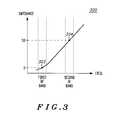
- FIG. 3shows the impedance transformation of the complex transformer as a function of frequency. This shows the transformation of the operative range of the transmitter in accordance with the preferred embodiment of the present invention.
- FIG. 4shows the frequency response of the first path in accordance with the preferred embodiment of the present invention.
- FIG. 5is a smith chart corresponding to the frequency response chart in FIG. 4, showing the impedance of the out of band and the in band signals in accordance with the preferred embodiment of the present invention.
- FIG. 6shows the frequency response of the second path of the preferred embodiment of the present invention.
- FIG. 7is a smith chart corresponding to the frequency response chart in FIG. 6, showing the impedance of the out of band and the in band signals in accordance with the preferred embodiment of the present invention.
- the present inventionprovides a unique method and apparatus for transmitting a radio frequency (RF) communication signal in multiple frequency bands.
- RFradio frequency
- Thismay be applicable in wireless communication devices that operate with multiple communication systems, such as cellular communication systems, personal communication systems (PCS), or satellite communication systems.
- a dual mode transceiver of a portable wireless radiotelephonetransmits RF communication signals in a first RF band attuned to what is typically referred to as the 800 MHz frequency band or cellular band, and a second RF band attuned to what is typically referred to as the 1900 MHz band, or PCS band.
- the dual mode transceiveris designed to operate under the advanced mobile phone system (AMPS) in the cellular band, or under the time division multiple access (TDMA) protocol in both the cellular band and the PCS bands.
- AMPSadvanced mobile phone system
- TDMAtime division multiple access
- the transceivermay be designed to operate under communication protocols other than AMPS and TDMA, such as the global system for mobile communications (GSM), code division multiple access (CDMA), cdma2000, W-CDMA and the like.
- GSMglobal system for mobile communications
- CDMAcode division multiple access
- cdma2000Code division multiple access
- W-CDMAWideband Code Division Multiple Access
- FIG. 1shows a wireless communication device 100 in accordance with the preferred embodiment of the present invention.
- This deviceis a cellular radiotelephone incorporating the present invention.
- a frame generator ASIC 102such as a CMOS ASIC available from Motorola, Inc.
- a microprocessor 104such as a 68HC11 microprocessor also available from Motorola, Inc., combine to generate the necessary communication protocol for operating in a cellular system.
- Microprocessor 104uses memory 106 comprising RAM 108 , EEPROM 110 , and ROM 112 , preferably consolidated in one package 114 , to execute the steps necessary to generate the protocol and to perform other functions for the wireless communication device, such as writing to a display 116 , accepting information from a keypad 118 , or controlling a frequency synthesizer 130 .
- ASIC 102processes audio transformed by audio circuitry 124 from a microphone 122 and to a speaker 126 .
- FIG. 1further shows the transmitter 128 which is capable of transmitting RF signals in two distinct RF bands which is required for operation of a dual mode communication device.
- FIG. 2shows a detailed illustration of the transmitter 128 portion of the wireless communication device.
- the transmitter 128is comprised of a power amplifier 200 , a complex transformer 202 , a first path 204 and a second path 206 .
- the first path 204is for transmitting in a first RF band and the second path 206 is for transmitting in a second RF band.
- the first path 204is attuned to transmit in accordance with the first operation mode and the second path 206 is attuned to transmit in accordance with the second operation mode.
- the first operation modetransmits AMPS RF communication signals, or in a low band
- the second operation modeis attuned to transmit PCS TDMA RF communication signals, or in a high band
- the AMPS communication systemoperates from 824 MHz to 894 MHz, which is subdivided into 30 kHz channels.
- the TDMA communication systemoperates in the 824 MHz to 894, for the cellular system, and from 1850 MHz to 1990 MHz subdivided into 30 kHz channels for the PCS system.
- the RF communication signalwill be
- the complex transformer 202is further comprised of a first node 210 , a second node 214 , a first transmission line 208 coupled between the PA 200 and the first node 210 , and a parallel capacitor 212 coupled between the first node 210 and the second node 214 .
- the second node 214is a common ground.
- the complex transformer 202is designed to fully transform the system characteristic impedance to the desired load target at the second RF band.
- the complex transformer 202partially transforms the impedance of the RF communication signal at the output of the PA 200 from a first impedance to a second impedance when the RF communication signal is in a first RF band.
- a chartshows the change in impedance by the complex transformer 202 over a given frequency range.
- the complex transformer 202completely transforms the RF communication signal from the first impedance to a third impedance when the RF communication signal is in a second RF band.
- the first impedance at the PA 200 outputis approximately two ohms and is partially transformed to approximately five ohms when the RF communication signal is in the first RF band and the first impedance is completely transformed from approximately two ohms to approximately fifty ohms when the RF communication signal is in the second RF band. Since the output impedance of the PA 200 is very low, a high quality (Q) first transmission line 208 is used followed by a high Q first capacitor 212 to ensure the circuit remains within the designed tolerances and operates properly.
- Qquality
- the first path 204is further comprised of: a third node 218 , a fourth node 224 , and a fifth node 230 , a second transmission line 216 coupled between the first node 210 and the third node 218 , a second parallel capacitor 220 coupled between the third node 218 and the second node 214 , a third transmission line coupled between the third node 218 and the fourth node 224 , a third parallel capacitor 226 , coupled between the fourth node and the second node, and a first filter 228 coupled between the fourth node 224 and the fifth node 230 .
- FIG. 4a frequency response chart shows the frequency response of the first path 204 .
- the frequency responseis such that the RF communication signals in the first RF band pass through to the antenna.
- FIG. 4also shows that the RF communication signal in the second RF band are attenuated significantly.
- FIG. 5is a smith chart 500 showing the first RF band impedance 402 of the first RF band or in the band RF communication signal, and the second RF band impedance 404 , of the second RF band or out of band communication signal.
- the second path 206is comprised of: a sixth node 238 , a seventh node 242 , a second filter 232 coupled between the first node 210 and the sixth node 238 , a fourth transmission line 240 coupled between the sixth node 238 and the seventh node 242 , a fourth parallel capacitor 244 coupled between the seventh node 242 and the second node 214 , and a third filter 246 coupled between the seventh node 242 and the fifth node 230 .
- FIG. 6a frequency response chart shows the frequency response of the second path 206 .
- the frequency responseis such that the RF communication signals in the second RF band pass through to the antenna.
- FIG. 6also shows that the RF communication signal in the first RF band are attenuated significantly.
- FIG. 7is a smith chart 500 showing the second RF band impedance 602 of the second RF band or in-band RF communication signal, and the first RF band impedance 604 , of the first RF band or out-of-band communication signal.
- the second filter 232is a capacitor 234 coupled in parallel with an inductor 236 coupled in series between the first node 210 and the sixth node 238 .
- the capacitor 234 coupled in parallel with inductor 236is commonly referred to as an LC tank.
- the second filter 232is parallel resonant at the first RF band and allows frequencies in the second RF band to pass through.
- the second filter 232is parallel resonant at 800 MHz acting as an open circuit.
- the second filter 232is above resonance and in the ideal component case would appear to be capacitive.
- the second filter 232actually appears as a through circuit at the second RF band, or the high band. Because the impedance of the RF communication signal in the second RF band is already transformed to the characteristic impedance at the first node, 50 ohms for example, the nominal Q values achieved with conventional components to form the fifth capacitor 234 and the parallel inductor 236 , cause very little dissipative loss. Using conventional components as opposed to high Q components and using only two components for the filter keeps the cost of the components low allowing the circuit to be economically feasible.
- the real portion of the impedance seen by the complex transformer 202 , looking into the second path 206 , or high band path,will be much higher than the impedance looking into the first path 204 . Because of this large impedance differential, only a small portion of the energy will be dissipated or lost in the second path 206 . This is accomplished by designing the complex transformer 202 so that the impedance of the RF communication signal is only partially transformed in the first RF band, or low band in the case of the preferred embodiment.
- the impedance of the second path 206is approximately 500 Ohms and the impedance of the first path 204 is 5 Ohms, resulting in an insertion loss of only three tenths of a dB, which is well within the insertion loss budget.
- the second transmission line 216 , third transmission line 222 , second capacitor 220 , and third capacitor 226 of the first pathare therefore designed to complete the impedance transformation from the second impedance at the first node 210 , to a fourth impedance at the fourth node 224 .
- the third capacitor 226has a value such that it is series resonant when the RF communication signal is in the second RF band, or high band. This eliminates the need to control or specify the out of band impedance of the first filter 228 . Any variations in load occurring after the third capacitor 226 are masked by the near zero impedance presented thereby at the second RF band.
Landscapes
- Engineering & Computer Science (AREA)
- Computer Networks & Wireless Communication (AREA)
- Signal Processing (AREA)
- Transmitters (AREA)
- Transceivers (AREA)
- Amplifiers (AREA)
Abstract
Description
Claims (13)
Priority Applications (8)
| Application Number | Priority Date | Filing Date | Title |
|---|---|---|---|
| US09/594,395US6389269B1 (en) | 2000-06-15 | 2000-06-15 | Method and apparatus for multiple band transmission |
| MXPA02012441AMXPA02012441A (en) | 2000-06-15 | 2001-06-13 | Method and apparatus for multiple band transmission. |
| AU2001268391AAU2001268391A1 (en) | 2000-06-15 | 2001-06-13 | Method and apparatus for multiple band transmission |
| CNB018110800ACN1223094C (en) | 2000-06-15 | 2001-06-13 | Method and apparatus for multi-band transmission |
| EP01946326AEP1305885B1 (en) | 2000-06-15 | 2001-06-13 | Method and apparatus for multiple band transmission |
| PCT/US2001/019030WO2001097389A2 (en) | 2000-06-15 | 2001-06-13 | Method and apparatus for multiple band transmission |
| KR10-2002-7017116AKR100470582B1 (en) | 2000-06-15 | 2001-06-13 | Method and apparatus for multiple band transmission |
| BR0111687-8ABR0111687A (en) | 2000-06-15 | 2001-06-13 | Method and apparatus for multiple band transmission |
Applications Claiming Priority (1)
| Application Number | Priority Date | Filing Date | Title |
|---|---|---|---|
| US09/594,395US6389269B1 (en) | 2000-06-15 | 2000-06-15 | Method and apparatus for multiple band transmission |
Publications (1)
| Publication Number | Publication Date |
|---|---|
| US6389269B1true US6389269B1 (en) | 2002-05-14 |
Family
ID=24378687
Family Applications (1)
| Application Number | Title | Priority Date | Filing Date |
|---|---|---|---|
| US09/594,395Expired - LifetimeUS6389269B1 (en) | 2000-06-15 | 2000-06-15 | Method and apparatus for multiple band transmission |
Country Status (8)
| Country | Link |
|---|---|
| US (1) | US6389269B1 (en) |
| EP (1) | EP1305885B1 (en) |
| KR (1) | KR100470582B1 (en) |
| CN (1) | CN1223094C (en) |
| AU (1) | AU2001268391A1 (en) |
| BR (1) | BR0111687A (en) |
| MX (1) | MXPA02012441A (en) |
| WO (1) | WO2001097389A2 (en) |
Cited By (21)
| Publication number | Priority date | Publication date | Assignee | Title |
|---|---|---|---|---|
| US20020132596A1 (en)* | 2001-01-20 | 2002-09-19 | Samsung Electronics Co.,Ltd. | Power rate enhancement circuit for an RF power amplifier in a dual mode mobile phone |
| US20040066860A1 (en)* | 2002-10-08 | 2004-04-08 | Bois Karl Joseph | Passive redundant digital data receiver with dual comparator edge detection |
| US20040087292A1 (en)* | 2002-10-31 | 2004-05-06 | Shiu Da-Shan | Low latency frequency switching |
| US20050182683A1 (en)* | 2004-02-12 | 2005-08-18 | Steven Tischer | Systems, methods, and a storage medium for obtaining an offer for a sale of a product or a service |
| US20050245202A1 (en)* | 2004-04-30 | 2005-11-03 | Nokia Corporation | Versatile antenna switch architecture |
| US20050245201A1 (en)* | 2004-04-30 | 2005-11-03 | Nokia Corporation | Front-end topology for multiband multimode communication engines |
| US20090111401A1 (en)* | 2007-10-29 | 2009-04-30 | Grigory Itkin | Transmitter arrangement |
| US20090225873A1 (en)* | 2008-03-05 | 2009-09-10 | Qualcomm Incorporated | Multiple Transmitter System and Method |
| US20090243752A1 (en)* | 2008-03-28 | 2009-10-01 | Min-Shun Hsu | Compact Diplexer |
| US20100137023A1 (en)* | 2007-03-28 | 2010-06-03 | Kyocera Corporation | Mobile Communication Terminal and Control Method Thereof |
| US7835712B1 (en)* | 2006-12-19 | 2010-11-16 | Palm, Inc. | Apparatus and methods for providing multi-band operation in a mobile computing device |
| US20100297968A1 (en)* | 2009-05-19 | 2010-11-25 | Poh Boon Leong | Circuits and methods for combining signal power |
| US20100308933A1 (en)* | 2009-06-03 | 2010-12-09 | Qualcomm Incorporated | Tunable matching circuits for power amplifiers |
| US20100321086A1 (en)* | 2009-06-19 | 2010-12-23 | Qualcomm Incorporated | Power and impedance measurement circuits for a wireless communication device |
| US20110018632A1 (en)* | 2009-07-24 | 2011-01-27 | Qualcomm Incorporated | Power amplifier with switched output matching for multi-mode operation |
| US20110043956A1 (en)* | 2009-08-19 | 2011-02-24 | Qualcomm Incorporated | Protection circuit for power amplifier |
| US20130309985A1 (en)* | 2011-01-28 | 2013-11-21 | Murata Manufacturing Co., Ltd. | Transmission module |
| US20140111275A1 (en)* | 2012-10-19 | 2014-04-24 | Rf Micro Devices, Inc. | Efficient power transfer power amplifier (pa) architecture |
| US9000847B2 (en) | 2009-08-19 | 2015-04-07 | Qualcomm Incorporated | Digital tunable inter-stage matching circuit |
| US9220067B2 (en) | 2011-05-02 | 2015-12-22 | Rf Micro Devices, Inc. | Front end radio architecture (FERA) with power management |
| US20200403646A1 (en)* | 2018-03-01 | 2020-12-24 | Murata Manufacturing Co., Ltd. | Radio-frequency module and communication device |
Families Citing this family (3)
| Publication number | Priority date | Publication date | Assignee | Title |
|---|---|---|---|---|
| JP5086630B2 (en)* | 2006-12-20 | 2012-11-28 | 株式会社エヌ・ティ・ティ・ドコモ | Matching circuit, dual-band power amplifier |
| US8369796B2 (en)* | 2006-12-22 | 2013-02-05 | Intel Corporation | Multi-band tunable frequency reconfigurable antennas using higher order resonances |
| US7917170B2 (en)* | 2008-03-13 | 2011-03-29 | Kyocera Corporation | Multiple-band radio frequency (RF) circuit and method for a wireless communication device |
Citations (8)
| Publication number | Priority date | Publication date | Assignee | Title |
|---|---|---|---|---|
| US4037177A (en)* | 1976-03-03 | 1977-07-19 | Tyrey Elasco A | Radio-frequency coupler |
| US5020092A (en) | 1989-06-23 | 1991-05-28 | Motorola, Inc. | Dual-bandwidth cellular telephone |
| US5060294A (en) | 1990-07-05 | 1991-10-22 | Motorola, Inc. | Dual mode power amplifier for radiotelephone |
| US5251331A (en) | 1992-03-13 | 1993-10-05 | Motorola, Inc. | High efficiency dual mode power amplifier apparatus |
| US5438684A (en) | 1992-03-13 | 1995-08-01 | Motorola, Inc. | Radio frequency signal power amplifier combining network |
| US6023611A (en)* | 1997-02-25 | 2000-02-08 | Telefonaktiebolaget Lm Ericsson | Filter device for suppressing harmonics in radio frequency signals when dual frequencies exist |
| US6091966A (en)* | 1997-09-29 | 2000-07-18 | Ericsson, Inc. | Dual-band, dual-mode power amplifier |
| US6188877B1 (en)* | 1997-07-03 | 2001-02-13 | Ericsson Inc. | Dual-band, dual-mode power amplifier with reduced power loss |
Family Cites Families (1)
| Publication number | Priority date | Publication date | Assignee | Title |
|---|---|---|---|---|
| US5969582A (en)* | 1997-07-03 | 1999-10-19 | Ericsson Inc. | Impedance matching circuit for power amplifier |
- 2000
- 2000-06-15USUS09/594,395patent/US6389269B1/ennot_activeExpired - Lifetime
- 2001
- 2001-06-13MXMXPA02012441Apatent/MXPA02012441A/enactiveIP Right Grant
- 2001-06-13KRKR10-2002-7017116Apatent/KR100470582B1/ennot_activeExpired - Fee Related
- 2001-06-13AUAU2001268391Apatent/AU2001268391A1/ennot_activeAbandoned
- 2001-06-13BRBR0111687-8Apatent/BR0111687A/enactiveSearch and Examination
- 2001-06-13EPEP01946326Apatent/EP1305885B1/ennot_activeExpired - Lifetime
- 2001-06-13WOPCT/US2001/019030patent/WO2001097389A2/enactiveIP Right Grant
- 2001-06-13CNCNB018110800Apatent/CN1223094C/ennot_activeExpired - Fee Related
Patent Citations (8)
| Publication number | Priority date | Publication date | Assignee | Title |
|---|---|---|---|---|
| US4037177A (en)* | 1976-03-03 | 1977-07-19 | Tyrey Elasco A | Radio-frequency coupler |
| US5020092A (en) | 1989-06-23 | 1991-05-28 | Motorola, Inc. | Dual-bandwidth cellular telephone |
| US5060294A (en) | 1990-07-05 | 1991-10-22 | Motorola, Inc. | Dual mode power amplifier for radiotelephone |
| US5251331A (en) | 1992-03-13 | 1993-10-05 | Motorola, Inc. | High efficiency dual mode power amplifier apparatus |
| US5438684A (en) | 1992-03-13 | 1995-08-01 | Motorola, Inc. | Radio frequency signal power amplifier combining network |
| US6023611A (en)* | 1997-02-25 | 2000-02-08 | Telefonaktiebolaget Lm Ericsson | Filter device for suppressing harmonics in radio frequency signals when dual frequencies exist |
| US6188877B1 (en)* | 1997-07-03 | 2001-02-13 | Ericsson Inc. | Dual-band, dual-mode power amplifier with reduced power loss |
| US6091966A (en)* | 1997-09-29 | 2000-07-18 | Ericsson, Inc. | Dual-band, dual-mode power amplifier |
Cited By (43)
| Publication number | Priority date | Publication date | Assignee | Title |
|---|---|---|---|---|
| US6950637B2 (en)* | 2001-01-20 | 2005-09-27 | Samsung Electronics Co., Ltd. | Power rate enhancement circuit for an RF power amplifier in a dual mode mobile phone |
| US20020132596A1 (en)* | 2001-01-20 | 2002-09-19 | Samsung Electronics Co.,Ltd. | Power rate enhancement circuit for an RF power amplifier in a dual mode mobile phone |
| US20040066860A1 (en)* | 2002-10-08 | 2004-04-08 | Bois Karl Joseph | Passive redundant digital data receiver with dual comparator edge detection |
| US7136429B2 (en)* | 2002-10-08 | 2006-11-14 | Hewlett-Packard Development Company, Lp. | Passive redundant digital data receiver with dual comparator edge detection |
| US7307480B2 (en)* | 2002-10-31 | 2007-12-11 | Qualcomm Incorporated | Low latency frequency switching |
| US20040087292A1 (en)* | 2002-10-31 | 2004-05-06 | Shiu Da-Shan | Low latency frequency switching |
| US8565121B2 (en) | 2002-10-31 | 2013-10-22 | Qualcomm, Incorporated | Low latency frequency switching |
| US20080212553A1 (en)* | 2002-10-31 | 2008-09-04 | Qualcomm Incorporated | Low latency frequency switching |
| US20080222008A1 (en)* | 2004-02-12 | 2008-09-11 | Bellsouth Intellectual Property Corporation | Systems, Methods, And A Storage Medium For Obtaining An Offer For A Sale Of A Product Or A Service |
| US7379904B2 (en)* | 2004-02-12 | 2008-05-27 | At&T Delaware Intellectual Property, Inc. | Method and storage medium for obtaining an offer for a sale of a product or a service |
| US20050182683A1 (en)* | 2004-02-12 | 2005-08-18 | Steven Tischer | Systems, methods, and a storage medium for obtaining an offer for a sale of a product or a service |
| US8417586B2 (en) | 2004-02-12 | 2013-04-09 | At&T Intellectual Property I, L.P. | Systems, methods, and a storage medium for obtaining an offer for a sale of a product or a service |
| US7187945B2 (en)* | 2004-04-30 | 2007-03-06 | Nokia Corporation | Versatile antenna switch architecture |
| US20050245201A1 (en)* | 2004-04-30 | 2005-11-03 | Nokia Corporation | Front-end topology for multiband multimode communication engines |
| US20050245202A1 (en)* | 2004-04-30 | 2005-11-03 | Nokia Corporation | Versatile antenna switch architecture |
| US7835712B1 (en)* | 2006-12-19 | 2010-11-16 | Palm, Inc. | Apparatus and methods for providing multi-band operation in a mobile computing device |
| US8041321B1 (en)* | 2006-12-19 | 2011-10-18 | Hewlett-Packard Development Company, L.P. | Apparatus and methods for providing multi-band operation in a mobile computing device |
| US8437809B2 (en)* | 2007-03-28 | 2013-05-07 | Kyocera Corporation | Mobile communication terminal and control method thereof |
| US20100137023A1 (en)* | 2007-03-28 | 2010-06-03 | Kyocera Corporation | Mobile Communication Terminal and Control Method Thereof |
| US7853290B2 (en)* | 2007-10-29 | 2010-12-14 | Infineon Technologies Ag | Transmitter arrangement |
| US20090111401A1 (en)* | 2007-10-29 | 2009-04-30 | Grigory Itkin | Transmitter arrangement |
| US20090225873A1 (en)* | 2008-03-05 | 2009-09-10 | Qualcomm Incorporated | Multiple Transmitter System and Method |
| US20090243752A1 (en)* | 2008-03-28 | 2009-10-01 | Min-Shun Hsu | Compact Diplexer |
| US7876175B2 (en)* | 2008-03-28 | 2011-01-25 | Ralink Technology Corp. | Compact diplexer |
| US8594594B2 (en)* | 2009-05-19 | 2013-11-26 | Marvell World Trade Ltd. | Circuits and methods for combining signal power |
| TWI458174B (en)* | 2009-05-19 | 2014-10-21 | Marvell World Trade Ltd | Circuits and methods combining signal power |
| US9368857B2 (en) | 2009-05-19 | 2016-06-14 | Marvell World Trade Ltd. | Combining signal power using magnetic coupling between conductors |
| US20100297968A1 (en)* | 2009-05-19 | 2010-11-25 | Poh Boon Leong | Circuits and methods for combining signal power |
| US9143172B2 (en) | 2009-06-03 | 2015-09-22 | Qualcomm Incorporated | Tunable matching circuits for power amplifiers |
| US20100308933A1 (en)* | 2009-06-03 | 2010-12-09 | Qualcomm Incorporated | Tunable matching circuits for power amplifiers |
| US8963611B2 (en) | 2009-06-19 | 2015-02-24 | Qualcomm Incorporated | Power and impedance measurement circuits for a wireless communication device |
| US20100321086A1 (en)* | 2009-06-19 | 2010-12-23 | Qualcomm Incorporated | Power and impedance measurement circuits for a wireless communication device |
| US20110018632A1 (en)* | 2009-07-24 | 2011-01-27 | Qualcomm Incorporated | Power amplifier with switched output matching for multi-mode operation |
| US8750810B2 (en)* | 2009-07-24 | 2014-06-10 | Qualcomm Incorporated | Power amplifier with switched output matching for multi-mode operation |
| US9000847B2 (en) | 2009-08-19 | 2015-04-07 | Qualcomm Incorporated | Digital tunable inter-stage matching circuit |
| US20110043956A1 (en)* | 2009-08-19 | 2011-02-24 | Qualcomm Incorporated | Protection circuit for power amplifier |
| US9559639B2 (en) | 2009-08-19 | 2017-01-31 | Qualcomm Incorporated | Protection circuit for power amplifier |
| US20130309985A1 (en)* | 2011-01-28 | 2013-11-21 | Murata Manufacturing Co., Ltd. | Transmission module |
| US9220067B2 (en) | 2011-05-02 | 2015-12-22 | Rf Micro Devices, Inc. | Front end radio architecture (FERA) with power management |
| US9071210B2 (en)* | 2012-10-19 | 2015-06-30 | Rf Micro Devices, Inc. | Efficient power transfer power amplifier (PA) architecture |
| US20140111275A1 (en)* | 2012-10-19 | 2014-04-24 | Rf Micro Devices, Inc. | Efficient power transfer power amplifier (pa) architecture |
| US20200403646A1 (en)* | 2018-03-01 | 2020-12-24 | Murata Manufacturing Co., Ltd. | Radio-frequency module and communication device |
| US11817890B2 (en)* | 2018-03-01 | 2023-11-14 | Murata Manufacturing Co., Ltd. | Radio-frequency module and communication device |
Also Published As
| Publication number | Publication date |
|---|---|
| EP1305885A4 (en) | 2006-01-18 |
| WO2001097389A2 (en) | 2001-12-20 |
| EP1305885A2 (en) | 2003-05-02 |
| WO2001097389A3 (en) | 2002-05-30 |
| EP1305885B1 (en) | 2012-05-30 |
| BR0111687A (en) | 2003-07-01 |
| CN1436404A (en) | 2003-08-13 |
| MXPA02012441A (en) | 2003-06-06 |
| AU2001268391A1 (en) | 2001-12-24 |
| KR20030010726A (en) | 2003-02-05 |
| KR100470582B1 (en) | 2005-03-10 |
| CN1223094C (en) | 2005-10-12 |
Similar Documents
| Publication | Publication Date | Title |
|---|---|---|
| US6389269B1 (en) | Method and apparatus for multiple band transmission | |
| US7567782B2 (en) | Re-configurable impedance matching and harmonic filter system | |
| EP1604509B1 (en) | Load variation tolerant radio frequency (rf) amplifier | |
| US7706835B2 (en) | High-frequency circuit device | |
| US20040106389A1 (en) | Mobile phone and related method for matching antenna with different matching circuits for different bands | |
| US8509718B2 (en) | Broadband receive only tuner combined with receive switch | |
| US20070132511A1 (en) | Gain adjusting and circuit arrangement | |
| US20070218844A1 (en) | Transmitter, power amplifier and filtering method | |
| US6510310B1 (en) | Dual mode phone architecture utilizing a single transmit-receive switch | |
| KR20010106398A (en) | High-frequency power amplifier module | |
| US6798294B2 (en) | Amplifier with multiple inputs | |
| WO2001005028A1 (en) | A dual-band, dual-mode power amplifier | |
| CN111819791B (en) | Multiplexer, high frequency front end circuit and communication device | |
| US20030045252A1 (en) | Power amplifier | |
| US7054600B2 (en) | Channel-selective amplifier with tunable filter | |
| KR100652899B1 (en) | Direct Conversion RF Front-End Transceivers and Their Components | |
| JP2011155357A (en) | Multi-band power amplifier | |
| US8023999B2 (en) | Base station architecture using decentralized duplexers | |
| US20140254568A1 (en) | Semiconductor module | |
| JP2002016448A (en) | Radio frequency amplifier circuit and receiving chain circuit | |
| JP2001127652A (en) | High frequency radio equipment | |
| JP2008300933A (en) | Amplifier circuit and wireless communication device using the same | |
| WO2011092910A1 (en) | Power amplifier | |
| WO2003103156A2 (en) | A radio frequency circuit |
Legal Events
| Date | Code | Title | Description |
|---|---|---|---|
| AS | Assignment | Owner name:MOTOROLA, INC., ILLINOIS Free format text:ASSIGNMENT OF ASSIGNORS INTEREST;ASSIGNORS:NANNI, PETER;XIANG, LI;MIDLOCK, ERIC;REEL/FRAME:010934/0475 Effective date:20000614 | |
| STCF | Information on status: patent grant | Free format text:PATENTED CASE | |
| FPAY | Fee payment | Year of fee payment:4 | |
| FPAY | Fee payment | Year of fee payment:8 | |
| AS | Assignment | Owner name:MOTOROLA MOBILITY, INC, ILLINOIS Free format text:ASSIGNMENT OF ASSIGNORS INTEREST;ASSIGNOR:MOTOROLA, INC;REEL/FRAME:025673/0558 Effective date:20100731 | |
| AS | Assignment | Owner name:MOTOROLA MOBILITY LLC, ILLINOIS Free format text:CHANGE OF NAME;ASSIGNOR:MOTOROLA MOBILITY, INC.;REEL/FRAME:029216/0282 Effective date:20120622 | |
| FPAY | Fee payment | Year of fee payment:12 | |
| AS | Assignment | Owner name:GOOGLE TECHNOLOGY HOLDINGS LLC, CALIFORNIA Free format text:ASSIGNMENT OF ASSIGNORS INTEREST;ASSIGNOR:MOTOROLA MOBILITY LLC;REEL/FRAME:034500/0001 Effective date:20141028 |