US6385672B1 - System to optimize packet buffer utilization via selectively partitioned transmit and receive buffer portions - Google Patents
System to optimize packet buffer utilization via selectively partitioned transmit and receive buffer portionsDownload PDFInfo
- Publication number
- US6385672B1 US6385672B1US08/879,406US87940697AUS6385672B1US 6385672 B1US6385672 B1US 6385672B1US 87940697 AUS87940697 AUS 87940697AUS 6385672 B1US6385672 B1US 6385672B1
- Authority
- US
- United States
- Prior art keywords
- pointer
- read
- write
- packet
- buffer
- Prior art date
- Legal status (The legal status is an assumption and is not a legal conclusion. Google has not performed a legal analysis and makes no representation as to the accuracy of the status listed.)
- Expired - Fee Related
Links
Images


Classifications
- H—ELECTRICITY
- H04—ELECTRIC COMMUNICATION TECHNIQUE
- H04L—TRANSMISSION OF DIGITAL INFORMATION, e.g. TELEGRAPHIC COMMUNICATION
- H04L49/00—Packet switching elements
- H04L49/90—Buffering arrangements
- H04L49/9084—Reactions to storage capacity overflow
- H04L49/9089—Reactions to storage capacity overflow replacing packets in a storage arrangement, e.g. pushout
- G—PHYSICS
- G06—COMPUTING OR CALCULATING; COUNTING
- G06F—ELECTRIC DIGITAL DATA PROCESSING
- G06F5/00—Methods or arrangements for data conversion without changing the order or content of the data handled
- G06F5/06—Methods or arrangements for data conversion without changing the order or content of the data handled for changing the speed of data flow, i.e. speed regularising or timing, e.g. delay lines, FIFO buffers; over- or underrun control therefor
- G06F5/10—Methods or arrangements for data conversion without changing the order or content of the data handled for changing the speed of data flow, i.e. speed regularising or timing, e.g. delay lines, FIFO buffers; over- or underrun control therefor having a sequence of storage locations each being individually accessible for both enqueue and dequeue operations, e.g. using random access memory
- G06F5/12—Means for monitoring the fill level; Means for resolving contention, i.e. conflicts between simultaneous enqueue and dequeue operations
- G06F5/14—Means for monitoring the fill level; Means for resolving contention, i.e. conflicts between simultaneous enqueue and dequeue operations for overflow or underflow handling, e.g. full or empty flags
- H—ELECTRICITY
- H04—ELECTRIC COMMUNICATION TECHNIQUE
- H04L—TRANSMISSION OF DIGITAL INFORMATION, e.g. TELEGRAPHIC COMMUNICATION
- H04L49/00—Packet switching elements
- H04L49/90—Buffering arrangements
- H—ELECTRICITY
- H04—ELECTRIC COMMUNICATION TECHNIQUE
- H04L—TRANSMISSION OF DIGITAL INFORMATION, e.g. TELEGRAPHIC COMMUNICATION
- H04L49/00—Packet switching elements
- H04L49/90—Buffering arrangements
- H04L49/901—Buffering arrangements using storage descriptor, e.g. read or write pointers
- G—PHYSICS
- G06—COMPUTING OR CALCULATING; COUNTING
- G06F—ELECTRIC DIGITAL DATA PROCESSING
- G06F2205/00—Indexing scheme relating to group G06F5/00; Methods or arrangements for data conversion without changing the order or content of the data handled
- G06F2205/10—Indexing scheme relating to groups G06F5/10 - G06F5/14
- G06F2205/102—Avoiding metastability, i.e. preventing hazards, e.g. by using Gray code counters
- G—PHYSICS
- G06—COMPUTING OR CALCULATING; COUNTING
- G06F—ELECTRIC DIGITAL DATA PROCESSING
- G06F2205/00—Indexing scheme relating to group G06F5/00; Methods or arrangements for data conversion without changing the order or content of the data handled
- G06F2205/10—Indexing scheme relating to groups G06F5/10 - G06F5/14
- G06F2205/108—Reading or writing the data blockwise, e.g. using an extra end-of-block pointer
Definitions
- the present inventionrelates to a device for connecting a computer system to a packet-switched data network, such and more particularly to the design of a system that optimizes utilization of a packet buffer within the device for storing packets in transit between the computer system and the packet-switched data network.
- a transmit bufferfor storing data from the computer system to be transmitted onto the data network
- a receive bufferfor receiving data from the data network to be transmitted to the computer system.
- buffer overrunoccurs when the buffer becomes overly full before packets can be removed from the buffer.
- Buffer underrunoccurs when the buffer becomes empty and data continues to be transmitted from the empty buffer.
- transmit and receive buffersare typically controlled by a controller, which can take the form of a microprocessor.
- a microprocessor-based controllercan access packets in the transmit and the receive buffers using memory mapping which has the advantage that data in the buffers can be flexibly accessed.
- the speed of accesses to the bufferare limited by the microprocessor speed, and hence can be relatively slow.
- Microprocessorscan also be quite expensive, adding significantly to the cost of a network interface card (NIC).
- NICnetwork interface card
- Network interface devicesare typically implemented using separate transmit and receive buffers, which are of a fixed size that cannot be varied to meet the requirements of different buses, data networks and network traffic patterns.
- What is neededis a system for flexibly allocating buffer memory in a network interface device between transmit and receive buffers in order to optimize performance for the network interface device across a wide range of buses, data networks and network usage patterns.
- the present inventionprovides a device which facilitates communications between a computer system and a data network by buffering data in transit between the computer system and the data network in a single buffer memory which can be flexibly partitioned into separate transmit and receive buffers.
- This flexible partitioningallows the relative sizes of the transmit and receive buffers to be optimized across a wide range of buses, data networks and network usage patterns.
- the transmit and receive buffersare structured as ring buffers within respectively allocated portions of the buffer memory.
- the buffer memoryis controlled by a simple finite state machine controller, which is free from the performance impediments and higher cost associated with a microprocessor-based controller.
- the present inventionalso provides support for retransmission of packets that encounter transmission problems such as collisions during transmissions on the data network.
- the present inventionadditionally provides the ability to discard incomplete packets.
- One embodiment of the present inventionis an apparatus for transmitting data between a first communication channel and a second communication channel.
- the apparatuscomprises a first interface, coupled to the first communication channel, and a second interface coupled to the second communication channel.
- the apparatusalso includes a buffer memory, coupled to the first communication channel and the second communication channel, the buffer memory being selectively partitionable so that a portion of the buffer memory of selectable size is allocated to a transmit buffer for buffering data to be transmitted on the first communication channel, and a portion of the buffer is allocated to a receive buffer of selectable size for buffering data received from the first communication channel.
- the apparatusalso includes a controller, coupled to the buffer memory, for controlling data flowing through the transmit buffer and the receive buffer.
- the controllerdoes not include a microprocessor.
- the apparatusincludes a plurality of pointer registers coupled to the buffer memory, for storing pointers for accessing the transmit and receive buffers, and at least one logic circuit coupled to the plurality of registers, for performing arithmetic operations on the plurality of pointer values stored in the plurality of pointer registers.
- One embodimentis an apparatus for buffering packet data in first in first out order, comprising: a buffer; a write pointer coupled to the buffer, for pointing to a location where packet data is being written into the buffer; a start of a read packet pointer coupled to the buffer, for pointing to the start of a read packet being read from the buffer, and a read pointer coupled to the buffer, for pointing to a location where packet data is being read from the packet being read, the read pointer being resettable to point back to a location stored in the start of read packet pointer to facilitate retransmission of the read packet when a transmission error takes place.
- the apparatusincludes a start of write packet pointer coupled to the buffer, for pointing to the start of the packet being written into the buffer. It also includes resources coupled to the write pointer, for resetting the write pointer to point back to a location stored in the start of write packet pointer, to facilitate discarding of an incomplete packet.
- the apparatusincludes an end of read packet pointer, coupled to the buffer, for pointing to the end of a packet being read; and resources coupled to the read pointer, for comparing the read pointer with the end of read packet pointer, to determine when the packet is completely read.
- Another embodimentis as an apparatus for performing pointer arithmetic for a pointer into a buffer, the pointer arithmetic including a pointer incrementing operation that increments a first pointer until it reaches a selectable maximum value and then returns to a starting value, comprising: a first pointer input, for receiving the first pointer; a selectable maximum value input, for indicating a selectable maximum value of the output for purposes of setting the output to the starting value during a pointer increment operation that exceeds the selectable maximum value; an output, for outputting the result of a pointer arithmetic operation, and a logic circuit, coupled to the first input, the selectable maximum value input and the output, which includes circuitry that increments the first pointer to produce the output, such that if the value of the first pointer after incrementing exceeds the selectable maximum value, the output is set to the starting value.
- the apparatusincludes a second pointer input coupled to the logic circuit, for receiving one of a second pointer value and an operand, wherein the logic circuit includes circuitry to perform an operation between the first pointer input and the second pointer input to produce the output.
- FIG. 1is a block diagram illustrating some of the major functional components of a device for connecting a computer system to a packet-switched data network in accordance with an aspect of the present invention.
- FIG. 2is a diagram illustrating how memory 200 is partitioned between receive buffer 123 and transmit buffer 124 in accordance with an aspect of the present invention.
- FIG. 3is a diagram illustrating the structure of a buffer in accordance with an aspect of the present invention.
- FIG. 4presents a number of computations involved in pointer operations in accordance with an aspect of the present invention.
- FIG. 5is a block diagram illustrating an ALU and associated circuitry for a write pointer in accordance with an aspect of the present invention.
- FIG. 6is a diagram illustrating the operands involved in computations for in the circuitry illustrated in FIG. 5 in accordance with an aspect of the present invention.
- FIG. 7is a block diagram of some of the major functional components of circuitry for performing arithmetic operations on a read pointer in accordance with an aspect of the present invention.
- FIG. 8illustrates the operands involved in the operations carried out by the circuitry in FIG. 7 in accordance with an aspect of the present invention.
- FIG. 9is a circuit diagram of an arithmetic logic unit for performing pointer operations, including an increment operation for a buffer of selectable size, in accordance with an aspect of the present invention.
- FIG. 10is a circuit diagram illustrating an optimized carry lookahead circuit for an arithmetic logic unit in accordance with an aspect of the present invention.
- FIG. 11presents possible configurations for the arithmetic logic unit illustrated in FIG. 9 in accordance with an aspect of the present invention.
- FIG. 12is a circuit diagram of the architecture of the buffer memory in accordance with an aspect of the present invention.
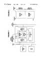
- FIG. 1is a block diagram illustrating some of the major functional components of a device for connecting a computer system to a data network in accordance with an aspect of the present invention.
- the computer systemcomprises CPU 104 which is linked to memory 102 through bus 100 .
- CPU 104may be any type of central processing unit, including a device controller, a microprocessor or a mainframe computer system.
- Memory 102is any type of memory device including a random access memory and a magnetic storage device.
- Bus 100is any type of bus that can be used to connect computer system components together, including peripheral component interconnect (PCI), extent industry-standard architecture (EISA), and industry standard architecture (ISA) buses.
- Bus 100connects to data network 110 through network interface card 120 .
- PCIperipheral component interconnect
- EISAextent industry-standard architecture
- ISAindustry standard architecture
- Data network 110is any type of packet-switched data network, including Ethernet, token ring, and fiber distributed data interface (FDDI) networks.
- EthernetEthernet
- token ringtoken ring
- FDDIfiber distributed data interface
- Network interface card (NIC) 120includes bus interface 121 , receive buffer 123 , media access control (MAC) interface 122 , transmit buffer 124 and controller 125 .
- Bus interface 121is coupled to bus 100 , and provides bus interface functions for communications across bus 100 .
- Bus interface 121is coupled to transmit buffer 124 and receive buffer 123 , and data flows between bus 100 and buffers 123 and 124 through bus interface 121 .
- Receive buffer 123 and transmit buffer 124comprise memory 200 .
- MAC interface 122is coupled to data network 110 , and it provides MAC layer interface functions for communications across data network 110 .
- MAC interface 122additionally connects to transmit buffer 124 , to which it writes data, and also connects to receive buffer 123 from which it reads data.
- Controller 125is coupled to bus interface 121 , memory 200 and MAC interface 122 . Controller 125 coordinates the activities of bus interface 121 , memory 200 and MAC interface 122 in such a way as to facilitate the transfer of data between bus 100 and data network 110 .
- controller 125is a DMA device, which is capable of writing to and reading from memory 102 across bus interface 121 and bus 100 .
- controller 125is implemented using a standard cell ASIC, and does not include a microprocessor.
- the circuit illustrated in FIG. 1generally operates as follows.
- datais transferred from memory 102 through bus 100 and bus interface 121 to transmit buffer 124 within memory 200 . This transfer is accomplished either by CPU 104 , or alternatively by the DMA circuitry within controller 125 .
- Data within transmit buffer 124is then transmitted through MAC interface 122 and data network 110 to an ultimate destination on a remote host coupled to data network 110 .
- datais received from data network 110 through MAC interface 122 into receiver buffer 123 .
- Datais then transferred from receiver buffer 123 through bus interface 121 and bus 100 into memory 102 under control of controller 125 .
- data transferred between bus 100 and data network 110is in the form of packets, including a header portion containing addressing information, and a data portion containing the data to be transferred.
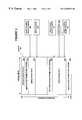
- FIG. 2is a diagram illustrating how memory 200 is partitioned between receive buffer 123 and transmit buffer 124 in accordance with an aspect of the present invention.
- receive buffer 123begins at address 000 and proceeds through increasing addresses to the boundary between receive buffer 123 and transmit buffer 124 .
- transmit buffer 124starts at a “last” address of memory 200 and proceeds through decreasing addresses to the boundary between transmit buffer 124 and receive buffer 123 .
- Memory 200is selectively partitionable between receive buffer 123 and transmit buffer 124 along block boundaries.
- memory 200can be partitioned so that receive buffer 123 and transmit buffer 124 are allocated in the following proportions: (2K, 6K), (3K, 5K), (4K, 4K), (5K, 3K) and (6K, 2K).
- the partitioning that is desiredis selected either using a hardware jumper or through software at system boot up time.
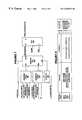
- FIG. 3is a diagram illustrating the structure of a buffer including the various pointers used to access the buffer in accordance with an aspect of the present invention.
- Buffer 300contains previous write packet 302 , write packet frame start header 312 , write packet data 314 , read packet frame start header 324 , read packet data 326 and next read packet frame start header 328 .
- Write packet frame start header 312 and write packet data 314comprise a write packet, which is the current packet being written to in buffer 300 .
- Read packet frame start header 324 and read packet data 326comprise a read packet, which is a packet presently being read from in buffer 300 . Note that a frame start header portion of a packet contains addressing and control information, whereas a data portion of a packet contains the actual data to be transmitted in the packet.
- Buffer 300is accessed through a plurality of pointers, including start of write packet pointer 310 , write pointer 316 , start of read packet pointer 320 , read pointer 322 and end of read packet pointer 329 .
- Write pointer 316points to the location where data is currently being written to within buffer 300 .
- write pointer 316is reset so that it points to a location contained within start of write packet pointer 310 , so that write pointer 316 points to the beginning of write packet frame start header 312 . In this way, a packet that is received in improper form is discarded.
- Read pointer 322points to a location within read packet data 326 where data is currently being read from buffer 300 . When a transmission error occurs, read pointer 322 is reset so that it points to a location contained within start of read packet pointer 320 . Start of read packet pointer 320 points to the beginning of the data portion of a packet currently being read. In this way, read pointer 322 can be reset so that retransmission of the data within the packet currently being read can take place without having to retrieve the data again from its source. Read pointer 322 proceeds through read packet data 326 until the value contained within read pointer 322 matches the value contained in end of read packet pointer 329 . End of read packet pointer 329 points to the end of the packet currently being read.
- the pointersare constrained in a number of ways.
- Write pointer 316cannot proceed past the location of read pointer 322 . Otherwise, a buffer overflow will occur.
- read pointer 322cannot proceed past the location of write pointer 316 . Otherwise, a buffer underrun will take place.
- FIG. 4illustrates some of the control codes and values used in pointer computations in accordance with an aspect of the present invention.
- the left hand columnindicates the options for memory sizes which are specified by memsize[ 1 : 0 ].
- An 8K buffer memoryis specified by 00.
- a 32K buffer memoryis specified by 01.
- a 64K buffer memoryis specified by 10.
- a 128K buffer memoryis specified by 11.
- An 8K buffer memorycan be partitioned in the following ways: (2K:6K), (3K:5K), (4K:4K), (5K:3K) and ( 6 K: 2 K). Only one possible partitioning of a 32K buffer is allowed, (16K:16K). Five partitionings of a 64K buffer are allowed, these are: (16K:48K), (24K:40K), (32K:3K), (40K:24K) and (48K:16K). Only one partitioning of a 128K memory is possible, (64K:64K).
- the next columnindicates the maximum free space that is allowed for each possible partitioning. This number is simply the partition size minus one.
- the next and last columnindicates a mask value to be used in a computation for the BufUsedSpace. This mask value is used to mask out the extraneous high order bits of a particular partition size.
- FIG. 5is a circuit diagram illustrating the logic involved in performing pointer operations in accordance with an aspect of the present invention.
- FIG. 5includes operand A multiplexer (MUX) 500 , operand B MUX 510 , carry in 520 , pointer arithmetic and logic unit (ALU) 530 and D-FF 540 .
- Pointer ALU 530performs operations on pointers, including addition.
- Pointer ALU 530is connected to, and takes inputs from, operand A MUX 500 and operand B MUX 510 .
- Pointer ALU 530is additionally connected to, and takes an input from, carry in 520 .
- Pointer ALUproduces an output which feeds into inputs of Dflip-flop (D-FF).
- D-FFDflip-flop
- Function code signal 550feeds into, and controls the operation of, carry in 520 , operand A MUX 500 and operand B MUX 510 .
- Function code signal 550selectively switches operand A MUX 500 between (start of write packet pointer[ 18 : 2 ], 11 ) and write pointer[ 18 : 0 ].
- Operand B MUX 510selectively switches the B input of Pointer ALU 530 between ( ⁇ start of write packet pointer[ 18 : 2 ], 00 ) and -write pointer[ 1 : 0 ], one and three.
- Function code signal 550selectively switches carry in 520 between zero and one.
- D-FF 540which is a bank of D flip-flops for storing the output of pointer ALU 530 .
- D-FF 540includes a loadW input and clock input. When these are asserted, it produces an output which is a new value for the write pointer.
- FIG. 6lists some of the operations performed by the logic illustrated in FIG. 5 in accordance with an aspect of the present invention.
- the Wplus 1 operationtakes as input the write pointer and a one value, and outputs write pointer+1.
- the operation Wplus 4takes as input the write pointer, a value three and a carry in, and outputs the write pointer+4.
- the alignW operationtakes as input the write pointer and subtracts from the write pointer the lower-most two bits of the write pointer to align the write pointer to a dword boundary.
- the operation Splus 4takes as input (start of write packet pointer[ 1 8 : 2 ], 11 ) and carry in and outputs start of write packet pointer+4. This operation is used to reset the write pointer to discard a runt packet.
- the operation WminusS 4takes as input the write pointer and ( ⁇ start of write packet pointer[ 18 : 2 ], 00 ) and outputs a length of a received packet.
- FIG. 7illustrates some of the major functional components of a circuit to perform operations on a read pointer in accordance with an aspect of the present invention.
- FIG. 7includes pointer ALU 730 , which connects to, operand A MUX 700 , operand B MUX 710 , carry in 720 and D-FF 740 .
- Pointer ALU 730performs arithmetic operations on pointers, including addition in accordance with an aspect of the present invention.
- Pointer ALU 730takes an input from operand A MUX 700 and an input from operand B MUX 710 .
- Pointer ALU 730takes an additional input from carry in 720 and another input from the control signals “mod[ 2 : 0 ]” and “large.” Pointer ALU 730 uses these inputs to produce an output which is stored within D-FF 740 .
- Function code signal 750controls the operation of, operand A MUX 700 , operand B MUX 710 and carry in 720 .
- Function code 750selectively switches the A input of pointer ALU 730 between read pointer[ 18 : 0 ], end of read packet pointer[ 18 : 0 ] and start of read packet pointer[ 18 : 2 ].
- Function code 750selectively switches operand B MUX 710 between, ⁇ start of read packet pointer[ 18 : 2 ], -end of read packet pointer[ 1 : 0 ], one and three.
- Function code 750additionally switches carry in 720 between zero and one.
- Pointer ALU 730takes these inputs and control inputs from signals mod[ 2 : 0 ] and large, to produce an output which feeds into D-FF 740 .
- D-FF 740is a bank of D flip-flops for storing the output of pointer ALU 730 .
- D-FF 740takes as input a LoadR signal and a clock signal. When both of these inputs are asserted, the output of pointer ALU 730 is stored within D-FF 740 .
- FIG. 8lists the operations performed by the logic circuit illustrated in FIG. 7 in accordance with an aspect of the present invention.
- the function Rplus 1takes as input the read pointer and a value one, and outputs read pointer+1.
- the function Rplus 4takes as input the read pointer, the value three and a carry in and outputs read pointer+4.
- the function alignEtakes as input the end of read packet pointer and subtracts from this the last two bits of the end of read packet pointer to produce an output. This operation aligns the end of read packet pointer to a dword boundary.
- the function Sptrtakes as input the start of read packet pointer and feeds this input directly to the output.
- This operationis used to reset the read pointer to point back to the start of the data portion of the packet currently being read in the case where a collision or other error occurs during transmission of the packet.
- the function RminusStakes as input the read pointer, the inverse of the start of read packet pointer and the carry in and outputs the transmit packet length.
- FIG. 9is a circuit diagram of the internal structure of a pointer ALU, such as pointer ALU 530 in FIG. 5 and pointer ALU 730 in FIG. 7, in accordance with an aspect of the present invention.
- FIG. 9includes compare module 900 , AND gate 902 , Pointer ALU 904 , MUX 906 , MUX 908 , Pointer ALU 910 , Pointer ALU 912 and Pointer ALU 914 .
- Pointer ALU 914takes as input the lower most ten bits of operand A[ 9 : 0 ] and the lower most ten bits of operand B[ 9 : 0 ] as well as a carry in signal and generates the lower most ten bits of aluOut[ 9 : 0 ].
- Pointer ALU 914also generates a carry out, which feeds into the carry in input of pointer ALU 912 .
- Pointer ALU 912additionally takes as inputs the next three higher bits of operand A[ 12 : 10 ] and the next three higher bits of operand B[ 12 : 10 ] and generates at its output the next three higher bits of aluOut[ 12 : 10 ].
- Pointer ALU 912also generates a carry out, which feeds into a carry in input of pointer ALU 910 .
- Pointer ALU 910additionally takes as input the three next highest bits of operand A[ 15 : 13 ] and the three next highest bits of operand B[ 15 : 13 ] and generates as an output the three next highest bits of aluOut[ 15 : 13 ].
- the circuit so far describedsimply performs an addition of a 16 bit operand A[ 15 : 10 ] and a 16 bit operand B[ 15 : 0 ] to produce a 16 bit aluOut[ 15 : 0 ].
- an operationis required to reset a pointer back around to zero when it reaches the boundary between the transmit and receive buffers.
- This functionalityis provided by, compare unit 900 , AND gate 902 , MUX 906 , pointer ALU 904 and MUX 908 .
- MUX 908takes as input the carry out from pointer ALU 912 , and the carry out from pointer ALU 914 . It also takes the signal large 920 as a select input.
- the signal large 920selectively switches the output of MUX 908 between the carry out of pointer ALU 912 and the carry out of pointer ALU 914 .
- the carry out of pointer ALU 914is selected if the buffer comprises 8K bytes of memory divided into 1K blocks.
- the carry out of pointer ALU 912is selected if the buffer comprises 64K bytes of memory divided into 8K blocks.
- the output of MUX 908is carry out 919 , which feeds into both the carry in input of pointer ALU 904 and one of the inputs of AND gate 902 .
- Pointer ALU 904additionally takes an input from the three highest bits of operand A[ 18 : 16 ] and produces a three bit output tmpOut[ 18 : 16 ], which feeds into the zero input of MUX 906 .
- the three highest bits of operand A[ 18 : 16 ]additionally feed into compare unit 900 .
- Compare unit 900takes an additional input from mod[ 2 : 0 ] 924 .
- Compare unit 900compares the three highest bits of operand A[ 18 : 16 ] with the three bits of mod[ 2 : 0 ] 924 . If these match, it produces an output which feeds into the other input of AND gate 902 .
- the output of AND gate 902feeds into the select input of MUX 906 .
- the other data input into MUX 906is tied to three zero values.
- the output of MUX 906becomes the three highest bits of aluOut[ 18 : 16 ].
- MUX 906selectively switches between the output of pointer ALU 904 and zero values depending upon whether or not operand A[ 18 : 16 ] matches mod[ 2 : 0 ] 924 . In this way, the highest bits are reset to zero upon reaching a value which is not a power of two.
- FIG. 10is a circuit diagram of a circuit which performs mathematical operations, including a circuit for speeding up the carry look ahead process in accordance with an aspect of the present invention.
- Circuitry presently used for the addition operationeither uses a ripple carry, which is very slow, or a carry look ahead generator, which is very fast but requires a great amount of circuitry.
- the circuit illustrated in FIG. 10is faster than a ripple carry circuit but requires less circuity than a carry look ahead generation circuit.
- the circuit in FIG. 10includes pointer ALU 1000 , pointer ALU 1002 , pointer ALU 1004 and MUX 1006 .
- Pointer ALU 1004takes as input the lower most eight bits of operand A[ 7 : 0 ] 1005 and the lower most eight bits of operand B[ 7 : 0 ] 1007 . Pointer ALU 1004 generates the lower most eight bits of aluOut[ 7 : 0 ] 1014 . Pointer ALU 1004 additionally produces a carry out signal which feeds into the select input of MUX 1006 .
- Pointer ALU 1002takes as input the highest eight bits of operand A[ 15 : 8 ] and the highest eight bits of operand B[ 15 : 8 ] 1003 . Pointer ALU 1002 additionally takes in a zero value as a carry in.
- Pointer ALU 1000is identical to pointer ALU 1002 except that it receives a different carry in value at its input.
- Pointer ALU 1000takes as input the highest eight bits of operand A[ 15 : 8 ] 1001 and the highest eight bits of operand B[ 15 : 8 ] 1003 . These are combined with a one value at the carry in input to generate aluOutA[ 15 : 8 ] 1008 , which feeds into the one input of MUX 1006 .
- the output of pointer ALU 1002is aluOutB[ 15 : 8 ] 1010 which feeds into the zero input of MUX 106 .
- MUX 106selectively switches between these two inputs depending upon the value of the carry out signal from pointer ALU 1004 to produce an output aluOut[ 15 : 8 ] 1012 , which is the highest eight bits of the output of the circuit.
- the circuit illustrated in FIG. 10effectively performs an operation, such as an add operation between the lower most eight bits of operand A[ 7 : 0 ] and the lower most eight bits of operand B[ 7 : 0 ] in pointer ALU 1004 to produce the lower most eight bits of aluOut[ 7 : 0 ].
- Pointer ALU 1000performs an operation between the highest eight bits of operand A[ 15 : 8 ] and the highest eight bits of operand B[ 15 : 8 ] assuming a one value on the carry in.
- Pointer ALU 1002performs an operation between the highest eight bits of operand A[ 15 : 8 ] and the highest eight bits of operand B[ 15 : 8 ] assuming a zero as a carry in value.
- pointer ALU 1004is computing the lower most eight bits.
- the carry outis finally generated from pointer ALU 1004 , it is used to selectively switch the output of MUX 1006 between pointer ALU 1000 and pointer ALU 1002 , depending upon whether or not the carry out from pointer ALU 1004 is a zero or a one. This avoids the ripple carry delay through the highest eight bits.
- FIG. 11illustrates the control signals and the memory address formats associated with different memory sizes and different memory partitions in accordance with an aspect of the present invention.
- the left columnillustrates four possible memory sizes: 8K, 32K, 64K and 128K. These are represented by memory size codes 00 , 01 , 10 and 11 , respectively.
- the next columnrepresents the various memory partition possibilities for the various buffer memory sizes.
- a buffer of size 8Kcan be partitioned as follows: (2K:6K), (3K:5K), (4K:4K), (5K:3K) and (6K:2K). These memory partition possibilities are represented by memory partition codes, 000 , 001 , 010 , 011 , and 100 , respectively.
- a 32K bufferFor a 32K buffer, only one partitioning is possible, (16K:16K); this is represented by memory partition code 010 .
- memory partition code 010For memory size 64K, five partitions are possible: (16K:48K), (24K:40K), (32K:32K), (40K:24K) and (48K:16K). These are represented by memory partition codes, 000 , 001 , 010 , 001 and 100 , respectively.
- a buffer size of 128Kcan be partitioned in only one way, (64K:64K). This is represented by a memory partition code 010 .
- modulo codes associated with transmit and receive buffersare only effective for memory sizes 8K and 64K, which can be selectively partitioned. Memory sizes of 32K and 128K can only be partitioned in one way along power of two boundaries. Hence, no modulo counter is required.
- the modulo counter valuerepresents the maximum possible value for the highest three bits of a pointer into the buffer.
- the next columnindicates the state of the “large” signal, which is set to a false value for the 8K buffer size and is set to a true value for the 64K buffer size.
- the large valueis not used for the 32K and the 128K buffer sizes.
- the last column on the right hand side of FIG. 11illustrates the memory address formats associated with various memory sizes.
- the three highest bitsare all zero values, the three next highest bits are pointer[ 18 : 16 ], and the lowest ten bits are taken from the lowest ten bits of the pointer[ 9 : 0 ].
- the bufferis 32K in size, the highest two bits of the memory address are zero values and the lower fourteen bits are taken from the pointer[ 13 : 0 ].
- the bufferis 64K bytes in size, the highest three bits of the memory address are taken from the pointer [ 18 : 16 ] and the lower thirteen bits of the memory address are taken from the lower thirteen bits of pointer[ 12 : 0 ].
- the memoryis 128K bytes in size, the memory address is taken from the lower sixteen bits of the pointer[ 15 : 0 ].
- FIG. 12illustrates how the various pointers and data paths are coupled to memory 1204 , in which the transmit and receive buffers are contained, in accordance with an aspect to the present invention.
- FIG. 12includes memory address decoder 1200 , address MUX 1202 , memory 1204 , data MUX 1206 , D-FF 1208 and D-FF 1210 .
- Memory address decoder 1200takes in four pointers: transmit write pointer, transmit read pointer, receive write pointer and receive read pointer. It also takes as input memSize[ 1 : 0 ] and memPartition[ 2 : 0 ] 1214 .
- Memory address decoderproduces four addresses: transmit write address 1224 , transmit read address 1226 , receive write address 1228 and receive read address 1230 . These feed into address MUX 1202 , which selects one of these inputs as a memory address which feeds into memory 1204 . Memory 1204 receives data from data MUX 1206 which selects between transmit write data 1234 and receive write data 1236 . Data read from memory 1204 feeds into D-FF 1208 , which contains the transmit read data. It also feeds into D-FF 1210 , which contains receive read data 1246 . The circuitry in FIG. 12 operates under control of controller 125 in FIG. 1 .
Landscapes
- Engineering & Computer Science (AREA)
- Computer Networks & Wireless Communication (AREA)
- Signal Processing (AREA)
- Theoretical Computer Science (AREA)
- Physics & Mathematics (AREA)
- General Engineering & Computer Science (AREA)
- General Physics & Mathematics (AREA)
- Data Exchanges In Wide-Area Networks (AREA)
Abstract
Description
Claims (8)
Priority Applications (1)
| Application Number | Priority Date | Filing Date | Title |
|---|---|---|---|
| US08/879,406US6385672B1 (en) | 1997-05-30 | 1997-06-20 | System to optimize packet buffer utilization via selectively partitioned transmit and receive buffer portions |
Applications Claiming Priority (2)
| Application Number | Priority Date | Filing Date | Title |
|---|---|---|---|
| US08/866,822US6128715A (en) | 1997-05-30 | 1997-05-30 | Asynchronous transmit packet buffer |
| US08/879,406US6385672B1 (en) | 1997-05-30 | 1997-06-20 | System to optimize packet buffer utilization via selectively partitioned transmit and receive buffer portions |
Related Parent Applications (1)
| Application Number | Title | Priority Date | Filing Date |
|---|---|---|---|
| US08/866,822Continuation-In-PartUS6128715A (en) | 1997-05-30 | 1997-05-30 | Asynchronous transmit packet buffer |
Publications (1)
| Publication Number | Publication Date |
|---|---|
| US6385672B1true US6385672B1 (en) | 2002-05-07 |
Family
ID=46276172
Family Applications (1)
| Application Number | Title | Priority Date | Filing Date |
|---|---|---|---|
| US08/879,406Expired - Fee RelatedUS6385672B1 (en) | 1997-05-30 | 1997-06-20 | System to optimize packet buffer utilization via selectively partitioned transmit and receive buffer portions |
Country Status (1)
| Country | Link |
|---|---|
| US (1) | US6385672B1 (en) |
Cited By (54)
| Publication number | Priority date | Publication date | Assignee | Title |
|---|---|---|---|---|
| US20020078118A1 (en)* | 2000-12-19 | 2002-06-20 | Cone Robert W. | Network interface application specific integrated circuit to allow direct attachment for an appliance,such as a printer device |
| US20020083257A1 (en)* | 2000-12-21 | 2002-06-27 | Paras Shah | Buffer page roll implementation for PCI-X block read transactions |
| US20020087756A1 (en)* | 2001-01-04 | 2002-07-04 | Jan Maessen | Virtual insertion of cells from a secondary source into a FIFO |
| US6502165B1 (en)* | 1999-12-03 | 2002-12-31 | International Business Machines Corporation | Balanced access to data volumes with redundant copies stored in data storage libraries |
| US6513105B1 (en)* | 1999-05-07 | 2003-01-28 | Koninklijke Philips Electronics N.V. | FIFO system with variable-width interface to host processor |
| US6560686B1 (en)* | 1999-04-01 | 2003-05-06 | Fourie, Inc. | Memory device with variable bank partition architecture |
| US20030101158A1 (en)* | 2001-11-28 | 2003-05-29 | Pinto Oscar P. | Mechanism for managing incoming data messages in a cluster |
| US6625708B1 (en)* | 1999-11-23 | 2003-09-23 | Intel Corporation | Method and apparatus for dynamically defining line buffer configurations |
| US20030226006A1 (en)* | 2002-06-04 | 2003-12-04 | Ballard Curtis C. | Method and system of locating a firmware image in non-volatile memory |
| US20030235201A1 (en)* | 2002-06-25 | 2003-12-25 | Adc Dsl Systems, Inc. | High-speed digital subscriber line (HDSL) packet abort retry during channel blocking |
| US20040001440A1 (en)* | 2002-06-26 | 2004-01-01 | Kostoff Stanley J. | Powerline network bridging congestion control |
| US20040003338A1 (en)* | 2002-06-26 | 2004-01-01 | Kostoff Stanley J. | Powerline network flood control restriction |
| US20040098478A1 (en)* | 2002-11-20 | 2004-05-20 | Microsoft Corporation | System and method for client side monitoring of client server communications |
| US6748442B1 (en)* | 1998-12-21 | 2004-06-08 | Advanced Micro Devices, Inc. | Method and apparatus for using a control signal on a packet based communication link |
| US6771595B1 (en)* | 1999-08-31 | 2004-08-03 | Intel Corporation | Apparatus and method for dynamic resource allocation in a network environment |
| US20040215850A1 (en)* | 2003-03-13 | 2004-10-28 | International Business Machines Corporation | System and method for passing data directly from application to BIOS |
| US20050106117A1 (en)* | 2002-03-12 | 2005-05-19 | Gerald Adams | Triblock copolymers for cosmetic or personal care compositions |
| US20050114489A1 (en)* | 2003-11-24 | 2005-05-26 | Yonge Lawrence W.Iii | Medium access control layer that encapsulates data from a plurality of received data units into a plurality of independently transmittable blocks |
| US6907044B1 (en) | 2000-08-04 | 2005-06-14 | Intellon Corporation | Method and protocol to support contention-free intervals and QoS in a CSMA network |
| US6909723B1 (en) | 2000-08-04 | 2005-06-21 | Intellon Corporation | Segment bursting with priority pre-emption and reduced latency |
| US20050169296A1 (en)* | 2004-02-03 | 2005-08-04 | Srinivas Katar | Temporary priority promotion for network communications in which access to a shared medium depends on a priority level |
| US6938097B1 (en) | 1999-07-02 | 2005-08-30 | Sonicwall, Inc. | System for early packet steering and FIFO-based management with priority buffer support |
| US20050190785A1 (en)* | 2004-02-26 | 2005-09-01 | Yonge Lawrence W.Iii | Channel adaptation synchronized to periodically varying channel |
| US6987770B1 (en) | 2000-08-04 | 2006-01-17 | Intellon Corporation | Frame forwarding in an adaptive network |
| US20060070079A1 (en)* | 2004-09-08 | 2006-03-30 | Franchuk Brian A | Discarding a partially received message from a data queue |
| US20060198387A1 (en)* | 2005-03-03 | 2006-09-07 | Yonge Lawrence W Iii | Reserving time periods for communication on power line networks |
| US20060251072A1 (en)* | 2005-04-04 | 2006-11-09 | Ariel Hendel | Asymmetrical processing for networking functions and data path offload |
| US20060265510A1 (en)* | 2002-11-20 | 2006-11-23 | Microsoft Corporation | System and method for using packed compressed buffers for improved client server communications |
| US7281187B2 (en) | 2003-11-20 | 2007-10-09 | Intellon Corporation | Using error checking bits to communicated an address or other bits |
| US7298691B1 (en) | 2000-08-04 | 2007-11-20 | Intellon Corporation | Method and protocol to adapt each unique connection in a multi-node network to a maximum data rate |
| US7352770B1 (en) | 2000-08-04 | 2008-04-01 | Intellon Corporation | Media access control protocol with priority and contention-free intervals |
| US20080279126A1 (en)* | 2007-05-10 | 2008-11-13 | Srinivas Katar | Managing distributed access to a shared medium |
| US7469297B1 (en) | 2000-08-04 | 2008-12-23 | Intellon Corporation | Mechanism for using a quasi-addressed response to bind to a message requesting the response |
| US20090252050A1 (en)* | 2006-08-17 | 2009-10-08 | Dolby Laboratories Licensing Corporation | Transient analysis of packet queuing loss in a broadcast network |
| US7623542B2 (en) | 2002-10-21 | 2009-11-24 | Intellon Corporation | Contention-free access intervals on a CSMA network |
| US7720821B1 (en) | 2000-06-30 | 2010-05-18 | Sony Corporation | Method of and apparatus for writing and reading time sensitive data within a storage device |
| US7822059B2 (en) | 2005-07-27 | 2010-10-26 | Atheros Communications, Inc. | Managing contention-free time allocations in a network |
| US7826466B2 (en) | 2002-06-26 | 2010-11-02 | Atheros Communications, Inc. | Communication buffer scheme optimized for VoIP, QoS and data networking over a power line |
| US8175190B2 (en) | 2005-07-27 | 2012-05-08 | Qualcomm Atheros, Inc. | Managing spectra of modulated signals in a communication network |
| US8660013B2 (en) | 2010-04-12 | 2014-02-25 | Qualcomm Incorporated | Detecting delimiters for low-overhead communication in a network |
| US20140297914A1 (en)* | 2001-02-21 | 2014-10-02 | Pact Xpp Technologies Ag | Chip including memory element storing higher level memory data on a page by page basis |
| US8891605B2 (en) | 2013-03-13 | 2014-11-18 | Qualcomm Incorporated | Variable line cycle adaptation for powerline communications |
| US9170812B2 (en) | 2002-03-21 | 2015-10-27 | Pact Xpp Technologies Ag | Data processing system having integrated pipelined array data processor |
| US9250908B2 (en) | 2001-03-05 | 2016-02-02 | Pact Xpp Technologies Ag | Multi-processor bus and cache interconnection system |
| US9256575B2 (en) | 2000-10-06 | 2016-02-09 | Pact Xpp Technologies Ag | Data processor chip with flexible bus system |
| US9274984B2 (en) | 2002-09-06 | 2016-03-01 | Pact Xpp Technologies Ag | Multi-processor with selectively interconnected memory units |
| US9411532B2 (en) | 2001-09-07 | 2016-08-09 | Pact Xpp Technologies Ag | Methods and systems for transferring data between a processing device and external devices |
| US9479464B1 (en)* | 2002-08-27 | 2016-10-25 | Hewlett Packard Enterprise Development Lp | Computer system and network interface with hardware based packet filtering and classification |
| US9552047B2 (en) | 2001-03-05 | 2017-01-24 | Pact Xpp Technologies Ag | Multiprocessor having runtime adjustable clock and clock dependent power supply |
| US9680773B1 (en)* | 2011-09-26 | 2017-06-13 | Altera Corporation | Integrated circuit with dynamically-adjustable buffer space for serial interface |
| US20170177517A1 (en)* | 2013-01-07 | 2017-06-22 | Wave Computing, Inc. | Reconfigurable interconnected programmable processors |
| US9690747B2 (en) | 1999-06-10 | 2017-06-27 | PACT XPP Technologies, AG | Configurable logic integrated circuit having a multidimensional structure of configurable elements |
| US10031733B2 (en) | 2001-06-20 | 2018-07-24 | Scientia Sol Mentis Ag | Method for processing data |
| EP3422171A1 (en)* | 2017-06-30 | 2019-01-02 | INTEL Corporation | Dual pointer for memory mapped interface communication |
Citations (8)
| Publication number | Priority date | Publication date | Assignee | Title |
|---|---|---|---|---|
| US5046039A (en)* | 1987-05-25 | 1991-09-03 | Hitachi, Ltd. | Buffer management system |
| US5812775A (en)* | 1995-07-12 | 1998-09-22 | 3Com Corporation | Method and apparatus for internetworking buffer management |
| US5838994A (en)* | 1996-01-11 | 1998-11-17 | Cisco Technology, Inc. | Method and apparatus for the dynamic allocation of buffers in a digital communications network |
| US5860119A (en)* | 1996-11-25 | 1999-01-12 | Vlsi Technology, Inc. | Data-packet fifo buffer system with end-of-packet flags |
| US5916309A (en)* | 1997-05-12 | 1999-06-29 | Lexmark International Inc. | System for dynamically determining the size and number of communication buffers based on communication parameters at the beginning of the reception of message |
| US5920732A (en)* | 1996-07-01 | 1999-07-06 | Apple Computer, Inc. | System for preallocating additional larger buffer sizes in accordance with packet sizes of discarded packets that can't be stored in existing preallocated buffer sizes |
| US5954794A (en)* | 1995-12-20 | 1999-09-21 | Tandem Computers Incorporated | Computer system data I/O by reference among I/O devices and multiple memory units |
| US6094695A (en)* | 1998-03-11 | 2000-07-25 | Texas Instruments Incorporated | Storage buffer that dynamically adjusts boundary between two storage areas when one area is full and the other has an empty data register |
- 1997
- 1997-06-20USUS08/879,406patent/US6385672B1/ennot_activeExpired - Fee Related
Patent Citations (8)
| Publication number | Priority date | Publication date | Assignee | Title |
|---|---|---|---|---|
| US5046039A (en)* | 1987-05-25 | 1991-09-03 | Hitachi, Ltd. | Buffer management system |
| US5812775A (en)* | 1995-07-12 | 1998-09-22 | 3Com Corporation | Method and apparatus for internetworking buffer management |
| US5954794A (en)* | 1995-12-20 | 1999-09-21 | Tandem Computers Incorporated | Computer system data I/O by reference among I/O devices and multiple memory units |
| US5838994A (en)* | 1996-01-11 | 1998-11-17 | Cisco Technology, Inc. | Method and apparatus for the dynamic allocation of buffers in a digital communications network |
| US5920732A (en)* | 1996-07-01 | 1999-07-06 | Apple Computer, Inc. | System for preallocating additional larger buffer sizes in accordance with packet sizes of discarded packets that can't be stored in existing preallocated buffer sizes |
| US5860119A (en)* | 1996-11-25 | 1999-01-12 | Vlsi Technology, Inc. | Data-packet fifo buffer system with end-of-packet flags |
| US5916309A (en)* | 1997-05-12 | 1999-06-29 | Lexmark International Inc. | System for dynamically determining the size and number of communication buffers based on communication parameters at the beginning of the reception of message |
| US6094695A (en)* | 1998-03-11 | 2000-07-25 | Texas Instruments Incorporated | Storage buffer that dynamically adjusts boundary between two storage areas when one area is full and the other has an empty data register |
Cited By (89)
| Publication number | Priority date | Publication date | Assignee | Title |
|---|---|---|---|---|
| US6748442B1 (en)* | 1998-12-21 | 2004-06-08 | Advanced Micro Devices, Inc. | Method and apparatus for using a control signal on a packet based communication link |
| US6560686B1 (en)* | 1999-04-01 | 2003-05-06 | Fourie, Inc. | Memory device with variable bank partition architecture |
| US6513105B1 (en)* | 1999-05-07 | 2003-01-28 | Koninklijke Philips Electronics N.V. | FIFO system with variable-width interface to host processor |
| US9690747B2 (en) | 1999-06-10 | 2017-06-27 | PACT XPP Technologies, AG | Configurable logic integrated circuit having a multidimensional structure of configurable elements |
| US6938097B1 (en) | 1999-07-02 | 2005-08-30 | Sonicwall, Inc. | System for early packet steering and FIFO-based management with priority buffer support |
| US6771595B1 (en)* | 1999-08-31 | 2004-08-03 | Intel Corporation | Apparatus and method for dynamic resource allocation in a network environment |
| US6625708B1 (en)* | 1999-11-23 | 2003-09-23 | Intel Corporation | Method and apparatus for dynamically defining line buffer configurations |
| US6502165B1 (en)* | 1999-12-03 | 2002-12-31 | International Business Machines Corporation | Balanced access to data volumes with redundant copies stored in data storage libraries |
| US7720821B1 (en) | 2000-06-30 | 2010-05-18 | Sony Corporation | Method of and apparatus for writing and reading time sensitive data within a storage device |
| US7298691B1 (en) | 2000-08-04 | 2007-11-20 | Intellon Corporation | Method and protocol to adapt each unique connection in a multi-node network to a maximum data rate |
| US7469297B1 (en) | 2000-08-04 | 2008-12-23 | Intellon Corporation | Mechanism for using a quasi-addressed response to bind to a message requesting the response |
| US20080175265A1 (en)* | 2000-08-04 | 2008-07-24 | Yonge Lawrence W | Media Access Control Protocol With Priority And Contention-Free Intervals |
| US7352770B1 (en) | 2000-08-04 | 2008-04-01 | Intellon Corporation | Media access control protocol with priority and contention-free intervals |
| US6909723B1 (en) | 2000-08-04 | 2005-06-21 | Intellon Corporation | Segment bursting with priority pre-emption and reduced latency |
| US7916746B2 (en) | 2000-08-04 | 2011-03-29 | Atheros Communications, Inc. | Media access control protocol with priority and contention-free intervals |
| US6987770B1 (en) | 2000-08-04 | 2006-01-17 | Intellon Corporation | Frame forwarding in an adaptive network |
| US6907044B1 (en) | 2000-08-04 | 2005-06-14 | Intellon Corporation | Method and protocol to support contention-free intervals and QoS in a CSMA network |
| US9256575B2 (en) | 2000-10-06 | 2016-02-09 | Pact Xpp Technologies Ag | Data processor chip with flexible bus system |
| US20020078118A1 (en)* | 2000-12-19 | 2002-06-20 | Cone Robert W. | Network interface application specific integrated circuit to allow direct attachment for an appliance,such as a printer device |
| US6775758B2 (en)* | 2000-12-21 | 2004-08-10 | Hewlett-Packard Development Company, L.P. | Buffer page roll implementation for PCI-X block read transactions |
| US20050010711A1 (en)* | 2000-12-21 | 2005-01-13 | Paras Shah | Buffer page roll implementation for PCI-X block read transactions |
| US20020083257A1 (en)* | 2000-12-21 | 2002-06-27 | Paras Shah | Buffer page roll implementation for PCI-X block read transactions |
| US6754743B2 (en)* | 2001-01-04 | 2004-06-22 | Lucent Technologies Inc. | Virtual insertion of cells from a secondary source into a FIFO |
| US20020087756A1 (en)* | 2001-01-04 | 2002-07-04 | Jan Maessen | Virtual insertion of cells from a secondary source into a FIFO |
| US20140297914A1 (en)* | 2001-02-21 | 2014-10-02 | Pact Xpp Technologies Ag | Chip including memory element storing higher level memory data on a page by page basis |
| US9436631B2 (en)* | 2001-03-05 | 2016-09-06 | Pact Xpp Technologies Ag | Chip including memory element storing higher level memory data on a page by page basis |
| US9250908B2 (en) | 2001-03-05 | 2016-02-02 | Pact Xpp Technologies Ag | Multi-processor bus and cache interconnection system |
| US9552047B2 (en) | 2001-03-05 | 2017-01-24 | Pact Xpp Technologies Ag | Multiprocessor having runtime adjustable clock and clock dependent power supply |
| US10031733B2 (en) | 2001-06-20 | 2018-07-24 | Scientia Sol Mentis Ag | Method for processing data |
| US9411532B2 (en) | 2001-09-07 | 2016-08-09 | Pact Xpp Technologies Ag | Methods and systems for transferring data between a processing device and external devices |
| US20030101158A1 (en)* | 2001-11-28 | 2003-05-29 | Pinto Oscar P. | Mechanism for managing incoming data messages in a cluster |
| US20050106117A1 (en)* | 2002-03-12 | 2005-05-19 | Gerald Adams | Triblock copolymers for cosmetic or personal care compositions |
| US9170812B2 (en) | 2002-03-21 | 2015-10-27 | Pact Xpp Technologies Ag | Data processing system having integrated pipelined array data processor |
| US10579584B2 (en) | 2002-03-21 | 2020-03-03 | Pact Xpp Schweiz Ag | Integrated data processing core and array data processor and method for processing algorithms |
| US20030226006A1 (en)* | 2002-06-04 | 2003-12-04 | Ballard Curtis C. | Method and system of locating a firmware image in non-volatile memory |
| US7039796B2 (en)* | 2002-06-04 | 2006-05-02 | Hewlett-Packard Development Company, L.P. | Method and system of locating a position in memory at which to store incoming firmware image |
| US20030235201A1 (en)* | 2002-06-25 | 2003-12-25 | Adc Dsl Systems, Inc. | High-speed digital subscriber line (HDSL) packet abort retry during channel blocking |
| US7120847B2 (en) | 2002-06-26 | 2006-10-10 | Intellon Corporation | Powerline network flood control restriction |
| US20040001440A1 (en)* | 2002-06-26 | 2004-01-01 | Kostoff Stanley J. | Powerline network bridging congestion control |
| US20040003338A1 (en)* | 2002-06-26 | 2004-01-01 | Kostoff Stanley J. | Powerline network flood control restriction |
| US7826466B2 (en) | 2002-06-26 | 2010-11-02 | Atheros Communications, Inc. | Communication buffer scheme optimized for VoIP, QoS and data networking over a power line |
| US8149703B2 (en) | 2002-06-26 | 2012-04-03 | Qualcomm Atheros, Inc. | Powerline network bridging congestion control |
| US9479464B1 (en)* | 2002-08-27 | 2016-10-25 | Hewlett Packard Enterprise Development Lp | Computer system and network interface with hardware based packet filtering and classification |
| US9274984B2 (en) | 2002-09-06 | 2016-03-01 | Pact Xpp Technologies Ag | Multi-processor with selectively interconnected memory units |
| US10296488B2 (en) | 2002-09-06 | 2019-05-21 | Pact Xpp Schweiz Ag | Multi-processor with selectively interconnected memory units |
| US7623542B2 (en) | 2002-10-21 | 2009-11-24 | Intellon Corporation | Contention-free access intervals on a CSMA network |
| US20040098478A1 (en)* | 2002-11-20 | 2004-05-20 | Microsoft Corporation | System and method for client side monitoring of client server communications |
| US20060265510A1 (en)* | 2002-11-20 | 2006-11-23 | Microsoft Corporation | System and method for using packed compressed buffers for improved client server communications |
| US7451180B2 (en) | 2002-11-20 | 2008-11-11 | Microsoft Corporation | System and method for using packed compressed buffers for improved client server communications |
| US7650403B2 (en)* | 2002-11-20 | 2010-01-19 | Microsoft Corporation | System and method for client side monitoring of client server communications |
| US20040215850A1 (en)* | 2003-03-13 | 2004-10-28 | International Business Machines Corporation | System and method for passing data directly from application to BIOS |
| US7934085B2 (en)* | 2003-03-13 | 2011-04-26 | Lenovo (Singapore) Pte. Ltd. | System and method for passing data directly from application to BIOS |
| US7281187B2 (en) | 2003-11-20 | 2007-10-09 | Intellon Corporation | Using error checking bits to communicated an address or other bits |
| US9013989B2 (en) | 2003-11-24 | 2015-04-21 | Qualcomm Incorporated | Medium access control layer that encapsulates data from a plurality of received data units into a plurality of independently transmittable blocks |
| US20050114489A1 (en)* | 2003-11-24 | 2005-05-26 | Yonge Lawrence W.Iii | Medium access control layer that encapsulates data from a plurality of received data units into a plurality of independently transmittable blocks |
| US8654635B2 (en) | 2003-11-24 | 2014-02-18 | Qualcomm Incorporated | Medium access control layer that encapsulates data from a plurality of received data units into a plurality of independently transmittable blocks |
| US8090857B2 (en) | 2003-11-24 | 2012-01-03 | Qualcomm Atheros, Inc. | Medium access control layer that encapsulates data from a plurality of received data units into a plurality of independently transmittable blocks |
| US20050169296A1 (en)* | 2004-02-03 | 2005-08-04 | Srinivas Katar | Temporary priority promotion for network communications in which access to a shared medium depends on a priority level |
| US7660327B2 (en) | 2004-02-03 | 2010-02-09 | Atheros Communications, Inc. | Temporary priority promotion for network communications in which access to a shared medium depends on a priority level |
| US7715425B2 (en) | 2004-02-26 | 2010-05-11 | Atheros Communications, Inc. | Channel adaptation synchronized to periodically varying channel |
| US20050190785A1 (en)* | 2004-02-26 | 2005-09-01 | Yonge Lawrence W.Iii | Channel adaptation synchronized to periodically varying channel |
| US20060070079A1 (en)* | 2004-09-08 | 2006-03-30 | Franchuk Brian A | Discarding a partially received message from a data queue |
| US7694061B2 (en)* | 2004-09-08 | 2010-04-06 | Fisher-Rosemount Systems, Inc. | Discarding a partially received message from a data queue |
| US20060198387A1 (en)* | 2005-03-03 | 2006-09-07 | Yonge Lawrence W Iii | Reserving time periods for communication on power line networks |
| US7636370B2 (en) | 2005-03-03 | 2009-12-22 | Intellon Corporation | Reserving time periods for communication on power line networks |
| US20060251072A1 (en)* | 2005-04-04 | 2006-11-09 | Ariel Hendel | Asymmetrical processing for networking functions and data path offload |
| US7779164B2 (en)* | 2005-04-04 | 2010-08-17 | Oracle America, Inc. | Asymmetrical data processing partition |
| US8416887B2 (en) | 2005-07-27 | 2013-04-09 | Qualcomm Atheros, Inc | Managing spectra of modulated signals in a communication network |
| US8175190B2 (en) | 2005-07-27 | 2012-05-08 | Qualcomm Atheros, Inc. | Managing spectra of modulated signals in a communication network |
| US7822059B2 (en) | 2005-07-27 | 2010-10-26 | Atheros Communications, Inc. | Managing contention-free time allocations in a network |
| US8274906B2 (en)* | 2006-08-17 | 2012-09-25 | Dolby Laboratories Licensing Corporation | Transient analysis of packet queuing loss in a broadcast network |
| US20090252050A1 (en)* | 2006-08-17 | 2009-10-08 | Dolby Laboratories Licensing Corporation | Transient analysis of packet queuing loss in a broadcast network |
| US9413688B2 (en) | 2007-05-10 | 2016-08-09 | Qualcomm Incorporated | Managing distributed access to a shared medium |
| US8493995B2 (en) | 2007-05-10 | 2013-07-23 | Qualcomm Incorporated | Managing distributed access to a shared medium |
| US20080279126A1 (en)* | 2007-05-10 | 2008-11-13 | Srinivas Katar | Managing distributed access to a shared medium |
| US8660013B2 (en) | 2010-04-12 | 2014-02-25 | Qualcomm Incorporated | Detecting delimiters for low-overhead communication in a network |
| US9295100B2 (en) | 2010-04-12 | 2016-03-22 | Qualcomm Incorporated | Delayed acknowledgements for low-overhead communication in a network |
| US9001909B2 (en) | 2010-04-12 | 2015-04-07 | Qualcomm Incorporated | Channel estimation for low-overhead communication in a network |
| US8781016B2 (en) | 2010-04-12 | 2014-07-15 | Qualcomm Incorporated | Channel estimation for low-overhead communication in a network |
| US8693558B2 (en) | 2010-04-12 | 2014-04-08 | Qualcomm Incorporated | Providing delimiters for low-overhead communication in a network |
| US9326317B2 (en) | 2010-04-12 | 2016-04-26 | Qualcomm Incorporated | Detecting delimiters for low-overhead communication in a network |
| US9326316B2 (en) | 2010-04-12 | 2016-04-26 | Qualcomm Incorporated | Repeating for low-overhead communication in a network |
| US10339074B1 (en) | 2011-09-26 | 2019-07-02 | Altera Corporation | Integrated circuit with dynamically-adjustable buffer space for serial interface |
| US9680773B1 (en)* | 2011-09-26 | 2017-06-13 | Altera Corporation | Integrated circuit with dynamically-adjustable buffer space for serial interface |
| US20170177517A1 (en)* | 2013-01-07 | 2017-06-22 | Wave Computing, Inc. | Reconfigurable interconnected programmable processors |
| US10592444B2 (en)* | 2013-01-07 | 2020-03-17 | Wave Computing, Inc. | Reconfigurable interconnected programmable processors |
| US8891605B2 (en) | 2013-03-13 | 2014-11-18 | Qualcomm Incorporated | Variable line cycle adaptation for powerline communications |
| EP3422171A1 (en)* | 2017-06-30 | 2019-01-02 | INTEL Corporation | Dual pointer for memory mapped interface communication |
| US10664407B2 (en) | 2017-06-30 | 2020-05-26 | Intel Corporation | Dual first and second pointer for memory mapped interface communication with lower indicating process |
Similar Documents
| Publication | Publication Date | Title |
|---|---|---|
| US6385672B1 (en) | System to optimize packet buffer utilization via selectively partitioned transmit and receive buffer portions | |
| US6912610B2 (en) | Hardware assisted firmware task scheduling and management | |
| US7058735B2 (en) | Method and apparatus for local and distributed data memory access (“DMA”) control | |
| US6813653B2 (en) | Method and apparatus for implementing PCI DMA speculative prefetching in a message passing queue oriented bus system | |
| US5255378A (en) | Method of transferring burst data in a microprocessor | |
| US7974996B1 (en) | Math coprocessor | |
| EP1943595B1 (en) | Unified dma | |
| EP0185609B1 (en) | Coherent interface with wraparound receive and transmit memories | |
| US5131083A (en) | Method of transferring burst data in a microprocessor | |
| US5706439A (en) | Method and system for matching packet size for efficient transmission over a serial bus | |
| US6779125B1 (en) | Clock generator circuitry | |
| US5594927A (en) | Apparatus and method for aligning data transferred via DMA using a barrel shifter and a buffer comprising of byte-wide, individually addressabe FIFO circuits | |
| US5404474A (en) | Apparatus and method for addressing a variable sized block of memory | |
| EP0441840A4 (en) | System and method for sharing resources of a host computer among a plurality of remote computers | |
| WO2002079971A1 (en) | Programmable cpu/interface buffer structure using dual port ram | |
| JP2002541732A5 (en) | ||
| US20050125590A1 (en) | PCI express switch | |
| US20020184453A1 (en) | Data bus system including posted reads and writes | |
| JP3761980B2 (en) | Apparatus and method for additive data packing | |
| US6880047B2 (en) | Local emulation of data RAM utilizing write-through cache hardware within a CPU module | |
| US5428749A (en) | Event signalling system and method for processor system having central memory unit | |
| US4635254A (en) | Coherent interface with wraparound receive memory | |
| US5845153A (en) | Memory interface for asynchronous transfer mode segmentation and reassembly circuit | |
| US6532185B2 (en) | Distribution of bank accesses in a multiple bank DRAM used as a data buffer | |
| US6088744A (en) | Multiport data buffer having multi level caching wherein each data port has a FIFO buffer coupled thereto |
Legal Events
| Date | Code | Title | Description |
|---|---|---|---|
| AS | Assignment | Owner name:3COM CORPORATION, CALIFORNIA Free format text:ASSIGNMENT OF ASSIGNORS INTEREST;ASSIGNORS:WANG, CHI-LIE;REID, RICHARD S.;REEL/FRAME:008984/0573 Effective date:19980203 Owner name:3COM CORPORATION, CALIFORNIA Free format text:ASSIGNMENT OF ASSIGNORS INTEREST;ASSIGNORS:WANG, CHI-LIE;REID, RICHARD S.;REEL/FRAME:008984/0567 Effective date:19980203 | |
| FPAY | Fee payment | Year of fee payment:4 | |
| FEPP | Fee payment procedure | Free format text:PAYER NUMBER DE-ASSIGNED (ORIGINAL EVENT CODE: RMPN); ENTITY STATUS OF PATENT OWNER: LARGE ENTITY Free format text:PAYOR NUMBER ASSIGNED (ORIGINAL EVENT CODE: ASPN); ENTITY STATUS OF PATENT OWNER: LARGE ENTITY | |
| FPAY | Fee payment | Year of fee payment:8 | |
| AS | Assignment | Owner name:HEWLETT-PACKARD COMPANY, CALIFORNIA Free format text:MERGER;ASSIGNOR:3COM CORPORATION;REEL/FRAME:024630/0820 Effective date:20100428 | |
| AS | Assignment | Owner name:HEWLETT-PACKARD COMPANY, CALIFORNIA Free format text:CORRECTIVE ASSIGNMENT TO CORRECT THE SEE ATTACHED;ASSIGNOR:3COM CORPORATION;REEL/FRAME:025039/0844 Effective date:20100428 | |
| AS | Assignment | Owner name:HEWLETT-PACKARD DEVELOPMENT COMPANY, L.P., TEXAS Free format text:ASSIGNMENT OF ASSIGNORS INTEREST;ASSIGNOR:HEWLETT-PACKARD COMPANY;REEL/FRAME:027329/0044 Effective date:20030131 | |
| AS | Assignment | Owner name:HEWLETT-PACKARD DEVELOPMENT COMPANY, L.P., TEXAS Free format text:CORRECTIVE ASSIGNMENT PREVIUOSLY RECORDED ON REEL 027329 FRAME 0001 AND 0044;ASSIGNOR:HEWLETT-PACKARD COMPANY;REEL/FRAME:028911/0846 Effective date:20111010 | |
| REMI | Maintenance fee reminder mailed | ||
| LAPS | Lapse for failure to pay maintenance fees | ||
| STCH | Information on status: patent discontinuation | Free format text:PATENT EXPIRED DUE TO NONPAYMENT OF MAINTENANCE FEES UNDER 37 CFR 1.362 | |
| FP | Lapsed due to failure to pay maintenance fee | Effective date:20140507 |