US6385362B1 - Hybrid integrated optical add-drop multiplexer - Google Patents
Hybrid integrated optical add-drop multiplexerDownload PDFInfo
- Publication number
- US6385362B1 US6385362B1US09/658,469US65846900AUS6385362B1US 6385362 B1US6385362 B1US 6385362B1US 65846900 AUS65846900 AUS 65846900AUS 6385362 B1US6385362 B1US 6385362B1
- Authority
- US
- United States
- Prior art keywords
- layer
- polymer
- optical
- core
- add
- Prior art date
- Legal status (The legal status is an assumption and is not a legal conclusion. Google has not performed a legal analysis and makes no representation as to the accuracy of the status listed.)
- Expired - Lifetime
Links
- 230000003287optical effectEffects0.000titleclaimsabstractdescription94
- 229920000642polymerPolymers0.000claimsabstractdescription76
- 239000011521glassSubstances0.000claimsabstractdescription68
- 239000000758substrateSubstances0.000claimsabstractdescription41
- VYPSYNLAJGMNEJ-UHFFFAOYSA-NSilicium dioxideChemical compoundO=[Si]=OVYPSYNLAJGMNEJ-UHFFFAOYSA-N0.000claimsabstractdescription19
- 239000000835fiberSubstances0.000claimsabstractdescription15
- 229910052710siliconInorganic materials0.000claimsabstractdescription9
- 239000010703siliconSubstances0.000claimsabstractdescription9
- 239000000377silicon dioxideSubstances0.000claimsabstractdescription9
- 239000010410layerSubstances0.000claimsdescription151
- 239000012792core layerSubstances0.000claimsdescription19
- 125000004386diacrylate groupChemical group0.000claimsdescription3
- 238000011049fillingMethods0.000claimsdescription3
- 230000001902propagating effectEffects0.000abstractdescription4
- 238000004891communicationMethods0.000abstractdescription2
- 238000005253claddingMethods0.000description8
- 229910052751metalInorganic materials0.000description8
- 239000002184metalSubstances0.000description8
- 238000001020plasma etchingMethods0.000description7
- 239000000463materialSubstances0.000description6
- 238000000034methodMethods0.000description6
- XUIMIQQOPSSXEZ-UHFFFAOYSA-NSiliconChemical compound[Si]XUIMIQQOPSSXEZ-UHFFFAOYSA-N0.000description5
- 238000004519manufacturing processMethods0.000description5
- 238000010586diagramMethods0.000description4
- 230000010287polarizationEffects0.000description4
- 238000004528spin coatingMethods0.000description4
- OKKJLVBELUTLKV-UHFFFAOYSA-NMethanolChemical compoundOCOKKJLVBELUTLKV-UHFFFAOYSA-N0.000description3
- 230000008901benefitEffects0.000description3
- 238000005516engineering processMethods0.000description3
- 238000003780insertionMethods0.000description3
- 230000037431insertionEffects0.000description3
- CSCPPACGZOOCGX-UHFFFAOYSA-NAcetoneChemical compoundCC(C)=OCSCPPACGZOOCGX-UHFFFAOYSA-N0.000description2
- IJGRMHOSHXDMSA-UHFFFAOYSA-NAtomic nitrogenChemical compoundN#NIJGRMHOSHXDMSA-UHFFFAOYSA-N0.000description2
- 150000001252acrylic acid derivativesChemical class0.000description2
- 238000000137annealingMethods0.000description2
- 238000005229chemical vapour depositionMethods0.000description2
- PCHJSUWPFVWCPO-UHFFFAOYSA-NgoldChemical compound[Au]PCHJSUWPFVWCPO-UHFFFAOYSA-N0.000description2
- 239000010931goldSubstances0.000description2
- 229910052737goldInorganic materials0.000description2
- 238000002955isolationMethods0.000description2
- 238000001459lithographyMethods0.000description2
- 229920002120photoresistant polymerPolymers0.000description2
- 239000002861polymer materialSubstances0.000description2
- 230000035945sensitivityEffects0.000description2
- VYZAMTAEIAYCRO-UHFFFAOYSA-NChromiumChemical compound[Cr]VYZAMTAEIAYCRO-UHFFFAOYSA-N0.000description1
- RTAQQCXQSZGOHL-UHFFFAOYSA-NTitaniumChemical compound[Ti]RTAQQCXQSZGOHL-UHFFFAOYSA-N0.000description1
- 238000003491arrayMethods0.000description1
- 230000000694effectsEffects0.000description1
- 230000002349favourable effectEffects0.000description1
- 238000001914filtrationMethods0.000description1
- 238000007526fusion splicingMethods0.000description1
- 230000007062hydrolysisEffects0.000description1
- 238000006460hydrolysis reactionMethods0.000description1
- 238000005342ion exchangeMethods0.000description1
- 150000002739metalsChemical class0.000description1
- 229910052757nitrogenInorganic materials0.000description1
- 239000003960organic solventSubstances0.000description1
- 238000000059patterningMethods0.000description1
- 229920006254polymer filmPolymers0.000description1
- 230000005855radiationEffects0.000description1
- 239000004065semiconductorSubstances0.000description1
- 229910052814silicon oxideInorganic materials0.000description1
- 239000000126substanceSubstances0.000description1
- 230000008542thermal sensitivityEffects0.000description1
- 239000010936titaniumSubstances0.000description1
- 229910052719titaniumInorganic materials0.000description1
Images


Classifications
- G—PHYSICS
- G02—OPTICS
- G02B—OPTICAL ELEMENTS, SYSTEMS OR APPARATUS
- G02B6/00—Light guides; Structural details of arrangements comprising light guides and other optical elements, e.g. couplings
- G02B6/10—Light guides; Structural details of arrangements comprising light guides and other optical elements, e.g. couplings of the optical waveguide type
- G02B6/12—Light guides; Structural details of arrangements comprising light guides and other optical elements, e.g. couplings of the optical waveguide type of the integrated circuit kind
- G02B6/12007—Light guides; Structural details of arrangements comprising light guides and other optical elements, e.g. couplings of the optical waveguide type of the integrated circuit kind forming wavelength selective elements, e.g. multiplexer, demultiplexer
- G02B6/12009—Light guides; Structural details of arrangements comprising light guides and other optical elements, e.g. couplings of the optical waveguide type of the integrated circuit kind forming wavelength selective elements, e.g. multiplexer, demultiplexer comprising arrayed waveguide grating [AWG] devices, i.e. with a phased array of waveguides
- G02B6/12019—Light guides; Structural details of arrangements comprising light guides and other optical elements, e.g. couplings of the optical waveguide type of the integrated circuit kind forming wavelength selective elements, e.g. multiplexer, demultiplexer comprising arrayed waveguide grating [AWG] devices, i.e. with a phased array of waveguides characterised by the optical interconnection to or from the AWG devices, e.g. integration or coupling with lasers or photodiodes
- G02B6/12021—Comprising cascaded AWG devices; AWG multipass configuration; Plural AWG devices integrated on a single chip
- G—PHYSICS
- G02—OPTICS
- G02B—OPTICAL ELEMENTS, SYSTEMS OR APPARATUS
- G02B6/00—Light guides; Structural details of arrangements comprising light guides and other optical elements, e.g. couplings
- G02B6/10—Light guides; Structural details of arrangements comprising light guides and other optical elements, e.g. couplings of the optical waveguide type
- G02B6/12—Light guides; Structural details of arrangements comprising light guides and other optical elements, e.g. couplings of the optical waveguide type of the integrated circuit kind
- G02B6/12004—Combinations of two or more optical elements
- G—PHYSICS
- G02—OPTICS
- G02B—OPTICAL ELEMENTS, SYSTEMS OR APPARATUS
- G02B6/00—Light guides; Structural details of arrangements comprising light guides and other optical elements, e.g. couplings
- G02B6/10—Light guides; Structural details of arrangements comprising light guides and other optical elements, e.g. couplings of the optical waveguide type
- G02B6/12—Light guides; Structural details of arrangements comprising light guides and other optical elements, e.g. couplings of the optical waveguide type of the integrated circuit kind
- G02B6/12007—Light guides; Structural details of arrangements comprising light guides and other optical elements, e.g. couplings of the optical waveguide type of the integrated circuit kind forming wavelength selective elements, e.g. multiplexer, demultiplexer
- G—PHYSICS
- G02—OPTICS
- G02B—OPTICAL ELEMENTS, SYSTEMS OR APPARATUS
- G02B6/00—Light guides; Structural details of arrangements comprising light guides and other optical elements, e.g. couplings
- G02B6/10—Light guides; Structural details of arrangements comprising light guides and other optical elements, e.g. couplings of the optical waveguide type
- G02B6/12—Light guides; Structural details of arrangements comprising light guides and other optical elements, e.g. couplings of the optical waveguide type of the integrated circuit kind
- G02B6/122—Basic optical elements, e.g. light-guiding paths
- G02B6/1221—Basic optical elements, e.g. light-guiding paths made from organic materials
- G—PHYSICS
- G02—OPTICS
- G02F—OPTICAL DEVICES OR ARRANGEMENTS FOR THE CONTROL OF LIGHT BY MODIFICATION OF THE OPTICAL PROPERTIES OF THE MEDIA OF THE ELEMENTS INVOLVED THEREIN; NON-LINEAR OPTICS; FREQUENCY-CHANGING OF LIGHT; OPTICAL LOGIC ELEMENTS; OPTICAL ANALOGUE/DIGITAL CONVERTERS
- G02F1/00—Devices or arrangements for the control of the intensity, colour, phase, polarisation or direction of light arriving from an independent light source, e.g. switching, gating or modulating; Non-linear optics
- G02F1/29—Devices or arrangements for the control of the intensity, colour, phase, polarisation or direction of light arriving from an independent light source, e.g. switching, gating or modulating; Non-linear optics for the control of the position or the direction of light beams, i.e. deflection
- G02F1/31—Digital deflection, i.e. optical switching
- G02F1/313—Digital deflection, i.e. optical switching in an optical waveguide structure
- G02F1/3132—Digital deflection, i.e. optical switching in an optical waveguide structure of directional coupler type
- G—PHYSICS
- G02—OPTICS
- G02B—OPTICAL ELEMENTS, SYSTEMS OR APPARATUS
- G02B6/00—Light guides; Structural details of arrangements comprising light guides and other optical elements, e.g. couplings
- G02B6/10—Light guides; Structural details of arrangements comprising light guides and other optical elements, e.g. couplings of the optical waveguide type
- G02B6/12—Light guides; Structural details of arrangements comprising light guides and other optical elements, e.g. couplings of the optical waveguide type of the integrated circuit kind
- G02B2006/12133—Functions
- G02B2006/12145—Switch
- G—PHYSICS
- G02—OPTICS
- G02F—OPTICAL DEVICES OR ARRANGEMENTS FOR THE CONTROL OF LIGHT BY MODIFICATION OF THE OPTICAL PROPERTIES OF THE MEDIA OF THE ELEMENTS INVOLVED THEREIN; NON-LINEAR OPTICS; FREQUENCY-CHANGING OF LIGHT; OPTICAL LOGIC ELEMENTS; OPTICAL ANALOGUE/DIGITAL CONVERTERS
- G02F1/00—Devices or arrangements for the control of the intensity, colour, phase, polarisation or direction of light arriving from an independent light source, e.g. switching, gating or modulating; Non-linear optics
- G02F1/01—Devices or arrangements for the control of the intensity, colour, phase, polarisation or direction of light arriving from an independent light source, e.g. switching, gating or modulating; Non-linear optics for the control of the intensity, phase, polarisation or colour
- G02F1/0147—Devices or arrangements for the control of the intensity, colour, phase, polarisation or direction of light arriving from an independent light source, e.g. switching, gating or modulating; Non-linear optics for the control of the intensity, phase, polarisation or colour based on thermo-optic effects
- G—PHYSICS
- G02—OPTICS
- G02F—OPTICAL DEVICES OR ARRANGEMENTS FOR THE CONTROL OF LIGHT BY MODIFICATION OF THE OPTICAL PROPERTIES OF THE MEDIA OF THE ELEMENTS INVOLVED THEREIN; NON-LINEAR OPTICS; FREQUENCY-CHANGING OF LIGHT; OPTICAL LOGIC ELEMENTS; OPTICAL ANALOGUE/DIGITAL CONVERTERS
- G02F2203/00—Function characteristic
- G02F2203/58—Multi-wavelength, e.g. operation of the device at a plurality of wavelengths
- G02F2203/585—Add/drop devices
Definitions
- This inventionrelates to photonic modules that have the ability to add and drop specific information-carrying wavelengths propagating within a fiber optic network, hereinafter referred to as optical add/drop multiplexers (OADM).
- OADMoptical add/drop multiplexers
- Optical add/drop multiplexershave the ability to add and drop specific information-carrying wavelengths propagating within a fiber optic network.
- a block diagram illustrating how an OADM 1 functions to add wavelengths ⁇ ′ i . . . ⁇ ′ j . . . ⁇ ′ k and drop wavelengths ⁇ ′ i . . . ⁇ ′ j . . . ⁇ ′ k from an input ⁇ 1 - ⁇ Nis shown in FIG. 1 .
- a widely discussed architecture for OADMsinvolves using arrayed waveguide grating (AWG) routers and 2 ⁇ 2 optical switches.
- AWGarrayed waveguide grating
- FIG. 2This architecture is schematically shown in FIG. 2 .
- AWGs 12are used as multiplexers/demultiplexers and switches 14 are used for selecting the channels to be added and dropped.
- This architecturecan be made with commercially available, stand-alone components (e.g., a fiber pigtailed AWG that is then connected to fiber pigtailed switches by fusion splicing and connector attachment).
- AWGsare produced commercially by, for example, Hitachi, Lucent, Nortel, SDL, and JDS Uniphase.
- 2 ⁇ 2 switches, in both opto-mechanical and thermo-optical varieties,are produced commercially by vendors such as JDS Uniphase, Fitel, Dicon, and Corning.
- the architecture illustrated in FIG. 2has a number of shortcomings. This architecture is difficult to assemble due to the number of fiber connections, and is expensive. In addition, this architecture suffers from a high insertion loss. Furthermore, this architecture scales very poorly as the number of wavelengths is increased. Metropolitan area network applications, for example, may demand that 32, 64 or 80 wavelengths be added or dropped in a given OADM.
- the present inventionprovides an integrated, high performance optical add/drop multiplexer (OADM) comprising a multilayer stack whose function is to add or drop specific information-carrying wavelengths propagating within a fiber optic communication network.
- OADMoptical add/drop multiplexer
- the stack structureeliminates or at least ameliorates the shortcomings associated with the prior art.
- the stackcomprises a first layer comprising a silicon or silica substrate, a second layer comprising an undercladding layer, a third layer comprising a core glass layer, and a fourth layer comprising an overcladding layer.
- the stackcomprises a first layer comprising a silicon or silica substrate, a second layer comprising an undercladding layer, a third layer comprising a polymer layer, a fourth layer comprising a core glass layer, and a fifth layer comprising an overcladding layer.
- the inventionalso provides an integrated optical add/drop multiplexer (OADM) comprising a substrate, an undercladding layer disposed on the substrate, a core glass layer disposed on a portion of the undercladding layer, and an overcladding layer disposed on the undercladding layer and the core glass layer.
- OADMintegrated optical add/drop multiplexer
- the core glass layerincludes an arrayed waveguide grating (AWG) and the overcladding layer comprises a polymer and includes an optical switch.
- AWGarrayed waveguide grating
- the inventionalso provides an integrated optical add/drop multiplexer (OADM) comprising a substrate, an undercladding layer disposed on the substrate, a core glass layer disposed on a portion of the undercladding layer, a polymer layer disposed on the undercladding layer adjacent the core glass layer, and an overcladding layer disposed on the polymer layer and the core glass layer.
- OADMintegrated optical add/drop multiplexer
- the core glass layerincludes an arrayed waveguide grating (AWG) and the polymer layer includes an optical switch.
- AWGarrayed waveguide grating
- FIG. 1is a block diagram of a conventional OADM
- FIG. 2is a diagram of a common OADM architecture
- FIG. 3is a diagram of an integrated OADM according to the present invention.
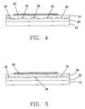
- FIG. 4is a side view of an embodiment of the present invention that includes a substrate, an undercladding layer disposed on the substrate, a core glass layer disposed on a portion of the undercladding layer, and an overcladding layer disposed on the undercladding layer and the core glass layer;
- FIG. 5is a side view of another embodiment of the present invention that includes a substrate, an undercladding layer disposed on the substrate, a core glass layer disposed on a portion of the undercladding layer, a polymer layer disposed on the undercladding layer adjacent the core glass layer, and an overcladding layer disposed on the polymer layer and the core glass layer; and
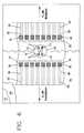
- FIG. 6is a top view of another embodiment of the present invention that includes a substrate, an undercladding layer disposed on the substrate, a core glass layer disposed on a portion of the undercladding layer, a polymer layer disposed on the undercladding layer adjacent the core glass layer, and an overcladding layer disposed on the polymer layer and the core glass layer.
- the present inventionprovides an integrated, high-performance OADM by combining the favorable properties of glass optical waveguides and polymer-based digital optical switches.
- Planar glass technologiesare most suited to the fabrication of AWGs, as they provide low optical loss.
- planar glass technologiesfrequently suffer from polarization dependence caused by the stress of the fabrication process.
- Digital optical switchesare best implemented in polymers because of their large thermo-optic effect and low thermal conductivity.
- low-loss index-matching polymersare used as a top cladding layer for glass-based AWG devices, they can provide benefits such as lowering the overall stress in the device, which reduces the polarization dependence, and lowering the temperature sensitivity of the device, which simplifies temperature control issues.
- the polymer materials for the top cladding applicationwill have a refractive index at the use temperature and wavelength that is 0.5-0.7% less than that of the core glass layer, an optical loss at use wavelengths that is preferably equal to or less than that of the core glass layer (typically 0.1 dB/cm or less), a large (>1 ⁇ 10 ⁇ 4 /° C.), negative thermo-optic coefficient (dn/dT), a low elastic modulus to provide low stress on the silica layers, good adhesion to the glass core and cladding layers, and the ability to be metallized with typical metals used for thermo-optic switches such as chrome and gold. There are a few materials that come close to meeting all of these criteria.
- halofluorinated diacrylatessuch as the chlorofluorodiacrylates developed by AlliedSignal, which include the applications of Wu et al., U.S. application Ser. No. 08/842,783, filed Apr. 17, 1997, entitled “New Photocurable Halofluorinated Acrylates”, and U.S. application Ser. No. 09/190,194 now U.S. Pat. No. 6,166,156, filed Nov. 12, 1998, entitled “New Method for Making Photocurable Halofluorinated Acrylates”, both of which are hereby incorporated by reference.
- These materialshave a refractive index at 1550 nm and 70° C. of approximately 1.44, meeting well the refractive index criteria above.
- optical loss of this polymeris between 0.1 and 0.2 dB/cm at 1550 nm, dn/dT is approximately ⁇ 2 ⁇ 10 ⁇ 4 /° C., and good adhesion to glass and silicon oxide substrates has been achieved.
- FIG. 3A schematic of the invention is shown in FIG. 3 .
- Polymer-based digital optical switches 14are “add/drop” 2 ⁇ 2s, rather than full crossbar 2 ⁇ 2s, since the two states of the switch are the “through” state and the “add/drop” states, respectively.
- a polymer overcladding(shown in FIG. 4 as polymer overcladding 24 ) is applied everywhere in the device and also serves as a segmented core in the switching regions (which are fairly short).
- Fiber arraysshown in FIG. 3 as Add fiber array 16 and Drop fiber array 18 ) are aligned to substrate 10 at the add and drop ports to provide access to detectors and lasers which, in another embodiment, can be integrated as well.
- the integrated OADM of the inventionis a multilayer stack.
- a side view of an embodiment of the inventionis shown in FIG. 4 .
- the integrated OADM illustrated in FIG. 4uses a single polymer approach, wherein the overcladding layer 24 serves as a top cladding and also contains optical switches.
- the first layer of the multilayer stackis a silicon or silica substrate 10 .
- the second layeris an undercladding layer 20 , which can also be a buffer glass layer, formed, for example, by chemical vapor deposition (CVD) or flame hydrolysis.
- the third layeris a glass core layer 22 that can be defined by reactive ion etching (RIE) as part of a semiconductor type fabrication process, and patterned as conventional AWGs.
- RIEreactive ion etching
- Glass core layer 22can also be defined by ion exchange, which does not require the removal of material to make the core.
- the fourth layer of the multilayer stackis an overcladding layer 24 .
- Overcladding layer 24can be formed by spin-coating and subsequent ultraviolet curing/thermal annealing.
- FIG. 4also illustrates a heater 30 , preferably a metal heater, disposed on the overcladding layer 24 . Heater 30 can be patterned using conventional lithographic processes.
- the output of the demultiplexing AWG on the input side of the structureis N waveguides, where N is the number of wavelength channels. These waveguides lead to the switching region.
- the glass coreis segmented to provide gaps into which polymer material is deposited during the subsequent overcladding spin-coating process.
- the gaps in the segmented waveguide regionare designed to provide digital switching action, reasonably low insertion loss, and low return loss.
- this polymerIn the case of the single polymer approach, this polymer must simultaneously be a suitable top cladding material, provide low insertion loss, reduce polarization dependence, and reduce temperature sensitivity. These constraints are removed if two different polymers are used, i.e., a first polymer is used for filling the gaps of the segmented glass core and a second polymer is used as a top cladding.
- FIG. 5A side view of the two polymer approach is shown in FIG. 5 .
- the integrated OADMhas a first polymer, polymer layer 26 , disposed between undercladding layer 20 (and adjacent core glass layer 22 ) and a second polymer, overcladding layer 24 .
- the refractive index of polymer layer 26is adjusted to match the refractive index of glass core layer 22
- the index of overcladding layer 24is adjusted to match the index of undercladding layer 20 .
- Polymer layer 26can be formed by spin-coating and subsequent ultraviolet curing/thermal annealing. Additionally, the polymer layer 26 can be patterned, with direct lithography or reactive ion etching techniques, to further ensure low-loss singlemode operation of the optical switch portion of the OADM.
- the patterning of the polymer layercan proceed via standard photolithographic steps. After the core glass layer has been patterned and the region for the polymer waveguides cleared of core layer glass, the polymer core layer can be spun onto the substrate.
- the polymerwill preferably have an excellent ability to planarize, in which case the height of the polymer layer and the glass core can be made nearly the same.
- the substrate with uncured polymer filmis placed in a nitrogen purged mask aligning compartment. The required photomask is brought into contact with the substrate and adjusted so that good alignment is achieved with the cores of the glass waveguides. UV radiation is then provided, which cures the polymer in the clear regions of the mask (coinciding to the positions of the waveguide cores).
- the maskis removed and the substrate is developed with common organic solvents such as methanol or acetone.
- the top cladding layeris then applied by spin coating over the hybrid polymer/glass structure.
- the core polymer layer indexwill match that of the core glass at the use temperature and wavelength(s).
- RIEreactive ion etching
- a uniform film of polymeris spun and dried, to which is added an evaporated layer of metal (often a titanium/gold combination).
- a photoresistis applied on the metal layer and patterned in a manner similar to the direct photolithographic layer described above.
- the metalis removed with a metal etchant in regions that will be removed by RIE. Finally, RIE is applied to remove the unwanted material and form the polymer waveguide core. Photoresist and metal residues are removed using wet chemical etchants, and the resulting polymer waveguide core is then covered with a top cladding layer as discussed above.
- FIG. 6illustrates a top view of a single polymer approach embodiment of the present invention.
- undercladding layer 20is disposed on substrate 10 .
- Core glass layer 22is disposed on a portion of undercladding layer 20 and polymer layer 26 is disposed on the undercladding layer adjacent the core glass layer.
- the polymer layers 26include an optical switch 14 , shown in FIG. 6 as 1 ⁇ 2 digital optical switches.
- Each of the switches 14may also include a metal heater 30 .
- the inset of FIG. 6illustrates a 2 ⁇ 2 switch 15 composed of four 1 ⁇ 2 switches 14 .
- Overcladding layer 24is disposed on polymer layer 26 and core glass layer 22 .
- the present inventionprovides an integrated, high-performance OADM that is compact in size by virtue of using polymer-based digital optical switches.
- the OADM of the inventionhas the advantages of low power consumption, reduced polarization dependence in the AWG region, reduced thermal sensitivity in the AWG region, reduced stress in the device overall, reduced cost over non-integrated OADMs, lower crosstalk than available from Mach-Zehnder embodiments, ability to readily adopt more flexible and complex switching elements, much lower loss than in a pure polymer embodiment, and lower loss than can be achieved stringing together conventional off-the-shelf components.
Landscapes
- Physics & Mathematics (AREA)
- General Physics & Mathematics (AREA)
- Optics & Photonics (AREA)
- Engineering & Computer Science (AREA)
- Microelectronics & Electronic Packaging (AREA)
- Nonlinear Science (AREA)
- Optical Integrated Circuits (AREA)
Abstract
Description
Claims (33)
Priority Applications (1)
| Application Number | Priority Date | Filing Date | Title |
|---|---|---|---|
| US09/658,469US6385362B1 (en) | 1999-09-08 | 2000-09-08 | Hybrid integrated optical add-drop multiplexer |
Applications Claiming Priority (2)
| Application Number | Priority Date | Filing Date | Title |
|---|---|---|---|
| US15286299P | 1999-09-08 | 1999-09-08 | |
| US09/658,469US6385362B1 (en) | 1999-09-08 | 2000-09-08 | Hybrid integrated optical add-drop multiplexer |
Publications (1)
| Publication Number | Publication Date |
|---|---|
| US6385362B1true US6385362B1 (en) | 2002-05-07 |
Family
ID=22544775
Family Applications (1)
| Application Number | Title | Priority Date | Filing Date |
|---|---|---|---|
| US09/658,469Expired - LifetimeUS6385362B1 (en) | 1999-09-08 | 2000-09-08 | Hybrid integrated optical add-drop multiplexer |
Country Status (8)
| Country | Link |
|---|---|
| US (1) | US6385362B1 (en) |
| EP (1) | EP1218781B1 (en) |
| JP (1) | JP2003508814A (en) |
| CN (2) | CN1267757C (en) |
| AU (1) | AU7355700A (en) |
| CA (1) | CA2384157A1 (en) |
| DE (1) | DE60038121T2 (en) |
| WO (1) | WO2001018573A1 (en) |
Cited By (15)
| Publication number | Priority date | Publication date | Assignee | Title |
|---|---|---|---|---|
| US20030128917A1 (en)* | 2001-07-20 | 2003-07-10 | Turpin Terry M. | Method and apparatus for optical signal processing using an optical tapped delay line |
| US6611638B2 (en)* | 2001-01-16 | 2003-08-26 | Hitachi, Ltd. | High performance optical add/drop multiplexer and optical wavelength multiplexing network |
| US6658179B2 (en)* | 2001-11-08 | 2003-12-02 | Xerox Corporation | Monolithic reconfigurable optical multiplexer systems and methods |
| US20050069248A1 (en)* | 2003-08-11 | 2005-03-31 | Jasti Chandra Sekhar | Method and apparatus for balancing the power of optical channels traversing an optical add drop multiplexer |
| US20050175041A1 (en)* | 2004-02-10 | 2005-08-11 | Hitachi Communication Technologies, Ltd. | Optical add-drop multiplexer |
| US6954561B1 (en)* | 2001-07-16 | 2005-10-11 | Applied Materials Inc | Methods for forming thermo-optic switches, routers and attenuators |
| US20050281295A1 (en)* | 2004-06-16 | 2005-12-22 | Fishman Daniel A | Optical add/drop multiplexer having an alternated channel configuration |
| US20050281557A1 (en)* | 2004-06-16 | 2005-12-22 | Fishman Daniel A | Optical add/drop multiplexer having a banded channel configuration |
| US20080056638A1 (en)* | 2006-08-31 | 2008-03-06 | Glebov Alexei L | Polarization-Independent Electro-Optical (EO) Switching |
| US20080106527A1 (en)* | 2006-11-06 | 2008-05-08 | Rpo Pty Limited | Waveguide Configurations for Minimising Substrate Area |
| US20080107387A1 (en)* | 2006-11-07 | 2008-05-08 | Raszka Scott A | Light conduits having peripheral, shape-defining polymer overmolds |
| US8867874B2 (en)* | 2012-12-06 | 2014-10-21 | Finisar Sweden Ab | Method for modifying the combining or splitting ratio of a multimode interference coupler |
| US11381760B2 (en)* | 2018-12-07 | 2022-07-05 | James Scholtz | Infrared imager and related systems |
| US20220286221A1 (en)* | 2019-09-06 | 2022-09-08 | Telefonaktiebolaget Lm Ericsson (Publ) | Optical Node and Optical Transceiver for Auto Tuning of Operational Wavelength |
| US11638982B2 (en) | 2016-10-21 | 2023-05-02 | Applied Materials, Inc. | Core configuration for in-situ electromagnetic induction monitoring system |
Families Citing this family (6)
| Publication number | Priority date | Publication date | Assignee | Title |
|---|---|---|---|---|
| US7145704B1 (en) | 2003-11-25 | 2006-12-05 | Cheetah Omni, Llc | Optical logic gate based optical router |
| US6888661B1 (en) | 2002-06-13 | 2005-05-03 | Cheetah Omni, Llc | Square filter function tunable optical devices |
| US8285150B2 (en) | 2006-10-02 | 2012-10-09 | Futurewei Technologies, Inc. | Method and system for integrated DWDM transmitters |
| US8285149B2 (en) | 2006-10-02 | 2012-10-09 | Futurewei Technologies, Inc. | Method and system for integrated DWDM transmitters |
| US8050525B2 (en) | 2006-10-11 | 2011-11-01 | Futurewei Technologies, Inc. | Method and system for grating taps for monitoring a DWDM transmitter array integrated on a PLC platform |
| US8285151B2 (en)* | 2006-10-20 | 2012-10-09 | Futurewei Technologies, Inc. | Method and system for hybrid integrated 1XN DWDM transmitter |
Citations (6)
| Publication number | Priority date | Publication date | Assignee | Title |
|---|---|---|---|---|
| US5546483A (en)* | 1993-08-02 | 1996-08-13 | Nippon Telegraph And Telephone Corporation | Integrated optical waveguide circuit and optical branch line test system using the same |
| US5857039A (en)* | 1996-03-20 | 1999-01-05 | France Telecom | Mixed silica/polymer active directional coupler, in integrated optics |
| US5859941A (en) | 1995-12-07 | 1999-01-12 | Kokusai Denshin Denwa Kabushiki Kaisha | Optical add/drop multiplexer device |
| US6084050A (en) | 1997-01-09 | 2000-07-04 | Nippon Telegraph And Telephone Corporation | Thermo-optic devices |
| US6091870A (en) | 1998-02-20 | 2000-07-18 | Corning Incorporated | Wavelength division multiplexer/demultiplexer optical device |
| US6122416A (en)* | 1997-09-26 | 2000-09-19 | Nippon Telegraph And Telephone Corporation | Stacked thermo-optic switch, switch matrix and add-drop multiplexer having the stacked thermo-optic switch |
Family Cites Families (6)
| Publication number | Priority date | Publication date | Assignee | Title |
|---|---|---|---|---|
| JPH04238305A (en)* | 1991-01-22 | 1992-08-26 | Nippon Telegr & Teleph Corp <Ntt> | Polymer coated glass core optical waveguide |
| CA2130605A1 (en)* | 1993-08-24 | 1995-02-25 | Arjen F. Bakker | Polymeric thermo-optic device |
| EP0642052A1 (en)* | 1993-08-24 | 1995-03-08 | Akzo Nobel N.V. | Polymeric thermo-optical waveguide device |
| JPH1068833A (en)* | 1996-08-29 | 1998-03-10 | Nippon Telegr & Teleph Corp <Ntt> | Optical waveguide, method of manufacturing the same, and optical circuit |
| JPH11160741A (en)* | 1997-09-26 | 1999-06-18 | Nippon Telegr & Teleph Corp <Ntt> | Stacked thermo-optic switch, switch matrix and optical add / drop multiplexer including the switch as a component |
| JP3713942B2 (en)* | 1998-02-20 | 2005-11-09 | 日立電線株式会社 | Waveguide type optical switch |
- 2000
- 2000-09-08WOPCT/US2000/024563patent/WO2001018573A1/enactiveIP Right Grant
- 2000-09-08CNCN200410059881.0Apatent/CN1267757C/ennot_activeExpired - Fee Related
- 2000-09-08DEDE60038121Tpatent/DE60038121T2/ennot_activeExpired - Lifetime
- 2000-09-08JPJP2001522110Apatent/JP2003508814A/ennot_activeCeased
- 2000-09-08USUS09/658,469patent/US6385362B1/ennot_activeExpired - Lifetime
- 2000-09-08CACA002384157Apatent/CA2384157A1/ennot_activeAbandoned
- 2000-09-08AUAU73557/00Apatent/AU7355700A/ennot_activeAbandoned
- 2000-09-08EPEP00961635Apatent/EP1218781B1/ennot_activeExpired - Lifetime
- 2000-09-08CNCNB008125546Apatent/CN1176389C/ennot_activeExpired - Fee Related
Patent Citations (6)
| Publication number | Priority date | Publication date | Assignee | Title |
|---|---|---|---|---|
| US5546483A (en)* | 1993-08-02 | 1996-08-13 | Nippon Telegraph And Telephone Corporation | Integrated optical waveguide circuit and optical branch line test system using the same |
| US5859941A (en) | 1995-12-07 | 1999-01-12 | Kokusai Denshin Denwa Kabushiki Kaisha | Optical add/drop multiplexer device |
| US5857039A (en)* | 1996-03-20 | 1999-01-05 | France Telecom | Mixed silica/polymer active directional coupler, in integrated optics |
| US6084050A (en) | 1997-01-09 | 2000-07-04 | Nippon Telegraph And Telephone Corporation | Thermo-optic devices |
| US6122416A (en)* | 1997-09-26 | 2000-09-19 | Nippon Telegraph And Telephone Corporation | Stacked thermo-optic switch, switch matrix and add-drop multiplexer having the stacked thermo-optic switch |
| US6091870A (en) | 1998-02-20 | 2000-07-18 | Corning Incorporated | Wavelength division multiplexer/demultiplexer optical device |
Cited By (26)
| Publication number | Priority date | Publication date | Assignee | Title |
|---|---|---|---|---|
| US6611638B2 (en)* | 2001-01-16 | 2003-08-26 | Hitachi, Ltd. | High performance optical add/drop multiplexer and optical wavelength multiplexing network |
| US6954561B1 (en)* | 2001-07-16 | 2005-10-11 | Applied Materials Inc | Methods for forming thermo-optic switches, routers and attenuators |
| US20030128917A1 (en)* | 2001-07-20 | 2003-07-10 | Turpin Terry M. | Method and apparatus for optical signal processing using an optical tapped delay line |
| US7509048B2 (en) | 2001-07-20 | 2009-03-24 | Essex Corporation | Method and apparatus for optical signal processing using an optical tapped delay line |
| US6990265B2 (en) | 2001-11-08 | 2006-01-24 | Xerox Corporation | Monolithic reconfigurable optical multiplexer systems and methods |
| US6658179B2 (en)* | 2001-11-08 | 2003-12-02 | Xerox Corporation | Monolithic reconfigurable optical multiplexer systems and methods |
| US20040114856A1 (en)* | 2001-11-08 | 2004-06-17 | Xerox Corporation | Monolithic reconfigurable optical multiplexer systems and methods |
| US20050069248A1 (en)* | 2003-08-11 | 2005-03-31 | Jasti Chandra Sekhar | Method and apparatus for balancing the power of optical channels traversing an optical add drop multiplexer |
| US7151875B2 (en) | 2003-08-11 | 2006-12-19 | General Instrument Corporation | Method and apparatus for balancing the power of optical channels traversing an optical add drop multiplexer |
| US7903975B2 (en)* | 2004-02-10 | 2011-03-08 | Hitachi, Ltd. | Optical add-drop multiplexer |
| US20050175041A1 (en)* | 2004-02-10 | 2005-08-11 | Hitachi Communication Technologies, Ltd. | Optical add-drop multiplexer |
| US7286763B2 (en) | 2004-06-16 | 2007-10-23 | Lucent Technologies Inc. | Optical add/drop multiplexer having a banded channel configuration |
| US20050281557A1 (en)* | 2004-06-16 | 2005-12-22 | Fishman Daniel A | Optical add/drop multiplexer having a banded channel configuration |
| US20050281295A1 (en)* | 2004-06-16 | 2005-12-22 | Fishman Daniel A | Optical add/drop multiplexer having an alternated channel configuration |
| US7529442B2 (en) | 2006-08-31 | 2009-05-05 | Fujitsu Limited | Polarization-independent electro-optical (EO) switching |
| US20080056638A1 (en)* | 2006-08-31 | 2008-03-06 | Glebov Alexei L | Polarization-Independent Electro-Optical (EO) Switching |
| US20080106527A1 (en)* | 2006-11-06 | 2008-05-08 | Rpo Pty Limited | Waveguide Configurations for Minimising Substrate Area |
| US20080107387A1 (en)* | 2006-11-07 | 2008-05-08 | Raszka Scott A | Light conduits having peripheral, shape-defining polymer overmolds |
| US7400795B2 (en)* | 2006-11-07 | 2008-07-15 | Schott Corporation | Light conduits having peripheral, shape-defining polymer overmolds |
| US8867874B2 (en)* | 2012-12-06 | 2014-10-21 | Finisar Sweden Ab | Method for modifying the combining or splitting ratio of a multimode interference coupler |
| US11638982B2 (en) | 2016-10-21 | 2023-05-02 | Applied Materials, Inc. | Core configuration for in-situ electromagnetic induction monitoring system |
| US12103135B2 (en) | 2016-10-21 | 2024-10-01 | Applied Materials, Inc. | Core configuration for in-situ electromagnetic induction monitoring system |
| US11381760B2 (en)* | 2018-12-07 | 2022-07-05 | James Scholtz | Infrared imager and related systems |
| US12238449B2 (en) | 2018-12-07 | 2025-02-25 | James I. Scholtz | Infrared imager and related systems |
| US20220286221A1 (en)* | 2019-09-06 | 2022-09-08 | Telefonaktiebolaget Lm Ericsson (Publ) | Optical Node and Optical Transceiver for Auto Tuning of Operational Wavelength |
| US12143202B2 (en)* | 2019-09-06 | 2024-11-12 | Telefonaktiebolaget Lm Ericsson (Publ) | Optical node and optical transceiver for auto tuning of operational wavelength |
Also Published As
| Publication number | Publication date |
|---|---|
| AU7355700A (en) | 2001-04-10 |
| EP1218781A4 (en) | 2006-05-17 |
| CN1267757C (en) | 2006-08-02 |
| JP2003508814A (en) | 2003-03-04 |
| DE60038121T2 (en) | 2009-03-05 |
| CA2384157A1 (en) | 2001-03-15 |
| CN1372647A (en) | 2002-10-02 |
| EP1218781A1 (en) | 2002-07-03 |
| DE60038121D1 (en) | 2008-04-03 |
| EP1218781B1 (en) | 2008-02-20 |
| CN1553239A (en) | 2004-12-08 |
| WO2001018573A1 (en) | 2001-03-15 |
| CN1176389C (en) | 2004-11-17 |
Similar Documents
| Publication | Publication Date | Title |
|---|---|---|
| US6385362B1 (en) | Hybrid integrated optical add-drop multiplexer | |
| US6122416A (en) | Stacked thermo-optic switch, switch matrix and add-drop multiplexer having the stacked thermo-optic switch | |
| Eldada | Polymer integrated optics: promise versus practicality | |
| US6724968B2 (en) | Photodefinition of optical devices | |
| CN113050222B (en) | Reconfigurable polymer mode converter for mode division multiplexing system | |
| US6233378B1 (en) | Optical switch utilizing two unidirectional waveguide couplers | |
| EP1438612B1 (en) | Mechanical beam steering for optical integrated circuits | |
| Clemens et al. | Wavelength-adaptable optical phased array in SiO 2-Si | |
| Goh | Recent advances in large-scale silica-based thermo-optic switches | |
| Eldada et al. | Polymeric components for all-optical networks | |
| Kribich et al. | Thermo-optic switches using sol-gel processed hybrid materials | |
| Eldada | Nanoengineered polymers for photonic integrated circuits | |
| Eldada et al. | Fully reconfigurable optical add/drop multiplexing subsystem on a chip | |
| Yao et al. | Polymeric planar waveguide devices for photonic network applications | |
| JPH10333105A (en) | Polymer optical waveguide tunable filter | |
| Maalouf et al. | Polymer optical circuits technology for large-scale integration of passive functions | |
| JPH11160741A (en) | Stacked thermo-optic switch, switch matrix and optical add / drop multiplexer including the switch as a component | |
| Maruno | Planar Lightwave Circuit (PLC) | |
| Ooba et al. | Planar-waveguide-type optical switching devices | |
| Ticknor et al. | Integrated switches for reconfigurable optical add-drop modules | |
| Hibino | PLC-type Thermooptic Switches | |
| Toyoda et al. | Thermo-optic devices using polymer waveguides | |
| Takahashi et al. | An optical switch using a replicated polymer optical waveguide | |
| Izuhara et al. | Chip-scale fully reconfigurable optical add/drop multiplexing subsystem in polymer microphotonic circuits | |
| Yao | DWDM applications |
Legal Events
| Date | Code | Title | Description |
|---|---|---|---|
| AS | Assignment | Owner name:CORNING INCORPORATED, NEW YORK Free format text:ASSIGNMENT OF ASSIGNORS INTEREST;ASSIGNOR:NORWOOD, ROBERT A.;REEL/FRAME:011316/0004 Effective date:20001121 | |
| STCF | Information on status: patent grant | Free format text:PATENTED CASE | |
| AS | Assignment | Owner name:E. I. DU PONT DE NEMOURS AND COMPANY, DELAWARE Free format text:ASSIGNMENT OF ASSIGNORS INTEREST;ASSIGNOR:CORNING INCORPORATED;REEL/FRAME:013699/0033 Effective date:20030214 | |
| FPAY | Fee payment | Year of fee payment:4 | |
| FEPP | Fee payment procedure | Free format text:PAT HOLDER CLAIMS SMALL ENTITY STATUS, ENTITY STATUS SET TO SMALL (ORIGINAL EVENT CODE: LTOS); ENTITY STATUS OF PATENT OWNER: SMALL ENTITY | |
| AS | Assignment | Owner name:ENABLENCE TECHNOLOGIES USA INC., CANADA Free format text:ASSIGNMENT OF ASSIGNORS INTEREST;ASSIGNOR:E.I. DU PONT DE NEMOURS AND COMPANY;REEL/FRAME:022510/0050 Effective date:20080731 | |
| FPAY | Fee payment | Year of fee payment:8 | |
| FPAY | Fee payment | Year of fee payment:12 |