US6385265B1 - Differential charge pump - Google Patents
Differential charge pumpDownload PDFInfo
- Publication number
- US6385265B1 US6385265B1US09/128,901US12890198AUS6385265B1US 6385265 B1US6385265 B1US 6385265B1US 12890198 AUS12890198 AUS 12890198AUS 6385265 B1US6385265 B1US 6385265B1
- Authority
- US
- United States
- Prior art keywords
- differential
- output
- receive
- signal
- transistor
- Prior art date
- Legal status (The legal status is an assumption and is not a legal conclusion. Google has not performed a legal analysis and makes no representation as to the accuracy of the status listed.)
- Expired - Lifetime
Links
- 239000000872bufferSubstances0.000claimsabstractdescription30
- 238000000034methodMethods0.000claimsabstractdescription12
- 230000000295complement effectEffects0.000claims4
- 238000010586diagramMethods0.000description10
- 230000003068static effectEffects0.000description6
- 230000003139buffering effectEffects0.000description2
- 230000007704transitionEffects0.000description2
- 230000005540biological transmissionEffects0.000description1
- 239000003990capacitorSubstances0.000description1
- 238000011084recoveryMethods0.000description1
- 238000005070samplingMethods0.000description1
- 230000035945sensitivityEffects0.000description1
Images


Classifications
- H—ELECTRICITY
- H03—ELECTRONIC CIRCUITRY
- H03L—AUTOMATIC CONTROL, STARTING, SYNCHRONISATION OR STABILISATION OF GENERATORS OF ELECTRONIC OSCILLATIONS OR PULSES
- H03L7/00—Automatic control of frequency or phase; Synchronisation
- H03L7/06—Automatic control of frequency or phase; Synchronisation using a reference signal applied to a frequency- or phase-locked loop
- H03L7/08—Details of the phase-locked loop
- H03L7/085—Details of the phase-locked loop concerning mainly the frequency- or phase-detection arrangement including the filtering or amplification of its output signal
- H03L7/089—Details of the phase-locked loop concerning mainly the frequency- or phase-detection arrangement including the filtering or amplification of its output signal the phase or frequency detector generating up-down pulses
- H03L7/0891—Details of the phase-locked loop concerning mainly the frequency- or phase-detection arrangement including the filtering or amplification of its output signal the phase or frequency detector generating up-down pulses the up-down pulses controlling source and sink current generators, e.g. a charge pump
- H03L7/0893—Details of the phase-locked loop concerning mainly the frequency- or phase-detection arrangement including the filtering or amplification of its output signal the phase or frequency detector generating up-down pulses the up-down pulses controlling source and sink current generators, e.g. a charge pump the up-down pulses controlling at least two source current generators or at least two sink current generators connected to different points in the loop
- H—ELECTRICITY
- H03—ELECTRONIC CIRCUITRY
- H03L—AUTOMATIC CONTROL, STARTING, SYNCHRONISATION OR STABILISATION OF GENERATORS OF ELECTRONIC OSCILLATIONS OR PULSES
- H03L7/00—Automatic control of frequency or phase; Synchronisation
- H03L7/06—Automatic control of frequency or phase; Synchronisation using a reference signal applied to a frequency- or phase-locked loop
- H03L7/08—Details of the phase-locked loop
- H03L7/085—Details of the phase-locked loop concerning mainly the frequency- or phase-detection arrangement including the filtering or amplification of its output signal
- H03L7/089—Details of the phase-locked loop concerning mainly the frequency- or phase-detection arrangement including the filtering or amplification of its output signal the phase or frequency detector generating up-down pulses
- H03L7/0891—Details of the phase-locked loop concerning mainly the frequency- or phase-detection arrangement including the filtering or amplification of its output signal the phase or frequency detector generating up-down pulses the up-down pulses controlling source and sink current generators, e.g. a charge pump
- H03L7/0895—Details of the current generators
- H03L7/0896—Details of the current generators the current generators being controlled by differential up-down pulses
Definitions
- the present inventionrelates to phase-locked loops (PLLs) generally and, more particularly, to a charge pump that may be used in a PLL.
- PLLsphase-locked loops
- Phase-locked loop (PLL) based clock recovery systemsoften employ charge pumps as internal circuitry.
- a low static phase offset in the PLLleads to longer possible transmission lengths due to the more ideal sampling point of the incoming data.
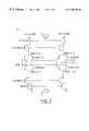
- a circuit 10 illustrating a typical charge pumpis shown.
- the circuit 10receives a signal PUMPUP and PUMPDN, which can be divided into pairs of signals PUMPUPP and PUMPUPN, and PUMPDND and PUMPDNN, respectively.
- the non-filter drain of the current steering differential pairsis tied to a fixed voltage (i.e., VMID) which is most likely different from the other drain of the differential pair (i.e., FILTU and FILTD).
- the sources of the differential pairsmove from one voltage to another, based upon the difference between the signals FILTU and FILTD and the signal VMID.
- the net resultis a mismatch between the signal FILTU_PUMP and the signal FILTD_PUMP.
- the common mode correction circuiti.e., the transistors connected to the signals CM_PBIAS and CM_BIAS
- Another disadvantage with the circuit 10is the lack of cascoded current sources. Due to the low output impedance of a single device, noticeable current variations can occur with changes in the signals FILTU and FILTD. This can also result in static phase offset.
- the use of the signal VMID on the gate of one side of the differential pairreduces the operating frequency of the pump, which becomes significant at lower voltages.
- CM 13 PBIAS and CM_NBIAStwo common mode signals are needed (i.e., CM 13 PBIAS and CM_NBIAS). This increases the complexity of the common mode control circuit.
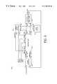
- the circuit 50comprises a voltage source 52 , a voltage source 54 , a switch S 1 , a switch S 2 , a switch S 3 , a switch S 4 and a comparator 56 .
- the circuit 50is a single-ended system, which is more sensitive to voltage supply noise and has a smaller dynamic range of operation when compared with the circuit of FIG. 1 .
- the smaller dynamic range of operationrequires a voltage controlled oscillator (VCO) to have a higher gain, which in turn increases the noise sensitivity.
- VCOvoltage controlled oscillator
- the present inventionconcerns a circuit and method comprising a charge pump having a first and a second differential element.
- the charge pumpmay be configured to generate a first and a second output signal in response to the first and second differential elements.
- the first differential elementmay comprise (i) a first unity gain buffer and (ii) a first and a second transistor pair configured to receive a first and second control signal.
- the second differential elementmay comprise (i) a second unity gain buffer and (ii) a third and a fourth transistor pair configured to receive the first and second control signals.
- the first and second unity gain buffersmay stabilize the source nodes of each of the transistors pairs.
- the objects, features and advantages of the present inventioninclude a charge pump that may be used in a phase-locked loop that may provide (i) reduced static phase offset,(ii) fewer noise sources, (iii) an increased operating frequency that may compensate for lower supply voltages, (iv) lower voltage operation, and (v) may be implemented using a smaller die area.
- FIG. 1is a circuit diagram of a conventional charge pump
- FIG. 2is a circuit diagram of a conventional buffering scheme
- FIG. 3is a block diagram of a preferred embodiment of the present invention.
- FIG. 4is a circuit diagram of an example of the charge pump of FIG. 3;
- FIG. 5is a circuit diagram of an example of the unity gain buffer of FIG. 3.
- FIG. 6is a circuit diagram of an example of the common mode control circuit of FIG. 3 .
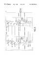
- the circuit 100generally comprises a phase detector block (or circuit) 102 , a common mode control block (or circuit) 104 , a charge pump block (or circuit) 106 , a voltage controlled oscillator (VCO) block (or circuit) 108 and a loop filter block (or circuit) 110 .
- phase detector blockor circuit
- common mode control blockor circuit
- charge pump blockor circuit
- VCOvoltage controlled oscillator
- the phase detector 102generally comprises an input 112 that may receive a data signal (e.g., CLOCK/DATA), an input 114 that may receive a clock signal (e.g., VCO_CLK) from the VCO block 108 , an output 116 that may present a first control signal (e.g., PUMPUP) and an output 118 that may present a second control signal (e.g., PUMPDN).
- the charge pump 106generally comprises an input 120 that may receive the signal PUMPUP, an input 122 that may receive the signal PUMPDN, an output 124 that may present a control signal (e.g., FILTU) and an output 126 that may present a control signal (e.g., FILTD).
- the charge pump 106may also comprise a number of input 128 a - 128 n that may receive a number of bias signals.
- the input 128 amay receive a bias signal (e.g., CM 13 PBIAS) that may be generated by the common mode control block 104 .
- the input 128 bmay receive a bias signal (e.g., PBIAS)
- the input 128 cmay receive a bias signal (e.g., PBIASC)
- the input 128 dmay receive a bias signal (e.g., NBIASC)
- the input 128 nmay receive a bias signal (e.g., NBIAS).
- the common mode control block 104generally comprises an output 130 that may present the signal CM_PBIAS, an input 132 that may receive the signal NBIAS, an input 134 that may receive the signal FILTU and an input 136 that may receive the signal FILTD.
- the voltage controlled oscillator block 106generally comprises an input 138 that may receive the signal FILTU, an input 140 that may receive the signal FILTD and an output 142 that may present the signal VCO_CLK.
- the loop filter block 110generally comprises an input/output 144 that may be connected to the output 124 of the charge pump 106 and an input/output 146 that may be connected to the output 126 of the charge pump 106 .
- the signals NBIAS, PBIAS, NBIASC and PBIASCmay be generated by an external circuit, such as an analog bias circuit.
- the signal CM_PBIASmay be a common mode bias signal that may be presented to the charge pump 106 .
- the loop filter 108may comprise a number of resistors and/or capacitors.
- the charge pump circuit 106generally comprises a first differential element 160 and a second differential element 162 .
- the first differential element 160generally presents the signal FILTU at the output 124
- the second differential element 162generally presents the signal FILTD at the output 126 .
- the first differential element 160generally comprises a transistor 164 a, a transistor 166 a, a transistor 168 a, a transistor 170 a, a transistor 172 a, a transistor 174 a, a transistor 176 a, a transistor 178 a, a transistor 180 a and a unity gain buffer circuit 200 a.
- the transistors 170 a and 180 agenerally form a differential pair 171 a.
- the transistors 172 a and 178 agenerally form a differential pair 173 a.
- the transistors 170 b and 180 bgenerally form a differential pair 171 b.
- the transistors 172 b and 178 bgenerally form a differential pair 173 b.
- the unity gain buffer circuit 200 ahas an input 202 a and an output 204 a and will be described in more detail in connection with FIG. 5 .
- the transistor 164 agenerally comprises a gate that may receive the signal PBIAS.
- the transistor 166 agenerally has a gate that may receive the signal CM_PBIAS.
- the transistor 168 agenerally has a gate that may receive the signal PBIASC.
- the transistor 170 amay have a gate that may receive the signal PUMPUPN.
- the transistor 172 agenerally comprises a gate that may receive the signal PUMPDNP.
- the transistor 174 agenerally comprises a gate that may receive the signal NBIASC.
- the transistor 176 agenerally comprises a gate that may receive the signal NBIAS.
- the transistor 178 agenerally comprises a gate that may receive the signal PUMPDNN.
- the transistor 180 agenerally comprises a gate that may receive the signal PUMPUPP.
- the signal PUMPUPN and PUMPUPPgenerally comprise a differential input that may be presented to the transistors 170 a and 180 a, respectively, of the differential pair 171 a.
- the signals PUMPDNP and PUMPDNNgenerally comprise a differential input that is presented to the transistors 172 a and 178 a, respectively, of the differential pair 173 a.
- the differential element 162generally comprises a transistor 164 b, 166 b, 168 b, 170 b, 172 b, 174 b, 176 b, 178 b, 180 b and a unity gain buffer 200 b.
- the transistors 164 b - 180 b and the unity gain buffer 200 bhave similar connections to the transistors 164 a - 180 a and the unity gain buffer 200 a of the differential element 160 .
- the transistor 170 bgenerally receives the signal PUMPDNN
- the transistor 172 bgenerally receives the signal PUMPUPP
- the transistor 178 bgenerally receives the signal PUMPUPN
- the transistor 180 bgenerally receives the signal PUMPDNP.
- the unity gain buffers 200 a and 200 bgenerally force the drains at both sides of the individual differential transistor pairs (e.g., 173 a or 173 b ) to be equal. This generally minimizes the switching transients on the source nodes of the differential pairs (e.g., the pairs 171 a, 171 b , 173 a and 173 b ) that may be created when the signals PUMPUP and PUMPDN transition from one side to the other. This may lead to a mismatch between the signal FILTU and the signal FILTD, which may result in lower static phase offset.
- the cascoded current sourcesmay increase the output impedance of the current sources (e.g., the transistors 168 a and 168 b ), which may reduce variation in current due to differences in the signals FILTU and FILTD, which may, in turn, reduce the static phase offset.
- the simplified common mode biasingmay result in smaller die area and fewer noise sources.
- Driving the differential pairse.g., the pairs 171 a, 171 b , 173 a and 173 b
- increases the operating frequency of the devicecompensating for performance loss at lower voltage operation (e.g., 3.3V or less).
- the unity gain buffer 200 bmay have similar connections.
- the unity gain buffer 200 agenerally comprises a transistor 210 , a transistor 212 , a transistor 214 , a transistor 216 , a transistor 218 , a transistor 220 , a transistor 222 , a transistor 224 and a transistor 226 .
- the transistors 210 and 212generally receive the signal PBIAS.
- the transistors 214 and 220generally receive the signal PBIASC.
- the transistor 216generally receives the signal FILTU.
- the gate of the transistor 222 as well as the drain of the transistors 220 and 224generally present the signal OUT at the output 204 a.
- the transistor 218is generally connected between the transistor 214 and ground.
- the transistor 224is generally coupled between the transistor 220 and ground.
- the transistor 226is generally coupled between the sources of the transistors 216 and 222 and ground. While the circuit 200 shows one example of a unity gain buffer, other buffers that provide similar functioning (e.g., providing a uniform voltage) may be used accordingly to meet the design criteria of a particular implementation.
- the common mode circuit 104generally comprises a transistor 250 , a transistor 252 , a transistor 254 , a transistor 256 , a transistor 258 , a transistor 260 , a transistor 262 and a transistor 264 .
- the transistor 254may receive the signal FILTU and the transistor 260 may receive the signal FILTD.
- the gates of the transistors 256 and 258may receive the signal CM_VREF.
- the transistors 262 and 264may receive the signal NBIAS.
- the drains of the transistors 256 and 258 as well as the drain and gate of the transistor 252may present the signal CM_PBIAS.
- the transistor 250may be coupled between a supply voltage and the drains of the transistors 254 and 260 .
- the transistor 252may be connected between the supply voltage and the drains of the transistors 256 and 258 .
- the transistors 262 and 264may be connected between ground and the sources of the transistors 254 and 256 and the sources of the transistors 258 and 260 , respectively.
Landscapes
- Stabilization Of Oscillater, Synchronisation, Frequency Synthesizers (AREA)
Abstract
Description
Claims (20)
Priority Applications (1)
| Application Number | Priority Date | Filing Date | Title |
|---|---|---|---|
| US09/128,901US6385265B1 (en) | 1998-08-04 | 1998-08-04 | Differential charge pump |
Applications Claiming Priority (1)
| Application Number | Priority Date | Filing Date | Title |
|---|---|---|---|
| US09/128,901US6385265B1 (en) | 1998-08-04 | 1998-08-04 | Differential charge pump |
Publications (1)
| Publication Number | Publication Date |
|---|---|
| US6385265B1true US6385265B1 (en) | 2002-05-07 |
Family
ID=22437538
Family Applications (1)
| Application Number | Title | Priority Date | Filing Date |
|---|---|---|---|
| US09/128,901Expired - LifetimeUS6385265B1 (en) | 1998-08-04 | 1998-08-04 | Differential charge pump |
Country Status (1)
| Country | Link |
|---|---|
| US (1) | US6385265B1 (en) |
Cited By (37)
| Publication number | Priority date | Publication date | Assignee | Title |
|---|---|---|---|---|
| US6472921B1 (en)* | 2001-05-31 | 2002-10-29 | Siemens Aktiengesellschaft | Delivering a fine delay stage for a delay locked loop |
| US6556067B2 (en)* | 2000-06-13 | 2003-04-29 | Linfinity Microelectronics | Charge pump regulator with load current control |
| US6636104B2 (en) | 2000-06-13 | 2003-10-21 | Microsemi Corporation | Multiple output charge pump |
| US20030223525A1 (en)* | 2002-05-30 | 2003-12-04 | Broadcom Corporation | Method and apparatus for high speed signal recovery |
| US6686794B1 (en)* | 2002-12-19 | 2004-02-03 | Intel Corporation | Differential charge pump |
| US20040101081A1 (en)* | 2002-11-27 | 2004-05-27 | Tse-Hsiang Hsu | Charge pump structure for reducing capacitance in loop filter of a phase locked loop |
| US20040119544A1 (en)* | 2002-12-20 | 2004-06-24 | Lee Jin-Kug | Differential charge pump and phase locked loop having the same |
| US20040135603A1 (en)* | 2003-01-14 | 2004-07-15 | Samsung Electronics Co., Ltd. | Differential charge pump and method therefor, and phase locked loop and method therefor using the pump and method |
| US6812754B1 (en)* | 2000-06-05 | 2004-11-02 | Renesas Technology Corp. | Clock synchronizer with offset prevention function against variation of output potential of loop filter |
| US20050017776A1 (en)* | 2003-06-27 | 2005-01-27 | Keaveney Michael F. | Chopped charge pump |
| US20060044030A1 (en)* | 2004-08-26 | 2006-03-02 | International Business Machines Corporation | Variation tolerant charge leakage correction circuit for phase locked loops |
| WO2006137030A1 (en)* | 2005-06-21 | 2006-12-28 | Nxp B.V. | Phase-locked loop systems using static phase offset calibration |
| US20070164799A1 (en)* | 2006-01-19 | 2007-07-19 | Lattice Semiconductor Corporation | Phase-locked loop systems and methods |
| US20090021310A1 (en)* | 2007-07-16 | 2009-01-22 | Micrel, Inc. | System and method for phase-locked loop (pll) for high-speed memory interface (hsmi) |
| US20090231046A1 (en)* | 2007-02-07 | 2009-09-17 | Little James M | Low spur phase-locked loop architecture |
| US20100066420A1 (en)* | 2008-09-18 | 2010-03-18 | Masaaki Kaneko | Wide Range Operational Charge Pump Circuit |
| US20110193608A1 (en)* | 2010-02-05 | 2011-08-11 | Tyco Healthcare Group Lp | Square Wave For Vessel Sealing |
| US8147489B2 (en) | 2005-01-14 | 2012-04-03 | Covidien Ag | Open vessel sealing instrument |
| US8197633B2 (en) | 2005-09-30 | 2012-06-12 | Covidien Ag | Method for manufacturing an end effector assembly |
| USD680220S1 (en) | 2012-01-12 | 2013-04-16 | Coviden IP | Slider handle for laparoscopic device |
| US8454602B2 (en) | 2009-05-07 | 2013-06-04 | Covidien Lp | Apparatus, system, and method for performing an electrosurgical procedure |
| US8523898B2 (en) | 2009-07-08 | 2013-09-03 | Covidien Lp | Endoscopic electrosurgical jaws with offset knife |
| US8551091B2 (en) | 2002-10-04 | 2013-10-08 | Covidien Ag | Vessel sealing instrument with electrical cutting mechanism |
| US8568444B2 (en) | 2008-10-03 | 2013-10-29 | Covidien Lp | Method of transferring rotational motion in an articulating surgical instrument |
| US8591506B2 (en) | 1998-10-23 | 2013-11-26 | Covidien Ag | Vessel sealing system |
| US8597296B2 (en) | 2003-11-17 | 2013-12-03 | Covidien Ag | Bipolar forceps having monopolar extension |
| US8803572B2 (en)* | 2012-07-12 | 2014-08-12 | Stmicroelectronics International N.V. | Phase locked loop circuit with reduced jitter |
| US8852228B2 (en) | 2009-01-13 | 2014-10-07 | Covidien Lp | Apparatus, system, and method for performing an electrosurgical procedure |
| US8898888B2 (en) | 2009-09-28 | 2014-12-02 | Covidien Lp | System for manufacturing electrosurgical seal plates |
| US9028493B2 (en) | 2009-09-18 | 2015-05-12 | Covidien Lp | In vivo attachable and detachable end effector assembly and laparoscopic surgical instrument and methods therefor |
| US9113940B2 (en) | 2011-01-14 | 2015-08-25 | Covidien Lp | Trigger lockout and kickback mechanism for surgical instruments |
| US9113898B2 (en) | 2008-10-09 | 2015-08-25 | Covidien Lp | Apparatus, system, and method for performing an electrosurgical procedure |
| US10135448B1 (en) | 2017-09-20 | 2018-11-20 | Qualcomm Incorporated | Phase-locked loop (PLL) with charge scaling |
| US10213250B2 (en) | 2015-11-05 | 2019-02-26 | Covidien Lp | Deployment and safety mechanisms for surgical instruments |
| US10251696B2 (en) | 2001-04-06 | 2019-04-09 | Covidien Ag | Vessel sealer and divider with stop members |
| US10277122B1 (en)* | 2018-02-26 | 2019-04-30 | National Chiao Tung University | Charge pump circuit and phase locked loop system using the same |
| US10987159B2 (en) | 2015-08-26 | 2021-04-27 | Covidien Lp | Electrosurgical end effector assemblies and electrosurgical forceps configured to reduce thermal spread |
Citations (19)
| Publication number | Priority date | Publication date | Assignee | Title |
|---|---|---|---|---|
| US4692718A (en) | 1985-04-12 | 1987-09-08 | U.S. Philips Corporation | Tunable astable multivibrator with buffer transistors |
| US4884042A (en) | 1989-02-15 | 1989-11-28 | National Semiconductor Corporation | Dual port voltage controlled emitter coupled multivibrator |
| US5101117A (en) | 1988-02-17 | 1992-03-31 | Mips Computer Systems | Variable delay line phase-locked loop circuit synchronization system |
| US5103191A (en) | 1989-07-25 | 1992-04-07 | Siemens Aktiengesellschaft | Circuit configuration for phase locking |
| US5412349A (en) | 1992-03-31 | 1995-05-02 | Intel Corporation | PLL clock generator integrated with microprocessor |
| US5446867A (en) | 1992-05-29 | 1995-08-29 | Intel Corporation | Microprocessor PLL clock circuit with selectable delayed feedback |
| US5477193A (en)* | 1994-10-21 | 1995-12-19 | Cyrix Corporation | Current source loop filter with automatic gain control |
| US5495207A (en) | 1994-08-31 | 1996-02-27 | International Business Machines Corporation | Differential current controlled oscillator with variable load |
| US5550493A (en) | 1993-09-21 | 1996-08-27 | Ricoh Company Ltd. | Potential comparing circuit having an offset correcting circuit |
| US5619161A (en) | 1994-08-31 | 1997-04-08 | International Business Machines Corporation | Diffrential charge pump with integrated common mode control |
| US5621374A (en) | 1994-12-20 | 1997-04-15 | U.S. Philips Corporation | Amplifying circuit for simulating a unity gain buffer amplifier |
| US5631591A (en) | 1995-05-30 | 1997-05-20 | National Semiconductor Corporation | Method and apparatus for synchronizing timing signals of two integrated circuit chips |
| US5677648A (en)* | 1994-03-24 | 1997-10-14 | Discovision Associates | Noise compensated phase locked loop circuit |
| US5736880A (en) | 1994-12-23 | 1998-04-07 | Sgs-Thomson Microelectronics S.R.L. | Differential charge pump using surtchingly controlled current generators |
| US5736892A (en) | 1993-12-10 | 1998-04-07 | Rambus, Inc. | Differential charge pump circuit with high differential impedance and low common mode impedance |
| US5740213A (en) | 1994-06-03 | 1998-04-14 | Dreyer; Stephen F. | Differential charge pump based phase locked loop or delay locked loop |
| US5828262A (en)* | 1996-09-30 | 1998-10-27 | Cypress Semiconductor Corp. | Ultra low power pumped n-channel output buffer with self-bootstrap |
| US5903195A (en)* | 1998-01-30 | 1999-05-11 | International Business Machines Corporation | Automatically ranging phase locked loop circuit for microprocessor clock generation |
| US6043695A (en)* | 1997-05-29 | 2000-03-28 | Nec Corporation | Phase locked loop using a schmitt trigger block |
- 1998
- 1998-08-04USUS09/128,901patent/US6385265B1/ennot_activeExpired - Lifetime
Patent Citations (19)
| Publication number | Priority date | Publication date | Assignee | Title |
|---|---|---|---|---|
| US4692718A (en) | 1985-04-12 | 1987-09-08 | U.S. Philips Corporation | Tunable astable multivibrator with buffer transistors |
| US5101117A (en) | 1988-02-17 | 1992-03-31 | Mips Computer Systems | Variable delay line phase-locked loop circuit synchronization system |
| US4884042A (en) | 1989-02-15 | 1989-11-28 | National Semiconductor Corporation | Dual port voltage controlled emitter coupled multivibrator |
| US5103191A (en) | 1989-07-25 | 1992-04-07 | Siemens Aktiengesellschaft | Circuit configuration for phase locking |
| US5412349A (en) | 1992-03-31 | 1995-05-02 | Intel Corporation | PLL clock generator integrated with microprocessor |
| US5446867A (en) | 1992-05-29 | 1995-08-29 | Intel Corporation | Microprocessor PLL clock circuit with selectable delayed feedback |
| US5550493A (en) | 1993-09-21 | 1996-08-27 | Ricoh Company Ltd. | Potential comparing circuit having an offset correcting circuit |
| US5736892A (en) | 1993-12-10 | 1998-04-07 | Rambus, Inc. | Differential charge pump circuit with high differential impedance and low common mode impedance |
| US5677648A (en)* | 1994-03-24 | 1997-10-14 | Discovision Associates | Noise compensated phase locked loop circuit |
| US5740213A (en) | 1994-06-03 | 1998-04-14 | Dreyer; Stephen F. | Differential charge pump based phase locked loop or delay locked loop |
| US5495207A (en) | 1994-08-31 | 1996-02-27 | International Business Machines Corporation | Differential current controlled oscillator with variable load |
| US5619161A (en) | 1994-08-31 | 1997-04-08 | International Business Machines Corporation | Diffrential charge pump with integrated common mode control |
| US5477193A (en)* | 1994-10-21 | 1995-12-19 | Cyrix Corporation | Current source loop filter with automatic gain control |
| US5621374A (en) | 1994-12-20 | 1997-04-15 | U.S. Philips Corporation | Amplifying circuit for simulating a unity gain buffer amplifier |
| US5736880A (en) | 1994-12-23 | 1998-04-07 | Sgs-Thomson Microelectronics S.R.L. | Differential charge pump using surtchingly controlled current generators |
| US5631591A (en) | 1995-05-30 | 1997-05-20 | National Semiconductor Corporation | Method and apparatus for synchronizing timing signals of two integrated circuit chips |
| US5828262A (en)* | 1996-09-30 | 1998-10-27 | Cypress Semiconductor Corp. | Ultra low power pumped n-channel output buffer with self-bootstrap |
| US6043695A (en)* | 1997-05-29 | 2000-03-28 | Nec Corporation | Phase locked loop using a schmitt trigger block |
| US5903195A (en)* | 1998-01-30 | 1999-05-11 | International Business Machines Corporation | Automatically ranging phase locked loop circuit for microprocessor clock generation |
Non-Patent Citations (2)
| Title |
|---|
| Johnson et al., A variable Delay Line PLL for CPU-Coprocessor Synchronization, Oct. 1988, pp. 333-338. |
| Young et al., A PLL Clock Generator with 5 to 110 MHz of Lock Range for Microprocessors, Nov. 1992, pp. 1599-1607. |
Cited By (72)
| Publication number | Priority date | Publication date | Assignee | Title |
|---|---|---|---|---|
| US9375270B2 (en) | 1998-10-23 | 2016-06-28 | Covidien Ag | Vessel sealing system |
| US9375271B2 (en) | 1998-10-23 | 2016-06-28 | Covidien Ag | Vessel sealing system |
| US9463067B2 (en) | 1998-10-23 | 2016-10-11 | Covidien Ag | Vessel sealing system |
| US8591506B2 (en) | 1998-10-23 | 2013-11-26 | Covidien Ag | Vessel sealing system |
| US6812754B1 (en)* | 2000-06-05 | 2004-11-02 | Renesas Technology Corp. | Clock synchronizer with offset prevention function against variation of output potential of loop filter |
| US6812776B2 (en) | 2000-06-13 | 2004-11-02 | Microsemi Corporation | Multiple output charge pump |
| US6897709B2 (en) | 2000-06-13 | 2005-05-24 | Microsemi Corporation | Charge pump regulator with load current control |
| US6556067B2 (en)* | 2000-06-13 | 2003-04-29 | Linfinity Microelectronics | Charge pump regulator with load current control |
| US20030169097A1 (en)* | 2000-06-13 | 2003-09-11 | Henry George C. | Charge pump regulator with load current control |
| US20040080361A1 (en)* | 2000-06-13 | 2004-04-29 | Henry George C. | Multiple output charge pump |
| US6636104B2 (en) | 2000-06-13 | 2003-10-21 | Microsemi Corporation | Multiple output charge pump |
| US10687887B2 (en) | 2001-04-06 | 2020-06-23 | Covidien Ag | Vessel sealer and divider |
| US10251696B2 (en) | 2001-04-06 | 2019-04-09 | Covidien Ag | Vessel sealer and divider with stop members |
| US10265121B2 (en) | 2001-04-06 | 2019-04-23 | Covidien Ag | Vessel sealer and divider |
| US6472921B1 (en)* | 2001-05-31 | 2002-10-29 | Siemens Aktiengesellschaft | Delivering a fine delay stage for a delay locked loop |
| US20030223525A1 (en)* | 2002-05-30 | 2003-12-04 | Broadcom Corporation | Method and apparatus for high speed signal recovery |
| US7386085B2 (en)* | 2002-05-30 | 2008-06-10 | Broadcom Corporation | Method and apparatus for high speed signal recovery |
| US8551091B2 (en) | 2002-10-04 | 2013-10-08 | Covidien Ag | Vessel sealing instrument with electrical cutting mechanism |
| US20040101081A1 (en)* | 2002-11-27 | 2004-05-27 | Tse-Hsiang Hsu | Charge pump structure for reducing capacitance in loop filter of a phase locked loop |
| US7161436B2 (en)* | 2002-11-27 | 2007-01-09 | Mediatek Inc. | Charge pump structure for reducing capacitance in loop filter of a phase locked loop |
| US6686794B1 (en)* | 2002-12-19 | 2004-02-03 | Intel Corporation | Differential charge pump |
| US20040119544A1 (en)* | 2002-12-20 | 2004-06-24 | Lee Jin-Kug | Differential charge pump and phase locked loop having the same |
| US7042261B2 (en)* | 2002-12-20 | 2006-05-09 | Samsung Electronics Co., Ltd. | Differential charge pump and phase locked loop having the same |
| US6900677B2 (en) | 2003-01-14 | 2005-05-31 | Samsung Electronics Co., Ltd. | Differential charge pump and method therefor, and phase locked loop and method therefor using the pump and method |
| US20040135603A1 (en)* | 2003-01-14 | 2004-07-15 | Samsung Electronics Co., Ltd. | Differential charge pump and method therefor, and phase locked loop and method therefor using the pump and method |
| US7202717B2 (en)* | 2003-06-27 | 2007-04-10 | Analog Devices, Inc. | Chopped charge pump |
| WO2005004315A3 (en)* | 2003-06-27 | 2005-10-06 | Analog Devices Inc | Chopped charge pump |
| US20050017776A1 (en)* | 2003-06-27 | 2005-01-27 | Keaveney Michael F. | Chopped charge pump |
| US8597296B2 (en) | 2003-11-17 | 2013-12-03 | Covidien Ag | Bipolar forceps having monopolar extension |
| US10441350B2 (en) | 2003-11-17 | 2019-10-15 | Covidien Ag | Bipolar forceps having monopolar extension |
| US7176731B2 (en)* | 2004-08-26 | 2007-02-13 | International Business Machines Corporation | Variation tolerant charge leakage correction circuit for phase locked loops |
| US20060044030A1 (en)* | 2004-08-26 | 2006-03-02 | International Business Machines Corporation | Variation tolerant charge leakage correction circuit for phase locked loops |
| US8147489B2 (en) | 2005-01-14 | 2012-04-03 | Covidien Ag | Open vessel sealing instrument |
| WO2006137030A1 (en)* | 2005-06-21 | 2006-12-28 | Nxp B.V. | Phase-locked loop systems using static phase offset calibration |
| US8197633B2 (en) | 2005-09-30 | 2012-06-12 | Covidien Ag | Method for manufacturing an end effector assembly |
| US7439783B2 (en)* | 2006-01-19 | 2008-10-21 | Lattice Semiconductor Corporation | Phase-locked loop systems and methods |
| US20070164799A1 (en)* | 2006-01-19 | 2007-07-19 | Lattice Semiconductor Corporation | Phase-locked loop systems and methods |
| US7936223B2 (en)* | 2007-02-07 | 2011-05-03 | Vintomie Networks B.V., Llc | Low spur phase-locked loop architecture |
| US20090231046A1 (en)* | 2007-02-07 | 2009-09-17 | Little James M | Low spur phase-locked loop architecture |
| US7659783B2 (en)* | 2007-07-16 | 2010-02-09 | Micrel, Inc. | System and method for phase-locked loop (PLL) for high-speed memory interface (HSMI) |
| US20090021310A1 (en)* | 2007-07-16 | 2009-01-22 | Micrel, Inc. | System and method for phase-locked loop (pll) for high-speed memory interface (hsmi) |
| US7768326B2 (en)* | 2008-09-18 | 2010-08-03 | Kabushiki Kaisha Toshiba | Wide range operational charge pump circuit |
| US20100066420A1 (en)* | 2008-09-18 | 2010-03-18 | Masaaki Kaneko | Wide Range Operational Charge Pump Circuit |
| US8568444B2 (en) | 2008-10-03 | 2013-10-29 | Covidien Lp | Method of transferring rotational motion in an articulating surgical instrument |
| US9113898B2 (en) | 2008-10-09 | 2015-08-25 | Covidien Lp | Apparatus, system, and method for performing an electrosurgical procedure |
| US9655674B2 (en) | 2009-01-13 | 2017-05-23 | Covidien Lp | Apparatus, system and method for performing an electrosurgical procedure |
| US8852228B2 (en) | 2009-01-13 | 2014-10-07 | Covidien Lp | Apparatus, system, and method for performing an electrosurgical procedure |
| US10085794B2 (en) | 2009-05-07 | 2018-10-02 | Covidien Lp | Apparatus, system and method for performing an electrosurgical procedure |
| US9345535B2 (en) | 2009-05-07 | 2016-05-24 | Covidien Lp | Apparatus, system and method for performing an electrosurgical procedure |
| US8454602B2 (en) | 2009-05-07 | 2013-06-04 | Covidien Lp | Apparatus, system, and method for performing an electrosurgical procedure |
| US8858554B2 (en) | 2009-05-07 | 2014-10-14 | Covidien Lp | Apparatus, system, and method for performing an electrosurgical procedure |
| US9364247B2 (en) | 2009-07-08 | 2016-06-14 | Covidien Lp | Endoscopic electrosurgical jaws with offset knife |
| US8523898B2 (en) | 2009-07-08 | 2013-09-03 | Covidien Lp | Endoscopic electrosurgical jaws with offset knife |
| US9931131B2 (en) | 2009-09-18 | 2018-04-03 | Covidien Lp | In vivo attachable and detachable end effector assembly and laparoscopic surgical instrument and methods therefor |
| US9028493B2 (en) | 2009-09-18 | 2015-05-12 | Covidien Lp | In vivo attachable and detachable end effector assembly and laparoscopic surgical instrument and methods therefor |
| US9750561B2 (en) | 2009-09-28 | 2017-09-05 | Covidien Lp | System for manufacturing electrosurgical seal plates |
| US9265552B2 (en) | 2009-09-28 | 2016-02-23 | Covidien Lp | Method of manufacturing electrosurgical seal plates |
| US11490955B2 (en) | 2009-09-28 | 2022-11-08 | Covidien Lp | Electrosurgical seal plates |
| US11026741B2 (en) | 2009-09-28 | 2021-06-08 | Covidien Lp | Electrosurgical seal plates |
| US8898888B2 (en) | 2009-09-28 | 2014-12-02 | Covidien Lp | System for manufacturing electrosurgical seal plates |
| US10188454B2 (en) | 2009-09-28 | 2019-01-29 | Covidien Lp | System for manufacturing electrosurgical seal plates |
| US20110193608A1 (en)* | 2010-02-05 | 2011-08-11 | Tyco Healthcare Group Lp | Square Wave For Vessel Sealing |
| US9585709B2 (en)* | 2010-02-05 | 2017-03-07 | Covidien Lp | Square wave for vessel sealing |
| US11660108B2 (en) | 2011-01-14 | 2023-05-30 | Covidien Lp | Trigger lockout and kickback mechanism for surgical instruments |
| US9113940B2 (en) | 2011-01-14 | 2015-08-25 | Covidien Lp | Trigger lockout and kickback mechanism for surgical instruments |
| US10383649B2 (en) | 2011-01-14 | 2019-08-20 | Covidien Lp | Trigger lockout and kickback mechanism for surgical instruments |
| USD680220S1 (en) | 2012-01-12 | 2013-04-16 | Coviden IP | Slider handle for laparoscopic device |
| US8803572B2 (en)* | 2012-07-12 | 2014-08-12 | Stmicroelectronics International N.V. | Phase locked loop circuit with reduced jitter |
| US10987159B2 (en) | 2015-08-26 | 2021-04-27 | Covidien Lp | Electrosurgical end effector assemblies and electrosurgical forceps configured to reduce thermal spread |
| US10213250B2 (en) | 2015-11-05 | 2019-02-26 | Covidien Lp | Deployment and safety mechanisms for surgical instruments |
| US10135448B1 (en) | 2017-09-20 | 2018-11-20 | Qualcomm Incorporated | Phase-locked loop (PLL) with charge scaling |
| US10277122B1 (en)* | 2018-02-26 | 2019-04-30 | National Chiao Tung University | Charge pump circuit and phase locked loop system using the same |
Similar Documents
| Publication | Publication Date | Title |
|---|---|---|
| US6385265B1 (en) | Differential charge pump | |
| US6320435B1 (en) | PLL circuit which can reduce phase offset without increase in operation voltage | |
| US6172571B1 (en) | Method for reducing static phase offset in a PLL | |
| US6326852B1 (en) | Low offset and low glitch energy charge pump for PLL-based timing recovery systems | |
| KR100393317B1 (en) | Delayed synchronization loop | |
| JP5110815B2 (en) | Voltage controlled oscillator with stable gain over a wide frequency range | |
| US5298870A (en) | Voltage controlled ring oscillator having differential amplifier stages | |
| US20080284529A1 (en) | Method and apparatus of a ring oscillator for phase locked loop (pll) | |
| JP3109560B2 (en) | Semiconductor integrated circuit using variation compensation technology | |
| US6184732B1 (en) | Setting the common mode level of a differential charge pump output | |
| US20010030572A1 (en) | Differential charge pump with low voltage common mode feedback circuit | |
| JP4160503B2 (en) | Differential ring oscillator stage | |
| US6724230B2 (en) | Semiconductor integrated circuit | |
| US6472914B2 (en) | Process independent ultralow charge pump | |
| US5523723A (en) | Low noise low voltage phase lock loop | |
| US6316927B1 (en) | Voltage output driver and filter | |
| US5714912A (en) | VCO supply voltage regulator | |
| US5880579A (en) | VCO supply voltage regulator for PLL | |
| EP0771491B1 (en) | Very low noise, wide frequency range phase lock loop | |
| US7439783B2 (en) | Phase-locked loop systems and methods | |
| US6831492B1 (en) | Common-bias and differential structure based DLL | |
| JP2755181B2 (en) | Voltage controlled oscillator | |
| US7372341B2 (en) | Noise immunity circuitry for phase locked loops and delay locked loops | |
| US20040119513A1 (en) | Charge pump architecture | |
| JPH09223965A (en) | Clock generation circuit |
Legal Events
| Date | Code | Title | Description |
|---|---|---|---|
| AS | Assignment | Owner name:CYPRESS SEMICONDUCTOR CORPORATION, CALIFORNIA Free format text:ASSIGNMENT OF ASSIGNORS INTEREST;ASSIGNORS:DUFFY, MICHAEL L.;WILLIAMS, BERTRAND J.;KRUCZKOWSKI, PHILLIP J.;AND OTHERS;REEL/FRAME:009364/0475 Effective date:19980804 | |
| STCF | Information on status: patent grant | Free format text:PATENTED CASE | |
| FPAY | Fee payment | Year of fee payment:4 | |
| REMI | Maintenance fee reminder mailed | ||
| FPAY | Fee payment | Year of fee payment:8 | |
| SULP | Surcharge for late payment | Year of fee payment:7 | |
| REMI | Maintenance fee reminder mailed | ||
| FPAY | Fee payment | Year of fee payment:12 | |
| SULP | Surcharge for late payment | Year of fee payment:11 | |
| AS | Assignment | Owner name:MORGAN STANLEY SENIOR FUNDING, INC., NEW YORK Free format text:SECURITY INTEREST;ASSIGNORS:CYPRESS SEMICONDUCTOR CORPORATION;SPANSION LLC;REEL/FRAME:035240/0429 Effective date:20150312 | |
| AS | Assignment | Owner name:CYPRESS SEMICONDUCTOR CORPORATION, CALIFORNIA Free format text:PARTIAL RELEASE OF SECURITY INTEREST IN PATENTS;ASSIGNOR:MORGAN STANLEY SENIOR FUNDING, INC., AS COLLATERAL AGENT;REEL/FRAME:039708/0001 Effective date:20160811 Owner name:SPANSION LLC, CALIFORNIA Free format text:PARTIAL RELEASE OF SECURITY INTEREST IN PATENTS;ASSIGNOR:MORGAN STANLEY SENIOR FUNDING, INC., AS COLLATERAL AGENT;REEL/FRAME:039708/0001 Effective date:20160811 | |
| AS | Assignment | Owner name:MONTEREY RESEARCH, LLC, CALIFORNIA Free format text:ASSIGNMENT OF ASSIGNORS INTEREST;ASSIGNOR:CYPRESS SEMICONDUCTOR CORPORATION;REEL/FRAME:040911/0238 Effective date:20160811 | |
| AS | Assignment | Owner name:MORGAN STANLEY SENIOR FUNDING, INC., NEW YORK Free format text:CORRECTIVE ASSIGNMENT TO CORRECT THE 8647899 PREVIOUSLY RECORDED ON REEL 035240 FRAME 0429. ASSIGNOR(S) HEREBY CONFIRMS THE SECURITY INTERST;ASSIGNORS:CYPRESS SEMICONDUCTOR CORPORATION;SPANSION LLC;REEL/FRAME:058002/0470 Effective date:20150312 |