US6383597B1 - Magnetic recording media with magnetic bit regions patterned by ion irradiation - Google Patents
Magnetic recording media with magnetic bit regions patterned by ion irradiationDownload PDFInfo
- Publication number
- US6383597B1 US6383597B1US09/602,581US60258100AUS6383597B1US 6383597 B1US6383597 B1US 6383597B1US 60258100 AUS60258100 AUS 60258100AUS 6383597 B1US6383597 B1US 6383597B1
- Authority
- US
- United States
- Prior art keywords
- magnetic
- regions
- chemically
- fept
- ordered
- Prior art date
- Legal status (The legal status is an assumption and is not a legal conclusion. Google has not performed a legal analysis and makes no representation as to the accuracy of the status listed.)
- Expired - Lifetime
Links
Images


Classifications
- G—PHYSICS
- G11—INFORMATION STORAGE
- G11B—INFORMATION STORAGE BASED ON RELATIVE MOVEMENT BETWEEN RECORD CARRIER AND TRANSDUCER
- G11B5/00—Recording by magnetisation or demagnetisation of a record carrier; Reproducing by magnetic means; Record carriers therefor
- G11B5/84—Processes or apparatus specially adapted for manufacturing record carriers
- B—PERFORMING OPERATIONS; TRANSPORTING
- B82—NANOTECHNOLOGY
- B82Y—SPECIFIC USES OR APPLICATIONS OF NANOSTRUCTURES; MEASUREMENT OR ANALYSIS OF NANOSTRUCTURES; MANUFACTURE OR TREATMENT OF NANOSTRUCTURES
- B82Y10/00—Nanotechnology for information processing, storage or transmission, e.g. quantum computing or single electron logic
- G—PHYSICS
- G11—INFORMATION STORAGE
- G11B—INFORMATION STORAGE BASED ON RELATIVE MOVEMENT BETWEEN RECORD CARRIER AND TRANSDUCER
- G11B5/00—Recording by magnetisation or demagnetisation of a record carrier; Reproducing by magnetic means; Record carriers therefor
- G11B5/62—Record carriers characterised by the selection of the material
- G11B5/64—Record carriers characterised by the selection of the material comprising only the magnetic material without bonding agent
- G11B5/65—Record carriers characterised by the selection of the material comprising only the magnetic material without bonding agent characterised by its composition
- G11B5/653—Record carriers characterised by the selection of the material comprising only the magnetic material without bonding agent characterised by its composition containing Fe or Ni
- G—PHYSICS
- G11—INFORMATION STORAGE
- G11B—INFORMATION STORAGE BASED ON RELATIVE MOVEMENT BETWEEN RECORD CARRIER AND TRANSDUCER
- G11B5/00—Recording by magnetisation or demagnetisation of a record carrier; Reproducing by magnetic means; Record carriers therefor
- G11B5/62—Record carriers characterised by the selection of the material
- G11B5/64—Record carriers characterised by the selection of the material comprising only the magnetic material without bonding agent
- G11B5/65—Record carriers characterised by the selection of the material comprising only the magnetic material without bonding agent characterised by its composition
- G11B5/656—Record carriers characterised by the selection of the material comprising only the magnetic material without bonding agent characterised by its composition containing Co
- G—PHYSICS
- G11—INFORMATION STORAGE
- G11B—INFORMATION STORAGE BASED ON RELATIVE MOVEMENT BETWEEN RECORD CARRIER AND TRANSDUCER
- G11B5/00—Recording by magnetisation or demagnetisation of a record carrier; Reproducing by magnetic means; Record carriers therefor
- G11B5/74—Record carriers characterised by the form, e.g. sheet shaped to wrap around a drum
- G11B5/743—Patterned record carriers, wherein the magnetic recording layer is patterned into magnetic isolated data islands, e.g. discrete tracks
- G—PHYSICS
- G11—INFORMATION STORAGE
- G11B—INFORMATION STORAGE BASED ON RELATIVE MOVEMENT BETWEEN RECORD CARRIER AND TRANSDUCER
- G11B5/00—Recording by magnetisation or demagnetisation of a record carrier; Reproducing by magnetic means; Record carriers therefor
- G11B5/74—Record carriers characterised by the form, e.g. sheet shaped to wrap around a drum
- G11B5/82—Disk carriers
- G—PHYSICS
- G11—INFORMATION STORAGE
- G11B—INFORMATION STORAGE BASED ON RELATIVE MOVEMENT BETWEEN RECORD CARRIER AND TRANSDUCER
- G11B5/00—Recording by magnetisation or demagnetisation of a record carrier; Reproducing by magnetic means; Record carriers therefor
- G11B5/84—Processes or apparatus specially adapted for manufacturing record carriers
- G11B5/855—Coating only part of a support with a magnetic layer
- G—PHYSICS
- G11—INFORMATION STORAGE
- G11B—INFORMATION STORAGE BASED ON RELATIVE MOVEMENT BETWEEN RECORD CARRIER AND TRANSDUCER
- G11B5/00—Recording by magnetisation or demagnetisation of a record carrier; Reproducing by magnetic means; Record carriers therefor
- G11B2005/0002—Special dispositions or recording techniques
- G11B2005/0026—Pulse recording
- G11B2005/0029—Pulse recording using magnetisation components of the recording layer disposed mainly perpendicularly to the record carrier surface
- G—PHYSICS
- G11—INFORMATION STORAGE
- G11B—INFORMATION STORAGE BASED ON RELATIVE MOVEMENT BETWEEN RECORD CARRIER AND TRANSDUCER
- G11B2220/00—Record carriers by type
- G11B2220/20—Disc-shaped record carriers
- G11B2220/25—Disc-shaped record carriers characterised in that the disc is based on a specific recording technology
- G11B2220/2508—Magnetic discs
- Y—GENERAL TAGGING OF NEW TECHNOLOGICAL DEVELOPMENTS; GENERAL TAGGING OF CROSS-SECTIONAL TECHNOLOGIES SPANNING OVER SEVERAL SECTIONS OF THE IPC; TECHNICAL SUBJECTS COVERED BY FORMER USPC CROSS-REFERENCE ART COLLECTIONS [XRACs] AND DIGESTS
- Y10—TECHNICAL SUBJECTS COVERED BY FORMER USPC
- Y10T—TECHNICAL SUBJECTS COVERED BY FORMER US CLASSIFICATION
- Y10T428/00—Stock material or miscellaneous articles
- Y10T428/12—All metal or with adjacent metals
- Y10T428/12493—Composite; i.e., plural, adjacent, spatially distinct metal components [e.g., layers, joint, etc.]
- Y10T428/12771—Transition metal-base component
- Y10T428/12861—Group VIII or IB metal-base component
- Y10T428/12875—Platinum group metal-base component
- Y—GENERAL TAGGING OF NEW TECHNOLOGICAL DEVELOPMENTS; GENERAL TAGGING OF CROSS-SECTIONAL TECHNOLOGIES SPANNING OVER SEVERAL SECTIONS OF THE IPC; TECHNICAL SUBJECTS COVERED BY FORMER USPC CROSS-REFERENCE ART COLLECTIONS [XRACs] AND DIGESTS
- Y10—TECHNICAL SUBJECTS COVERED BY FORMER USPC
- Y10T—TECHNICAL SUBJECTS COVERED BY FORMER US CLASSIFICATION
- Y10T428/00—Stock material or miscellaneous articles
- Y10T428/24—Structurally defined web or sheet [e.g., overall dimension, etc.]
- Y10T428/24479—Structurally defined web or sheet [e.g., overall dimension, etc.] including variation in thickness
- Y—GENERAL TAGGING OF NEW TECHNOLOGICAL DEVELOPMENTS; GENERAL TAGGING OF CROSS-SECTIONAL TECHNOLOGIES SPANNING OVER SEVERAL SECTIONS OF THE IPC; TECHNICAL SUBJECTS COVERED BY FORMER USPC CROSS-REFERENCE ART COLLECTIONS [XRACs] AND DIGESTS
- Y10—TECHNICAL SUBJECTS COVERED BY FORMER USPC
- Y10T—TECHNICAL SUBJECTS COVERED BY FORMER US CLASSIFICATION
- Y10T428/00—Stock material or miscellaneous articles
- Y10T428/31—Surface property or characteristic of web, sheet or block
Definitions
- This inventionrelates generally to magnetic recording media, and more particularly to patterned magnetic recording disks with discrete magnetic regions or islands.
- HCPhexagonal-close-packed
- CoPtcobalt-platinum
- patterned mediaWith patterned media, the continuous granular magnetic film that covers the disk substrate is replaced by an array of spatially separated discrete magnetic regions or islands, each of which serves as a single magnetic bit.
- the primary approach for producing patterned mediahas been to selectively deposit or remove magnetic material from a magnetic layer on the substrate so that magnetic regions are isolated from one another and surrounded by areas of nonmagnetic material.
- the substrateis covered with a lithographically patterned resist material and a magnetic film is deposited to cover both the areas of resist and the areas of exposed substrate. The resist is dissolved to lift off the magnetic film that covers it, leaving an array of isolated magnetic regions.
- An alternative techniqueis to first deposit a magnetic film on the substrate and then pattern resist material on the magnetic film itself. Magnetic material from the areas not protected by the resist can then be selectively removed by well-known processes. Examples of patterned magnetic media made with these types of lithographic processes are described in U.S. Pat. Nos. 5,587,223; 5,768,075 and 5,820,769.
- an undesirable aspect of the process for patterning media that requires the deposition or removal of materialis that it requires potentially disruptive processing with the magnetic media in place.
- Processes required for the effective removal of resists and for the reliable lift-off of fine metal features over large areascan damage the material left behind and therefore lower production yields.
- these processesmust leave a surface that is clean enough so that the magnetic read/write head supported on the air-bearing slider of the disk drive can fly over the disk surface at very low flying heights, typically below 30 nanometers (nm).
- the ionsmix the Co and Pt atoms at the layer interfaces and substantially reduce the perpendicular magnetocrystalline anisotropy of the film, with the result that the regions of the disk that are not irradiated retain their perpendicular magnetic properties and serve as the magnetic bits.
- Chemically-ordered alloys of FePt and CoPt formed as thin filmshave also been proposed for horizontal magnetic recording media.
- Chemically-ordered alloys of FePt and CoPt, in their bulk form,are known as tetragonal L 1 0 -ordered phase materials (also called CuAu materials). They are known for their high magnetocrystalline anisotropy and magnetic moment, properties that are also desirable for high-density magnetic recording media.
- the c-axis of the L 1 0 phaseis similar to the c-axis of HCP CoPt alloys in that both are the easy axis of magnetization.
- An ion-irradiated patterned diskthat uses a continuous magnetic film of a chemically-ordered Co (or Fe) and Pt (or Pd) alloy with a tetragonal crystalline structure is described in IBM's pending application Ser. No. 09/350,803 filed Jul. 9, 1999.
- the ionscause disordering in the film and produce regions in the film that are low coercivity or magnetically “soft” and have no magnetocrystalline anisotropy, so that the regions of the disk that are not irradiated retain their horizontal magnetic properties and serve as the magnetic bits.
- a patterned magnetic recording diskthat has discrete magnetic regions separated by completely nonmagnetic regions so that only the magnetic regions contribute to the read signal, and that is made by a patterning technique where the mask pattern of holes matches the pattern of discrete magnetic regions of the disk that serve as the magnetic bits.
- the present inventionis a magnetic recording disk wherein the magnetic recording layer is patterned into discrete magnetic and nonmagnetic regions having substantially the same chemical composition, but wherein the nonmagnetic regions have a chemically-ordered L 1 2 crystalline structure and the magnetic regions having a chemically-disordered crystalline structure.
- the inventionis based on the discovery that the chemically-ordered intermetallic compound FePt 3 , which is nonferromagnetic, can be rendered ferromagnetic by ion irradiation. With a clear transformation from nonferromagnetic to ferromagnetic, this FePt 3 material can be patterned by irradiating local regions through a mask to create magnetic regions that serve as the magnetic bits.
- the ionspass through the openings in the mask and impact the chemically-ordered FePt 3 in selected regions corresponding to the pattern of holes in the mask.
- the ionsdisrupt the ordering of the Fe and Pt atoms in the unit cell and transform the FePt 3 into magnetic regions corresponding to the mask pattern, with the regions of the film not impacted by the ions retaining their chemically-ordered structure.
- the coercivity of the magnetic regions in the patterned mediacan be increased by slightly altering the 3:1 ratio of Pt to Fe by increasing the amount of Fe or by adding a third element, such as small amounts of cobalt (Co) and/or nickel (Ni), during the sputter deposition of the FePt 3 film.
- FIG. 1Ais a schematic drawing of the unit cells of the chemically-ordered L 1 2 (or AuCu 3 ) structure of FePt 3 .
- FIG. 1Bis a schematic drawing of the unit cells of the disordered face centered cubic (fcc) structure of FePt 3 .
- FIG. 2is an X-ray diffraction (XRD) scan of the ordered FePt 3 sample before irradiation and after irradiation with N+ ions.
- XRDX-ray diffraction
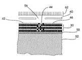
- FIG. 3is a schematic illustration of a discrete chemically-disordered magnetic FePt 3 region separated by chemically-ordered nonmagnetic FePt 3 regions, the magnetic region being formed by ion irradiation through a non-contact stencil mask.
- FIG. 4is a scan with a magneto-optical Kerr looper system across a chemically-ordered FePt 3 sample that was patterned with N+ ions.
- the intermetallic compounds XPt 3such as FePt 3 , form an L 1 2 structure (also known as the AuCu 3 structure) in the chemically-ordered phase and a randomly substituted face-centered-cubic (fcc) structure in the chemically disordered phase, as shown in FIGS. 1A-1B.
- L 1 2 structurealso known as the AuCu 3 structure
- fccface-centered-cubic
- FIGS. 1A-1Bthe chemically-ordered phase
- the corners of the unit cellare occupied with metallic X atoms and the face centers are occupied with the larger Pt atoms.
- each Fe corner atomis shared by 8 neighboring cell corners and each Pt face centered atom is shared by only 2 neighboring cell faces, so that the 1:3 ratio of Fe to Pt is maintained.
- the corner and face center positionsare generally randomly occupied with Pt or X atoms, with the same ratio of Pt to X atoms of 3:1.
- the magnetic properties of FePt 3vary dramatically depending on whether the compound is chemically ordered or disordered. It is known that the chemically-ordered L 1 2 phase of FePt 3 is paramagnetic (no remanent magnetic moment) at room temperature and that this phase is antiferromagnetic (AF) at low temperature.
- the present inventionis based on the discovery that the chemically-disordered phase of FePt 3 created by ion irradiation of the chemically-ordered phase is ferromagnetic with a magnetic moment-per-atom for Fe of 2 Bohr magnetron ( ⁇ B ).
- Ordered FePt 3 alloy filmswere grown epitaxially on MgO (110) and (100) substrates and textured on SiN coated Si wafers.
- the FePt 3 filmswere grown by co-sputtering of Fe and Pt in a 1:3 ratio.
- the substrateswere mounted on a substrate plate heated to 750° C. during deposition, although the substrate itself is somewhat cooler.
- Evidence for the existence of the chemically-ordered structureis found from X-ray diffraction (XRD) and inferred from magnetic measurements.
- XRDX-ray diffraction
- the ordered L 1 2 phasehas tetragonal point symmetry and thus the out-of-plane XRD spectrum shows that (110) and (330) peaks are present.
- the ordered FePt 3 filmsdid not display any room-temperature ferromagnetism, as measured by either SQUID magnetometry or Kerr effect measurements.
- FePt 3 /Co bilayerswere grown to determine if the FePt 3 had the expected AF property. When cooled below 170° K., the bilayer structure was exchange-biased, as would be expected for an AF/ferromagnetic structure like FePt 3 /Co.
- FIG. 2shows the XRD scan of the ordered FePt 3 sample before irradiation and after irradiation with N+ ions at 700 keV at a dose of 2 ⁇ 10 16 ions/cm 2 .
- the ordered FePt 3 (110) peakis reduced by two orders of magnitude and the (330) peak is reduced to background.
- the ordered phaseis reduced to less than 1% of the original volume. Even though the chemical order of the Fe and Pt is disrupted, the crystallographic order is maintained.
- Magnetic hysteresis loop measurementswere made on the irradiated FePt 3 samples at room temperature and 40° K. In-plane magnetic remanence was observed, indicating the disordering caused by the ion irradiation has rendered the films ferromagnetic.
- this FePt 3 materialis well suited for patterning by irradiating local regions to create magnetic regions to serve as the magnetic bits.
- a stencil maskis irradiated with nitrogen ions (N+) at 700 keV and the ions are selectively transmitted through the mask.
- the ionspass through the openings in the mask and impact the ordered FePt 3 in selected regions corresponding to the pattern of holes in the mask.
- the ionsdisrupt the ordering of the Fe and Pt atoms in the unit cell and transform the FePt 3 into magnetic regions corresponding to the mask pattern, with the regions of the film not impacted by the ions retaining their ordered structure.
- FIG. 3illustrates the process schematically, wherein magnetic 44 and nonmagnetic 42 , 46 regions of the film 30 .
- the FePt 3 film 30is formed on a SiN seed layer 50 on silicon substrate 52 .
- the film 30remains chemically-ordered in the L 1 2 phase and thus nonferromagnetic in the regions 42 , 46 that are not aligned with a hole in the silicon stencil mask 60 .
- disorderinghas occurred, and region 44 is now ferromagnetic.
- the irradiated ionshave disrupted the L 1 2 chemical ordering so that the crystalline structure is now fcc, with the Fe and Pt atoms randomly distributed at the corners and face centers of the fcc unit cell. (See FIGS. 1 A- 1 B).
- the film 30 after patterninghas the same chemical composition (FePt 3 ) in both the magnetic and nonmagnetic regions, with the only structural difference in the two types of regions being the crystallographic unit cells.
- the stencil mask 60is a non-contact mask that comprises a wafer, such as silicon, with holes etched through it.
- the ionsdepicted by arrows 62 , are transmitted through the holes in the wafer.
- the silicon stencil maskwas fabricated from a commercial silicon-on-insulator (SOI) wafer with a 10 ⁇ m-thick top side silicon layer, 0.5 ⁇ m of SOI oxide, and a 500 ⁇ m thick silicon carrier substrate.
- SOIsilicon-on-insulator
- the stencil holeswere first patterned by optical lithography and then transferred into the 10 ⁇ m-thick Si layer by SF 6 -based, high aspect ratio reactive ion etching (RIE) with the SOI oxide serving as a reliable etch stop.
- RIEreactive ion etching
- the resulting silicon membraneis approximately 10 ⁇ m thick and covers an area of 1 ⁇ 1 mm.
- the holes in the membraneare nominally 1 ⁇ m in diameter, although somewhat irregular in shape, and are replicated throughout its area with a regular spacing of 1 to 10 ⁇ m.
- two such stencil maskscan be aligned with their holes overlapping to create holes with effective diameters in the range of 100 nm.
- the maskhas holes formed in a pattern to form a magnetic recording disk with concentric circular tracks, with each track having discrete magnetic regions spaced along it to serve as the individually recordable magnetic bits.
- a dose of at least 5 ⁇ 10 15 ions/cm 2 of N+ ions at 700 keVis sufficient to convert the FePt 3 to the chemically-disordered ferromagnetic phase.
- nitrogen ionswere used, other ion species that may be used include ions of He, Ar, Ne, Kr and Xe.
- the voltage and dosage of the ion irradiation required to achieve the desired disruption of the chemically-ordered FePt 3can be determined experimentally.
- FIG. 4The ferromagnetic property of the ion-irradiated region is shown by FIG. 4, where a region of a textured FePt 3 film on SiN has been ion-irradiated. The sample was then scanned using a Kerr magnetometer. Away from the irradiated area, the signal level is in the background of the instrument and then increases in the region irradiated.
- the preferred method for patterning the media with ion irradiationis by a non-contact mask, such as the silicon stencil mask described above.
- a non-contact masksuch as the silicon stencil mask described above.
- the 3:1 ratio of Pt to Fecan be slightly altered by increasing the amount of Fe or by adding a third element, such as small amounts of cobalt (Co) and/or nickel (Ni), during the sputter deposition of the FePt 3 film.
- a third elementsuch as small amounts of cobalt (Co) and/or nickel (Ni)
- Cocobalt
- Ninickel
- phase diagramsit is known from phase diagrams that a Fe(30 to 15 atomic %)-Pt(55 to 85 atomic %) film has a L 1 2 crystalline structure.
- such a slightly modified FePt 3 filmwould still have a substantially L 1 2 chemical ordering and would be nonmagnetic before ion-irradiation.
- palladium (Pd)for a small portion of the Pt, provided the L 1 2 chemically-ordered phase is maintained and provided the desired ferromagnetic properties of the chemically-disordered phase are obtained upon ion irradiation.
Landscapes
- Engineering & Computer Science (AREA)
- Chemical & Material Sciences (AREA)
- Nanotechnology (AREA)
- Physics & Mathematics (AREA)
- Mathematical Physics (AREA)
- Theoretical Computer Science (AREA)
- Crystallography & Structural Chemistry (AREA)
- Magnetic Record Carriers (AREA)
- Manufacturing Of Magnetic Record Carriers (AREA)
Abstract
Description
Claims (7)
Priority Applications (2)
| Application Number | Priority Date | Filing Date | Title |
|---|---|---|---|
| US09/602,581US6383597B1 (en) | 2000-06-21 | 2000-06-21 | Magnetic recording media with magnetic bit regions patterned by ion irradiation |
| KR10-2001-0034451AKR100470772B1 (en) | 2000-06-21 | 2001-06-18 | Magnetic recording media with magnetic bit regions rendered by ion irradiation |
Applications Claiming Priority (1)
| Application Number | Priority Date | Filing Date | Title |
|---|---|---|---|
| US09/602,581US6383597B1 (en) | 2000-06-21 | 2000-06-21 | Magnetic recording media with magnetic bit regions patterned by ion irradiation |
Publications (1)
| Publication Number | Publication Date |
|---|---|
| US6383597B1true US6383597B1 (en) | 2002-05-07 |
Family
ID=24411929
Family Applications (1)
| Application Number | Title | Priority Date | Filing Date |
|---|---|---|---|
| US09/602,581Expired - LifetimeUS6383597B1 (en) | 2000-06-21 | 2000-06-21 | Magnetic recording media with magnetic bit regions patterned by ion irradiation |
Country Status (2)
| Country | Link |
|---|---|
| US (1) | US6383597B1 (en) |
| KR (1) | KR100470772B1 (en) |
Cited By (35)
| Publication number | Priority date | Publication date | Assignee | Title |
|---|---|---|---|---|
| US20020142192A1 (en)* | 2001-03-30 | 2002-10-03 | Kabushiki Kaisha Toshiba | Method of patterning magnetic products using chemical reactions |
| US20030113524A1 (en)* | 2001-10-22 | 2003-06-19 | Klemmer Timothy John | Magnetic films having magnetic and non-magnetic regions and method of producing such films by ion irradiation |
| US20030235717A1 (en)* | 2002-06-21 | 2003-12-25 | Seagate Technology Llc | Multilayer magnetic recording media including composite layer with discontinuous magnetic phase and continuous non-magnetic phase |
| US20040001367A1 (en)* | 2002-06-28 | 2004-01-01 | Seagate Technology Llc | Increased packing density in self-organized magnetic tray |
| US20040080847A1 (en)* | 2002-10-29 | 2004-04-29 | Imation Corp. | Perpendicular patterned magnetic media |
| US20040264026A1 (en)* | 2003-06-25 | 2004-12-30 | Imation Corp. | Encoding techniques for patterned magnetic media |
| US6865044B1 (en) | 2003-12-03 | 2005-03-08 | Hitachi Global Storage Technologies Netherlands B.V. | Method for magnetic recording on patterned multilevel perpendicular media using thermal assistance and fixed write current |
| US20050079647A1 (en)* | 2003-10-08 | 2005-04-14 | International Business Machines Corporation | Method and system for patterning of magnetic thin films using gaseous transformation |
| US6882488B1 (en) | 2003-12-03 | 2005-04-19 | Hitachi Global Storage Technologies Netherlands B.V. | Method for magnetic recording on patterned multilevel perpendicular media using variable write current |
| US6906879B1 (en) | 2003-12-03 | 2005-06-14 | Hitachi Global Storage Technologies Netherlands B.V. | Magnetic recording system with patterned multilevel perpendicular magnetic recording |
| US20050135010A1 (en)* | 2003-12-23 | 2005-06-23 | Seagate Technology Llc | Heat assisted magnetic recording film including superparamagnetic nanoparticles dispersed in an antiferromagnetic or ferrimagnetic matrix |
| US20050170212A1 (en)* | 2004-01-29 | 2005-08-04 | International Business Machines Corporation | Enhancement of magnetic media recording performance using ion irradiation to tailor exchange coupling |
| US6947235B2 (en) | 2003-12-03 | 2005-09-20 | Hitachi Global Storage Technologies Netherlands B.V. | Patterned multilevel perpendicular magnetic recording media |
| US20070042229A1 (en)* | 2005-08-22 | 2007-02-22 | Manfred Albrecht | Longitudinal patterned media with circumferential anisotropy for ultra-high density magnetic recording |
| US20070166839A1 (en)* | 2006-01-18 | 2007-07-19 | Chih-Huang Lai | Method for fabricating magnetoresistance multi-layer |
| US20080075978A1 (en)* | 2006-09-25 | 2008-03-27 | Seagate Technology Llc | CoPtCr-based bit patterned magnetic media |
| US20080102320A1 (en)* | 2004-04-15 | 2008-05-01 | Edelstein Alan S | Non-erasable magnetic identification media |
| US20080112079A1 (en)* | 2006-11-10 | 2008-05-15 | Hitachi Global Storage Technologies Netherlands B.V. | Perpendicular magnetic recording system with patterned medium and manufacturing process for the medium |
| US20080274381A1 (en)* | 2007-05-01 | 2008-11-06 | Hitachi Global Storage Technologies Netherlands B.V. | Perpendicular magnetic recording medium with patterned magnetic islands and nonmagnetic trenches and manufacturing method for suppressing surface diffusion of trench material |
| US20090161254A1 (en)* | 2007-12-21 | 2009-06-25 | Fujitsu Limited | Magnetic recording medium, production method thereof and magnetic disc apparatus |
| US20090201722A1 (en)* | 2008-02-12 | 2009-08-13 | Kamesh Giridhar | Method including magnetic domain patterning using plasma ion implantation for mram fabrication |
| US20090199768A1 (en)* | 2008-02-12 | 2009-08-13 | Steven Verhaverbeke | Magnetic domain patterning using plasma ion implantation |
| US20090273861A1 (en)* | 2008-04-30 | 2009-11-05 | Fujitsu Limited | Manufacturing method of magnetic recording medium, the magnetic recording medium, and magnetic recording and reproducing apparatus |
| US20100098873A1 (en)* | 2008-10-22 | 2010-04-22 | Applied Materials, Inc. | Patterning of magnetic thin film using energized ions |
| US20100096256A1 (en)* | 2008-02-12 | 2010-04-22 | Omkaram Nalamasu | Patterning of magnetic thin film using energized ions and thermal excitation |
| US20100221581A1 (en)* | 2006-10-20 | 2010-09-02 | Lee Kim Y | Process for fabricating patterned magnetic recording media |
| US20100258431A1 (en)* | 2009-04-10 | 2010-10-14 | Applied Materials, Inc. | Use special ion source apparatus and implant with molecular ions to process hdd (high density magnetic disks) with patterned magnetic domains |
| US20100270710A1 (en)* | 2007-12-21 | 2010-10-28 | Industry-Academic Cooperation Foundation Yonsei University | Forming method of magnetic pattern and manufacturing method of patterned media using the same |
| US20100277829A1 (en)* | 2007-12-26 | 2010-11-04 | Showa Denko K.K. | Method for producing magnetic recording medium, and magnetic recording/reproducing apparatus |
| DE202010010593U1 (en)* | 2010-07-23 | 2011-10-24 | Different Power Ideas Gmbh | Machine for converting electrical and / or magnetic energy into mechanical energy or for converting mechanical energy into electrical energy |
| US20140036388A1 (en)* | 2012-03-16 | 2014-02-06 | University College London | System and method for manipulating domain pinning and reversal in ferromagnetic materials |
| US20140218824A1 (en)* | 2013-02-06 | 2014-08-07 | HGST Netherlands B.V. | Reduced adjacent track errors in bit-patterned media |
| US9030780B2 (en) | 2012-08-08 | 2015-05-12 | The United States Of America As Represented By The Secretary Of The Army | Method and apparatus for reading a non-volatile memory using a spin torque oscillator |
| US20150243303A1 (en)* | 2006-04-06 | 2015-08-27 | Sigma Pro Ltd. Llc | Magnetic Storage Medium Comprised of Magnetic Nanoparticles Contained Within Nanotubes |
| US9245617B2 (en) | 2013-12-17 | 2016-01-26 | The United States Of America As Represented By The Secretary Of The Army | Nonvolatile memory cells programable by phase change and method |
Citations (4)
| Publication number | Priority date | Publication date | Assignee | Title |
|---|---|---|---|---|
| US4093453A (en)* | 1974-12-20 | 1978-06-06 | Sony Corporation | Method of making an ordered alloy |
| US5587223A (en) | 1992-10-19 | 1996-12-24 | Board Of Trustees Leland Stanford, Jr. University | High density magnetic information storage medium |
| US5768075A (en) | 1991-12-17 | 1998-06-16 | Baradun R&D Ltd. | Disk medium w/magnetically filled features aligned in rows and columns |
| US5820769A (en) | 1995-05-24 | 1998-10-13 | Regents Of The University Of Minnesota | Method for making magnetic storage having discrete elements with quantized magnetic moments |
Family Cites Families (3)
| Publication number | Priority date | Publication date | Assignee | Title |
|---|---|---|---|---|
| US4992901A (en)* | 1990-02-15 | 1991-02-12 | Seagate Technology, Inc. | Self aligned magnetic poles using sacrificial mask |
| US6331364B1 (en)* | 1999-07-09 | 2001-12-18 | International Business Machines Corporation | Patterned magnetic recording media containing chemically-ordered FePt of CoPt |
| US6440520B1 (en)* | 1999-07-09 | 2002-08-27 | International Business Machines Corporation | Patterned magnetic recording disk with substrate patterned by ion implantation |
- 2000
- 2000-06-21USUS09/602,581patent/US6383597B1/ennot_activeExpired - Lifetime
- 2001
- 2001-06-18KRKR10-2001-0034451Apatent/KR100470772B1/ennot_activeExpired - Fee Related
Patent Citations (4)
| Publication number | Priority date | Publication date | Assignee | Title |
|---|---|---|---|---|
| US4093453A (en)* | 1974-12-20 | 1978-06-06 | Sony Corporation | Method of making an ordered alloy |
| US5768075A (en) | 1991-12-17 | 1998-06-16 | Baradun R&D Ltd. | Disk medium w/magnetically filled features aligned in rows and columns |
| US5587223A (en) | 1992-10-19 | 1996-12-24 | Board Of Trustees Leland Stanford, Jr. University | High density magnetic information storage medium |
| US5820769A (en) | 1995-05-24 | 1998-10-13 | Regents Of The University Of Minnesota | Method for making magnetic storage having discrete elements with quantized magnetic moments |
Non-Patent Citations (7)
| Title |
|---|
| B. D. Terris, et al., "Ion-Beam Patterning of Magnetic Films Using Stencil Masks," Applied Physics Letters, vol. 75, No. 3, Jul. 19, 1999, pp. 403-405. |
| Bruenger, W., Torkler, M., Dzionk, C., Terris, B., Folks, L., Weller, D., Rothuizen, H., Vettiger, P., Stangl, G., Fallmann, W., Micro., Eng., 53, 2000, 605.** |
| C. Chappert, et al., "Planar Patterned Magnetic Media Obtained by Ion Irradiation," www.sciencemag.org-Science, vol. 280, Jun. 19, 1998, pp. 1919-1922. |
| C. Chappert, et al., "Planar Patterned Magnetic Media Obtained by Ion Irradiation," www.sciencemag.org—Science, vol. 280, Jun. 19, 1998, pp. 1919-1922. |
| Le Floc'h, D., Saha-Dasgupta, T., Finel, A., Comp. Mat. Sci., 8, 1997, 192.** |
| Li, N., Bruce, L., Oh-Hun, K., J. Magn. Magn. Mat., 205, 1999, 1.** |
| Oppeneer P., Antonov, V., Kraft, T., Eschrig, H., Yaresko, A., and Perlov, A., J. Phys. Cond., Mat., 8, 1996, 5769.** |
Cited By (66)
| Publication number | Priority date | Publication date | Assignee | Title |
|---|---|---|---|---|
| US6841224B2 (en)* | 2001-03-30 | 2005-01-11 | Kabushiki Kaisha Toshiba | Method of patterning magnetic products using chemical reactions |
| US20020142192A1 (en)* | 2001-03-30 | 2002-10-03 | Kabushiki Kaisha Toshiba | Method of patterning magnetic products using chemical reactions |
| US7232621B2 (en) | 2001-03-30 | 2007-06-19 | Kabushiki Kaisha Toshiba | Method of patterning magnetic products using chemical reaction |
| US7166261B2 (en)* | 2001-03-30 | 2007-01-23 | Kabushiki Kaisha Toshiba | Method of patterning products using chemical reaction |
| US20040191557A1 (en)* | 2001-03-30 | 2004-09-30 | Kabushiki Kaisha Toshiba | Method of patterning magnetic products using chemical reaction |
| US20040258833A1 (en)* | 2001-03-30 | 2004-12-23 | Kabushiki Kaisha Toshiba | Method of patterning magnetic products using chemical reaction |
| US20030113524A1 (en)* | 2001-10-22 | 2003-06-19 | Klemmer Timothy John | Magnetic films having magnetic and non-magnetic regions and method of producing such films by ion irradiation |
| US6849349B2 (en) | 2001-10-22 | 2005-02-01 | Carnegie Mellon University | Magnetic films having magnetic and non-magnetic regions and method of producing such films by ion irradiation |
| US7128987B2 (en) | 2002-06-21 | 2006-10-31 | Seagate Technology Llc | Multilayer magnetic recording media including composite layer with discontinuous magnetic phase and continuous non-magnetic phase |
| US20030235717A1 (en)* | 2002-06-21 | 2003-12-25 | Seagate Technology Llc | Multilayer magnetic recording media including composite layer with discontinuous magnetic phase and continuous non-magnetic phase |
| US6838195B2 (en) | 2002-06-28 | 2005-01-04 | Seagate Technology Llc | Increased packing density in self-organized magnetic tray |
| US20040001367A1 (en)* | 2002-06-28 | 2004-01-01 | Seagate Technology Llc | Increased packing density in self-organized magnetic tray |
| US6999279B2 (en) | 2002-10-29 | 2006-02-14 | Imation Corp. | Perpendicular patterned magnetic media |
| US20040080847A1 (en)* | 2002-10-29 | 2004-04-29 | Imation Corp. | Perpendicular patterned magnetic media |
| US20040264026A1 (en)* | 2003-06-25 | 2004-12-30 | Imation Corp. | Encoding techniques for patterned magnetic media |
| US7050251B2 (en) | 2003-06-25 | 2006-05-23 | Imation Corp. | Encoding techniques for patterned magnetic media |
| US20050079647A1 (en)* | 2003-10-08 | 2005-04-14 | International Business Machines Corporation | Method and system for patterning of magnetic thin films using gaseous transformation |
| US7611911B2 (en) | 2003-10-08 | 2009-11-03 | International Business Machines Corporation | Method and system for patterning of magnetic thin films using gaseous transformation to transform a magnetic portion to a non-magnetic portion |
| US6947235B2 (en) | 2003-12-03 | 2005-09-20 | Hitachi Global Storage Technologies Netherlands B.V. | Patterned multilevel perpendicular magnetic recording media |
| US6906879B1 (en) | 2003-12-03 | 2005-06-14 | Hitachi Global Storage Technologies Netherlands B.V. | Magnetic recording system with patterned multilevel perpendicular magnetic recording |
| US6882488B1 (en) | 2003-12-03 | 2005-04-19 | Hitachi Global Storage Technologies Netherlands B.V. | Method for magnetic recording on patterned multilevel perpendicular media using variable write current |
| US6865044B1 (en) | 2003-12-03 | 2005-03-08 | Hitachi Global Storage Technologies Netherlands B.V. | Method for magnetic recording on patterned multilevel perpendicular media using thermal assistance and fixed write current |
| CN1306480C (en)* | 2003-12-03 | 2007-03-21 | 日立环球储存科技荷兰有限公司 | Magnetic recording system with patterned multilevel perpendicular magnetic recording |
| US20050135010A1 (en)* | 2003-12-23 | 2005-06-23 | Seagate Technology Llc | Heat assisted magnetic recording film including superparamagnetic nanoparticles dispersed in an antiferromagnetic or ferrimagnetic matrix |
| US7158346B2 (en) | 2003-12-23 | 2007-01-02 | Seagate Technology Llc | Heat assisted magnetic recording film including superparamagnetic nanoparticles dispersed in an antiferromagnetic or ferrimagnetic matrix |
| US7425353B2 (en)* | 2004-01-29 | 2008-09-16 | International Business Machines Corporation | Enhancement of magnetic media recording performance using ion irradiation to tailor exchange coupling |
| US20050170212A1 (en)* | 2004-01-29 | 2005-08-04 | International Business Machines Corporation | Enhancement of magnetic media recording performance using ion irradiation to tailor exchange coupling |
| US20080292906A1 (en)* | 2004-01-29 | 2008-11-27 | International Business Machines Corporation | Enhancement of Magnetic Media Recording Performance Using Ion Irradiation to Tailor Exchange Coupling |
| US20080102320A1 (en)* | 2004-04-15 | 2008-05-01 | Edelstein Alan S | Non-erasable magnetic identification media |
| US20070042229A1 (en)* | 2005-08-22 | 2007-02-22 | Manfred Albrecht | Longitudinal patterned media with circumferential anisotropy for ultra-high density magnetic recording |
| US7713591B2 (en)* | 2005-08-22 | 2010-05-11 | Hitachi Global Storage Technologies Netherlands B.V. | Longitudinal patterned media with circumferential anisotropy for ultra-high density magnetic recording |
| US20070166839A1 (en)* | 2006-01-18 | 2007-07-19 | Chih-Huang Lai | Method for fabricating magnetoresistance multi-layer |
| US20150243303A1 (en)* | 2006-04-06 | 2015-08-27 | Sigma Pro Ltd. Llc | Magnetic Storage Medium Comprised of Magnetic Nanoparticles Contained Within Nanotubes |
| US9633676B2 (en)* | 2006-04-06 | 2017-04-25 | Gula Consulting Limited Liability Company | Magnetic storage medium comprised of magnetic nanoparticles contained within nanotubes |
| US8673466B2 (en) | 2006-09-25 | 2014-03-18 | Seagate Technology Llc | CoPtCr-based bit patterned magnetic media |
| US20080075978A1 (en)* | 2006-09-25 | 2008-03-27 | Seagate Technology Llc | CoPtCr-based bit patterned magnetic media |
| US8460565B2 (en) | 2006-10-20 | 2013-06-11 | Seagate Technology Llc | Process for fabricating patterned magnetic recording device |
| US20100221581A1 (en)* | 2006-10-20 | 2010-09-02 | Lee Kim Y | Process for fabricating patterned magnetic recording media |
| US20080112079A1 (en)* | 2006-11-10 | 2008-05-15 | Hitachi Global Storage Technologies Netherlands B.V. | Perpendicular magnetic recording system with patterned medium and manufacturing process for the medium |
| US7732071B2 (en) | 2006-11-10 | 2010-06-08 | Hitachi Global Storage Technologies Netherlands B.V. | Perpendicular magnetic recording system with patterned medium and manufacturing process for the medium |
| US20080274381A1 (en)* | 2007-05-01 | 2008-11-06 | Hitachi Global Storage Technologies Netherlands B.V. | Perpendicular magnetic recording medium with patterned magnetic islands and nonmagnetic trenches and manufacturing method for suppressing surface diffusion of trench material |
| US7846565B2 (en) | 2007-05-01 | 2010-12-07 | Hitachi Golbal Storage Technologies Netherlands B.V. | Perpendicular magnetic recording disk drive with patterned disk having capping layer for suppression of surface diffusion of trench material |
| US20100110581A1 (en)* | 2007-05-01 | 2010-05-06 | Hitachi Global Storage Technologies Netherlands B.V. | Perpendicular magnetic recording disk drive with patterned disk having capping layer for suppression of surface diffusion of trench material |
| US7670696B2 (en) | 2007-05-01 | 2010-03-02 | Hitachi Global Storage Technologies Netherlands B.V. | Perpendicular magnetic recording medium with patterned magnetic islands and nonmagnetic trenches and manufacturing method for suppressing surface diffusion of trench material |
| US20090161254A1 (en)* | 2007-12-21 | 2009-06-25 | Fujitsu Limited | Magnetic recording medium, production method thereof and magnetic disc apparatus |
| US7927725B2 (en)* | 2007-12-21 | 2011-04-19 | Showa Denko K.K. | Magnetic recording medium, production method thereof and magnetic disc apparatus |
| US20100270710A1 (en)* | 2007-12-21 | 2010-10-28 | Industry-Academic Cooperation Foundation Yonsei University | Forming method of magnetic pattern and manufacturing method of patterned media using the same |
| US20100277829A1 (en)* | 2007-12-26 | 2010-11-04 | Showa Denko K.K. | Method for producing magnetic recording medium, and magnetic recording/reproducing apparatus |
| US8551349B2 (en)* | 2007-12-26 | 2013-10-08 | Showa Denko K.K. | Method for producing magnetic recording medium, and magnetic recording/reproducing apparatus |
| US20090199768A1 (en)* | 2008-02-12 | 2009-08-13 | Steven Verhaverbeke | Magnetic domain patterning using plasma ion implantation |
| US9263078B2 (en) | 2008-02-12 | 2016-02-16 | Applied Materials, Inc. | Patterning of magnetic thin film using energized ions |
| US20090201722A1 (en)* | 2008-02-12 | 2009-08-13 | Kamesh Giridhar | Method including magnetic domain patterning using plasma ion implantation for mram fabrication |
| US20100096256A1 (en)* | 2008-02-12 | 2010-04-22 | Omkaram Nalamasu | Patterning of magnetic thin film using energized ions and thermal excitation |
| US8551578B2 (en)* | 2008-02-12 | 2013-10-08 | Applied Materials, Inc. | Patterning of magnetic thin film using energized ions and thermal excitation |
| US8067104B2 (en)* | 2008-04-30 | 2011-11-29 | Fujitsu Limited | Manufacturing method of magnetic recording medium, the magnetic recording medium, and magnetic recording and reproducing apparatus |
| US20090273861A1 (en)* | 2008-04-30 | 2009-11-05 | Fujitsu Limited | Manufacturing method of magnetic recording medium, the magnetic recording medium, and magnetic recording and reproducing apparatus |
| US8535766B2 (en) | 2008-10-22 | 2013-09-17 | Applied Materials, Inc. | Patterning of magnetic thin film using energized ions |
| US20100098873A1 (en)* | 2008-10-22 | 2010-04-22 | Applied Materials, Inc. | Patterning of magnetic thin film using energized ions |
| US20100258431A1 (en)* | 2009-04-10 | 2010-10-14 | Applied Materials, Inc. | Use special ion source apparatus and implant with molecular ions to process hdd (high density magnetic disks) with patterned magnetic domains |
| DE202010010593U1 (en)* | 2010-07-23 | 2011-10-24 | Different Power Ideas Gmbh | Machine for converting electrical and / or magnetic energy into mechanical energy or for converting mechanical energy into electrical energy |
| US20140036388A1 (en)* | 2012-03-16 | 2014-02-06 | University College London | System and method for manipulating domain pinning and reversal in ferromagnetic materials |
| US9030780B2 (en) | 2012-08-08 | 2015-05-12 | The United States Of America As Represented By The Secretary Of The Army | Method and apparatus for reading a non-volatile memory using a spin torque oscillator |
| US9047881B2 (en) | 2012-08-08 | 2015-06-02 | The United States Of America As Represented By The Secretary Of The Army | Nonvolatile corruption resistent magnetic memory and method thereof |
| US20140218824A1 (en)* | 2013-02-06 | 2014-08-07 | HGST Netherlands B.V. | Reduced adjacent track errors in bit-patterned media |
| US9190093B2 (en)* | 2013-02-06 | 2015-11-17 | HGST Netherlands, B.V. | Reduced adjacent track errors in bit-patterned media |
| US9245617B2 (en) | 2013-12-17 | 2016-01-26 | The United States Of America As Represented By The Secretary Of The Army | Nonvolatile memory cells programable by phase change and method |
Also Published As
| Publication number | Publication date |
|---|---|
| KR100470772B1 (en) | 2005-03-08 |
| KR20010114151A (en) | 2001-12-29 |
Similar Documents
| Publication | Publication Date | Title |
|---|---|---|
| US6383597B1 (en) | Magnetic recording media with magnetic bit regions patterned by ion irradiation | |
| US6331364B1 (en) | Patterned magnetic recording media containing chemically-ordered FePt of CoPt | |
| US6391430B1 (en) | Patterned magnetic recording media with discrete magnetic regions separated by regions of antiferromagnetically coupled films | |
| US6383598B1 (en) | Patterned magnetic recording media with regions rendered nonmagnetic by ion irradiation | |
| US6602620B1 (en) | Magnetic recording apparatus, magnetic recording medium and manufacturing method thereof | |
| US7177121B2 (en) | Magnetoresistive sensor with random crystal orientation underlayer and magnetic domain control film center aligned with free layer | |
| US7846565B2 (en) | Perpendicular magnetic recording disk drive with patterned disk having capping layer for suppression of surface diffusion of trench material | |
| US7330335B2 (en) | Magnetic recording medium, magnetic recording apparatus and magnetic recording method | |
| US7141317B2 (en) | Perpendicular magnetic recording medium | |
| JP2001523032A (en) | Highly oriented magnetic thin film, recording medium using the same, transducer, device, and manufacturing method | |
| JP2001023144A (en) | Magnetic recording medium and method of manufacturing the same | |
| CN101203908A (en) | Magnetic recording medium and magnetic recording and reproducing apparatus | |
| JP5112533B2 (en) | Perpendicular magnetic recording medium, manufacturing method thereof, and magnetic recording / reproducing apparatus | |
| Gau | Magnetic thin films for information storage | |
| Srinivasan | L1 (0) iron-platinum on nanocrystalline HITPERM soft magnetic underlayers for perpendicular recording media | |
| Ding | Experimental studies on bicrystal disks and magnetization reversal processes of nickel iron elements exchange-coupled by nickel oxide films | |
| WO2004010420A1 (en) | Patterned media optimized for data readback | |
| Guo et al. | Effects of the Crystalline Structure on the Switching Field and Its Distribution of Bit Patterned Co/Pt Multilayer Media | |
| Chen | Microstructural and magnetic properties of barium ferrite thin film recording media | |
| Cao | Magnetic properties and microstructures of nickle (80) iron (20)/cobalt (x) nickel (1-x) oxygen exchange coupled thin films | |
| Lodder | Information Storage Material, Magnetic | |
| Peng | Cobalt-based multilayers with ultrathin seedlayers for perpendicular magnetic recording media | |
| Ding | Development of L1o FePt (001) thin films for perpendicular magnetic recording media | |
| Feng | High density magnetic recording media: Processing, structure, and properties | |
| JP2002092839A (en) | Magnetic recording medium and magnetic recording device including the same |
Legal Events
| Date | Code | Title | Description |
|---|---|---|---|
| AS | Assignment | Owner name:INTERNATIONAL BUSINESS MACHINES CORPORATION, NEW Y Free format text:ASSIGNMENT OF ASSIGNORS INTEREST;ASSIGNORS:FULLERTON, ERIC EDWARD;WELLER, DIETER KLAUS;REEL/FRAME:010915/0563 Effective date:20000609 | |
| STCF | Information on status: patent grant | Free format text:PATENTED CASE | |
| AS | Assignment | Owner name:HITACHI GLOBAL STORAGE TECHNOLOGIES NETHERLANDS B. Free format text:CHANGE OF NAME;ASSIGNOR:MARIANA HDD B.V.;REEL/FRAME:014871/0450 Effective date:20021231 Owner name:MARIANA HDD B.V., NETHERLANDS Free format text:ASSIGNMENT OF ASSIGNORS INTEREST;ASSIGNOR:INTERNATIONAL BUSINESS MACHINES CORPORATION;REEL/FRAME:014871/0746 Effective date:20021231 | |
| FEPP | Fee payment procedure | Free format text:PAYOR NUMBER ASSIGNED (ORIGINAL EVENT CODE: ASPN); ENTITY STATUS OF PATENT OWNER: LARGE ENTITY | |
| FPAY | Fee payment | Year of fee payment:4 | |
| FPAY | Fee payment | Year of fee payment:8 | |
| AS | Assignment | Owner name:HGST, NETHERLANDS B.V., NETHERLANDS Free format text:CHANGE OF NAME;ASSIGNOR:HGST, NETHERLANDS B.V.;REEL/FRAME:029341/0777 Effective date:20120723 Owner name:HGST NETHERLANDS B.V., NETHERLANDS Free format text:CHANGE OF NAME;ASSIGNOR:HITACHI GLOBAL STORAGE TECHNOLOGIES NETHERLANDS B.V.;REEL/FRAME:029341/0777 Effective date:20120723 | |
| FPAY | Fee payment | Year of fee payment:12 | |
| AS | Assignment | Owner name:WESTERN DIGITAL TECHNOLOGIES, INC., CALIFORNIA Free format text:ASSIGNMENT OF ASSIGNORS INTEREST;ASSIGNOR:HGST NETHERLANDS B.V.;REEL/FRAME:040820/0802 Effective date:20160831 | |
| AS | Assignment | Owner name:JPMORGAN CHASE BANK, N.A., AS AGENT, ILLINOIS Free format text:SECURITY INTEREST;ASSIGNOR:WESTERN DIGITAL TECHNOLOGIES, INC.;REEL/FRAME:052915/0566 Effective date:20200113 | |
| AS | Assignment | Owner name:WESTERN DIGITAL TECHNOLOGIES, INC., CALIFORNIA Free format text:RELEASE OF SECURITY INTEREST AT REEL 052915 FRAME 0566;ASSIGNOR:JPMORGAN CHASE BANK, N.A.;REEL/FRAME:059127/0001 Effective date:20220203 |