US6379999B1 - Semiconductor device and method of manufacturing the same - Google Patents
Semiconductor device and method of manufacturing the sameDownload PDFInfo
- Publication number
- US6379999B1 US6379999B1US09/525,517US52551700AUS6379999B1US 6379999 B1US6379999 B1US 6379999B1US 52551700 AUS52551700 AUS 52551700AUS 6379999 B1US6379999 B1US 6379999B1
- Authority
- US
- United States
- Prior art keywords
- substrate
- wafer
- semiconductor
- chip
- electrode pads
- Prior art date
- Legal status (The legal status is an assumption and is not a legal conclusion. Google has not performed a legal analysis and makes no representation as to the accuracy of the status listed.)
- Expired - Fee Related
Links
Images


Classifications
- H—ELECTRICITY
- H01—ELECTRIC ELEMENTS
- H01L—SEMICONDUCTOR DEVICES NOT COVERED BY CLASS H10
- H01L24/00—Arrangements for connecting or disconnecting semiconductor or solid-state bodies; Methods or apparatus related thereto
- H01L24/01—Means for bonding being attached to, or being formed on, the surface to be connected, e.g. chip-to-package, die-attach, "first-level" interconnects; Manufacturing methods related thereto
- H01L24/10—Bump connectors ; Manufacturing methods related thereto
- H01L24/12—Structure, shape, material or disposition of the bump connectors prior to the connecting process
- H—ELECTRICITY
- H01—ELECTRIC ELEMENTS
- H01L—SEMICONDUCTOR DEVICES NOT COVERED BY CLASS H10
- H01L21/00—Processes or apparatus adapted for the manufacture or treatment of semiconductor or solid state devices or of parts thereof
- H01L21/70—Manufacture or treatment of devices consisting of a plurality of solid state components formed in or on a common substrate or of parts thereof; Manufacture of integrated circuit devices or of parts thereof
- H01L21/77—Manufacture or treatment of devices consisting of a plurality of solid state components or integrated circuits formed in, or on, a common substrate
- H01L21/78—Manufacture or treatment of devices consisting of a plurality of solid state components or integrated circuits formed in, or on, a common substrate with subsequent division of the substrate into plural individual devices
- H—ELECTRICITY
- H01—ELECTRIC ELEMENTS
- H01L—SEMICONDUCTOR DEVICES NOT COVERED BY CLASS H10
- H01L23/00—Details of semiconductor or other solid state devices
- H01L23/28—Encapsulations, e.g. encapsulating layers, coatings, e.g. for protection
- H01L23/31—Encapsulations, e.g. encapsulating layers, coatings, e.g. for protection characterised by the arrangement or shape
- H01L23/3107—Encapsulations, e.g. encapsulating layers, coatings, e.g. for protection characterised by the arrangement or shape the device being completely enclosed
- H01L23/3114—Encapsulations, e.g. encapsulating layers, coatings, e.g. for protection characterised by the arrangement or shape the device being completely enclosed the device being a chip scale package, e.g. CSP
- H—ELECTRICITY
- H01—ELECTRIC ELEMENTS
- H01L—SEMICONDUCTOR DEVICES NOT COVERED BY CLASS H10
- H01L23/00—Details of semiconductor or other solid state devices
- H01L23/48—Arrangements for conducting electric current to or from the solid state body in operation, e.g. leads, terminal arrangements ; Selection of materials therefor
- H01L23/482—Arrangements for conducting electric current to or from the solid state body in operation, e.g. leads, terminal arrangements ; Selection of materials therefor consisting of lead-in layers inseparably applied to the semiconductor body (electrodes)
- H01L23/485—Arrangements for conducting electric current to or from the solid state body in operation, e.g. leads, terminal arrangements ; Selection of materials therefor consisting of lead-in layers inseparably applied to the semiconductor body (electrodes) consisting of layered constructions comprising conductive layers and insulating layers, e.g. planar contacts
- H—ELECTRICITY
- H01—ELECTRIC ELEMENTS
- H01L—SEMICONDUCTOR DEVICES NOT COVERED BY CLASS H10
- H01L24/00—Arrangements for connecting or disconnecting semiconductor or solid-state bodies; Methods or apparatus related thereto
- H01L24/01—Means for bonding being attached to, or being formed on, the surface to be connected, e.g. chip-to-package, die-attach, "first-level" interconnects; Manufacturing methods related thereto
- H01L24/10—Bump connectors ; Manufacturing methods related thereto
- H01L24/11—Manufacturing methods
- H—ELECTRICITY
- H01—ELECTRIC ELEMENTS
- H01L—SEMICONDUCTOR DEVICES NOT COVERED BY CLASS H10
- H01L24/00—Arrangements for connecting or disconnecting semiconductor or solid-state bodies; Methods or apparatus related thereto
- H01L24/73—Means for bonding being of different types provided for in two or more of groups H01L24/10, H01L24/18, H01L24/26, H01L24/34, H01L24/42, H01L24/50, H01L24/63, H01L24/71
- H—ELECTRICITY
- H01—ELECTRIC ELEMENTS
- H01L—SEMICONDUCTOR DEVICES NOT COVERED BY CLASS H10
- H01L2224/00—Indexing scheme for arrangements for connecting or disconnecting semiconductor or solid-state bodies and methods related thereto as covered by H01L24/00
- H01L2224/01—Means for bonding being attached to, or being formed on, the surface to be connected, e.g. chip-to-package, die-attach, "first-level" interconnects; Manufacturing methods related thereto
- H01L2224/02—Bonding areas; Manufacturing methods related thereto
- H01L2224/023—Redistribution layers [RDL] for bonding areas
- H01L2224/0231—Manufacturing methods of the redistribution layers
- H—ELECTRICITY
- H01—ELECTRIC ELEMENTS
- H01L—SEMICONDUCTOR DEVICES NOT COVERED BY CLASS H10
- H01L2224/00—Indexing scheme for arrangements for connecting or disconnecting semiconductor or solid-state bodies and methods related thereto as covered by H01L24/00
- H01L2224/01—Means for bonding being attached to, or being formed on, the surface to be connected, e.g. chip-to-package, die-attach, "first-level" interconnects; Manufacturing methods related thereto
- H01L2224/02—Bonding areas; Manufacturing methods related thereto
- H01L2224/023—Redistribution layers [RDL] for bonding areas
- H01L2224/0237—Disposition of the redistribution layers
- H01L2224/02377—Fan-in arrangement
- H—ELECTRICITY
- H01—ELECTRIC ELEMENTS
- H01L—SEMICONDUCTOR DEVICES NOT COVERED BY CLASS H10
- H01L2224/00—Indexing scheme for arrangements for connecting or disconnecting semiconductor or solid-state bodies and methods related thereto as covered by H01L24/00
- H01L2224/01—Means for bonding being attached to, or being formed on, the surface to be connected, e.g. chip-to-package, die-attach, "first-level" interconnects; Manufacturing methods related thereto
- H01L2224/02—Bonding areas; Manufacturing methods related thereto
- H01L2224/04—Structure, shape, material or disposition of the bonding areas prior to the connecting process
- H01L2224/0401—Bonding areas specifically adapted for bump connectors, e.g. under bump metallisation [UBM]
- H—ELECTRICITY
- H01—ELECTRIC ELEMENTS
- H01L—SEMICONDUCTOR DEVICES NOT COVERED BY CLASS H10
- H01L2224/00—Indexing scheme for arrangements for connecting or disconnecting semiconductor or solid-state bodies and methods related thereto as covered by H01L24/00
- H01L2224/01—Means for bonding being attached to, or being formed on, the surface to be connected, e.g. chip-to-package, die-attach, "first-level" interconnects; Manufacturing methods related thereto
- H01L2224/02—Bonding areas; Manufacturing methods related thereto
- H01L2224/04—Structure, shape, material or disposition of the bonding areas prior to the connecting process
- H01L2224/04042—Bonding areas specifically adapted for wire connectors, e.g. wirebond pads
- H—ELECTRICITY
- H01—ELECTRIC ELEMENTS
- H01L—SEMICONDUCTOR DEVICES NOT COVERED BY CLASS H10
- H01L2224/00—Indexing scheme for arrangements for connecting or disconnecting semiconductor or solid-state bodies and methods related thereto as covered by H01L24/00
- H01L2224/01—Means for bonding being attached to, or being formed on, the surface to be connected, e.g. chip-to-package, die-attach, "first-level" interconnects; Manufacturing methods related thereto
- H01L2224/02—Bonding areas; Manufacturing methods related thereto
- H01L2224/04—Structure, shape, material or disposition of the bonding areas prior to the connecting process
- H01L2224/05—Structure, shape, material or disposition of the bonding areas prior to the connecting process of an individual bonding area
- H01L2224/05001—Internal layers
- H01L2224/05099—Material
- H01L2224/051—Material with a principal constituent of the material being a metal or a metalloid, e.g. boron [B], silicon [Si], germanium [Ge], arsenic [As], antimony [Sb], tellurium [Te] and polonium [Po], and alloys thereof
- H01L2224/05138—Material with a principal constituent of the material being a metal or a metalloid, e.g. boron [B], silicon [Si], germanium [Ge], arsenic [As], antimony [Sb], tellurium [Te] and polonium [Po], and alloys thereof the principal constituent melting at a temperature of greater than or equal to 950°C and less than 1550°C
- H01L2224/05139—Silver [Ag] as principal constituent
- H—ELECTRICITY
- H01—ELECTRIC ELEMENTS
- H01L—SEMICONDUCTOR DEVICES NOT COVERED BY CLASS H10
- H01L2224/00—Indexing scheme for arrangements for connecting or disconnecting semiconductor or solid-state bodies and methods related thereto as covered by H01L24/00
- H01L2224/01—Means for bonding being attached to, or being formed on, the surface to be connected, e.g. chip-to-package, die-attach, "first-level" interconnects; Manufacturing methods related thereto
- H01L2224/02—Bonding areas; Manufacturing methods related thereto
- H01L2224/04—Structure, shape, material or disposition of the bonding areas prior to the connecting process
- H01L2224/05—Structure, shape, material or disposition of the bonding areas prior to the connecting process of an individual bonding area
- H01L2224/0554—External layer
- H01L2224/05599—Material
- H—ELECTRICITY
- H01—ELECTRIC ELEMENTS
- H01L—SEMICONDUCTOR DEVICES NOT COVERED BY CLASS H10
- H01L2224/00—Indexing scheme for arrangements for connecting or disconnecting semiconductor or solid-state bodies and methods related thereto as covered by H01L24/00
- H01L2224/01—Means for bonding being attached to, or being formed on, the surface to be connected, e.g. chip-to-package, die-attach, "first-level" interconnects; Manufacturing methods related thereto
- H01L2224/02—Bonding areas; Manufacturing methods related thereto
- H01L2224/04—Structure, shape, material or disposition of the bonding areas prior to the connecting process
- H01L2224/06—Structure, shape, material or disposition of the bonding areas prior to the connecting process of a plurality of bonding areas
- H01L2224/061—Disposition
- H01L2224/0612—Layout
- H01L2224/0615—Mirror array, i.e. array having only a reflection symmetry, i.e. bilateral symmetry
- H—ELECTRICITY
- H01—ELECTRIC ELEMENTS
- H01L—SEMICONDUCTOR DEVICES NOT COVERED BY CLASS H10
- H01L2224/00—Indexing scheme for arrangements for connecting or disconnecting semiconductor or solid-state bodies and methods related thereto as covered by H01L24/00
- H01L2224/01—Means for bonding being attached to, or being formed on, the surface to be connected, e.g. chip-to-package, die-attach, "first-level" interconnects; Manufacturing methods related thereto
- H01L2224/10—Bump connectors; Manufacturing methods related thereto
- H01L2224/12—Structure, shape, material or disposition of the bump connectors prior to the connecting process
- H01L2224/13—Structure, shape, material or disposition of the bump connectors prior to the connecting process of an individual bump connector
- H01L2224/13001—Core members of the bump connector
- H01L2224/1302—Disposition
- H01L2224/13023—Disposition the whole bump connector protruding from the surface
- H—ELECTRICITY
- H01—ELECTRIC ELEMENTS
- H01L—SEMICONDUCTOR DEVICES NOT COVERED BY CLASS H10
- H01L2224/00—Indexing scheme for arrangements for connecting or disconnecting semiconductor or solid-state bodies and methods related thereto as covered by H01L24/00
- H01L2224/01—Means for bonding being attached to, or being formed on, the surface to be connected, e.g. chip-to-package, die-attach, "first-level" interconnects; Manufacturing methods related thereto
- H01L2224/10—Bump connectors; Manufacturing methods related thereto
- H01L2224/12—Structure, shape, material or disposition of the bump connectors prior to the connecting process
- H01L2224/13—Structure, shape, material or disposition of the bump connectors prior to the connecting process of an individual bump connector
- H01L2224/13001—Core members of the bump connector
- H01L2224/13099—Material
- H—ELECTRICITY
- H01—ELECTRIC ELEMENTS
- H01L—SEMICONDUCTOR DEVICES NOT COVERED BY CLASS H10
- H01L2224/00—Indexing scheme for arrangements for connecting or disconnecting semiconductor or solid-state bodies and methods related thereto as covered by H01L24/00
- H01L2224/01—Means for bonding being attached to, or being formed on, the surface to be connected, e.g. chip-to-package, die-attach, "first-level" interconnects; Manufacturing methods related thereto
- H01L2224/42—Wire connectors; Manufacturing methods related thereto
- H01L2224/47—Structure, shape, material or disposition of the wire connectors after the connecting process
- H01L2224/48—Structure, shape, material or disposition of the wire connectors after the connecting process of an individual wire connector
- H01L2224/4805—Shape
- H01L2224/4809—Loop shape
- H01L2224/48091—Arched
- H—ELECTRICITY
- H01—ELECTRIC ELEMENTS
- H01L—SEMICONDUCTOR DEVICES NOT COVERED BY CLASS H10
- H01L2224/00—Indexing scheme for arrangements for connecting or disconnecting semiconductor or solid-state bodies and methods related thereto as covered by H01L24/00
- H01L2224/01—Means for bonding being attached to, or being formed on, the surface to be connected, e.g. chip-to-package, die-attach, "first-level" interconnects; Manufacturing methods related thereto
- H01L2224/42—Wire connectors; Manufacturing methods related thereto
- H01L2224/47—Structure, shape, material or disposition of the wire connectors after the connecting process
- H01L2224/48—Structure, shape, material or disposition of the wire connectors after the connecting process of an individual wire connector
- H01L2224/481—Disposition
- H01L2224/48151—Connecting between a semiconductor or solid-state body and an item not being a semiconductor or solid-state body, e.g. chip-to-substrate, chip-to-passive
- H01L2224/48221—Connecting between a semiconductor or solid-state body and an item not being a semiconductor or solid-state body, e.g. chip-to-substrate, chip-to-passive the body and the item being stacked
- H01L2224/48225—Connecting between a semiconductor or solid-state body and an item not being a semiconductor or solid-state body, e.g. chip-to-substrate, chip-to-passive the body and the item being stacked the item being non-metallic, e.g. insulating substrate with or without metallisation
- H01L2224/48227—Connecting between a semiconductor or solid-state body and an item not being a semiconductor or solid-state body, e.g. chip-to-substrate, chip-to-passive the body and the item being stacked the item being non-metallic, e.g. insulating substrate with or without metallisation connecting the wire to a bond pad of the item
- H—ELECTRICITY
- H01—ELECTRIC ELEMENTS
- H01L—SEMICONDUCTOR DEVICES NOT COVERED BY CLASS H10
- H01L2224/00—Indexing scheme for arrangements for connecting or disconnecting semiconductor or solid-state bodies and methods related thereto as covered by H01L24/00
- H01L2224/01—Means for bonding being attached to, or being formed on, the surface to be connected, e.g. chip-to-package, die-attach, "first-level" interconnects; Manufacturing methods related thereto
- H01L2224/42—Wire connectors; Manufacturing methods related thereto
- H01L2224/47—Structure, shape, material or disposition of the wire connectors after the connecting process
- H01L2224/48—Structure, shape, material or disposition of the wire connectors after the connecting process of an individual wire connector
- H01L2224/484—Connecting portions
- H—ELECTRICITY
- H01—ELECTRIC ELEMENTS
- H01L—SEMICONDUCTOR DEVICES NOT COVERED BY CLASS H10
- H01L2224/00—Indexing scheme for arrangements for connecting or disconnecting semiconductor or solid-state bodies and methods related thereto as covered by H01L24/00
- H01L2224/80—Methods for connecting semiconductor or other solid state bodies using means for bonding being attached to, or being formed on, the surface to be connected
- H01L2224/85—Methods for connecting semiconductor or other solid state bodies using means for bonding being attached to, or being formed on, the surface to be connected using a wire connector
- H01L2224/8538—Bonding interfaces outside the semiconductor or solid-state body
- H01L2224/85399—Material
- H—ELECTRICITY
- H01—ELECTRIC ELEMENTS
- H01L—SEMICONDUCTOR DEVICES NOT COVERED BY CLASS H10
- H01L24/00—Arrangements for connecting or disconnecting semiconductor or solid-state bodies; Methods or apparatus related thereto
- H01L24/01—Means for bonding being attached to, or being formed on, the surface to be connected, e.g. chip-to-package, die-attach, "first-level" interconnects; Manufacturing methods related thereto
- H01L24/42—Wire connectors; Manufacturing methods related thereto
- H01L24/47—Structure, shape, material or disposition of the wire connectors after the connecting process
- H01L24/48—Structure, shape, material or disposition of the wire connectors after the connecting process of an individual wire connector
- H—ELECTRICITY
- H01—ELECTRIC ELEMENTS
- H01L—SEMICONDUCTOR DEVICES NOT COVERED BY CLASS H10
- H01L2924/00—Indexing scheme for arrangements or methods for connecting or disconnecting semiconductor or solid-state bodies as covered by H01L24/00
- H01L2924/0001—Technical content checked by a classifier
- H01L2924/00014—Technical content checked by a classifier the subject-matter covered by the group, the symbol of which is combined with the symbol of this group, being disclosed without further technical details
- H—ELECTRICITY
- H01—ELECTRIC ELEMENTS
- H01L—SEMICONDUCTOR DEVICES NOT COVERED BY CLASS H10
- H01L2924/00—Indexing scheme for arrangements or methods for connecting or disconnecting semiconductor or solid-state bodies as covered by H01L24/00
- H01L2924/01—Chemical elements
- H01L2924/01004—Beryllium [Be]
- H—ELECTRICITY
- H01—ELECTRIC ELEMENTS
- H01L—SEMICONDUCTOR DEVICES NOT COVERED BY CLASS H10
- H01L2924/00—Indexing scheme for arrangements or methods for connecting or disconnecting semiconductor or solid-state bodies as covered by H01L24/00
- H01L2924/01—Chemical elements
- H01L2924/01014—Silicon [Si]
- H—ELECTRICITY
- H01—ELECTRIC ELEMENTS
- H01L—SEMICONDUCTOR DEVICES NOT COVERED BY CLASS H10
- H01L2924/00—Indexing scheme for arrangements or methods for connecting or disconnecting semiconductor or solid-state bodies as covered by H01L24/00
- H01L2924/01—Chemical elements
- H01L2924/01047—Silver [Ag]
- H—ELECTRICITY
- H01—ELECTRIC ELEMENTS
- H01L—SEMICONDUCTOR DEVICES NOT COVERED BY CLASS H10
- H01L2924/00—Indexing scheme for arrangements or methods for connecting or disconnecting semiconductor or solid-state bodies as covered by H01L24/00
- H01L2924/013—Alloys
- H01L2924/014—Solder alloys
- H—ELECTRICITY
- H01—ELECTRIC ELEMENTS
- H01L—SEMICONDUCTOR DEVICES NOT COVERED BY CLASS H10
- H01L2924/00—Indexing scheme for arrangements or methods for connecting or disconnecting semiconductor or solid-state bodies as covered by H01L24/00
- H01L2924/10—Details of semiconductor or other solid state devices to be connected
- H01L2924/11—Device type
- H01L2924/13—Discrete devices, e.g. 3 terminal devices
- H01L2924/1304—Transistor
- H01L2924/1305—Bipolar Junction Transistor [BJT]
- H—ELECTRICITY
- H01—ELECTRIC ELEMENTS
- H01L—SEMICONDUCTOR DEVICES NOT COVERED BY CLASS H10
- H01L2924/00—Indexing scheme for arrangements or methods for connecting or disconnecting semiconductor or solid-state bodies as covered by H01L24/00
- H01L2924/10—Details of semiconductor or other solid state devices to be connected
- H01L2924/11—Device type
- H01L2924/13—Discrete devices, e.g. 3 terminal devices
- H01L2924/1304—Transistor
- H01L2924/1306—Field-effect transistor [FET]
- H01L2924/13091—Metal-Oxide-Semiconductor Field-Effect Transistor [MOSFET]
- H—ELECTRICITY
- H01—ELECTRIC ELEMENTS
- H01L—SEMICONDUCTOR DEVICES NOT COVERED BY CLASS H10
- H01L2924/00—Indexing scheme for arrangements or methods for connecting or disconnecting semiconductor or solid-state bodies as covered by H01L24/00
- H01L2924/10—Details of semiconductor or other solid state devices to be connected
- H01L2924/11—Device type
- H01L2924/14—Integrated circuits
- H—ELECTRICITY
- H01—ELECTRIC ELEMENTS
- H01L—SEMICONDUCTOR DEVICES NOT COVERED BY CLASS H10
- H01L2924/00—Indexing scheme for arrangements or methods for connecting or disconnecting semiconductor or solid-state bodies as covered by H01L24/00
- H01L2924/30—Technical effects
- H01L2924/301—Electrical effects
- H01L2924/30105—Capacitance
Definitions
- the present inventionrelates to a semiconductor device and a method of manufacturing the same, and in particular, to a semiconductor device which is suited to an SOI structure and a method of manufacturing the same.
- One technique of manufacturing a semiconductoris the SOI (Semiconductor-On-Insulator) technique which is as follows.
- An insulating film(such as a silicon oxide film) which serves as a buffer layer is grown on an insulating substrate of silicon oxide or sapphire or the like.
- a semiconductor thin filmis formed on the insulating film.
- a unipolar transistor elementsuch as a MOS transistor, or a bipolar transistor element is built-in in this semiconductor thin film.
- the junction capacitanceis lower than that of a semiconductor device formed at a bulk semiconductor.
- a semiconductor device having an SOI structurehas advantages such as the operational speed of the semiconductor device is improved.
- ICcomplementary metal-oxide-semiconductor
- Padswhich are the connection terminals to the respective internal circuits, are formed on the surface of the substrate wafer for the respective IC portions.
- the IC portions of the substrate waferare cut out and separated as chips by, for example, cleavage using scribe lines. In this way, the individual IC chips are formed.
- the IC chipsare packaged in order to facilitate handling thereof at the time the IC chip is assembled with a circuit board or the like.
- a chip scale package(CSP)
- a package plateis used which is formed from an insulating plate made of, for example, polyimide, at which connection terminals corresponding to the respective pads are provided.
- the surfaces of the IC chipsare covered by the package plate so that the pads for the internal circuits provided at the wafer surface abut the connection terminals corresponding to the package plate.
- Pads for electrical connection to the IC substrateare provided on the IC chip surface opposing the package plate. (Hereinafter, these pads will be referred to as “pads for the substrate”.) Embedded plug portions, which extend from the pads through the interior of the IC chip toward the substrate, are formed.
- conductive portionswhich extend from the IC substrate to the pads for the substrate provided at the IC surface, are formed as embedded plug portions which extend through the interior of the IC chip.
- potentialcan be applied to the IC substrate from the IC chip surface which is at the same side at which the package plate is positioned and other pads for the internal circuit are provided, without leading to a substantial increase in the surface area required for the IC chip, i.e., without making the IC chip less compact.
- the conventional structureaffects the chip layout as well, and results in the semiconductor device being less compact.
- An object of the present inventionis to provide a semiconductor device which can be manufactured relatively easily and can ensure a stable substrate potential without a loss of compactness of the semiconductor device, and to provide a method of manufacturing the semiconductor device.
- cut groovesare utilized in the present invention.
- the cut groovesare formed in a substrate wafer, at which semiconductor devices are collectively formed, for separating the substrate wafer into semiconductor chips of the respective semiconductor devices.
- a conductive layerwhich extends to electrode pads for electrical connection to the substrate, is formed in the groove surface of the cut groove.
- a method of manufacturing a semiconductor deviceincludes the steps of: forming cut grooves in a wafer which becomes a substrate, the wafer including a semiconductor layer which is disposed on the wafer via an insulating layer and at which a plurality of same semiconductor circuits are formed collectively, a surface oxide film which covers the semiconductor layer, and electrode pads for electrical contact with the substrate, the electrode pads being formed on the surface oxide film in correspondence with the respective semiconductor circuits, the cut grooves being formed in the wafer from the surface oxide film to the substrate, for separating the wafer into chips of the respective semiconductor circuits; and before separating the wafer into the chips, forming a conductive layer on groove surfaces of the cut grooves, the conductive layer extending from a substrate region via the groove surfaces of the cut grooves to the electrode pads.
- the conductive layerwhich connects the chip substrate positioned at the reverse surface side of the chip and the electrode pads for the substrate which are positioned at the front surface side of the chip, is not provided within the chip. There is no need to subject the inner portion of the chip to etching in order to form the conductive layer.
- the conductive layeris formed at the groove surfaces of the cut grooves by using the cut grooves which are provided in order to separate the chips.
- the conductive layer which connects the substrate and the electrode pads for the substrateis connected to the substrate at the peripheral side surface of the substrate. Therefore, as compared to a conventional method using embedded plug portions, the electrode pads can be connected to the substrate over a wider connection surface area. Thus, a desired potential can be stably and reliably applied to the substrate.
- the cut groovesmay be grid lines disposed in a lattice configuration on the substrate wafer for separating the wafer into the respective chips.
- the conductive layermay be formed by heating after a paste-like conductive material which hardens by heating, e.g., solder paste or silver paste, is applied to predetermined places including the groove surfaces of the cut grooves.
- the waferis formed from silicon oxide, and the silicon oxide, together with the insulating layer and the semiconductor layer, forms an SOI structure.
- the method of the present inventionis suitable for manufacturing SOI devices.
- the present inventionmay be applied to a CMOS-LSI having a wafer portion which is electrically isolated from the substrate via an insulating layer.
- the present inventionmay be applied to an LSI which is electrically isolated from the substrate by a dielectric.
- the semiconductor device relating to the present inventionincludes a substrate; a semiconductor layer which is disposed on said substrate via an insulating layer, and in which a semiconductor circuit is built in; a surface oxide film covering said semiconductor layer; an electrode pad which is provided on said surface oxide film and which is for electrical contact with said substrate; and a conductive layer for electrically connecting said electrode pad and said substrate, wherein said conductive layer surrounds peripheral surfaces of said semiconductor device including side surfaces of said substrate, and surrounds edge portions of said surface oxide film.
- the conductive layeris formed so as to surround the side surfaces of the substrate.
- the conductive layerdoes not have to be formed continuously along the peripheral direction at the peripheral surfaces of the substrate, and may be formed intermittently along the peripheral direction of the substrate. In this way, portions of the side surfaces of the substrate along the peripheral direction thereof can be exposed from the conductive layer. However, in order to achieve more reliable electrical contact and to also protect the chip by the conductive layer, it is preferable that the conductive layer be formed continuously along the peripheral direction of the semiconductor device at the entire region of the side surfaces of the substrate and at the edge portions of the surface oxide film.
- FIG. 1is a plan view of a semiconductor device relating to the present invention.
- FIG. 2is a cross-sectional view taken along line II—II of FIG. 1 .
- FIG. 3is a plan view of a substrate wafer illustrating a process for forming grid lines in a substrate wafer at which semiconductor devices relating to the present invention are formed collectively.
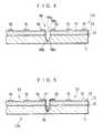
- FIG. 4is a partially-broken cross-sectional view of the substrate wafer illustrated in FIG. 3 .
- FIG. 5is a cross-sectional view which is similar to FIG. 4 and illustrates a process for forming a conductive layer in the substrate wafer illustrated in FIG. 3 .
- FIG. 6is a plan view which is similar to FIG. 1 and illustrates another semiconductor device relating to the present invention.
- FIG. 7is a cross-sectional view which is similar to FIG. 5 and illustrates a process for manufacturing the semiconductor device illustrated in FIG. 6 .
- FIG. 8is a cross-sectional view illustrating an example of packaging of the semiconductor device relating to the present invention.
- FIG. 9is a cross-sectional view illustrating a manufacturing process in a case in which the method of manufacturing a semiconductor device relating to the present invention is applied to a CSP, which is another example of packaging using a package plate.
- FIG. 10is a cross-sectional view illustrating a process of arranging a package plate and showing another example of a package plate utilized in a CSP relating to the present invention.
- FIG. 11is a cross-sectional view illustrating respective processes for forming cut grooves and a conductive layer in the CSP shown in FIG. 10 .
- FIGS. 1 and 2are a plan view and a cross-sectional view schematically illustrating a semiconductor chip 10 having an SOI structure relating to the present invention.
- an electronic circuitis formed within a silicon semiconductor crystal layer 13 which is layered on a silicon substrate 11 via an insulating layer 12 formed from, for example, silicon oxide.
- a conventionally known electronic circuit elementsuch as a unipolar transistor element like a MOS transistor, or a bipolar transistor, or the like is built-into the electronic circuit.
- the surface of the silicon crystal layer, i.e., the semiconductor layer 13 , into which the electronic circuit is builtis protected by a surface oxide film 14 which is formed from silicon oxide and covers the entire surface of the semiconductor layer 13 .
- a plurality of internal electrode pads 15are arranged at the central portion of the surface oxide film 14 , i.e., the portion other than the peripheral portion.
- a plurality of electrode pads 16 for the substrateare arranged at the peripheral portion of the surface oxide film 14 .
- the internal electrode pads 15 illustrated in FIG. 2penetrate through the surface oxide film 14 in the film thickness direction thereof, and, as is conventionally well known, are connected to connection terminals corresponding to the electronic circuit within the silicon crystal layer 13 .
- the electrode pads 16 for the substratedo not penetrate through the surface oxide film 14 , and rather, are supported on the surface oxide film 14 .
- a conductive layer 17is formed at the IC chip 10 from the substrate 11 toward the electrode pads 16 for the substrate, along the side surfaces of the silicon substrate 11 .
- the conductive layer 17is formed so as to surround the edge portions of the surface oxide film 14 , so as to be electrically connected to all of the electrode pads 16 for the substrate on the surface oxide film 14 . Further, the conductive layer 17 is formed so as to surround the peripheral side surfaces of the layered body ( 11 , 12 , 13 , 14 ) which includes the silicon substrate 11 , so as to surround the peripheral sides of the IC chip 10 .
- the conductive layer 17is formed from a metal material which is conductive and which hardens when heated, e.g., soldering paste or silver paste, as will be discussed later.
- the conductive layer 17surrounds the silicon crystal layer 13 and the silicon substrate 11 , and is connected to the silicon crystal layer 13 and the silicon substrate 11 over a wide surface area of contact.
- the conductive layer 17is also connected to the respective electrode pads 16 for the substrate.
- the electrode pads 16 for the substrate on the surface oxide film 14are reliably connected at a relatively low electrical resistance to the silicon crystal layer 13 beneath the surface oxide film 14 , and to the silicon substrate 11 beneath the insulating layer 12 which is beneath the silicon crystal layer 13 .
- the silicon crystal layer 13by applying a desired potential to the electrode pads 16 for the substrate which are formed on the surface oxide film 14 which is at the surface side of the IC chip 10 , the silicon crystal layer 13 , and thus the layered body ( 11 , 12 , 13 and 14 ), can be appropriately maintained at a predetermined potential, and the IC chip 10 can thereby be used in a stable operational state.
- the conductive layer 17is formed from a metal material and surrounds the peripheral sides of the IC chip 10 .
- the overall strength of the IC chip 10is high, and the durability of the IC chip 10 improves.
- a predetermined potentialcan be applied to the silicon substrate 11 from the surface side of the IC chip 10 without forming in the layered body ( 11 , 12 , 13 , 14 ) conventional holes formed by etching (hereinafter “etched holes”) which extend within the layered body which forms the chip main body.
- the silicon substrate 11 and the electrode pads 16 for the substratecan be connected compactly by the conductive layer 17 without lead wires, which extend from the silicon substrate 11 of the IC chip 10 to the electrode pads 16 for the substrate provided on the surface of the IC chip 10 , being disposed so as to protrude out greatly at the sides of the IC chip 10 .
- a desired potentialcan be suitably applied to the silicon substrate 11 without adversely affecting the compactness of the IC chip 10 .
- the layered body ( 11 , 12 , 13 , 14 ) at which the internal electrode pads 15 and the electrode pads 16 for the substrate are formed,is formed, in accordance with a conventionally known method for manufacturing a semiconductor, collectively on a wafer 11 A formed from a single silicon substrate as shown in FIG. 3 .
- cut grooves 18which extend to the silicon substrate 11 from the surface oxide film 14 via the silicon crystal layer 13 and the insulating layer 12 , are formed on the wafer 11 A.
- the cut grooves 18are formed in a lattice-like configuration along the borders of the respective IC chips 10 , and are called grid lines.
- the grid linei.e., the cut groove 18
- the grid lineis defined, between electrode pads 16 for the substrate of two adjacent IC chips 10 , by a pair of side wall surfaces 18 a which are spaced apart from each other and extend downward, and inclined bottom wall surfaces 18 b which extend downwardly from the bottom ends of the side wall surfaces and converge together.
- the inclined bottom wall surfaces 18 bdo not extend to the bottom surface of the silicon substrate 11 , and rather, converge at a position which is a slight distance away from the bottom surface of the silicon substrate 11 .
- the wafer 11 Ais in a half-cut state such that a thin thickness of the substrate 11 remains beneath the cut grooves 18 .
- cut grooves 18are formed by using, for example, a conventionally known scriber having a diamond cutter.
- a conductive, paste-like metal materialsuch as a solder paste or a silver paste, is applied to regions extending from the wall surfaces 18 a and 18 b of the groove to the electrode pads 16 for the substrate.
- the paste materialis subjected to an appropriate heating processing and thereby hardens.
- the conductive layer 17 connecting the electrode pads 16 for the substrate and the silicon substrate 11is formed continuously for each of the adjacent IC chips 10 .
- the wafer 11 Ais separated into the respective chips 10 along the cut grooves 18 . As the wafer 11 A is separated, the conductive layers 17 which are integral with the respective chips 10 are separated.
- the cut grooveswhich are grid lines for separating the respective IC chips and which are used in conventional methods for manufacturing semiconductors, are used as described above.
- a large number of IC chips, to which a substrate potential can be applied from the IC chip surfacecan be efficiently formed without forming special etched holes for connecting the electrode pads 16 for the substrate and the silicon substrate 11 , and without an etching process for forming the etched holes.
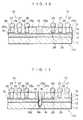
- FIGS. 6 and 7illustrate another semiconductor IC chip 10 relating to the present invention, and a method of manufacturing the same.
- the IC chip 10 illustrated in FIG. 6has an SOI structure which is a layered structure formed from the silicon substrate 11 , the insulating layer 12 , the silicon crystal layer 13 and the surface oxide film 14 , and the method of manufacturing thereof illustrated in FIG. 7 is basically the same as the method illustrated in FIG. 5 .
- the silicon crystal layer 13 in which the electronic circuit is built-inis electrically isolated on the insulating layer 12 by three insulating bands 19 a, 19 b, 19 c which are silicon oxide film layers formed by, for example, LOCOS or STI (shallow trench isolation).
- the silicon crystal layer 13 in which the electronic circuit is built-inis divided into circuit blocks 13 a, 13 b, 13 c, and a peripheral portion 13 d which surrounds these circuit blocks.
- the three circuit blocks 13 a, 13 b, 13 care for exclusive use for, for example, an analog circuit/digital circuit or a high speed operation circuit/low speed operation circuit, and these electronic circuits are built therein appropriately by conventionally known methods. Further, at the circuit blocks 13 a, 13 b, 13 c, the internal electrode pads 15 for the electronic circuits, such as those described above which are conventionally known, are provided on the surface oxide film 14 .
- a large number of electrode pads 16 for the substrateare arranged on the surface oxide film 14 at the peripheral portion of the silicon substrate 11 which surrounds all of the circuit blocks 13 a, 13 b, 13 c.
- the conductive layer 17 which connects the electrode pads 16 for the substrateis formed so as to surround the peripheral portion of the silicon substrate 11 .
- the electrode pad 16 for the substrateis reliably electrically connected to the peripheral portion 13 d of the silicon crystal layer 13 via a diffusion layer portion 20 which penetrates from the electrode pad 16 for the substrate through the surface oxide film 14 and extends into the peripheral portion 13 d of the silicon crystal layer 13 .
- the electrode pads 16 for the substrateare electrically connected to the silicon substrate 11 via the conductive layer 17 which surrounds the peripheral sides of the IC chip 10 .
- the peripheral portion 13 d of the silicon crystal layer 13can be reliably maintained at a predetermined potential in accordance with the silicon substrate 11 .
- the application of potential to the peripheral portion 13 dis effective in improving the anti-noise characteristic, as is known conventionally.
- the conductive layer 17which electrically connects the silicon substrate 11 to the electrode pads 16 for the substrate which are connected to the peripheral portion 13 d via the diffusion layer portions 20 , is formed in the cut grooves 18 which extend to the silicon substrate 11 and are for separating the large number of IC chips 10 which are collectively formed on the wafer 11 A which is similar to that described above. Namely, the conductive layer 17 is formed on the groove surfaces 18 a and 18 b. After the conductive layer 17 is formed, the wafer 11 A is separated into the respective IC chips 10 .
- FIG. 8illustrates an example of packaging the IC chip 10 .
- a recess 22i.e., a cavity
- the IC chip 10is accommodated such that the upper surface thereof, at which the electrode pads 16 of the substrate are provided, is positioned at the open end surface side of the recess 22 .
- Package electrodes 23 for electrical connection with the electrode pads 16 for the substrateare provided at the edge portion of the package body 21 which surrounds the recess 22 of the package body 21 .
- the internal portion electrode pads 15are not illustrated in FIG. 8 for the sake of convenience of illustration, package electrodes (not shown) for electrical connection with the internal portion electrode pads 15 are also provided at the edge portion of the package body 21 .
- the electrode pad 16 for the substratewhich is electrically connected to the silicon substrate 11 via the conductive layer 17 , is connected via a bonding wire 24 to the package electrode 23 which is positioned at the edge portion of the package body 21 at the same side of the package at which the electrode pad 16 for the substrate is provided.
- a conductive path which passes through the wall surface of the recess 22 of the package body 21is not formed as in the conventional art in order to apply potential to the silicon substrate 11 of the IC chip 10 .
- a predetermined potentialcan be applied to the silicon substrate 11 of the IC chip 10 .
- the electrode pad 16 for the substrate and the package electrode 23 connected theretoare positioned on the same side of the package. Therefore, the bonding wire 24 connecting the electrode pad 16 for the substrate and to the package electrode 23 can be provided compactly and does not have to be disposed in the interior of the recess 22 . Thus, the package can be made compact on the whole, and the manufacturing process does not become complex as compared to the conventional art.
- FIGS. 9 and 10illustrate an example in which the present invention is applied to a CSP.
- FIG. 9is a view, similar to FIGS. 5 and 7, which illustrates a method of manufacturing a CSP.
- An insulating plate 25which is formed from a polyimide resin material or the like, is joined, so as to face the surfaces of the IC chips 10 , to the wafer 11 A having the laminated structure in which the silicon substrate 11 , the insulating layer 12 , the silicon crystal layer 13 and the surface oxide film 14 are formed.
- Package plate portions 25 a corresponding to the respective IC chips 10are formed continuously at the insulating plate 25 .
- Slots 25 bare formed in the insulating plate 25 .
- the slots 25 bextend along the borders of the IC chips 10 and are for demarcating the package plate portions 25 a corresponding to the IC chips 10 .
- Conductive portions 26 and balls 27are formed at each of the package plate portions 25 a demarcated by the slots 25 b.
- the conductive portions 26are connected to the internal portion electrode pads 15 of the corresponding IC chip 10 , and penetrate through the insulating plate 25 in the direction of the plate thickness thereof.
- the balls 27are connection terminals which are connected to the conductive portion and are provided on the surface of the insulating plate 25 .
- the electrode pad 16 for electrical connection to the substrate 11 of the IC chip 10extends on the surface oxide film 14 of the IC chip 10 .
- the electrode pad 16 for the substrateis connected to a ball 29 via a conductive portion 28 which passes through the package plate portion 25 a.
- the balls 29are connection terminals which are aligned on the surface of the insulating plate 25 .
- the cut grooves 18are formed, in the same way as described above, along the slots 25 b. Thereafter, the conductive layer 17 , which electrically connects the electrode pads 16 for the substrate and the silicon substrate 11 , is formed along the groove surfaces of the cut grooves 18 as described previously. After the conductive layer 17 has been formed, the wafer 11 A is separated into the respective chips 10 along the cut grooves 18 . The respective conductive layers 17 are divided together with the chips 10 , so as to obtain the respective IC chips 10 having CSP structures.
- the electrode pads 16 for the substratecan be formed by filling in the portions corresponding to the slots 25 b with a conductive material.
- the electrode pad 16 for a substrateis connected to the ball 29 via a conductive portion 25 c which extends toward the ball 29 at the surface of the insulating plate 25 .
- the conductive portion 28does not serve as a conductor, but rather, functions as a holding portion for holding the ball 29 .
- the insulating plate 25in which the slots 25 b are filled in with the electrode pad 16 for the substrate, is joined to predetermined portions of the wafer 11 A as shown in FIG. 10 . Thereafter, the cut grooves 18 such as those described previously are formed from the insulating plate 25 side toward the silicon substrate 11 . As shown in FIG. 11, the cut grooves 18 extend to the silicon substrate 11 so as to divide the electrode pads 16 for the substrate which fill in the slots 25 b.
- the conductive layer 17similar to that described previously is formed in at the groove surfaces.
- the conductive layer 17extends to the electrode pads 16 for the substrate, via the groove surfaces 18 a and 18 b of the cut grooves 18 . Therefore, the silicon substrate 11 is electrically connected to the ball 29 which is connected to the pad 16 via the conductive portion 25 c.
- the wafer 11 Ais divided into the respective chips 10 along the cut grooves 18 .
- the conductive layers 17are divided together with the respective chips 10 , so as to obtain the IC chips 10 with CSP structures.
- the conductive layer 17surrounds the peripheral surfaces of the IC chip 10 continuously along the peripheral direction thereof.
- the conductive layer 17can be formed at portions in the peripheral direction of the IC chip 10 , i.e., can be formed non-continuously (intermittently).
- the conductive layer 17continuously in the peripheral direction of the IC chip 10 .
- the present inventionin terms of a semiconductor IC device having an SOI structure and a method of manufacturing the same.
- the present inventionis not limited to the same, and may be applied to a CMOS-LSI semiconductor device having a well portion which is a region electrically isolated from the substrate, and a method of manufacturing the same.
- the present inventionmay be applied to a dielectric isolated type LSI semiconductor device having a region which is electrically isolated from the substrate by a dielectric, and a method of manufacturing the same.
- the conductive layercan be formed at the groove surfaces of cut grooves by utilizing the cut grooves which are provided in order to separate the chips.
- the conductive layeris electrically connected to the substrate at the peripheral surfaces of the substrate without making the IC chip less compact. Therefore, a desired potential can be reliably and stably applied to the substrate.
- a semiconductor devicein which a stable substrate potential can be ensured without adversely affecting compactness, can be manufactured relatively easily.
- a conductive layer which is formed so as to surround the side surfaces of the substrateis used.
- the substrate and the electrode pads formed on the surface oxide film covering the substratecan be electrically connected well without using conductive plugs which extend within the IC chip and without using bonding wires which protrude outwardly of the chip by a large amount.
- the present inventionprovides a compact semiconductor device which exhibits stable operation due to a stable substrate potential being maintained.
Landscapes
- Engineering & Computer Science (AREA)
- Microelectronics & Electronic Packaging (AREA)
- Computer Hardware Design (AREA)
- Power Engineering (AREA)
- Physics & Mathematics (AREA)
- Condensed Matter Physics & Semiconductors (AREA)
- General Physics & Mathematics (AREA)
- Manufacturing & Machinery (AREA)
- Dicing (AREA)
- Internal Circuitry In Semiconductor Integrated Circuit Devices (AREA)
- Semiconductor Integrated Circuits (AREA)
Abstract
Description
1. Field of the Invention
The present invention relates to a semiconductor device and a method of manufacturing the same, and in particular, to a semiconductor device which is suited to an SOI structure and a method of manufacturing the same.
2. Description of the Related Art
One technique of manufacturing a semiconductor is the SOI (Semiconductor-On-Insulator) technique which is as follows. An insulating film (such as a silicon oxide film) which serves as a buffer layer is grown on an insulating substrate of silicon oxide or sapphire or the like. Thereafter, a semiconductor thin film is formed on the insulating film. For example, a unipolar transistor element such as a MOS transistor, or a bipolar transistor element is built-in in this semiconductor thin film. In a semiconductor device such as a semiconductor integrated circuit (IC) having an SOI structure formed by this SOI technique, the junction capacitance is lower than that of a semiconductor device formed at a bulk semiconductor. Thus, a semiconductor device having an SOI structure has advantages such as the operational speed of the semiconductor device is improved.
In such an IC, generally, a large number of the same IC portions are formed collectively on a substrate wafer. Pads, which are the connection terminals to the respective internal circuits, are formed on the surface of the substrate wafer for the respective IC portions. The IC portions of the substrate wafer are cut out and separated as chips by, for example, cleavage using scribe lines. In this way, the individual IC chips are formed.
The IC chips are packaged in order to facilitate handling thereof at the time the IC chip is assembled with a circuit board or the like. In a chip scale package (CSP), a package plate is used which is formed from an insulating plate made of, for example, polyimide, at which connection terminals corresponding to the respective pads are provided. In a CSP, before the wafer is separated into the IC chips, the surfaces of the IC chips are covered by the package plate so that the pads for the internal circuits provided at the wafer surface abut the connection terminals corresponding to the package plate.
Potential is applied to the IC substrate in order to ensure stable operation of the IC chip. In order to apply potential to the IC substrate, the following has been proposed. Pads for electrical connection to the IC substrate are provided on the IC chip surface opposing the package plate. (Hereinafter, these pads will be referred to as “pads for the substrate”.) Embedded plug portions, which extend from the pads through the interior of the IC chip toward the substrate, are formed.
In this way, conductive portions, which extend from the IC substrate to the pads for the substrate provided at the IC surface, are formed as embedded plug portions which extend through the interior of the IC chip. Thus, potential can be applied to the IC substrate from the IC chip surface which is at the same side at which the package plate is positioned and other pads for the internal circuit are provided, without leading to a substantial increase in the surface area required for the IC chip, i.e., without making the IC chip less compact.
However, in the above-described conventional structure, a special additional processing is required in order to form, by etching and within the main body of the IC chip, the holes for forming the embedded plug portions. Thus, manufacturing becomes complex. Further, the surface area of contact between the substrate and the embedded plug portion, which is embedded in the hole formed by etching, is determined by the hole diameter of the etched hole and the like, and is relatively small. Thus, the conventional structure is not preferable from the standpoint of reliable and stable application of potential.
In addition, the conventional structure affects the chip layout as well, and results in the semiconductor device being less compact.
An object of the present invention is to provide a semiconductor device which can be manufactured relatively easily and can ensure a stable substrate potential without a loss of compactness of the semiconductor device, and to provide a method of manufacturing the semiconductor device.
In order to achieve the above object, cut grooves are utilized in the present invention. The cut grooves are formed in a substrate wafer, at which semiconductor devices are collectively formed, for separating the substrate wafer into semiconductor chips of the respective semiconductor devices. A conductive layer, which extends to electrode pads for electrical connection to the substrate, is formed in the groove surface of the cut groove.
Namely, a method of manufacturing a semiconductor device according to the present invention includes the steps of: forming cut grooves in a wafer which becomes a substrate, the wafer including a semiconductor layer which is disposed on the wafer via an insulating layer and at which a plurality of same semiconductor circuits are formed collectively, a surface oxide film which covers the semiconductor layer, and electrode pads for electrical contact with the substrate, the electrode pads being formed on the surface oxide film in correspondence with the respective semiconductor circuits, the cut grooves being formed in the wafer from the surface oxide film to the substrate, for separating the wafer into chips of the respective semiconductor circuits; and before separating the wafer into the chips, forming a conductive layer on groove surfaces of the cut grooves, the conductive layer extending from a substrate region via the groove surfaces of the cut grooves to the electrode pads.
In accordance with the method relating to the present invention, the conductive layer, which connects the chip substrate positioned at the reverse surface side of the chip and the electrode pads for the substrate which are positioned at the front surface side of the chip, is not provided within the chip. There is no need to subject the inner portion of the chip to etching in order to form the conductive layer.
The conductive layer is formed at the groove surfaces of the cut grooves by using the cut grooves which are provided in order to separate the chips. Thus, no bonding wire projects outwardly of the IC chip to a great extent, as in the case in which bonding wires are used, and therefore, the dimensions of the IC chip do not substantially increase. Accordingly, the IC chip can be made compact.
Further, the conductive layer which connects the substrate and the electrode pads for the substrate is connected to the substrate at the peripheral side surface of the substrate. Therefore, as compared to a conventional method using embedded plug portions, the electrode pads can be connected to the substrate over a wider connection surface area. Thus, a desired potential can be stably and reliably applied to the substrate.
The cut grooves may be grid lines disposed in a lattice configuration on the substrate wafer for separating the wafer into the respective chips. Further, the conductive layer may be formed by heating after a paste-like conductive material which hardens by heating, e.g., solder paste or silver paste, is applied to predetermined places including the groove surfaces of the cut grooves.
In the method of manufacturing a semiconductor device according to the present invention, preferably, the wafer is formed from silicon oxide, and the silicon oxide, together with the insulating layer and the semiconductor layer, forms an SOI structure. Namely, the method of the present invention is suitable for manufacturing SOI devices. However, instead, the present invention may be applied to a CMOS-LSI having a wafer portion which is electrically isolated from the substrate via an insulating layer. Or, the present invention may be applied to an LSI which is electrically isolated from the substrate by a dielectric.
The semiconductor device relating to the present invention includes a substrate; a semiconductor layer which is disposed on said substrate via an insulating layer, and in which a semiconductor circuit is built in; a surface oxide film covering said semiconductor layer; an electrode pad which is provided on said surface oxide film and which is for electrical contact with said substrate; and a conductive layer for electrically connecting said electrode pad and said substrate, wherein said conductive layer surrounds peripheral surfaces of said semiconductor device including side surfaces of said substrate, and surrounds edge portions of said surface oxide film.
The conductive layer is formed so as to surround the side surfaces of the substrate. Thus, in order to connect the electrode pads and the substrate, there is no need to use a bonding wire which protrudes out to a great extent at the outer side of the semiconductor device, and there is no need for conventional conductive plugs which extend through the interior of the IC chip. Due to the conductive layer, the substrate and the electrode pads formed on the surface oxide film covering the substrate can be suitably connected together.
The conductive layer does not have to be formed continuously along the peripheral direction at the peripheral surfaces of the substrate, and may be formed intermittently along the peripheral direction of the substrate. In this way, portions of the side surfaces of the substrate along the peripheral direction thereof can be exposed from the conductive layer. However, in order to achieve more reliable electrical contact and to also protect the chip by the conductive layer, it is preferable that the conductive layer be formed continuously along the peripheral direction of the semiconductor device at the entire region of the side surfaces of the substrate and at the edge portions of the surface oxide film.
FIG. 1 is a plan view of a semiconductor device relating to the present invention.
FIG. 2 is a cross-sectional view taken along line II—II of FIG.1.
FIG. 3 is a plan view of a substrate wafer illustrating a process for forming grid lines in a substrate wafer at which semiconductor devices relating to the present invention are formed collectively.
FIG. 4 is a partially-broken cross-sectional view of the substrate wafer illustrated in FIG.3.
FIG. 5 is a cross-sectional view which is similar to FIG.4 and illustrates a process for forming a conductive layer in the substrate wafer illustrated in FIG.3.
FIG. 6 is a plan view which is similar to FIG.1 and illustrates another semiconductor device relating to the present invention.
FIG. 7 is a cross-sectional view which is similar to FIG.5 and illustrates a process for manufacturing the semiconductor device illustrated in FIG.6.
FIG. 8 is a cross-sectional view illustrating an example of packaging of the semiconductor device relating to the present invention.
FIG. 9 is a cross-sectional view illustrating a manufacturing process in a case in which the method of manufacturing a semiconductor device relating to the present invention is applied to a CSP, which is another example of packaging using a package plate.
FIG. 10 is a cross-sectional view illustrating a process of arranging a package plate and showing another example of a package plate utilized in a CSP relating to the present invention.
FIG. 11 is a cross-sectional view illustrating respective processes for forming cut grooves and a conductive layer in the CSP shown in FIG.10.
Hereinafter, an embodiment in which the present invention is applied to the manufacturing of a semiconductor IC chip having an SOI structure will be described in detail with reference to the drawings.
FIGS. 1 and 2 are a plan view and a cross-sectional view schematically illustrating asemiconductor chip 10 having an SOI structure relating to the present invention.
In theIC chip 10 having an SOI structure, as illustrated in FIG. 2, for example, an electronic circuit is formed within a siliconsemiconductor crystal layer 13 which is layered on asilicon substrate 11 via an insulatinglayer 12 formed from, for example, silicon oxide. As needed, a conventionally known electronic circuit element (not shown) such as a unipolar transistor element like a MOS transistor, or a bipolar transistor, or the like is built-into the electronic circuit.
The surface of the silicon crystal layer, i.e., thesemiconductor layer 13, into which the electronic circuit is built is protected by asurface oxide film 14 which is formed from silicon oxide and covers the entire surface of thesemiconductor layer 13. As illustrated in FIG. 1, a plurality ofinternal electrode pads 15 are arranged at the central portion of thesurface oxide film 14, i.e., the portion other than the peripheral portion. Further, a plurality ofelectrode pads 16 for the substrate are arranged at the peripheral portion of thesurface oxide film 14.
Theinternal electrode pads 15 illustrated in FIG. 2 penetrate through thesurface oxide film 14 in the film thickness direction thereof, and, as is conventionally well known, are connected to connection terminals corresponding to the electronic circuit within thesilicon crystal layer 13.
Theelectrode pads 16 for the substrate do not penetrate through thesurface oxide film 14, and rather, are supported on thesurface oxide film 14. As shown in FIG. 2, aconductive layer 17 is formed at theIC chip 10 from thesubstrate 11 toward theelectrode pads 16 for the substrate, along the side surfaces of thesilicon substrate 11.
As shown in FIG. 1, theconductive layer 17 is formed so as to surround the edge portions of thesurface oxide film 14, so as to be electrically connected to all of theelectrode pads 16 for the substrate on thesurface oxide film 14. Further, theconductive layer 17 is formed so as to surround the peripheral side surfaces of the layered body (11,12,13,14) which includes thesilicon substrate 11, so as to surround the peripheral sides of theIC chip 10.
Theconductive layer 17 is formed from a metal material which is conductive and which hardens when heated, e.g., soldering paste or silver paste, as will be discussed later.
Theconductive layer 17 surrounds thesilicon crystal layer 13 and thesilicon substrate 11, and is connected to thesilicon crystal layer 13 and thesilicon substrate 11 over a wide surface area of contact. Theconductive layer 17 is also connected to therespective electrode pads 16 for the substrate. Thus, theelectrode pads 16 for the substrate on thesurface oxide film 14 are reliably connected at a relatively low electrical resistance to thesilicon crystal layer 13 beneath thesurface oxide film 14, and to thesilicon substrate 11 beneath the insulatinglayer 12 which is beneath thesilicon crystal layer 13.
Accordingly, by applying a desired potential to theelectrode pads 16 for the substrate which are formed on thesurface oxide film 14 which is at the surface side of theIC chip 10, thesilicon crystal layer 13, and thus the layered body (11,12,13 and14), can be appropriately maintained at a predetermined potential, and theIC chip 10 can thereby be used in a stable operational state.
Further, theconductive layer 17 is formed from a metal material and surrounds the peripheral sides of theIC chip 10. Thus, the overall strength of theIC chip 10 is high, and the durability of theIC chip 10 improves.
At theIC chip 10 relating to the present invention, a predetermined potential can be applied to thesilicon substrate 11 from the surface side of theIC chip 10 without forming in the layered body (11,12,13,14) conventional holes formed by etching (hereinafter “etched holes”) which extend within the layered body which forms the chip main body. Further, thesilicon substrate 11 and theelectrode pads 16 for the substrate can be connected compactly by theconductive layer 17 without lead wires, which extend from thesilicon substrate 11 of theIC chip 10 to theelectrode pads 16 for the substrate provided on the surface of theIC chip 10, being disposed so as to protrude out greatly at the sides of theIC chip 10. Thus, a desired potential can be suitably applied to thesilicon substrate 11 without adversely affecting the compactness of theIC chip 10.
The method of manufacturing theIC chip 10 will be described hereinafter with reference to FIGS. 3 through 5.
The layered body (11,12,13,14) at which theinternal electrode pads 15 and theelectrode pads 16 for the substrate are formed, is formed, in accordance with a conventionally known method for manufacturing a semiconductor, collectively on awafer 11A formed from a single silicon substrate as shown in FIG.3.
As a pre-processing for separating thewafer 11A into therespective IC chips 10, cutgrooves 18, which extend to thesilicon substrate 11 from thesurface oxide film 14 via thesilicon crystal layer 13 and the insulatinglayer 12, are formed on thewafer 11A.
Thecut grooves 18 are formed in a lattice-like configuration along the borders of therespective IC chips 10, and are called grid lines.
As shown in FIG. 4, the grid line, i.e., thecut groove 18, is defined, betweenelectrode pads 16 for the substrate of twoadjacent IC chips 10, by a pair of side wall surfaces18awhich are spaced apart from each other and extend downward, and inclined bottom wall surfaces18bwhich extend downwardly from the bottom ends of the side wall surfaces and converge together. The inclined bottom wall surfaces18bdo not extend to the bottom surface of thesilicon substrate 11, and rather, converge at a position which is a slight distance away from the bottom surface of thesilicon substrate 11. Thus, thewafer 11A is in a half-cut state such that a thin thickness of thesubstrate 11 remains beneath thecut grooves 18.
These cutgrooves 18 are formed by using, for example, a conventionally known scriber having a diamond cutter.
After thecut grooves 18 are formed, a conductive, paste-like metal material, such as a solder paste or a silver paste, is applied to regions extending from the wall surfaces18aand18bof the groove to theelectrode pads 16 for the substrate.
The paste material is subjected to an appropriate heating processing and thereby hardens. Theconductive layer 17 connecting theelectrode pads 16 for the substrate and thesilicon substrate 11 is formed continuously for each of the adjacent IC chips10.
After theconductive layer 17 is formed, thewafer 11A is separated into therespective chips 10 along thecut grooves 18. As thewafer 11A is separated, theconductive layers 17 which are integral with therespective chips 10 are separated.
In accordance with the method relating to the present invention, the cut grooves, which are grid lines for separating the respective IC chips and which are used in conventional methods for manufacturing semiconductors, are used as described above. Thus, a large number of IC chips, to which a substrate potential can be applied from the IC chip surface, can be efficiently formed without forming special etched holes for connecting theelectrode pads 16 for the substrate and thesilicon substrate 11, and without an etching process for forming the etched holes.
FIGS. 6 and 7 illustrate anothersemiconductor IC chip 10 relating to the present invention, and a method of manufacturing the same.
In the same way as theIC chip 10 illustrated in FIG. 1, theIC chip 10 illustrated in FIG. 6 has an SOI structure which is a layered structure formed from thesilicon substrate 11, the insulatinglayer 12, thesilicon crystal layer 13 and thesurface oxide film 14, and the method of manufacturing thereof illustrated in FIG. 7 is basically the same as the method illustrated in FIG.5.
In theIC chip 10 illustrated in FIG. 6, thesilicon crystal layer 13 in which the electronic circuit is built-in is electrically isolated on the insulatinglayer 12 by three insulatingbands silicon crystal layer 13 in which the electronic circuit is built-in is divided into circuit blocks13a,13b,13c,and aperipheral portion 13dwhich surrounds these circuit blocks.
The threecircuit blocks internal electrode pads 15 for the electronic circuits, such as those described above which are conventionally known, are provided on thesurface oxide film 14.
Further, a large number ofelectrode pads 16 for the substrate are arranged on thesurface oxide film 14 at the peripheral portion of thesilicon substrate 11 which surrounds all of the circuit blocks13a,13b,13c.Theconductive layer 17 which connects theelectrode pads 16 for the substrate is formed so as to surround the peripheral portion of thesilicon substrate 11.
In the IC chip illustrated in FIG. 6, as is shown in FIG. 7 which illustrates the method of manufacturing thereof, theelectrode pad 16 for the substrate is reliably electrically connected to theperipheral portion 13dof thesilicon crystal layer 13 via adiffusion layer portion 20 which penetrates from theelectrode pad 16 for the substrate through thesurface oxide film 14 and extends into theperipheral portion 13dof thesilicon crystal layer 13.
Similarly to the example described above, theelectrode pads 16 for the substrate are electrically connected to thesilicon substrate 11 via theconductive layer 17 which surrounds the peripheral sides of theIC chip 10.
Accordingly, by applying a predetermined potential to theelectrode pads 16 for the substrate which are provided on the surface of theIC chip 10, theperipheral portion 13dof thesilicon crystal layer 13 can be reliably maintained at a predetermined potential in accordance with thesilicon substrate 11. The application of potential to theperipheral portion 13dis effective in improving the anti-noise characteristic, as is known conventionally.
As shown in FIG. 7 which is similar to FIG. 5, theconductive layer 17, which electrically connects thesilicon substrate 11 to theelectrode pads 16 for the substrate which are connected to theperipheral portion 13dvia thediffusion layer portions 20, is formed in thecut grooves 18 which extend to thesilicon substrate 11 and are for separating the large number ofIC chips 10 which are collectively formed on thewafer 11A which is similar to that described above. Namely, theconductive layer 17 is formed on the groove surfaces18aand18b.After theconductive layer 17 is formed, thewafer 11A is separated into the respective IC chips10.
FIG. 8 illustrates an example of packaging theIC chip 10.
In a recess22 (i.e., a cavity) of apackage body 21 which is formed from, for example, a mold or from ceramics and whose one end surface is open, theIC chip 10 is accommodated such that the upper surface thereof, at which theelectrode pads 16 of the substrate are provided, is positioned at the open end surface side of therecess 22.Package electrodes 23 for electrical connection with theelectrode pads 16 for the substrate are provided at the edge portion of thepackage body 21 which surrounds therecess 22 of thepackage body 21. Although the internalportion electrode pads 15 are not illustrated in FIG. 8 for the sake of convenience of illustration, package electrodes (not shown) for electrical connection with the internalportion electrode pads 15 are also provided at the edge portion of thepackage body 21.
Theelectrode pad 16 for the substrate, which is electrically connected to thesilicon substrate 11 via theconductive layer 17, is connected via abonding wire 24 to thepackage electrode 23 which is positioned at the edge portion of thepackage body 21 at the same side of the package at which theelectrode pad 16 for the substrate is provided.
Accordingly, in accordance with the package illustrated in FIG. 8, a conductive path which passes through the wall surface of therecess 22 of thepackage body 21 is not formed as in the conventional art in order to apply potential to thesilicon substrate 11 of theIC chip 10. By applying potential to thepackage electrodes 23, a predetermined potential can be applied to thesilicon substrate 11 of theIC chip 10.
Theelectrode pad 16 for the substrate and thepackage electrode 23 connected thereto are positioned on the same side of the package. Therefore, thebonding wire 24 connecting theelectrode pad 16 for the substrate and to thepackage electrode 23 can be provided compactly and does not have to be disposed in the interior of therecess 22. Thus, the package can be made compact on the whole, and the manufacturing process does not become complex as compared to the conventional art.
FIGS. 9 and 10 illustrate an example in which the present invention is applied to a CSP.
FIG. 9 is a view, similar to FIGS. 5 and 7, which illustrates a method of manufacturing a CSP.
An insulating plate25, which is formed from a polyimide resin material or the like, is joined, so as to face the surfaces of the IC chips10, to thewafer 11A having the laminated structure in which thesilicon substrate 11, the insulatinglayer 12, thesilicon crystal layer 13 and thesurface oxide film 14 are formed.Package plate portions 25acorresponding to therespective IC chips 10 are formed continuously at the insulating plate25.
In a vicinity of theslot 25bof thepackage plate portion 25a,theelectrode pad 16 for electrical connection to thesubstrate 11 of theIC chip 10 extends on thesurface oxide film 14 of theIC chip 10.
Theelectrode pad 16 for the substrate is connected to aball 29 via aconductive portion 28 which passes through thepackage plate portion 25a.In the same way as theballs 27, theballs 29 are connection terminals which are aligned on the surface of the insulating plate25.
After the insulating plate25 and thewafer 11A have been joined, thecut grooves 18 are formed, in the same way as described above, along theslots 25b.Thereafter, theconductive layer 17, which electrically connects theelectrode pads 16 for the substrate and thesilicon substrate 11, is formed along the groove surfaces of thecut grooves 18 as described previously. After theconductive layer 17 has been formed, thewafer 11A is separated into therespective chips 10 along thecut grooves 18. The respectiveconductive layers 17 are divided together with thechips 10, so as to obtain therespective IC chips 10 having CSP structures.
Instead of forming theslots 25bin the insulating plate25 as described above, as shown in FIG. 10, theelectrode pads 16 for the substrate can be formed by filling in the portions corresponding to theslots 25bwith a conductive material. Theelectrode pad 16 for a substrate is connected to theball 29 via aconductive portion 25cwhich extends toward theball 29 at the surface of the insulating plate25.
In this example, theconductive portion 28 does not serve as a conductor, but rather, functions as a holding portion for holding theball 29.
The insulating plate25, in which theslots 25bare filled in with theelectrode pad 16 for the substrate, is joined to predetermined portions of thewafer 11A as shown in FIG.10. Thereafter, thecut grooves 18 such as those described previously are formed from the insulating plate25 side toward thesilicon substrate 11. As shown in FIG. 11, thecut grooves 18 extend to thesilicon substrate 11 so as to divide theelectrode pads 16 for the substrate which fill in theslots 25b.
After thecut grooves 18 are formed, theconductive layer 17 similar to that described previously is formed in at the groove surfaces. Theconductive layer 17 extends to theelectrode pads 16 for the substrate, via the groove surfaces18aand18bof thecut grooves 18. Therefore, thesilicon substrate 11 is electrically connected to theball 29 which is connected to thepad 16 via theconductive portion 25c.
After theconductive layer 17 has been formed, in the same way as was explained with reference to FIG. 9, thewafer 11A is divided into therespective chips 10 along thecut grooves 18. As thewafer 11A is divided, theconductive layers 17 are divided together with therespective chips 10, so as to obtain the IC chips10 with CSP structures.
The above describes examples in which theconductive layer 17 surrounds the peripheral surfaces of theIC chip 10 continuously along the peripheral direction thereof. However, alternatively, theconductive layer 17 can be formed at portions in the peripheral direction of theIC chip 10, i.e., can be formed non-continuously (intermittently).
However, in order to obtain a reliable and good electrical connection between thesilicon substrate 11 and theelectrode pads 16 for the substrate and in order to increase the mechanical strength of theIC chip 10, it is preferable to form theconductive layer 17 continuously in the peripheral direction of theIC chip 10.
The above describes the present invention in terms of a semiconductor IC device having an SOI structure and a method of manufacturing the same. However, the present invention is not limited to the same, and may be applied to a CMOS-LSI semiconductor device having a well portion which is a region electrically isolated from the substrate, and a method of manufacturing the same. Or, the present invention may be applied to a dielectric isolated type LSI semiconductor device having a region which is electrically isolated from the substrate by a dielectric, and a method of manufacturing the same.
In accordance with the present invention, as described above, there is no need to subject the inner portions of the chip to etching processing in order to form a conductive layer which electrically connects the chip substrate and the electrode pads for the substrate. Further, the conductive layer can be formed at the groove surfaces of cut grooves by utilizing the cut grooves which are provided in order to separate the chips. Thus, the conductive layer is electrically connected to the substrate at the peripheral surfaces of the substrate without making the IC chip less compact. Therefore, a desired potential can be reliably and stably applied to the substrate.
Accordingly, in accordance with the method of the present invention, a semiconductor device, in which a stable substrate potential can be ensured without adversely affecting compactness, can be manufactured relatively easily.
In accordance with the present invention, a conductive layer which is formed so as to surround the side surfaces of the substrate is used. Thus, the substrate and the electrode pads formed on the surface oxide film covering the substrate can be electrically connected well without using conductive plugs which extend within the IC chip and without using bonding wires which protrude outwardly of the chip by a large amount. Thus, the present invention provides a compact semiconductor device which exhibits stable operation due to a stable substrate potential being maintained.
Claims (4)
1. A method of manufacturing a semiconductor device comprising the steps of:
forming cut grooves in a wafer which becomes a substrate, the wafer including a semiconductor layer which is disposed on the wafer via an insulating layer and at which a plurality of same semiconductor circuits are formed collectively, a surface oxide film which covers the semiconductor layer, and electrode pads for electrical contact with the substrate, the electrode pads being formed on the surface oxide film in correspondence with the respective semiconductor circuits, the cut grooves being formed in the wafer from the surface oxide film to the substrate, for separating the wafer into chips of the respective semiconductor circuits; and
before separating the wafer into the chips, forming a conductive layer on groove surfaces of the cut grooves, the conductive layer extending from a substrate region via the groove surfaces of the cut grooves to the electrode pads.
2. A method of manufacturing a semiconductor device according toclaim 1 , wherein the cut grooves are grid lines disposed in a lattice configuration.
3. A method of manufacturing a semiconductor device according toclaim 1 , wherein the conductive layer is formed by heating after a paste-like conductive material which hardens by heating is applied to predetermined places including the groove surfaces of the cut grooves.
4. A method of manufacturing a semiconductor device according toclaim 1 , wherein the wafer is formed from silicon oxide and, together with the insulating layer and the semiconductor layer, forms an SOI structure.
Applications Claiming Priority (2)
| Application Number | Priority Date | Filing Date | Title |
|---|---|---|---|
| JP11-257209 | 1999-09-10 | ||
| JP25720999AJP2001085361A (en) | 1999-09-10 | 1999-09-10 | Semiconductor device and manufacturing method |
Publications (1)
| Publication Number | Publication Date |
|---|---|
| US6379999B1true US6379999B1 (en) | 2002-04-30 |
Family
ID=17303186
Family Applications (1)
| Application Number | Title | Priority Date | Filing Date |
|---|---|---|---|
| US09/525,517Expired - Fee RelatedUS6379999B1 (en) | 1999-09-10 | 2000-03-15 | Semiconductor device and method of manufacturing the same |
Country Status (2)
| Country | Link |
|---|---|
| US (1) | US6379999B1 (en) |
| JP (1) | JP2001085361A (en) |
Cited By (31)
| Publication number | Priority date | Publication date | Assignee | Title |
|---|---|---|---|---|
| US6492196B1 (en)* | 2002-01-07 | 2002-12-10 | Picta Technology Inc. | Packaging process for wafer level IC device |
| US6586273B2 (en)* | 2000-12-12 | 2003-07-01 | Fujitsu Limited | Semiconductor device manufacturing method having a step of applying a copper foil on a substrate as a part of a wiring connecting an electrode pad to a mounting terminal |
| US20030232488A1 (en)* | 2002-06-14 | 2003-12-18 | Chua Swee Kwang | Wafer level packaging |
| US20040043603A1 (en)* | 2002-08-29 | 2004-03-04 | Wood Alan G. | Semiconductor component with backside contacts and method of fabrication |
| US6717245B1 (en)* | 2000-06-02 | 2004-04-06 | Micron Technology, Inc. | Chip scale packages performed by wafer level processing |
| US20040124523A1 (en)* | 2002-06-18 | 2004-07-01 | Poo Chia Yong | Semiconductor devices including peripherally located bond pads, intermediates thereof, assemblies, and packages including the semiconductor devices, and support elements for the semiconductor devices |
| US20040188400A1 (en)* | 2001-09-10 | 2004-09-30 | Micron Technology, Inc. | Wafer dicing device and method |
| US20040221451A1 (en)* | 2003-05-06 | 2004-11-11 | Micron Technology, Inc. | Method for packaging circuits and packaged circuits |
| US20050029668A1 (en)* | 2001-10-08 | 2005-02-10 | Micron Technology, Inc. | Apparatus and method for packaging circuits |
| US20050051844A1 (en)* | 2001-12-28 | 2005-03-10 | Rost Timothy A. | Versatile system for limiting mobile charge ingress in SOI semiconductor structures |
| US20050067680A1 (en)* | 2003-09-30 | 2005-03-31 | Boon Suan Jeung | Castellated chip-scale packages and methods for fabricating the same |
| US20060046436A1 (en)* | 2000-09-11 | 2006-03-02 | Shinji Ohuchi | Manufacturing method of stack-type semiconductor device |
| US20060081976A1 (en)* | 2003-09-30 | 2006-04-20 | Patel Chirag S | Fabrication of semiconductor dies with micro-pins and structures produced therewith |
| US20060118953A1 (en)* | 2002-03-06 | 2006-06-08 | Farnworth Warren M | Semiconductor component having thinned die with conductive vias |
| US20060275599A1 (en)* | 2003-01-10 | 2006-12-07 | Hugues Lefevre | Glazing comprising electronics elements |
| US7226809B2 (en) | 2002-06-18 | 2007-06-05 | Micron Technology, Inc. | Semiconductor devices and semiconductor device components with peripherally located, castellated contacts, assemblies and packages including such semiconductor devices or packages and associated methods |
| US20070145579A1 (en)* | 2005-12-09 | 2007-06-28 | Masataka Hoshino | Semiconductor device and method of manufacturing the same |
| US20070170577A1 (en)* | 2006-01-26 | 2007-07-26 | Infineon Technologies Ag | Semiconductor Device with Surface-Mountable External Contacts and Method for Manufacturing the Same |
| US20080174023A1 (en)* | 2007-01-23 | 2008-07-24 | Samsung Electronics Co., Ltd. | Chip having side pad, method of fabricating the same and package using the same |
| US20090011543A1 (en)* | 2007-07-03 | 2009-01-08 | Tjandra Winata Karta | Enhanced Reliability of Wafer-Level Chip-Scale Packaging (WLCSP) Die Separation Using Dry Etching |
| US20090020861A1 (en)* | 2007-07-18 | 2009-01-22 | Infineon Technologies Ag | Semiconductor device |
| US7511379B1 (en)* | 2006-03-23 | 2009-03-31 | National Semiconductor Corporation | Surface mountable direct chip attach device and method including integral integrated circuit |
| US7608919B1 (en) | 2003-09-04 | 2009-10-27 | University Of Notre Dame Du Lac | Interconnect packaging systems |
| US20100136747A1 (en)* | 2006-11-14 | 2010-06-03 | Samsung Electronics Co., Ltd. | Method for manufacturing semiconductor package |
| US20100244268A1 (en)* | 2006-06-29 | 2010-09-30 | Jiamiao Tang | Apparatus, system, and method for wireless connection in integrated circuit packages |
| US20100267204A1 (en)* | 2007-05-08 | 2010-10-21 | Mutual-Pak Technology Co., Ltd. | Package structure for integrated circuit device and method of the same |
| WO2010149762A3 (en)* | 2009-06-25 | 2011-04-21 | Imec | Biocompatible packaging |
| US20120032325A1 (en)* | 2005-10-03 | 2012-02-09 | Rohm Co., Ltd. | Semiconductor device |
| US20140145391A1 (en)* | 2011-05-06 | 2014-05-29 | Osram Opto Semiconductors Gmbh | Component carrier assembly having a trench structure which separates component carrier regions, and method for producing a plurality of component carrier regions |
| CN104428890A (en)* | 2012-07-11 | 2015-03-18 | 三菱电机株式会社 | Semiconductor device and manufacturing method thereof |
| US9620473B1 (en) | 2013-01-18 | 2017-04-11 | University Of Notre Dame Du Lac | Quilt packaging system with interdigitated interconnecting nodules for inter-chip alignment |
Citations (14)
| Publication number | Priority date | Publication date | Assignee | Title |
|---|---|---|---|---|
| US5202754A (en) | 1991-09-13 | 1993-04-13 | International Business Machines Corporation | Three-dimensional multichip packages and methods of fabrication |
| US5646067A (en)* | 1995-06-05 | 1997-07-08 | Harris Corporation | Method of bonding wafers having vias including conductive material |
| US5879964A (en)* | 1997-07-07 | 1999-03-09 | Korea Advanced Institute Of Science And Technology | Method for fabricating chip size packages using lamination process |
| US6020217A (en)* | 1997-02-21 | 2000-02-01 | Daimler-Benz Aktiengesellschaft | Semiconductor devices with CSP packages and method for making them |
| US6080603A (en)* | 1994-07-07 | 2000-06-27 | Tessera, Inc. | Fixtures and methods for lead bonding and deformation |
| US6107164A (en)* | 1998-08-18 | 2000-08-22 | Oki Electric Industry Co., Ltd. | Using grooves as alignment marks when dicing an encapsulated semiconductor wafer |
| US6117347A (en)* | 1996-07-10 | 2000-09-12 | Nec Corporation | Method of separating wafers into individual die |
| US6117704A (en)* | 1999-03-31 | 2000-09-12 | Irvine Sensors Corporation | Stackable layers containing encapsulated chips |
| US6153448A (en)* | 1997-05-14 | 2000-11-28 | Kabushiki Kaisha Toshiba | Semiconductor device manufacturing method |
| US6197616B1 (en)* | 1998-11-27 | 2001-03-06 | Sanyo Electric Co., Ltd. | Method of fabricating semiconductor device |
| US6207477B1 (en)* | 1997-08-06 | 2001-03-27 | Fujitsu Limited | Semiconductor device having a ball grid array and a fabrication process thereof |
| US6221751B1 (en)* | 1997-01-24 | 2001-04-24 | Chipscale, Inc. | Wafer fabrication of die-bottom contacts for electronic devices |
| US6245646B1 (en)* | 1999-04-16 | 2001-06-12 | Micron Technology, Inc. | Film frame substrate fixture |
| US6245596B1 (en)* | 1998-03-19 | 2001-06-12 | Mitsubishi Denki Kabushiki Kaisha | Method of producing semiconductor device with heat dissipation metal layer and metal projections |
- 1999
- 1999-09-10JPJP25720999Apatent/JP2001085361A/enactivePending
- 2000
- 2000-03-15USUS09/525,517patent/US6379999B1/ennot_activeExpired - Fee Related
Patent Citations (14)
| Publication number | Priority date | Publication date | Assignee | Title |
|---|---|---|---|---|
| US5202754A (en) | 1991-09-13 | 1993-04-13 | International Business Machines Corporation | Three-dimensional multichip packages and methods of fabrication |
| US6080603A (en)* | 1994-07-07 | 2000-06-27 | Tessera, Inc. | Fixtures and methods for lead bonding and deformation |
| US5646067A (en)* | 1995-06-05 | 1997-07-08 | Harris Corporation | Method of bonding wafers having vias including conductive material |
| US6117347A (en)* | 1996-07-10 | 2000-09-12 | Nec Corporation | Method of separating wafers into individual die |
| US6221751B1 (en)* | 1997-01-24 | 2001-04-24 | Chipscale, Inc. | Wafer fabrication of die-bottom contacts for electronic devices |
| US6020217A (en)* | 1997-02-21 | 2000-02-01 | Daimler-Benz Aktiengesellschaft | Semiconductor devices with CSP packages and method for making them |
| US6153448A (en)* | 1997-05-14 | 2000-11-28 | Kabushiki Kaisha Toshiba | Semiconductor device manufacturing method |
| US5879964A (en)* | 1997-07-07 | 1999-03-09 | Korea Advanced Institute Of Science And Technology | Method for fabricating chip size packages using lamination process |
| US6207477B1 (en)* | 1997-08-06 | 2001-03-27 | Fujitsu Limited | Semiconductor device having a ball grid array and a fabrication process thereof |
| US6245596B1 (en)* | 1998-03-19 | 2001-06-12 | Mitsubishi Denki Kabushiki Kaisha | Method of producing semiconductor device with heat dissipation metal layer and metal projections |
| US6107164A (en)* | 1998-08-18 | 2000-08-22 | Oki Electric Industry Co., Ltd. | Using grooves as alignment marks when dicing an encapsulated semiconductor wafer |
| US6197616B1 (en)* | 1998-11-27 | 2001-03-06 | Sanyo Electric Co., Ltd. | Method of fabricating semiconductor device |
| US6117704A (en)* | 1999-03-31 | 2000-09-12 | Irvine Sensors Corporation | Stackable layers containing encapsulated chips |
| US6245646B1 (en)* | 1999-04-16 | 2001-06-12 | Micron Technology, Inc. | Film frame substrate fixture |
Cited By (111)
| Publication number | Priority date | Publication date | Assignee | Title |
|---|---|---|---|---|
| US20070148918A1 (en)* | 2000-06-02 | 2007-06-28 | Kinsman Larry D | Method for fabricating a chip scale package using wafer level processing |
| US6900079B2 (en) | 2000-06-02 | 2005-05-31 | Micron Technology, Inc. | Method for fabricating a chip scale package using wafer level processing |
| US7183191B2 (en) | 2000-06-02 | 2007-02-27 | Micron Technology, Inc. | Method for fabricating a chip scale package using wafer level processing |
| US7727858B2 (en) | 2000-06-02 | 2010-06-01 | Micron Technology, Inc. | Method for fabricating a chip scale package using wafer level processing |
| US20050164429A1 (en)* | 2000-06-02 | 2005-07-28 | Kinsman Larry D. | Method for fabricating a chip scale package using wafer level processing |
| US6780746B2 (en) | 2000-06-02 | 2004-08-24 | Micron Technology, Inc. | Method for fabricating a chip scale package using wafer level processing and devices resulting therefrom |
| US6717245B1 (en)* | 2000-06-02 | 2004-04-06 | Micron Technology, Inc. | Chip scale packages performed by wafer level processing |
| US20040126928A1 (en)* | 2000-06-02 | 2004-07-01 | Kinsman Larry D. | Method for fabricating a chip scale package using wafer level processing and devices resulting therefrom |
| US20060046436A1 (en)* | 2000-09-11 | 2006-03-02 | Shinji Ohuchi | Manufacturing method of stack-type semiconductor device |
| US7405138B2 (en)* | 2000-09-11 | 2008-07-29 | Oki Electric Industry Co., Ltd. | Manufacturing method of stack-type semiconductor device |
| US6967399B2 (en) | 2000-12-12 | 2005-11-22 | Fujitsu Limited | Semiconductor device manufacturing method having a step of applying a copper foil on a substrate as a part of a wiring connecting an electrode pad to a mounting terminal |
| US20030207574A1 (en)* | 2000-12-12 | 2003-11-06 | Fujitsu Limited | Semiconductor device manufacturing method having a step of applying a copper foil on a substrate as a part of a wiring connecting an electrode pad to a mounting terminal |
| US6586273B2 (en)* | 2000-12-12 | 2003-07-01 | Fujitsu Limited | Semiconductor device manufacturing method having a step of applying a copper foil on a substrate as a part of a wiring connecting an electrode pad to a mounting terminal |
| US20040188400A1 (en)* | 2001-09-10 | 2004-09-30 | Micron Technology, Inc. | Wafer dicing device and method |
| US8138617B2 (en) | 2001-10-08 | 2012-03-20 | Round Rock Research, Llc | Apparatus and method for packaging circuits |
| US7358154B2 (en) | 2001-10-08 | 2008-04-15 | Micron Technology, Inc. | Method for fabricating packaged die |
| US20080054423A1 (en)* | 2001-10-08 | 2008-03-06 | Micron Technology, Inc. | Apparatus and method for packaging circuits |
| US6894386B2 (en)* | 2001-10-08 | 2005-05-17 | Micron Technology, Inc. | Apparatus and method for packaging circuits |
| US20050029668A1 (en)* | 2001-10-08 | 2005-02-10 | Micron Technology, Inc. | Apparatus and method for packaging circuits |
| US7675169B2 (en) | 2001-10-08 | 2010-03-09 | Micron Technology, Inc. | Apparatus and method for packaging circuits |
| US20100140794A1 (en)* | 2001-10-08 | 2010-06-10 | Chia Yong Poo | Apparatus and method for packaging circuits |
| US20060084240A1 (en)* | 2001-10-08 | 2006-04-20 | Micron Technology, Inc. | Apparatus and method for packaging circuits |
| US8115306B2 (en) | 2001-10-08 | 2012-02-14 | Round Rock Research, Llc | Apparatus and method for packaging circuits |
| US20050051844A1 (en)* | 2001-12-28 | 2005-03-10 | Rost Timothy A. | Versatile system for limiting mobile charge ingress in SOI semiconductor structures |
| US7148558B2 (en)* | 2001-12-28 | 2006-12-12 | Texas Instruments Incorporated | Versatile system for limiting mobile charge ingress in SOI semiconductor structures |
| US6492196B1 (en)* | 2002-01-07 | 2002-12-10 | Picta Technology Inc. | Packaging process for wafer level IC device |
| US20060118953A1 (en)* | 2002-03-06 | 2006-06-08 | Farnworth Warren M | Semiconductor component having thinned die with conductive vias |
| US7417325B2 (en) | 2002-03-06 | 2008-08-26 | Micron Technology, Inc. | Semiconductor component having thinned die with conductive vias configured as conductive pin terminal contacts |
| US20110018143A1 (en)* | 2002-06-14 | 2011-01-27 | Swee Kwang Chua | Wafer level packaging |
| US8106488B2 (en) | 2002-06-14 | 2012-01-31 | Micron Technology, Inc. | Wafer level packaging |
| US20030232488A1 (en)* | 2002-06-14 | 2003-12-18 | Chua Swee Kwang | Wafer level packaging |
| US7375009B2 (en) | 2002-06-14 | 2008-05-20 | Micron Technology, Inc. | Method of forming a conductive via through a wafer |
| US8564106B2 (en) | 2002-06-14 | 2013-10-22 | Micron Technology, Inc. | Wafer level packaging |
| US7285850B2 (en) | 2002-06-18 | 2007-10-23 | Micron Technology, Inc. | Support elements for semiconductor devices with peripherally located bond pads |
| US20040124523A1 (en)* | 2002-06-18 | 2004-07-01 | Poo Chia Yong | Semiconductor devices including peripherally located bond pads, intermediates thereof, assemblies, and packages including the semiconductor devices, and support elements for the semiconductor devices |
| US7115984B2 (en) | 2002-06-18 | 2006-10-03 | Micron Technology, Inc. | Semiconductor devices including peripherally located bond pads, intermediates thereof, assemblies, and packages including the semiconductor devices, and support elements for the semiconductor devices |
| US20060208351A1 (en)* | 2002-06-18 | 2006-09-21 | Poo Chia Y | Semiconductor devices including peripherally located bond pads, intermediates thereof, and assemblies and packages including the semiconductor devices |
| US20060208350A1 (en)* | 2002-06-18 | 2006-09-21 | Poo Chia Y | Support elements for semiconductor devices with peripherally located bond pads |
| US7226809B2 (en) | 2002-06-18 | 2007-06-05 | Micron Technology, Inc. | Semiconductor devices and semiconductor device components with peripherally located, castellated contacts, assemblies and packages including such semiconductor devices or packages and associated methods |
| US20040041260A1 (en)* | 2002-08-29 | 2004-03-04 | Wood Alan G. | Semiconductor component with backside contacts and method of fabrication |
| US20040043603A1 (en)* | 2002-08-29 | 2004-03-04 | Wood Alan G. | Semiconductor component with backside contacts and method of fabrication |
| US6903442B2 (en) | 2002-08-29 | 2005-06-07 | Micron Technology, Inc. | Semiconductor component having backside pin contacts |
| US20060154446A1 (en)* | 2002-08-29 | 2006-07-13 | Wood Alan G | Method for fabricating semiconductor component with thnned substrate having pin contacts |
| US7132731B2 (en) | 2002-08-29 | 2006-11-07 | Micron Technology, Inc. | Semiconductor component and assembly having female conductive members |
| US20060006520A1 (en)* | 2002-08-29 | 2006-01-12 | Wood Alan G | Semiconductor component and system having back side and circuit side contacts |
| US7081665B2 (en) | 2002-08-29 | 2006-07-25 | Micron Technology, Inc. | Semiconductor component having thinned substrate, backside pin contacts and circuit side contacts |
| US7473582B2 (en) | 2002-08-29 | 2009-01-06 | Micron Technology, Inc. | Method for fabricating semiconductor component with thinned substrate having pin contacts |
| US20050029650A1 (en)* | 2002-08-29 | 2005-02-10 | Wood Alan G. | Method for fabricating semiconductor components with thinned substrate, back side contacts and circuit side contacts |
| US6828175B2 (en)* | 2002-08-29 | 2004-12-07 | Micron Technology, Inc. | Semiconductor component with backside contacts and method of fabrication |
| US20040207081A1 (en)* | 2002-08-29 | 2004-10-21 | Wood Alan G. | Semiconductor component having thinned substrate, backside pin contacts and circuit side contacts |
| US7078266B2 (en) | 2002-08-29 | 2006-07-18 | Micron Technology, Inc. | Method for fabricating semiconductor components with thinned substrate, back side contacts and circuit side contacts |
| US7745838B2 (en)* | 2003-01-10 | 2010-06-29 | Agc Glass Europe | Glazing comprising electronics elements |
| US20060275599A1 (en)* | 2003-01-10 | 2006-12-07 | Hugues Lefevre | Glazing comprising electronics elements |
| US8065792B2 (en) | 2003-05-06 | 2011-11-29 | Micron Technology, Inc. | Method for packaging circuits |
| US8555495B2 (en) | 2003-05-06 | 2013-10-15 | Micron Technology, Inc. | Method for packaging circuits |
| US20040221451A1 (en)* | 2003-05-06 | 2004-11-11 | Micron Technology, Inc. | Method for packaging circuits and packaged circuits |
| US10811278B2 (en) | 2003-05-06 | 2020-10-20 | Micron Technology, Inc. | Method for packaging circuits |
| US7712211B2 (en) | 2003-05-06 | 2010-05-11 | Micron Technology, Inc. | Method for packaging circuits and packaged circuits |
| US10453704B2 (en) | 2003-05-06 | 2019-10-22 | Micron Technology, Inc. | Method for packaging circuits |
| US9484225B2 (en) | 2003-05-06 | 2016-11-01 | Micron Technology, Inc. | Method for packaging circuits |
| US20100146780A1 (en)* | 2003-05-06 | 2010-06-17 | Yong Poo Chia | Method for packaging circuits and packaged circuits |
| US8623700B1 (en) | 2003-09-04 | 2014-01-07 | University Of Notre Dame Du Lac | Inter-chip communication |
| US7608919B1 (en) | 2003-09-04 | 2009-10-27 | University Of Notre Dame Du Lac | Interconnect packaging systems |
| US7612443B1 (en) | 2003-09-04 | 2009-11-03 | University Of Notre Dame Du Lac | Inter-chip communication |
| US8021965B1 (en) | 2003-09-04 | 2011-09-20 | University Of Norte Dame Du Lac | Inter-chip communication |
| US10410989B2 (en) | 2003-09-04 | 2019-09-10 | University Of Notre Dame Du Lac | Inter-chip alignment |
| US20100072603A1 (en)* | 2003-09-30 | 2010-03-25 | Micron Technology, Inc. | Semiconductor device assemblies and packages with edge contacts and sacrificial substrates and other intermediate structures used or formed in fabricating the assemblies or packages |
| US7633159B2 (en) | 2003-09-30 | 2009-12-15 | Micron Technology, Inc. | Semiconductor device assemblies and packages with edge contacts and sacrificial substrates and other intermediate structures used or formed in fabricating the assemblies or packages |
| US20050067680A1 (en)* | 2003-09-30 | 2005-03-31 | Boon Suan Jeung | Castellated chip-scale packages and methods for fabricating the same |
| US20060006521A1 (en)* | 2003-09-30 | 2006-01-12 | Boon Suan J | Semiconductor device assemblies and packages with edge contacts and sacrificial substrates and other intermediate structures used or formed in fabricating the assemblies or packages |
| US20060081976A1 (en)* | 2003-09-30 | 2006-04-20 | Patel Chirag S | Fabrication of semiconductor dies with micro-pins and structures produced therewith |
| US7208335B2 (en)* | 2003-09-30 | 2007-04-24 | Micron Technology, Inc. | Castellated chip-scale packages and methods for fabricating the same |
| US8063493B2 (en) | 2003-09-30 | 2011-11-22 | Micron Technology, Inc. | Semiconductor device assemblies and packages |
| US8432046B2 (en)* | 2005-10-03 | 2013-04-30 | Rohm Co., Ltd. | Semiconductor device |
| US20120032325A1 (en)* | 2005-10-03 | 2012-02-09 | Rohm Co., Ltd. | Semiconductor device |
| US9293441B2 (en) | 2005-12-09 | 2016-03-22 | Cypress Semiconductor Corporation | Semiconductor device and method of manufacturing the same |
| US7605457B2 (en)* | 2005-12-09 | 2009-10-20 | Spansion Llc | Semiconductor device and method of manufacturing the same |
| US20070145579A1 (en)* | 2005-12-09 | 2007-06-28 | Masataka Hoshino | Semiconductor device and method of manufacturing the same |
| US20070170577A1 (en)* | 2006-01-26 | 2007-07-26 | Infineon Technologies Ag | Semiconductor Device with Surface-Mountable External Contacts and Method for Manufacturing the Same |
| US7719101B2 (en)* | 2006-01-26 | 2010-05-18 | Infineon Technologies Ag | Semiconductor device with surface-mountable external contacts and method for manufacturing the same |
| US7713785B1 (en) | 2006-03-23 | 2010-05-11 | National Semiconductor Corporation | Surface mountable direct chip attach device and method including integral integrated circuit |
| US7511379B1 (en)* | 2006-03-23 | 2009-03-31 | National Semiconductor Corporation | Surface mountable direct chip attach device and method including integral integrated circuit |
| US9837340B2 (en) | 2006-06-29 | 2017-12-05 | Intel Corporation | Apparatus, system, and method for wireless connection in integrated circuit packages |
| US8084867B2 (en)* | 2006-06-29 | 2011-12-27 | Intel Corporation | Apparatus, system, and method for wireless connection in integrated circuit packages |
| US9385094B2 (en) | 2006-06-29 | 2016-07-05 | Intel Corporation | Apparatus, system, and method for wireless connection in integrated circuit packages |
| US8981573B2 (en) | 2006-06-29 | 2015-03-17 | Intel Corporation | Apparatus, system, and method for wireless connection in integrated circuit packages |
| US20120108053A1 (en)* | 2006-06-29 | 2012-05-03 | Jiamiao Tang | Apparatus, system, and method for wireless connection in integrated circuit packages |
| US8963333B2 (en) | 2006-06-29 | 2015-02-24 | Intel Corporation | Apparatus, system, and method for wireless connection in integrated circuit packages |
| US20100244268A1 (en)* | 2006-06-29 | 2010-09-30 | Jiamiao Tang | Apparatus, system, and method for wireless connection in integrated circuit packages |
| US8513108B2 (en)* | 2006-06-29 | 2013-08-20 | Intel Corporation | Apparatus, system, and method for wireless connection in integrated circuit packages |
| US20100136747A1 (en)* | 2006-11-14 | 2010-06-03 | Samsung Electronics Co., Ltd. | Method for manufacturing semiconductor package |
| US7791173B2 (en)* | 2007-01-23 | 2010-09-07 | Samsung Electronics Co., Ltd. | Chip having side pad, method of fabricating the same and package using the same |
| US20080174023A1 (en)* | 2007-01-23 | 2008-07-24 | Samsung Electronics Co., Ltd. | Chip having side pad, method of fabricating the same and package using the same |
| US20100267204A1 (en)* | 2007-05-08 | 2010-10-21 | Mutual-Pak Technology Co., Ltd. | Package structure for integrated circuit device and method of the same |
| US20090011543A1 (en)* | 2007-07-03 | 2009-01-08 | Tjandra Winata Karta | Enhanced Reliability of Wafer-Level Chip-Scale Packaging (WLCSP) Die Separation Using Dry Etching |
| US7838424B2 (en)* | 2007-07-03 | 2010-11-23 | Taiwan Semiconductor Manufacturing Company, Ltd. | Enhanced reliability of wafer-level chip-scale packaging (WLCSP) die separation using dry etching |
| US20090020861A1 (en)* | 2007-07-18 | 2009-01-22 | Infineon Technologies Ag | Semiconductor device |
| US8324739B2 (en) | 2007-07-18 | 2012-12-04 | Infineon Technologies Ag | Semiconductor device |
| US8343811B2 (en) | 2007-07-18 | 2013-01-01 | Infineon Technologies Ag | Semiconductor device |
| US20110096519A1 (en)* | 2007-07-18 | 2011-04-28 | Infineon Technologies Ag | Semiconductor device |
| US7893545B2 (en)* | 2007-07-18 | 2011-02-22 | Infineon Technologies Ag | Semiconductor device |
| US8658472B2 (en) | 2007-07-18 | 2014-02-25 | Infineon Technologies Ag | Semiconductor device |
| US20110097855A1 (en)* | 2007-07-18 | 2011-04-28 | Infineon Technologies Ag | Semiconductor device |
| US9048198B2 (en) | 2009-06-25 | 2015-06-02 | Imec | Biocompatible packaging |
| WO2010149762A3 (en)* | 2009-06-25 | 2011-04-21 | Imec | Biocompatible packaging |
| US10271796B2 (en) | 2009-06-25 | 2019-04-30 | Imec | Biocompatible packaging |
| US20140145391A1 (en)* | 2011-05-06 | 2014-05-29 | Osram Opto Semiconductors Gmbh | Component carrier assembly having a trench structure which separates component carrier regions, and method for producing a plurality of component carrier regions |
| US9623527B2 (en)* | 2011-05-06 | 2017-04-18 | Osram Opto Semiconductors Gmbh | Component carrier assembly having a trench structure which separates component carrier regions, and method for producing a plurality of component carrier regions |
| US9543252B2 (en) | 2012-07-11 | 2017-01-10 | Mitsubishi Electric Corporation | Semiconductor apparatus and method for producing the same |
| CN104428890A (en)* | 2012-07-11 | 2015-03-18 | 三菱电机株式会社 | Semiconductor device and manufacturing method thereof |
| US9620473B1 (en) | 2013-01-18 | 2017-04-11 | University Of Notre Dame Du Lac | Quilt packaging system with interdigitated interconnecting nodules for inter-chip alignment |
Also Published As
| Publication number | Publication date |
|---|---|
| JP2001085361A (en) | 2001-03-30 |
Similar Documents
| Publication | Publication Date | Title |
|---|---|---|
| US6379999B1 (en) | Semiconductor device and method of manufacturing the same | |
| US10141264B2 (en) | Method and structure for wafer level packaging with large contact area | |
| US8710648B2 (en) | Wafer level packaging structure with large contact area and preparation method thereof | |
| US7498636B2 (en) | Semiconductor device and method of manufacturing the same | |
| CN109192718B (en) | Multi-wafer bonding structure and bonding method | |
| US6590257B2 (en) | Semiconductor device and method for manufacturing the same, semiconductor wafer and semiconductor device manufactured thereby | |
| US6906415B2 (en) | Semiconductor device assemblies and packages including multiple semiconductor devices and methods | |
| US6343019B1 (en) | Apparatus and method of stacking die on a substrate | |
| TWI466250B (en) | Large soldering area wafer level package structure and the fabrication method thereof | |
| US8410599B2 (en) | Power MOSFET package | |
| US5668409A (en) | Integrated circuit with edge connections and method | |
| US6022797A (en) | Method of manufacturing through holes in a semiconductor device | |
| JP2006310726A (en) | Semiconductor device and manufacturing method thereof | |
| US20090206466A1 (en) | Semiconductor device | |
| US6746956B1 (en) | Hermetic seal for silicon die with metal feed through structure | |
| KR101247425B1 (en) | Semiconductor device and method for manufacturing the semiconductor device | |
| US6133625A (en) | Semiconductor device and method for manufacturing the same | |
| TWI861128B (en) | Semiconductor devices and methods of manufacturing semiconductor devices | |
| JP3632024B2 (en) | Chip package and manufacturing method thereof | |
| JP2003017495A (en) | Semiconductor device and method of manufacturing the same | |
| US7492009B2 (en) | Semiconductor device having silicon on insulator structure and method of fabricating the same | |
| KR100752665B1 (en) | Semiconductor device using conductive adhesive layer and its manufacturing method | |
| JP4754105B2 (en) | Semiconductor device and manufacturing method thereof | |
| US5187558A (en) | Stress reduction structure for a resin sealed semiconductor device | |
| JP2005033105A (en) | Semiconductor device and manufacturing method thereof, circuit board, and electronic apparatus |
Legal Events
| Date | Code | Title | Description |
|---|---|---|---|
| AS | Assignment | Owner name:OKI ELECTRIC INDUSTRY CO., LTD., JAPAN Free format text:ASSIGNMENT OF ASSIGNORS INTEREST;ASSIGNOR:TANABE, SHINJI;REEL/FRAME:010634/0034 Effective date:20000225 | |
| FPAY | Fee payment | Year of fee payment:4 | |
| AS | Assignment | Owner name:OKI SEMICONDUCTOR CO., LTD., JAPAN Free format text:CHANGE OF NAME;ASSIGNOR:OKI ELECTRIC INDUSTRY CO., LTD.;REEL/FRAME:022399/0969 Effective date:20081001 Owner name:OKI SEMICONDUCTOR CO., LTD.,JAPAN Free format text:CHANGE OF NAME;ASSIGNOR:OKI ELECTRIC INDUSTRY CO., LTD.;REEL/FRAME:022399/0969 Effective date:20081001 | |
| FPAY | Fee payment | Year of fee payment:8 | |
| REMI | Maintenance fee reminder mailed | ||
| LAPS | Lapse for failure to pay maintenance fees | ||
| STCH | Information on status: patent discontinuation | Free format text:PATENT EXPIRED DUE TO NONPAYMENT OF MAINTENANCE FEES UNDER 37 CFR 1.362 | |
| FP | Lapsed due to failure to pay maintenance fee | Effective date:20140430 |