US6376868B1 - Multi-layered gate for a CMOS imager - Google Patents
Multi-layered gate for a CMOS imagerDownload PDFInfo
- Publication number
- US6376868B1 US6376868B1US09/333,011US33301199AUS6376868B1US 6376868 B1US6376868 B1US 6376868B1US 33301199 AUS33301199 AUS 33301199AUS 6376868 B1US6376868 B1US 6376868B1
- Authority
- US
- United States
- Prior art keywords
- pixel sensor
- sensor cell
- gate
- layer
- spacers
- Prior art date
- Legal status (The legal status is an assumption and is not a legal conclusion. Google has not performed a legal analysis and makes no representation as to the accuracy of the status listed.)
- Expired - Lifetime
Links
Images


Classifications
- H—ELECTRICITY
- H10—SEMICONDUCTOR DEVICES; ELECTRIC SOLID-STATE DEVICES NOT OTHERWISE PROVIDED FOR
- H10F—INORGANIC SEMICONDUCTOR DEVICES SENSITIVE TO INFRARED RADIATION, LIGHT, ELECTROMAGNETIC RADIATION OF SHORTER WAVELENGTH OR CORPUSCULAR RADIATION
- H10F39/00—Integrated devices, or assemblies of multiple devices, comprising at least one element covered by group H10F30/00, e.g. radiation detectors comprising photodiode arrays
- H10F39/10—Integrated devices
- H10F39/12—Image sensors
- H10F39/18—Complementary metal-oxide-semiconductor [CMOS] image sensors; Photodiode array image sensors
- H10F39/182—Colour image sensors
- H—ELECTRICITY
- H10—SEMICONDUCTOR DEVICES; ELECTRIC SOLID-STATE DEVICES NOT OTHERWISE PROVIDED FOR
- H10D—INORGANIC ELECTRIC SEMICONDUCTOR DEVICES
- H10D84/00—Integrated devices formed in or on semiconductor substrates that comprise only semiconducting layers, e.g. on Si wafers or on GaAs-on-Si wafers
- H10D84/01—Manufacture or treatment
- H10D84/0123—Integrating together multiple components covered by H10D12/00 or H10D30/00, e.g. integrating multiple IGBTs
- H10D84/0126—Integrating together multiple components covered by H10D12/00 or H10D30/00, e.g. integrating multiple IGBTs the components including insulated gates, e.g. IGFETs
- H10D84/0165—Integrating together multiple components covered by H10D12/00 or H10D30/00, e.g. integrating multiple IGBTs the components including insulated gates, e.g. IGFETs the components including complementary IGFETs, e.g. CMOS devices
- H10D84/0172—Manufacturing their gate conductors
- H10D84/0177—Manufacturing their gate conductors the gate conductors having different materials or different implants
- H—ELECTRICITY
- H10—SEMICONDUCTOR DEVICES; ELECTRIC SOLID-STATE DEVICES NOT OTHERWISE PROVIDED FOR
- H10D—INORGANIC ELECTRIC SEMICONDUCTOR DEVICES
- H10D84/00—Integrated devices formed in or on semiconductor substrates that comprise only semiconducting layers, e.g. on Si wafers or on GaAs-on-Si wafers
- H10D84/01—Manufacture or treatment
- H10D84/02—Manufacture or treatment characterised by using material-based technologies
- H10D84/03—Manufacture or treatment characterised by using material-based technologies using Group IV technology, e.g. silicon technology or silicon-carbide [SiC] technology
- H10D84/038—Manufacture or treatment characterised by using material-based technologies using Group IV technology, e.g. silicon technology or silicon-carbide [SiC] technology using silicon technology, e.g. SiGe
- H—ELECTRICITY
- H10—SEMICONDUCTOR DEVICES; ELECTRIC SOLID-STATE DEVICES NOT OTHERWISE PROVIDED FOR
- H10F—INORGANIC SEMICONDUCTOR DEVICES SENSITIVE TO INFRARED RADIATION, LIGHT, ELECTROMAGNETIC RADIATION OF SHORTER WAVELENGTH OR CORPUSCULAR RADIATION
- H10F39/00—Integrated devices, or assemblies of multiple devices, comprising at least one element covered by group H10F30/00, e.g. radiation detectors comprising photodiode arrays
- H10F39/011—Manufacture or treatment of image sensors covered by group H10F39/12
- H10F39/014—Manufacture or treatment of image sensors covered by group H10F39/12 of CMOS image sensors
- H—ELECTRICITY
- H10—SEMICONDUCTOR DEVICES; ELECTRIC SOLID-STATE DEVICES NOT OTHERWISE PROVIDED FOR
- H10F—INORGANIC SEMICONDUCTOR DEVICES SENSITIVE TO INFRARED RADIATION, LIGHT, ELECTROMAGNETIC RADIATION OF SHORTER WAVELENGTH OR CORPUSCULAR RADIATION
- H10F39/00—Integrated devices, or assemblies of multiple devices, comprising at least one element covered by group H10F30/00, e.g. radiation detectors comprising photodiode arrays
- H10F39/011—Manufacture or treatment of image sensors covered by group H10F39/12
- H10F39/016—Manufacture or treatment of image sensors covered by group H10F39/12 of thin-film-based image sensors
- H—ELECTRICITY
- H10—SEMICONDUCTOR DEVICES; ELECTRIC SOLID-STATE DEVICES NOT OTHERWISE PROVIDED FOR
- H10F—INORGANIC SEMICONDUCTOR DEVICES SENSITIVE TO INFRARED RADIATION, LIGHT, ELECTROMAGNETIC RADIATION OF SHORTER WAVELENGTH OR CORPUSCULAR RADIATION
- H10F39/00—Integrated devices, or assemblies of multiple devices, comprising at least one element covered by group H10F30/00, e.g. radiation detectors comprising photodiode arrays
- H10F39/10—Integrated devices
- H10F39/12—Image sensors
- H10F39/18—Complementary metal-oxide-semiconductor [CMOS] image sensors; Photodiode array image sensors
- H—ELECTRICITY
- H10—SEMICONDUCTOR DEVICES; ELECTRIC SOLID-STATE DEVICES NOT OTHERWISE PROVIDED FOR
- H10F—INORGANIC SEMICONDUCTOR DEVICES SENSITIVE TO INFRARED RADIATION, LIGHT, ELECTROMAGNETIC RADIATION OF SHORTER WAVELENGTH OR CORPUSCULAR RADIATION
- H10F39/00—Integrated devices, or assemblies of multiple devices, comprising at least one element covered by group H10F30/00, e.g. radiation detectors comprising photodiode arrays
- H10F39/80—Constructional details of image sensors
- H10F39/802—Geometry or disposition of elements in pixels, e.g. address-lines or gate electrodes
- H—ELECTRICITY
- H10—SEMICONDUCTOR DEVICES; ELECTRIC SOLID-STATE DEVICES NOT OTHERWISE PROVIDED FOR
- H10F—INORGANIC SEMICONDUCTOR DEVICES SENSITIVE TO INFRARED RADIATION, LIGHT, ELECTROMAGNETIC RADIATION OF SHORTER WAVELENGTH OR CORPUSCULAR RADIATION
- H10F39/00—Integrated devices, or assemblies of multiple devices, comprising at least one element covered by group H10F30/00, e.g. radiation detectors comprising photodiode arrays
- H10F39/80—Constructional details of image sensors
- H10F39/803—Pixels having integrated switching, control, storage or amplification elements
Definitions
- the present inventionrelates generally to improved semiconductor imaging devices and in particular to a silicon imaging device having a multilayered gate and a second gate which overlaps the multi-layered gate, and that can be fabricated using a standard CMOS process.
- CCDscharge coupled devices
- photodiode arrayscharge injection devices
- hybrid focal plane arraysThere are a number of different types of semiconductor-based imagers, including charge coupled devices (CCDs), photodiode arrays, charge injection devices and hybrid focal plane arrays.
- CCD technologyis often employed for image acquisition and enjoys a number of advantages which makes it the incumbent technology, particularly for small size imaging applications.
- CCDsare capable of large formats with small pixel size and they employ low noise charge domain processing techniques.
- CCD imagersalso suffer from a number of disadvantages. For example, they are susceptible to radiation damage, they exhibit destructive read-out over time, they require good light shielding to avoid image smear and they have a high power dissipation for large arrays. Additionally, while offering high performance, CCD arrays are difficult to integrate with CMOS processing in part due to a different processing technology and to their high capacitances, complicating the integration of on-chip drive and signal processing electronics with the CCD array. While there have been some attempts to integrate on-chip signal processing with CCD arrays, these attempts have not been entirely successful.
- CCDsalso must transfer an image by line charge transfers from pixel to pixel, requiring that the entire array be read out into a memory before individual pixels or groups of pixels can be accessed and processed. This takes time. CCDs may also suffer from incomplete charge transfer from pixel to pixel which results in image smear.
- CMOS imagersBecause of the inherent limitations in CCD technology, there is an interest in CMOS imagers for possible use as low cost imaging devices.
- a fully compatible CMOS sensor technology enabling a higher level of integration of an image array with associated processing circuitswould be beneficial to many digital applications such as, for example, in cameras, scanners, machine vision systems, vehicle navigation systems, video telephones, computer input devices, surveillance systems, auto focus systems, star trackers, motion detection systems, image stabilization systems and data compression systems for high-definition television.
- CMOS imagershave a low voltage operation and low power consumption; CMOS imagers are compatible with integrated on-chip electronics (control logic and timing, image processing, and signal conditioning such as A/D conversion); CMOS imagers allow random access to the image data; and CMOS imagers have lower fabrication costs as compared with the conventional CCD because standard CMOS processing techniques can be used. Additionally, low power consumption is achieved for CMOS imagers because only one row of pixels at a time needs to be active during the readout and there is no charge transfer (and associated switching) from pixel to pixel during image acquisition. On-chip integration of electronics is particularly advantageous because of the potential to perform many signal conditioning functions in the digital domain (versus analog signal processing) as well as to achieve a reduction in system size and cost.
- a CMOS imager circuitincludes a focal plane array of pixel cells, each one of the cells including either a photogate, photoconductor or a photodiode overlying a substrate for accumulating photo-generated charge in the underlying portion of the substrate.
- a readout circuitis corrected to each pixel cell and includes at least an output field effect transistor formed in the substrate and a charge transfer section formed on the substrate adjacent the photogate, photoconductor or photodiode having a sensing node, typically a floating diffusion node, connected to the gate of an output transistor.
- the imagermay include at least one electronic device such as a transistor for transferring charge from the underlying portion of the substrate to the floating diffusion node and one device, also typically a transistor, for resetting the node to a predetermined charge level prior to charge transference.
- the active elements of a pixel cellperform the necessary functions of (1) photon to charge conversion; (2) accumulation of image charge; (3) transfer of charge to the floating diffusion node accompanied by charge amplification; (4) resetting the floating diffusion node to a known state before the transfer of charge to it; (5) selection of a pixel for readout; and (6) output and amplification of a signal representing pixel charge.
- Photo chargemay be amplified when it moves from the initial charge accumulation region to the floating diffusion node.
- the charge at the floating diffusion nodeis typically converted to a pixel output voltage by a source follower output transistor.
- the photosensitive element of a CMOS imager pixelis typically either a depleted p-n junction photodiode or a field induced depletion region beneath a photogate or photoconductor.
- image lagcan be eliminated by completely depleting the photodiode upon readout.
- CMOS imagers of the type discussed aboveare generally known as discussed, for example, in Nixon et al., “256 ⁇ 256 CMOS Active Pixel Sensor Camera-on-a-Chip,” IEEE Journal of Solid-State Circuits, Vol. 31(12), pp. 2046-2050 (1996); Mendis et al., “CMOS Active Pixel Image Sensors,” IEEE Transactions on Electron Devices, Vol. 41(3), pp. 452-453 (1994), as well as U.S. Pat. Nos. 5,708,263 and 5,471,515, which are herein incorporated by reference.
- CMOS imaging circuitincludes a photogate for accumulating photo-generated charge in an underlying portion of the substrate.
- CMOS imagermay include a photodiode or other image to charge converting device, in lieu of a photogate, as the initial accumulator for photo-generated charge.
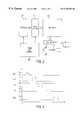
- FIG. 1shows a simplified circuit for a pixel of an exemplary CMOS imager using a photogate and having a pixel photodetector circuit 14 and a readout circuit 60 .
- FIG. 1shows the circuitry for operation of a single pixel, that in practical use there will be an M ⁇ N array of pixels arranged in rows and columns with the pixels of the array accessed using row and column select circuitry, as described in more detail below.
- the photodetector circuit 14is shown in part as a cross-sectional view of a semiconductor substrate 16 typically a p-type silicon, having a surface well of p-type material 20 .
- An optional layer 18 of p-type materialmay be used if desired, but is not required.
- Substrate 16may be formed of; for example, Si, SiGe, Ge, or GC.
- the entire substrate 16is p-type doped silicon substrate and may contain a surface p-well 20 (with layer 18 omitted), but many other options are possible, such as, for example p on p ⁇ substrates, p on p+ substrates, p-wells in n-type substrates or the like.
- wafer or substrate used in the descriptionincludes any semiconductor-based structure having an exposed surface in which to form the circuit structure used in the invention.
- Wafer and substrateare to be understood as including silicon-on-insulator (SOI) technology, silicon-on-sapphire (SOS) technology, doped and undoped semiconductors, epitaxial layers of silicon supported by a base semiconductor foundation, and other semiconductor structures.
- SOIsilicon-on-insulator
- SOSsilicon-on-sapphire
- doped and undoped semiconductorssilicon-on-insulator
- epitaxial layers of silicon supported by a base semiconductor foundationand other semiconductor structures.
- previous process stepsmay have been utilized to form regions/junctions in the base semiconductor structure or foundation.
- An insulating layer 22such as, for example, silicon dioxide is formed on the upper surface of p-well 20 .
- the p-type layermay be a p-well formed in substrate 16 .
- a photogate 24thin enough to pass radiant energy or of a material which passes radiant energy is formed on the insulating layer 22 .
- the photogate 24receives an applied control signal PG which causes the initial accumulation of pixel charges in n+ region 26 .
- the n+ type region 26adjacent one side of photogate 24 , is formed in the upper surface of p-well 20 .
- a transfer gate 28is formed on insulating layer 22 between n+ type region 26 and a second n+ type region 30 formed in p-well 20 .
- the n+ regions 26 and 30 and transfer gate 28form a charge transfer transistor 29 which is controlled by a transfer signal TX.
- the n+ region 30is typically called a floating diffusion region. It is also a node for passing charge accumulated thereat to the gate of a source follower transistor 36 described below.
- a reset gate 32is also formed on insulating layer 22 adjacent and between n+ type region 30 and another n+ region 34 which is also formed in p-well 20 .
- the reset gate 32 and n+ regions 30 and 34form a reset transistor 31 which is controlled by a reset signal RST.
- the n+ type region 34is coupled to voltage source V DD , e.g., 5 volts.
- the transfer and reset transistors 29 , 31are n-channel transistors as described in this implementation of a CMOS imager circuit in a p-well. It should be understood that it is possible to implement a CMOS imager in an n-well in which case each of the transistors would be p-channel transistors. It should also be noted that while FIG. 1 shows the use of a transfer gate 28 and associated transistor 29 , this structure provides advantages, but is not required.
- Photodetector circuit 14also includes two additional n-channel transistors, source follower transistor 36 and row select transistor 38 .
- Transistors 36 , 38arc coupled in series, source to drain, with the source of transistor 36 also coupled over lead 40 to voltage source V DD and the drain of transistor 38 coupled to a lead 42 .
- the drain of row select transistor 38is connected via conductor 42 to the drains of similar row select transistors for other pixels in a given pixel row.
- a load transistor 39is also coupled between the drain of transistor 38 and a voltage source V SS , e.g. 0 volts.
- Transistor 39is kept on by a signal V I,N applied to its gate.
- the imagerincludes a readout circuit 60 which includes a signal sample and hold (S/H) circuit including a S/H n-channel field effect transistor 62 and a signal storage capacitor 64 connected to the source follower transistor 36 through row transistor 38 .
- the other side of the capacitor 64is connected to a source voltage V SS .
- the upper side of the capacitor 64is also connected to the gate of a p-channel output transistor 66 .
- the drain of the output transistor 66is connected through a column select transistor 68 to a signal sample output node V OUTS and through a load transistor 70 to the voltage supply V DD .
- a signal called “signal sample and hold” (SHS)briefly turns on the S/H transistor 62 after the charge accumulated beneath the photogate electrode 24 has been transferred to the floating diffusion node 30 and from there to the source follower transistor 36 and through row select transistor 38 to line 42 , so that the capacitor 64 stores a voltage representing the amount of charge previously accumulated beneath the photogate electrode 24 .
- SHSsignal sample and hold
- the readout circuit 60also includes a reset sample and hold (S/H) circuit including a S/H transistor 72 and a signal storage capacitor 74 connected through the S/H transistor 72 and through the row select transistor 38 to the source of the source follower transistor 36 .
- the other side of the capacitor 74is connected to the source voltage V SS .
- the upper side of the capacitor 74is also connected to the gate of a p-channel output transistor 76 .
- the drain of the output transistor 76is connected through a p-channel column select transistor 78 to a reset sample output node V OUTR and through a load transistor 80 to the supply voltage V DD .
- a signal called “reset sample and hold” (SHR)briefly turns on the S/H transistor 72 immediately after the reset signal RST has caused reset transistor 31 to turn on and reset the potential of the floating diffusion node 30 , so that the capacitor 74 stores the voltage to which the floating diffusion node 30 has been reset.
- the readout circuit 60provides correlated sampling of the potential of the floating diffusion node 30 , first of the reset charge applied to node 30 by reset transistor 31 and then of the stored charge from the photogate 24 .
- the two samplings of the diffusion node 30charges produce respective output voltages V OUTR and V OUTS of the readout circuit 60 .
- These voltagesare then subtracted (V OUTR ⁇ V OUTR ) by subtractor 82 to provide an output signal terminal 81 which is an image signal independent of pixel to pixel variations caused by fabrication variations in the reset voltage transistor 31 which might cause pixel to pixel variations in the output signal.
- FIG. 2illustrates a block diagram for a CMOS imager having a pixel array 200 with each pixel cell being constructed in the manner shown by element 14 of FIG. 1 .
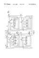
- FIG. 4shows a 2 ⁇ 2 portion of pixel array 200 .
- Pixel array 200comprises a plurality of pixels arranged in a predetermined number of columns and rows. The pixels of each row in array 200 are all turned on at the same time by a row select line, e.g., line 86 , and the pixels of each column are selectively output by a column select line, e.g., line 42 .
- a plurality of rows and column linesare provided for the entire array 200 .
- the row linesare selectively activated by the row driver 210 in response to row address decoder 220 and the column select lines are selectively activated by the column driver 260 in response to column address decoder 270 .
- a row and column addressis provided for each pixel.
- the CMOS imageris operated by the control circuit 250 which controls address decoders 220 , 270 for selecting the appropriate row and column lines for pixel readout, and row and column driver circuitry 210 , 260 which apply driving voltage to the drive transistors of the selected row and column lines.
- FIG. 3shows a simplified timing diagram for the signals used to transfer charge out of photodetector circuit 14 of the FIG. 1 CMOS imager.
- the photogate signal PGis nominally set to 5V and pulsed from 5V to 0V during integration.
- the reset signal RSTis nominally set at 2.5V.
- the RST voltagewhich is applied to the gate 32 of reset transistor 31 , causes transistor 31 to turn on and the floating diffusion node 30 to charge to the V DD ) voltage present at n+ region 34 (less the voltage drop V TH of transistor 31 ). This resets the floating diffusion node 30 to a predetermined voltage (V DD ⁇ V TH ).
- the charge on floating diffusion node 30is applied to the gate of the source follower transistor 36 to control the current passing through transistor 38 , which has been turned on by a row select (ROW) signal, and load transistor 39 .
- This currentis translated into a voltage on line 42 which is next sampled by providing a SHR signal to the S/H transistor 72 which charges capacitor 74 with the source follower transistor output voltage on line 42 representing the reset charge present at floating diffusion node 30 .
- the PG signalis next pulsed to 0 volts, causing charge to be collected in n+ region 26 .
- a transfer gate voltage TXis then applied to transfer gate 28 of transistor 29 to cause the charge in n+ region 26 to transfer to floating diffusion node 30 .
- the transfer gate voltage TXmay be pulsed or held to a fixed DC potential.
- the transfer gate voltage TXmust be pulsed.
- the new output voltage on line 42 generated by source follower transistor 36 currentis then sampled onto capacitor 64 by enabling the sample and hold switch 62 by signal SHS.
- the column select signalis next applied to transistors 68 and 70 and the respective charges stored in capacitors 64 and 74 are subtracted in subtractor 82 to provide a pixel output signal at terminal 81 .
- CMOS imagersmay dispense with the transfer gate 28 and associated transistor 29 , or retain these structures while biasing the transfer transistor 29 to an always “on” state.
- CMOS imagerThe operation of the charge collection of the CMOS imager is known in the art and is described in several publications such as Mendis et al., “Progress in CMOS Active Pixel Image Sensors,” SPIE Vol. 2172 , pp. 19-29 (1994); Mendis et al., “CMOS Active Pixel Image Sensors for Highly Integrated Imaging Systems,” IEEE Journal of Solid State Circuits, Vol. 32(2) (1997); and Eric R. Fossum, “CMOS Image Sensors: Electronic Camera on a Chip,” IEDM Vol. 95, pp. 17-25 (1995) as well as other publications. These references are incorporated herein by reference.
- the pixel cell 14 shown in FIG. 1contains a transfer transistor 29 having a gate stack 28 , a source n+ region 26 and a drain floating diffusion region 30 . Because the transfer gate stack 28 is separated from the photogate 24 by a relatively wide gap, e.g., 0.25 microns, the presence of a coupling region 26 is necessary to electrically couple the photogate 24 to the transfer gate stack 28 . When a signal TX is applied to the transfer gate stack 28 , the coupling region 26 functions as a conducting channel to pass charges from the doped layer 27 under the photogate into the channel region of the transfer transistor 29 , and then to the floating diffusion region 30 .
- this pixel cell 14is simple to fabricate because it is a single polysilicon process, i.e., it uses a single layer of polysilicon as the gate layer in the photogate 24 , transfer gate 28 and reset gate 32 , it has the disadvantages of added noise and incomplete charge transfer as a result of having to incorporate the diffused region 26 .
- double polysilicon structureshave been developed in which the photogate 24 and reset gate 32 are formed using the same layer of polysilicon. After spacer formation the top surface of all polysilicon gates are then oxidized, and then a transfer gate 28 is formed from a second layer of polysilicon that overlaps the photogate 24 to some degree. The overlapping of the photogate 24 and the transfer gate 28 with only a thin, e.g., less than 100 nm, layer of spacer insulator between them permits electrical coupling to occur between the doped layer 27 underlying the photogate 24 and the floating diffusion region 30 . No coupling region 26 is required for this pixel cell 14 .
- this pixel cell 14provides improved control over the potential stored in the 100 nm overlapping region between the edge of the photogate 24 and the transfer gate 28 , and results in increased charge transfer from the doped layer 27 to the floating diffusion region 30 , there are significant processing difficulties in the fabrication methods used to create the pixel cell 14 .
- the oxidation of the photogate stack 24 prior to transfer gate stack 28 formationresults in asperities, points, and other defects in the oxide layer insulating the transfer gate polysilicon from the photogate polysilicon, resulting in low breakdown of the insulating gate oxide between these two overlying polysilicons, improper electrical functioning, and poor processing yield.
- this oxidation of the first poly,silicon layer, prior to the deposition of the second polysilicon layer which will form the transfer gate 28forms the second gate oxide under the transfer gate.
- the gate oxidemust be grown thinner maintain low threshold voltages and maintain performance at the shorter geometries. So the thinning of the second gate oxide continues to cause a degradation in the breakdown voltage between these two overlapping polysilicon layers.
- This processalso suffers from the alignment required to do the masked implant of the n-doped region 27 , requiring careful alignment so that the doped region 27 does not extend across the transfer gate 28 which will be formed in later processing. In order to achieve this the transfer gate 28 is made larger to account for implant misalignment errors.
- This processalso suffers from the fact that all transistors formed by the first polysilicon deposition including the photogate 24 and reset gate 32 cannot be silicide gates, which would improve circuit speed and performance, because of two reasons: (1) the top silicide cannot be oxidized to provide a reliable insulating oxide between the photogate 24 and the transfer gate 28 and (2) a silicide layer on top of the photogate would block signal light from passing through the photogate into the signal storage region 27 below the photogate.
- an improved multi-layered gate structureformed with an overlapping second gate so that a doped region is not required to transfer charge between the two gates.
- a multi-layered transfer gate 28 and an overlapping photogate 24or a multi-layered photogate 24 with an overlapping transfer gate 28 so that a n-doped region 26 is not required.
- a method of fabricating a multi-layered gatethat solves the reduced process yield associated with the low photogate polysilicon to transfer polysilicon breakdown voltage is needed. It would also be advantageous if this new method would also provide silicided gates for improved speed and circuit performance while simultaneously allowing signal light to pass through the photogate.
- the present inventionprovides a multi-layered gate stack process for use in fabricating a pixel sensor cell.
- the multi-layered gateshave multiple layers including a conductive laver, an optional silicide layer, and an insulating layer, all of which are patterned and etched simultaneously over a first insulating layer. Also provided are methods for forming the multi-layered gates of the present invention, and a process that achieves high yield overlap process for a photogate—transfer gate overlap that does not require the n-doped region 26 .
- the combination of a multi-layered gate and an overlapping gatemay be a multi-layered transfer gate with an overlapping photogate, a multi-layered photogate with an overlapping transfer gate, a multi-layered source follower gate with an overlapping row select gate, a multi-layered row select gate with an overlapping source follower gate, or any other suitable combination.
- FIG. 1is a representative circuit of a CMOS imager.
- FIG. 2is a block diagram of a CMOS pixel sensor chip.
- FIG. 3is a representative timing diagram for the CMOS imager.
- FIG. 4is a representative pixel layout showing a 2 ⁇ 2 pixel layout.
- FIG. 5is a cross-sectional view of a pixel sensor cell according to one embodiment of the present invention.
- FIG. 6is a cross-sectional view of a pixel sensor cell according to a second embodiment of the present invention.
- FIG. 7is a cross-sectional view of a pixel sensor cell according to a third embodiment of the present invention.
- FIG. 8is a cross-sectional view of a pixel sensor cell according to a fourth embodiment of the present invention.
- FIG. 9is a cross-sectional view of a semiconductor wafer undergoing the process of a preferred embodiment of the invention.
- FIG. 10shows the wafer of FIG. 9 at a processing step subsequent to that shown in FIG. 9 .
- FIG. 11shows the wafer of FIG. 9 at a processing step subsequent to that shown in FIG. 10 .
- FIG. 12shows the wafer of FIG. 9 at a processing step subsequent to that shown in FIG. 11 .
- FIG. 13shows the wafer of FIG. 9 at a processing step subsequent to that shown in FIG. 12 .
- FIG. 14shows the wafer of FIG. 9 at a processing step subsequent to that shown in FIG. 13 .
- FIG. 15shows the wafer of FIG. 9 at a processing step subsequent to that shown in FIG. 14 .
- FIG. 16shows the wafer of FIG. 9 at a processing step subsequent to that shown in FIG. 15 .
- FIG. 17shows the wafer of FIG. 9 at a processing step subsequent to that shown in FIG. 16 .
- FIG. 18shows the wafer of FIG. 9 at a processing step subsequent to that shown in FIG. 17 .
- FIG. 19is an illustration of a computer system having a CMOS imager according to the present invention.
- wafer and substrateare to be understood as including silicon-on-insulator (SOI) or silicon-on-sapphire (SOS) technology, doped and undoped semiconductors, epitaxial layers of silicon supported by a base semiconductor foundation, and other semiconductor structures.
- SOIsilicon-on-insulator
- SOSsilicon-on-sapphire
- doped and undoped semiconductorsepitaxial layers of silicon supported by a base semiconductor foundation
- previous process stepsmay have been utilized to form regions or junctions in the base semiconductor structure or foundation.
- the semiconductorneed not be silicon-based, but could be based on silicon-germanium, germanium, or gallium arsenide.
- pixelrefers to a picture element unit cell containing a photosensor and transistors for converting electromagnetic radiation to an electrical signal.
- a representative pixelis illustrated in the figures and description herein, and typically fabrication of all pixels in an imager will proceed simultaneously in a similar fashion.
- the following detailed descriptionis, therefore, not to be taken in a limiting sense, and the scope of the present invention is defined by the appended claims.
- the structure of the pixel cell 14 of the first embodimentis shown in more detail in FIG. 5 .
- the pixel cell 14may be formed in a substrate 16 having a doped layer or well 20 of a first conductivity type, which for exemplary purposes is treated as a p-type substrate.
- Three gate stacksare formed in the pixel cell 14 as shown: a multi-layered transfer gate stack 28 , a multi-layered reset transistor gate stack 32 of the reset transistor 31 , and a semitransparent photogate conductor 24 formed partially over the multi-layered transfer gate stack 28 .
- a doped region 30that is the source for the reset transistor 31
- a doped region 34that acts as a drain for the reset transistor.
- the doped regions 30 , 34are doped to a second conductivity type, which for exemplary purposes is treated as n-type.
- the first doped region 30is the floating diffusion region, sometimes also referred to as a floating diffusion node, and the second doped region 34 is connected to voltage source Vdd.
- the multi-layered transfer gate stack 28 and the multi-layered reset gate stack 32include a first insulating layer 100 of grown or deposited silicon oxide on the doped laver 20 , and a conductive layer 102 , such as doped polysilicon or other suitable material, over the first insulating layer 100 .
- a second insulating layer 108 of, for example, silicon oxide (silicon dioxide), nitride (silicon nitride), oxynitride (silicon oxynitride), ON (oxide-nitride), NO (nitride-oxide), or ONO (oxide-nitride-oxide)may be formed, if desired; also a silicide layer 106 may be formed in the multi-layered gate stacks 28 , 32 , between the conductive layer 102 and the second insulating layer 108 , if desired.
- all other transistors in the imager circuit design, except for the photogatemay have this additionally formed silicide layer, thus improving gate delay and increasing circuit speed.
- This silicide layermay be titanium silicide, tungsten silicide, cobalt silicide, molybdenum silicide, or tantalum silicide.
- Layer 106could also be a barrier layer/refractory metal such as TiN/W or WN X /W or is it could be entirely formed of WN X .
- the implanted n-doped region 27is self-aligned to the transfer gate edge and forms a photosensitive charge storage region for collecting photogenerated electrons.
- Insulating sidewalls 110 of, for example, silicon dioxide, silicon nitride, silicon oxynitride, ON, NO, or ONOare also formed on the sides of the gate stacks 28 , 32 .
- the photogate stack 24includes a first insulating laver 114 formed over the n-doped layer 27 , and a conductive layer 103 of doped polysilicon, tin oxide, indium tin oxide, or other suitable semitransparent conductive material over the first insulating layer 114 .
- the so-formed photogate 24is isolated from the multi-layered transfer gate stack 28 by the combination of the spacers 110 and the second insulating layer 108 .
- These layerscan be made relatively thick without sacrificing imager or circuit performance and thus achieve good isolation between the photogate and the transfer gate, high breakdown voltages, and high yield.
- This new processing methoddoes not depend on the non-uniform growth of an oxide on a polysilicon layer to provide isolation between two gates.
- the transfer gate stack 28has a second insulating layer 108 , and the conductive 106 and silicide 108 layers of the transfer gate stack 28 are isolated on the sides by sidewall spacers 110 , there is so-formed a uniformly thick isolation free of asperities and points that enables high breakdown voltages and high yield.
- the relative thickness and smoothness of the isolating insulators 108 , 110enables the formation thereon of a substantially defect-free gate layer 103 of the photogate 24 . Because the structural quality of the insulating layers 108 , 110 and the gate layer 103 is improved over structures known in the art, there are fewer electrical defects in photogate to transfer gate isolation of the present invention, and processing yields are improved.
- the edge of the photogate conductive layer 103is self-aligned to the edge of the transfer gate 28 so that no intervening doped region 26 is required as has been the case with past single polysilicon processes.
- the first gate oxide 100is grown just before depositing the first conductive layer 102 and the second gate oxide 114 is grown just before depositing a second conductive layer 103 which is, in the case of FIG. 5, a semitransparent layer that forms the photogate.
- the semitransparent photogate 24As light radiation 12 in the form of photons passes through the semitransparent photogate 24 , electron-hole pairs are created in the underlying silicon substrate and electrical carriers are stored in the doped layer 27 underneath the photogate 24 .
- the carriersmay be either electrons or holes, depending on the types of devices used in the pixel sensor cell 14 .
- the stored carriersare electrons.
- the transfer gateWhen a signal TX is applied to the conductive layer 106 of the transfer gate stack 28 , the transfer gate is turned on and electrical coupling occurs due to the narrow gap between the photogate 24 and the transfer gate stack 28 , and the coupling capacitance and electrical fringing fields between these two devices, and carriers are transferred from the doped layer 27 under the photogate into the floating diffusion region 30 .
- a multi-layered photogate 24 with an overlapping transfer gate 28works in essentially the same fashion as is described above for the multi-layered transfer gate 28 with an overlapping photogate 24 .
- the design of the gatesis varied as necessary to achieve proper electrical functioning of the device, for example, the multi-layered photogate 24 of FIG. 6 would not have the optional silicide layer 106 .
- the overlapping transfer gate in FIG. 6could have a silicide or barrier metal/refractory metal layer over the polysilicon layer 103 . Similar to FIG. 5, the first gate oxide 100 is grown just before depositing the first conductive layer 102 , and the second gate oxide 114 is grown just before depositing the second conductive layer 103 which is, in the case of FIG. 6, the transfer gate.
- FIGS. 7 and 8depict, respectively, a multi-layered row select gate 38 with an overlapping source follower gate 36 , and a multi-layered source follower gate 36 with an overlapping row select gate 38 .
- Charge on the floating diffusion region 30is connected to the source follower gate 36 via lead 44 . This charge regulates the degree to which the source follower transistor is turned on.
- the row select gate 38is also turned on by signal ROW, then current flows between source region 120 and drain region 122 , and via lead 42 to signal processing circuitry located outside the pixel array.
- the overlapping gatemay have a silicide or barrier/refractory metal layer over the polysilicon layer 103 and may also have an overlapping insulating layer.
- the multi-layered transfer gate 28is manufactured through a process described as follows, and illustrated by FIGS. 9 through 18.
- a substrate 16which may be any of the types of substrates described above, is doped to form a doped substrate layer or well 20 of a first conductivity type, which for exemplary purposes will be described as p-type.
- the process sequence described and illustrated belowprovides for the formation of n-channel devices in a p-type substrate. It follows that the invention may also be carried out by forming p-channel devices in an n-type substrate by substitution of the appropriately doped materials and addition of appropriate masks. Also, p-channel and n-channel devices may be formed in the same substrate.
- a multi-layered transfer gate with an overlapping photogateis described and illustrated herein, but the process of the present invention is not limited thereto. Fabrication of the other embodiments of the present invention such as a multi-layered row select gate with an overlapping source follower gate would proceed substantially as described below.
- FIG. 9The processing is shown in FIG. 9 after the field oxide isolation is completed.
- Field isolationis used to isolate doped or conductive regions to be later formed in the silicon substrate.
- Field oxidation by the LOCOS processwhich involves a thermal oxidation of the silicon is shown.
- STIshallow trench isolation
- the next stepis to form a first insulating layer 100 of silicon oxide, silicon nitride, silicon oxynitride, ON, NO, or ONO, on the top of the doped layer 20 by suitable means such as growth by thermal oxidation of the doped layer 20 , or by deposition.
- a first conductive layer 102is formed, by chemical vapor deposition (CVD), or other suitable means, on top of the first insulating layer 100 .
- the first conductive layer 102may be doped polysilicon and is preferably about 10 to 500 nm thick.
- a metal layer 104is formed on top of the first conductive layer 102 by suitable means such as CVD, evaporation, or sputtering.
- a silicide layer 106is formed by annealing the metal layer 104 at a temperature within the approximate range of 300 to 900 degrees Celsius.
- a second embodimentis to deposit the silicide layer 106 directly onto the first conductive layer 102 by CVD or other suitable means.
- the metal silicidemay be any suitable metal silicide such as the silicides of tungsten, titanium, molybdenum, tantalum, platinum, palladium, iridium or cobalt.
- the metal layercould be a deposited barrier metal/metal conductor laver combination such as TiN/W, WN X /W, or any other suitable barrier metal/metal conductor combination such as WN X alone, and it may be deposited by CVD, evaporation, or sputtering.
- FIG. 14depicts the next step in the process, in which a second insulating layer 108 is formed on the silicide layer 106 by CVD, or other suitable means.
- the second insulating layermay be formed from any suitable material such as silicon oxide, silicon nitride, ONO, ON, or NO. It is to be understood that the oxide layers could also be a silicum rich oxide layer commonly used as an inorganic ARC layer (anti-reflection coating), which additionally improves photo patterning.
- the next stepis to define gate stacks.
- a resist (not shown) and mask (not shown)are applied, and photolithographic techniques are used to define the areas which will be gate stacks across the wafer.
- a suitable removal processsuch as RIE or other directional etching is used to remove the second insulating layer 108 , the silicide layer 106 , and the first conductive layer 102 to leave a transfer gate stack 28 , a reset transistor gate stack 32 , and the first insulating layer 100 on the surface of the wafer.
- the first insulating layer 100may also be partially removed from the surface of the wafer in the regions exposed to the etch.
- Other transistors in the imaging pixelsuch as the source follower transistor and the row select transistor are similarly formed though not shown at this time. Also any peripheral logic transistors can be advantageously so formed at this point in the processing.
- spacers or sidewalls 110are formed on the sides of the gate stacks 28 , 32 .
- the sidewalls 110may be formed of deposited insulation materials such as silicon oxide, silicon nitride, silicon oxynitride, or ONO or ON or NO. After deposition of the insulating material it is etched using an anisotropic dry etch that forms the sidewall spacers. This anisotropic etch may partially or completely remove the remaining first insulating layer 100 .
- FIG. 16shows the gate oxide 100 to be completely removed by the spacer overetch in the regions where the gate oxide is not protected by the overlapping gate stack.
- the masked source-drain implant 34As shown in FIG. 17, after the spacers are formed, the masked source-drain implant 34 , the masked floating diffusion implant 30 , and the self-aligned masked photogate implant 27 are performed.
- these are all n-type implantssuch as arsenic, antimony, or phosphorus. It is possible with some sacrifice in performance to save costs by implanting these regions with just one or two masks rather than the three indicated herein.
- the implantsdiffuse under subsequent thermal treatment. In FIG. 17 we show these diffused, implanted regions after those thermal steps have occurred. There will be other masked implantations to improve transistor performance, set Vt's, etc., which for sake of simplicity, are not shown.
- the next stepis to form the photogate 24 .
- a second insulating laver 114is formed or reformed on the silicon substrate by suitable means such as growth by thermal oxidation.
- a second conductive layer 103is deposited, by CVD, or other suitable means, on top of the second insulating layer 114 .
- the second conductive layer 103may be doped polysilicon or other suitable semitransparent conductive material such as tin oxide or indium tin oxide, and is preferably about 10 to 500 nm thick.
- a resist (not shown) and mask (not shown)are applied to selectively pattern an area where the photogate 24 is to be formed.
- FIG. 18show the reset, transfer, and photogates in the imager after the photogate has been patterned, etched and the resist patterning layers removed.
- the multi-layered gate process with overlapping gatesis essentially complete at this stage, and conventional processing methods may then be used to form contacts and wiring to connect gate lines and other connections in the pixel cell 14 .
- the entire surfacemay then be covered with a passivation layer of, e.g., silicon dioxide, BSG, PSG, or BPSG, which is CMP planarized and etched to provide contact holes, which are then metallized to provide contacts to the photogate, reset gate, and transfer gate.
- Conventional multiple layers of conductors and insulatorsmay also be used to interconnect the structures in the manner shown in FIG. 1 .
- Pixel arrays having the transfer gates of the present invention, and described with reference to FIGS. 5-18,may be further processed as known in the art to arrive at CMOS imagers having the functions and features of those discussed with reference to FIGS. 1-4.
- a typical processor based system which includes a CMOS imager device according to the present inventionis illustrated generally at 400 in FIG. 19.
- a processor based systemis exemplary of a system having digital circuits which could include CMOS imager devices. Without being limiting, such a system could include a computer system, camera system, scanner, machine vision system, vehicle navigation system, video telephone, surveillance system, auto focus system, star tracker system, motion detection system, image stabilization system and data compression system for high-definition television, all of which can utilize the present invention.
- a processor systemsuch as a computer system for example generally comprises a central processing unit (CPU) 444 , e.g., a microprocessor, that communicates with an input/output (I/O) device 446 over a bus 452 .
- the CMOS imager 442also communicates with the system over bus 452 .
- the computer system 400also includes random access memory (RAM) 448 , and, in the case of a computer system may include peripheral devices such as a floppy disk drive 454 and a compact disk (CD) ROM drive 456 which also communicate with CPU 444 over the bus 452 .
- CMOS imager 442is preferably constructed as an integrated circuit which includes pixels containing a multi-layered gate, as previously described with respect to FIGS. 5 through 18.
- the CMOS imager 442may be combined with a processor, such as a CPU, digital signal processor or microprocessor, with or without memory storage, in a single integrated circuit, or may be on a different chip than the processor.
- the present inventionencompasses multi-layered gates in a pixel sensor cell that are at least partially overlapped by an adjacent gate.
- the multi-layered gateis a complete gate stack and exhibits improved insulation from the overlapping gate, thereby resulting in fewer shorts between the two gates.
- the process embodiments described hereinenable formation of a multi-layered gate with improved yield and reliability.
Landscapes
- Solid State Image Pick-Up Elements (AREA)
Abstract
Description
Claims (66)
Priority Applications (5)
| Application Number | Priority Date | Filing Date | Title |
|---|---|---|---|
| US09/333,011US6376868B1 (en) | 1999-06-15 | 1999-06-15 | Multi-layered gate for a CMOS imager |
| US09/686,944US6548352B1 (en) | 1999-06-15 | 2000-10-12 | Multi-layered gate for a CMOS imager |
| US09/832,856US6617623B2 (en) | 1999-06-15 | 2001-04-12 | Multi-layered gate for a CMOS imager |
| US10/341,368US6960795B2 (en) | 1999-06-15 | 2003-01-14 | Pixel sensor cell for use in an imaging device |
| US10/654,932US6835637B2 (en) | 1999-06-15 | 2003-09-05 | Multi-layered gate for a CMOS imager |
Applications Claiming Priority (1)
| Application Number | Priority Date | Filing Date | Title |
|---|---|---|---|
| US09/333,011US6376868B1 (en) | 1999-06-15 | 1999-06-15 | Multi-layered gate for a CMOS imager |
Related Child Applications (2)
| Application Number | Title | Priority Date | Filing Date |
|---|---|---|---|
| US09/686,944DivisionUS6548352B1 (en) | 1999-06-15 | 2000-10-12 | Multi-layered gate for a CMOS imager |
| US09/832,856DivisionUS6617623B2 (en) | 1999-06-15 | 2001-04-12 | Multi-layered gate for a CMOS imager |
Publications (1)
| Publication Number | Publication Date |
|---|---|
| US6376868B1true US6376868B1 (en) | 2002-04-23 |
Family
ID=23300870
Family Applications (5)
| Application Number | Title | Priority Date | Filing Date |
|---|---|---|---|
| US09/333,011Expired - LifetimeUS6376868B1 (en) | 1999-06-15 | 1999-06-15 | Multi-layered gate for a CMOS imager |
| US09/686,944Expired - LifetimeUS6548352B1 (en) | 1999-06-15 | 2000-10-12 | Multi-layered gate for a CMOS imager |
| US09/832,856Expired - LifetimeUS6617623B2 (en) | 1999-06-15 | 2001-04-12 | Multi-layered gate for a CMOS imager |
| US10/341,368Expired - LifetimeUS6960795B2 (en) | 1999-06-15 | 2003-01-14 | Pixel sensor cell for use in an imaging device |
| US10/654,932Expired - LifetimeUS6835637B2 (en) | 1999-06-15 | 2003-09-05 | Multi-layered gate for a CMOS imager |
Family Applications After (4)
| Application Number | Title | Priority Date | Filing Date |
|---|---|---|---|
| US09/686,944Expired - LifetimeUS6548352B1 (en) | 1999-06-15 | 2000-10-12 | Multi-layered gate for a CMOS imager |
| US09/832,856Expired - LifetimeUS6617623B2 (en) | 1999-06-15 | 2001-04-12 | Multi-layered gate for a CMOS imager |
| US10/341,368Expired - LifetimeUS6960795B2 (en) | 1999-06-15 | 2003-01-14 | Pixel sensor cell for use in an imaging device |
| US10/654,932Expired - LifetimeUS6835637B2 (en) | 1999-06-15 | 2003-09-05 | Multi-layered gate for a CMOS imager |
Country Status (1)
| Country | Link |
|---|---|
| US (5) | US6376868B1 (en) |
Cited By (129)
| Publication number | Priority date | Publication date | Assignee | Title |
|---|---|---|---|---|
| US20020168473A1 (en)* | 2001-05-08 | 2002-11-14 | Degussa Ag | Antimicrobial treatment of porous materials |
| US20030122169A1 (en)* | 1999-12-28 | 2003-07-03 | Jin-Su Han | Image sensor incorporating therein a capacitor structure and method for the manufacture thereof |
| US20030210439A1 (en)* | 2002-05-13 | 2003-11-13 | Atif Sarwari | Data download to imager chip using image sensor as a receptor |
| US20030228736A1 (en)* | 2002-06-10 | 2003-12-11 | Mitsubishi Denki Kabushiki Kaisha | Semiconductor device and manufacturing method thereof |
| US6774442B2 (en)* | 2000-07-21 | 2004-08-10 | Renesas Technology Corp. | Semiconductor device and CMOS transistor |
| WO2004075299A1 (en) | 2003-02-19 | 2004-09-02 | Micron Technology, Inc. | Cmos image sensor and method of fabrication |
| US20040251394A1 (en)* | 2003-06-11 | 2004-12-16 | Rhodes Howard E. | Dual conversion gain imagers |
| US20040251482A1 (en)* | 2003-06-16 | 2004-12-16 | Rhodes Howard E. | Method and apparatus for reducing imager floating diffusion leakage |
| US20040262646A1 (en)* | 2003-06-16 | 2004-12-30 | Inna Patrick | Pixel design to maximize photodiode capacitance and method of forming same |
| KR100464949B1 (en)* | 2000-08-31 | 2005-01-05 | 매그나칩 반도체 유한회사 | Method for forming image sensor capable of improving characteristics of photodiode |
| US20050001277A1 (en)* | 2003-07-03 | 2005-01-06 | Rhodes Howard E. | Optimized transistor for imager device |
| US20050001143A1 (en)* | 2003-07-02 | 2005-01-06 | Rhodes Howard E. | CMOS imaging for ALC and CDS |
| US20050042793A1 (en)* | 2003-06-25 | 2005-02-24 | Chandra Mouli | Reduced barrier photodiode/gate device structure for high efficiency charge transfer and reduced lag and method of formation |
| US20050041128A1 (en)* | 2003-08-22 | 2005-02-24 | Baker R. Jacob | Per column one-bit ADC for image sensors |
| US20050051701A1 (en)* | 2003-09-05 | 2005-03-10 | Hong Sungkwon C. | Image sensor having pinned floating diffusion diode |
| US20050051702A1 (en)* | 2003-09-08 | 2005-03-10 | Hong Sungkwon Chris | Image sensor with photo diode gate |
| US20050057680A1 (en)* | 2003-09-16 | 2005-03-17 | Agan Martin J. | Method and apparatus for controlling integration time in imagers |
| US20050064665A1 (en)* | 2003-09-23 | 2005-03-24 | Han Chang Hun | Method for manufacturing a CMOS image sensor |
| US20050062068A1 (en)* | 2001-09-17 | 2005-03-24 | Sony Corporation | Solid-state imaging device and method for manufacturing same |
| US6879340B1 (en) | 1998-08-19 | 2005-04-12 | Micron Technology Inc. | CMOS imager with integrated non-volatile memory |
| US20050082461A1 (en)* | 2003-10-15 | 2005-04-21 | Bock Nikolai E. | Pixel with differential readout |
| US20050082582A1 (en)* | 2003-10-21 | 2005-04-21 | Rhodes Howard E. | Single poly CMOS imager |
| US6900121B1 (en)* | 2002-03-14 | 2005-05-31 | Advanced Micro Devices, Inc. | Laser thermal annealing to eliminate oxide voiding |
| US20050128596A1 (en)* | 2003-10-09 | 2005-06-16 | Jin Li | Method for balancing color response of imagers |
| US20050191814A1 (en)* | 2004-02-26 | 2005-09-01 | Mcclure Brent A. | Method of forming a contact in a pixel cell |
| US20050196890A1 (en)* | 2003-10-09 | 2005-09-08 | Chandra Mouli | Ultra-shallow photodiode using indium |
| US20050205904A1 (en)* | 2003-05-23 | 2005-09-22 | Sungkwon Hong | Method of forming an elevated photodiode in an image sensor |
| US20050205761A1 (en)* | 2004-03-22 | 2005-09-22 | Joey Shah | Pixel with multiple readout circuits |
| US20050243193A1 (en)* | 2004-04-30 | 2005-11-03 | Bob Gove | Suppression of row-wise noise in an imager |
| US20050247896A1 (en)* | 2004-05-06 | 2005-11-10 | Caldwell John L | Method and apparatus for imager die package quality testing |
| US20050274994A1 (en)* | 2004-06-14 | 2005-12-15 | Rhodes Howard E | High dielectric constant spacer for imagers |
| US20050280012A1 (en)* | 2003-10-09 | 2005-12-22 | Micron Technology, Inc. | Gapless microlens array and method of fabrication |
| US20060001060A1 (en)* | 2004-07-01 | 2006-01-05 | Rhodes Howard E | Pixel cell with a controlled output signal knee characteristic response |
| US20060007337A1 (en)* | 2004-07-12 | 2006-01-12 | Roger Panicacci | Dual panel pixel readout in an imager |
| US20060007329A1 (en)* | 2004-07-12 | 2006-01-12 | Roger Panicacci | Column-wise clamp voltage driver for suppression of noise in an imager |
| US20060006915A1 (en)* | 2004-07-12 | 2006-01-12 | Hai Yan | Signal slew rate control for image sensors |
| US20060011955A1 (en)* | 2004-07-19 | 2006-01-19 | Baggenstoss William J | Pixel cell having a grated interface |
| US20060027887A1 (en)* | 2003-10-09 | 2006-02-09 | Micron Technology, Inc. | Gapless microlens array and method of fabrication |
| US20060033129A1 (en)* | 2004-08-16 | 2006-02-16 | Chandra Mouli | Low dark current image sensors with epitaxial SiC and/or carbonated channels for array transistors |
| US20060038207A1 (en)* | 2004-08-19 | 2006-02-23 | Hong Sungkwon C | Wide dynamic range sensor having a pinned diode with multiple pinned voltages |
| US20060044431A1 (en)* | 2004-08-27 | 2006-03-02 | Ilia Ovsiannikov | Apparatus and method for processing images |
| US20060060904A1 (en)* | 2003-11-18 | 2006-03-23 | Hong Sungkwon C | Dual gate structure for imagers and method of formation |
| EP1420454A3 (en)* | 2002-11-13 | 2006-04-05 | Eastman Kodak Company | A method for creating a double transparent electrode pseudo two-phase ccd |
| US20060081395A1 (en)* | 2004-10-08 | 2006-04-20 | Hitachi, Ltd. | Cover unit for fuel tank |
| US20060104564A1 (en)* | 2004-11-15 | 2006-05-18 | Catrysse Peter B | Integrated waveguide and method for designing integrated waveguide |
| US20060119720A1 (en)* | 2004-12-03 | 2006-06-08 | Micron Technology, Inc. | Imager pixel with capacitance circuit for boosting reset voltage |
| US20060151848A1 (en)* | 1999-06-18 | 2006-07-13 | Rhodes Howard E | Photogate with improved short wavelength response for a CMOS imager |
| US20060152601A1 (en)* | 2005-01-13 | 2006-07-13 | Micron Technology, Inc. | Low cost digital camera with one-time programmable memory |
| US20060180741A1 (en)* | 2005-02-11 | 2006-08-17 | Micron Technology, Inc. | Method and apparatus for dark current and hot pixel reduction in active pixel image sensors |
| US20060187329A1 (en)* | 2005-02-24 | 2006-08-24 | Micron Technology, Inc. | Clamped capacitor readout noise rejection circuit for imagers |
| US20060192864A1 (en)* | 2005-02-28 | 2006-08-31 | Rick Mauritzson | Imager row-wise noise correction |
| US20060214085A1 (en)* | 2005-03-24 | 2006-09-28 | Micron Technology, Inc. | Readout technique for increasing or maintaining dynamic range in image sensors |
| US20060231875A1 (en)* | 2005-04-15 | 2006-10-19 | Micron Technology, Inc. | Dual conversion gain pixel using Schottky and ohmic contacts to the floating diffusion region and methods of fabrication and operation |
| US20060238634A1 (en)* | 2005-04-21 | 2006-10-26 | Micron Technology, Inc. | Apparatus and method for providing anti-eclipse operation for imaging sensors |
| US20060249654A1 (en)* | 2005-05-06 | 2006-11-09 | Silsby Christopher D | Pixel with spatially varying sensor positions |
| US20060249653A1 (en)* | 2005-05-06 | 2006-11-09 | Gazeley William G | Pixel with spatially varying metal route positions |
| US20060255381A1 (en)* | 2005-05-10 | 2006-11-16 | Micron Technology, Inc. | Pixel with gate contacts over active region and method of forming same |
| US20060261385A1 (en)* | 2005-05-23 | 2006-11-23 | Micron Technology, Inc. | Phase shift transparent structures for imaging devices |
| US20060261342A1 (en)* | 2005-05-19 | 2006-11-23 | Micron Technology, Inc. | Imaging device having a pixel cell with a transparent conductive interconnect line and the method of making the pixel cell |
| US20060279649A1 (en)* | 2005-06-09 | 2006-12-14 | Cole Bryan G | Reduced imager crosstalk and pixel noise using extended buried contacts |
| US20060278809A1 (en)* | 2005-06-14 | 2006-12-14 | Micron Technology, Inc. | Pixel individual anti-eclipse circuit and its operation manner |
| US20060285000A1 (en)* | 2003-09-10 | 2006-12-21 | Keiji Mabuchi | Semiconductor device, and control method and device for driving unit component of semiconductor device |
| US20060292735A1 (en)* | 2003-10-09 | 2006-12-28 | Micron Technology, Inc. | Methods for creating gapless inner microlenses, arrays of microlenses, and imagers having same |
| US20070009248A1 (en)* | 2005-07-08 | 2007-01-11 | Micron Technology, Inc. | Method and apparatus for auto focusing an imaging device |
| US20070012917A1 (en)* | 2005-07-12 | 2007-01-18 | Micron Technology, Inc. | Pixel with transfer gate with no isolation edge |
| US20070012970A1 (en)* | 2005-07-12 | 2007-01-18 | Micron Technology, Inc. | Image sensor with SOI substrate |
| US20070031988A1 (en)* | 2005-08-03 | 2007-02-08 | Micron Technology, Inc. | Backside silicon wafer design reducing image artifacts from infrared radiation |
| US20070030379A1 (en)* | 2005-08-03 | 2007-02-08 | Micron Technology, Inc. | Circular symmetrical microlens/color filter array shift and digital lens shading correction |
| US20070035649A1 (en)* | 2005-08-10 | 2007-02-15 | Micron Technology, Inc. | Image pixel reset through dual conversion gain gate |
| US20070040102A1 (en)* | 2005-08-22 | 2007-02-22 | Micron Technology, Inc. | Method and apparatus providing an optical guide for an imager pixel having a ring of air-filled spaced slots around a photosensor |
| US20070045685A1 (en)* | 2005-08-24 | 2007-03-01 | Micron Technology, Inc. | Method and apparatus providing integrated color pixel with buried sub-wavelength gratings in solid state imagers |
| US20070045513A1 (en)* | 2005-08-30 | 2007-03-01 | Lee Ji S | Image sensors with optical trench |
| US20070045668A1 (en)* | 2005-08-26 | 2007-03-01 | Micron Technology, Inc. | Vertical anti-blooming control and cross-talk reduction for imagers |
| US20070108476A1 (en)* | 2004-06-01 | 2007-05-17 | Hong Sungkwon C | Imager with reflector mirrors |
| US20070120162A1 (en)* | 2005-11-30 | 2007-05-31 | Micron Technology, Inc. | Method and apparatus for blocking light to peripheral circuitry of an imager device |
| US20070133870A1 (en)* | 2005-12-14 | 2007-06-14 | Micron Technology, Inc. | Method, apparatus, and system for improved color statistic pruning for automatic color balance |
| WO2007066944A1 (en)* | 2005-12-05 | 2007-06-14 | Electronics And Telecommunications Research Institute | Low-noise image sensor and transistor for image sensor |
| US20070145512A1 (en)* | 2004-09-27 | 2007-06-28 | Rhodes Howard E | Photogate stack with nitride insulating cap over conductive layer |
| US20070158709A1 (en)* | 2006-01-09 | 2007-07-12 | Micron Technology, Inc. | Image sensor with improved surface depletion |
| US20070165123A1 (en)* | 2006-01-13 | 2007-07-19 | Micron Technology, Inc. | Method and apparatus providing pixel storage gate charge sensing for electronic stabilization in imagers |
| US20070182845A1 (en)* | 2006-02-03 | 2007-08-09 | Micron Technology, Inc. | Auto exposure for digital imagers |
| US20070187572A1 (en)* | 2006-02-15 | 2007-08-16 | Micron Technology, Inc. | Method and apparatus of determining the best focus position of a lens |
| US20070205354A1 (en)* | 2006-03-06 | 2007-09-06 | Micron Technology, Inc. | Image sensor light shield |
| US20070235631A1 (en)* | 2006-03-30 | 2007-10-11 | Micron Technology, Inc. | Reducing noise in an imager |
| US20070238034A1 (en)* | 2006-04-07 | 2007-10-11 | Micron Technology, Inc. | Color filter array and imaging device containing such color filter array and method of fabrication |
| US20070237888A1 (en)* | 2006-04-07 | 2007-10-11 | Micron Technology, Inc. | Methods to make sidewall light shields for color filter array |
| US20070241258A1 (en)* | 2006-04-12 | 2007-10-18 | Micron Technology, Inc. | Imaging device with reduced row readout time and method of operating the same |
| US20070284510A1 (en)* | 2006-06-09 | 2007-12-13 | Micron Technology, Inc. | Method and apparatus providing a microlens for an image sensor |
| US20080018762A1 (en)* | 2006-07-18 | 2008-01-24 | Micron Technology, Inc. | Method, apparatus and system for charge injection suppression in active pixel sensors |
| US20080023737A1 (en)* | 2006-07-24 | 2008-01-31 | Dongbu Hitek Co., Ltd. | Image sensor and method for manufacturing the same |
| US20080049126A1 (en)* | 2006-08-28 | 2008-02-28 | Micron Technology, Inc. | Color filter array and method of fabrication and use |
| US20080049133A1 (en)* | 2006-08-25 | 2008-02-28 | Micron Technology, Inc. | Method, apparatus, and system providing an imager with pixels having extended dynamic range |
| US20080054320A1 (en)* | 2006-08-31 | 2008-03-06 | Micron Technology, Inc. | Method, apparatus and system providing suppression of noise in a digital imager |
| US20080056704A1 (en)* | 2006-08-30 | 2008-03-06 | Ilia Ovsiannikov | Method, apparatus and system for dynamic range estimation of imaged scenes |
| US20080055128A1 (en)* | 2006-08-31 | 2008-03-06 | Micron Technology, Inc. | Method and apparatus for calibrating imaging device circuits |
| US20080054319A1 (en)* | 2006-08-31 | 2008-03-06 | Micron Technology, Inc. | Transparent-channel thin-film transistor-based pixels for high-performance image sensors |
| US20080061830A1 (en)* | 2006-08-24 | 2008-03-13 | Yan Lee | Method, apparatus, and system providing power supply independent imager output driver having a constant slew rate |
| US20080074523A1 (en)* | 2006-08-29 | 2008-03-27 | Micron Technology, Inc. | In-pixel analog memory with non-destructive read sense circuit for high dynamic range global shutter pixel operation |
| US20080074524A1 (en)* | 2006-08-29 | 2008-03-27 | Micron Technology, Inc. | Skimmed charge capture and charge packet removal for increased effective pixel photosensor full well capacity |
| US20080170228A1 (en)* | 2007-01-17 | 2008-07-17 | Micron Technology, Inc. | Method and apparatus for wafer level calibration of imaging sensors |
| US20080173793A1 (en)* | 2007-01-23 | 2008-07-24 | Micron Technology, Inc. | Method, apparatus and system providing holographic layer as micro-lens and color filter array in an imager |
| US20080204580A1 (en)* | 2007-02-28 | 2008-08-28 | Micron Technology, Inc. | Method, apparatus and system providing imaging device with color filter array |
| US20080239111A1 (en)* | 2007-03-26 | 2008-10-02 | Micron Technology, Inc. | Method and appratus for dark current compensation of imaging sensors |
| US20080259194A1 (en)* | 2007-04-23 | 2008-10-23 | Amnon Silverstein | Method, apparatus, and system providing a rectilinear pixel grid with radially scaled pixels |
| US20080277693A1 (en)* | 2007-05-10 | 2008-11-13 | Micron Technology, Inc. | Imager element, device and system with recessed transfer gate |
| US20080284879A1 (en)* | 2007-05-18 | 2008-11-20 | Micron Technology, Inc. | Methods and apparatuses for vignetting correction in image signals |
| US20080298708A1 (en)* | 2007-05-31 | 2008-12-04 | Micron Technology, Inc. | Methods and apparatuses that reduce noise in image signals |
| US20080309810A1 (en)* | 2007-06-15 | 2008-12-18 | Scott Smith | Images with high speed digital frame transfer and frame processing |
| US20080315263A1 (en)* | 2007-06-20 | 2008-12-25 | Micron Technology, Inc. | Imager pixel structure and circuit |
| US20090002539A1 (en)* | 2007-06-27 | 2009-01-01 | Roger Panicacci | Pixel to pixel charge copier circuit apparatus, systems, and methods |
| US20090040326A1 (en)* | 2007-08-09 | 2009-02-12 | Micron Technology, Inc | Methods and apparatuses for supplying current using a digital sequence |
| US20090053848A1 (en)* | 2007-08-23 | 2009-02-26 | Micron Technology, Inc. | Method and apparatus providing imager pixels with shared pixel components |
| US20090075465A1 (en)* | 2007-09-19 | 2009-03-19 | Xiaofeng Fan | Methods of forming a conductive interconnect in a pixel of an imager and in other integrated circuitry |
| US20090090844A1 (en)* | 2007-10-04 | 2009-04-09 | Micron Technology, Inc. | Biasing apparatus, systems, and methods |
| US20090097743A1 (en)* | 2007-10-16 | 2009-04-16 | Micron Technology, Inc. | Method and apparatus providing hardware-efficient demosaicing of image data |
| US20090136150A1 (en)* | 2007-11-26 | 2009-05-28 | Micron Technology, Inc. | Method and apparatus for reducing image artifacts based on aperture-driven color kill with color saturation assessment |
| US20090162045A1 (en)* | 2007-12-21 | 2009-06-25 | Micron Technology, Inc. | Image stabilization device and method |
| US20090196498A1 (en)* | 2008-02-05 | 2009-08-06 | Micron Technology, Inc. | System and method for reducing color artifacts in digital images |
| EP2096674A1 (en) | 2003-09-03 | 2009-09-02 | Micron Technology, Inc. | Supression of dark current in a photosensor for imaging |
| US20090231446A1 (en)* | 2008-03-12 | 2009-09-17 | Micron Technology, Inc. | Method and apparatus for reducing motion blur in digital images |
| US20090237801A1 (en)* | 2008-03-20 | 2009-09-24 | Micron Technology, Inc. | Method and Apparatus Providing Concave Microlenses for Semiconductor Imaging Devices |
| US20100073512A1 (en)* | 2004-05-17 | 2010-03-25 | Alf Olsen | Real-time exposure control for automatic light control |
| US7763913B2 (en) | 2006-12-12 | 2010-07-27 | Aptina Imaging Corporation | Imaging method, apparatus, and system providing improved imager quantum efficiency |
| US7808063B2 (en) | 2005-05-26 | 2010-10-05 | Micron Technology, Inc. | Structure and method for FPN reduction in imaging devices |
| US7859580B2 (en) | 2007-10-16 | 2010-12-28 | Aptina Imaging Corporation | Method and apparatus for anisotropic demosaicing of image data |
| US20120013486A1 (en)* | 2010-07-19 | 2012-01-19 | National Chiao Tung University | Optical Three-Dimensional Coordinate Sensor System and Method Thereof |
| US20140264506A1 (en)* | 2013-03-14 | 2014-09-18 | Taiwan Semiconductor Manufacturing Company, Ltd. | Methods and apparatus for cmos sensors |
| US9131142B2 (en) | 2009-07-17 | 2015-09-08 | Nikon Corporation | Focusing device and camera |
| CN112397530A (en)* | 2019-08-12 | 2021-02-23 | 天津大学青岛海洋技术研究院 | Four-tube active pixel structure for improving charge-voltage conversion gain |
Families Citing this family (82)
| Publication number | Priority date | Publication date | Assignee | Title |
|---|---|---|---|---|
| US7791116B1 (en)* | 1998-10-14 | 2010-09-07 | Micron Technology, Inc. | CMOS imager having a nitride dielectric |
| DE10120520A1 (en)* | 2001-04-26 | 2002-11-14 | Infineon Technologies Ag | Semiconductor device and manufacturing process |
| US6759267B2 (en)* | 2002-07-19 | 2004-07-06 | Macronix International Co., Ltd. | Method for forming a phase change memory |
| TW554444B (en)* | 2002-09-03 | 2003-09-21 | Toppoly Optoelectronics Corp | Manufacturing method for liquid crystal display |
| US6818930B2 (en)* | 2002-11-12 | 2004-11-16 | Micron Technology, Inc. | Gated isolation structure for imagers |
| EP1465258A1 (en)* | 2003-02-21 | 2004-10-06 | STMicroelectronics Limited | CMOS image sensors |
| TWI251330B (en)* | 2003-05-09 | 2006-03-11 | Au Optronics Corp | CMOS image sensor and method for producing the same |
| CN100346480C (en)* | 2003-06-02 | 2007-10-31 | 友达光电股份有限公司 | Complementary Metal Oxide Semiconductor Image Sensing Element and Manufacturing Method |
| US7115923B2 (en)* | 2003-08-22 | 2006-10-03 | Micron Technology, Inc. | Imaging with gate controlled charge storage |
| JP2005093549A (en)* | 2003-09-12 | 2005-04-07 | Seiko Instruments Inc | Photoelectric conversion device and image sensor IC |
| US6934065B2 (en)* | 2003-09-18 | 2005-08-23 | Micron Technology, Inc. | Microelectronic devices and methods for packaging microelectronic devices |
| US7583862B2 (en)* | 2003-11-26 | 2009-09-01 | Aptina Imaging Corporation | Packaged microelectronic imagers and methods of packaging microelectronic imagers |
| JP4280822B2 (en)* | 2004-02-18 | 2009-06-17 | 国立大学法人静岡大学 | Optical time-of-flight distance sensor |
| US7253397B2 (en)* | 2004-02-23 | 2007-08-07 | Micron Technology, Inc. | Packaged microelectronic imagers and methods of packaging microelectronic imagers |
| DE102004015864B4 (en)* | 2004-03-31 | 2007-10-31 | Advanced Micro Devices, Inc., Sunnyvale | Method for forming sidewall spacers |
| KR100595875B1 (en)* | 2004-05-06 | 2006-07-03 | 매그나칩 반도체 유한회사 | Manufacturing method of CMOS image sensor with reduced etching damage |
| US7253957B2 (en)* | 2004-05-13 | 2007-08-07 | Micron Technology, Inc. | Integrated optics units and methods of manufacturing integrated optics units for use with microelectronic imagers |
| US8092734B2 (en)* | 2004-05-13 | 2012-01-10 | Aptina Imaging Corporation | Covers for microelectronic imagers and methods for wafer-level packaging of microelectronics imagers |
| US20050275750A1 (en) | 2004-06-09 | 2005-12-15 | Salman Akram | Wafer-level packaged microelectronic imagers and processes for wafer-level packaging |
| US7498647B2 (en) | 2004-06-10 | 2009-03-03 | Micron Technology, Inc. | Packaged microelectronic imagers and methods of packaging microelectronic imagers |
| US7199439B2 (en)* | 2004-06-14 | 2007-04-03 | Micron Technology, Inc. | Microelectronic imagers and methods of packaging microelectronic imagers |
| US7262405B2 (en)* | 2004-06-14 | 2007-08-28 | Micron Technology, Inc. | Prefabricated housings for microelectronic imagers |
| US7232754B2 (en) | 2004-06-29 | 2007-06-19 | Micron Technology, Inc. | Microelectronic devices and methods for forming interconnects in microelectronic devices |
| US7294897B2 (en)* | 2004-06-29 | 2007-11-13 | Micron Technology, Inc. | Packaged microelectronic imagers and methods of packaging microelectronic imagers |
| KR100660324B1 (en)* | 2004-07-01 | 2006-12-22 | 동부일렉트로닉스 주식회사 | Manufacturing Method of CMOS Image Sensor |
| US7416913B2 (en)* | 2004-07-16 | 2008-08-26 | Micron Technology, Inc. | Methods of manufacturing microelectronic imaging units with discrete standoffs |
| US7189954B2 (en)* | 2004-07-19 | 2007-03-13 | Micron Technology, Inc. | Microelectronic imagers with optical devices and methods of manufacturing such microelectronic imagers |
| US7402453B2 (en)* | 2004-07-28 | 2008-07-22 | Micron Technology, Inc. | Microelectronic imaging units and methods of manufacturing microelectronic imaging units |
| US7364934B2 (en)* | 2004-08-10 | 2008-04-29 | Micron Technology, Inc. | Microelectronic imaging units and methods of manufacturing microelectronic imaging units |
| US7397066B2 (en)* | 2004-08-19 | 2008-07-08 | Micron Technology, Inc. | Microelectronic imagers with curved image sensors and methods for manufacturing microelectronic imagers |
| US7223626B2 (en)* | 2004-08-19 | 2007-05-29 | Micron Technology, Inc. | Spacers for packaged microelectronic imagers and methods of making and using spacers for wafer-level packaging of imagers |
| US7115961B2 (en)* | 2004-08-24 | 2006-10-03 | Micron Technology, Inc. | Packaged microelectronic imaging devices and methods of packaging microelectronic imaging devices |
| US7425499B2 (en) | 2004-08-24 | 2008-09-16 | Micron Technology, Inc. | Methods for forming interconnects in vias and microelectronic workpieces including such interconnects |
| US7429494B2 (en)* | 2004-08-24 | 2008-09-30 | Micron Technology, Inc. | Microelectronic imagers with optical devices having integral reference features and methods for manufacturing such microelectronic imagers |
| US7276393B2 (en)* | 2004-08-26 | 2007-10-02 | Micron Technology, Inc. | Microelectronic imaging units and methods of manufacturing microelectronic imaging units |
| US20070148807A1 (en)* | 2005-08-22 | 2007-06-28 | Salman Akram | Microelectronic imagers with integrated optical devices and methods for manufacturing such microelectronic imagers |
| US7511262B2 (en)* | 2004-08-30 | 2009-03-31 | Micron Technology, Inc. | Optical device and assembly for use with imaging dies, and wafer-label imager assembly |
| US7646075B2 (en)* | 2004-08-31 | 2010-01-12 | Micron Technology, Inc. | Microelectronic imagers having front side contacts |
| US7300857B2 (en) | 2004-09-02 | 2007-11-27 | Micron Technology, Inc. | Through-wafer interconnects for photoimager and memory wafers |
| US20060118781A1 (en)* | 2004-12-03 | 2006-06-08 | Omnivision Technologies, Inc. | Image sensor and pixel having a polysilicon layer over the photodiode |
| US7288788B2 (en)* | 2004-12-03 | 2007-10-30 | International Business Machines Corporation | Predoped transfer gate for an image sensor |
| US7271482B2 (en)* | 2004-12-30 | 2007-09-18 | Micron Technology, Inc. | Methods for forming interconnects in microelectronic workpieces and microelectronic workpieces formed using such methods |
| US7214919B2 (en)* | 2005-02-08 | 2007-05-08 | Micron Technology, Inc. | Microelectronic imaging units and methods of manufacturing microelectronic imaging units |
| US20060177999A1 (en)* | 2005-02-10 | 2006-08-10 | Micron Technology, Inc. | Microelectronic workpieces and methods for forming interconnects in microelectronic workpieces |
| US7303931B2 (en)* | 2005-02-10 | 2007-12-04 | Micron Technology, Inc. | Microfeature workpieces having microlenses and methods of forming microlenses on microfeature workpieces |
| US20060183268A1 (en)* | 2005-02-14 | 2006-08-17 | Omnivision Technologies, Inc. | Salicide process for image sensor |
| US20060183323A1 (en)* | 2005-02-14 | 2006-08-17 | Omnivision Technologies, Inc. | Salicide process using CMP for image sensor |
| US7190039B2 (en)* | 2005-02-18 | 2007-03-13 | Micron Technology, Inc. | Microelectronic imagers with shaped image sensors and methods for manufacturing microelectronic imagers |
| KR100720474B1 (en)* | 2005-06-17 | 2007-05-22 | 동부일렉트로닉스 주식회사 | CMOS image sensor and its manufacturing method |
| US20060290001A1 (en)* | 2005-06-28 | 2006-12-28 | Micron Technology, Inc. | Interconnect vias and associated methods of formation |
| US7795134B2 (en)* | 2005-06-28 | 2010-09-14 | Micron Technology, Inc. | Conductive interconnect structures and formation methods using supercritical fluids |
| US7288757B2 (en)* | 2005-09-01 | 2007-10-30 | Micron Technology, Inc. | Microelectronic imaging devices and associated methods for attaching transmissive elements |
| US7622377B2 (en) | 2005-09-01 | 2009-11-24 | Micron Technology, Inc. | Microfeature workpiece substrates having through-substrate vias, and associated methods of formation |
| US7262134B2 (en)* | 2005-09-01 | 2007-08-28 | Micron Technology, Inc. | Microfeature workpieces and methods for forming interconnects in microfeature workpieces |
| TWI288966B (en)* | 2005-09-05 | 2007-10-21 | Promos Technologies Inc | Memory structure with high coupling ratio and forming method thereof |
| US20070054447A1 (en)* | 2005-09-07 | 2007-03-08 | Hsin Tai | Multistep etching method |
| CN100442476C (en) | 2005-09-29 | 2008-12-10 | 中芯国际集成电路制造(上海)有限公司 | Strain-induced mobility-enhanced nanodevices and processes for CMOS technology |
| CN1959959B (en)* | 2005-10-31 | 2010-04-21 | 中芯国际集成电路制造(上海)有限公司 | Single-mask design method and structure for integrated PMOS and NMOS transistors using strained silicon |
| US7544533B2 (en)* | 2006-01-09 | 2009-06-09 | Aptina Imaging Corporation | Method and apparatus for providing an integrated circuit having p and n doped gates |
| US7629661B2 (en)* | 2006-02-10 | 2009-12-08 | Noble Peak Vision Corp. | Semiconductor devices with photoresponsive components and metal silicide light blocking structures |
| JP2007281165A (en)* | 2006-04-06 | 2007-10-25 | Fujifilm Corp | Semiconductor device manufacturing method and semiconductor device |
| TWI303875B (en)* | 2006-06-16 | 2008-12-01 | Ind Tech Res Inst | Confined spacer phase change memory and fabrication method thereof |
| US7531374B2 (en)* | 2006-09-07 | 2009-05-12 | United Microelectronics Corp. | CMOS image sensor process and structure |
| CN101226899A (en)* | 2007-01-19 | 2008-07-23 | 中芯国际集成电路制造(上海)有限公司 | Method and structure for subsequent epitaxial growth of strained silicon MOS wafer tubes in silicon recesses |
| US8159035B2 (en)* | 2007-07-09 | 2012-04-17 | Taiwan Semiconductor Manufacturing Co., Ltd. | Metal gates of PMOS devices having high work functions |
| JP5095287B2 (en)* | 2007-07-18 | 2012-12-12 | パナソニック株式会社 | Solid-state imaging device and manufacturing method thereof |
| CN101364545B (en)* | 2007-08-10 | 2010-12-22 | 中芯国际集成电路制造(上海)有限公司 | Germanium-silicon and polycrystalline silicon grating construction of strain silicon transistor |
| US20090065820A1 (en)* | 2007-09-06 | 2009-03-12 | Lu-Yang Kao | Method and structure for simultaneously fabricating selective film and spacer |
| US8212901B2 (en)* | 2008-02-08 | 2012-07-03 | Omnivision Technologies, Inc. | Backside illuminated imaging sensor with reduced leakage photodiode |
| US8129764B2 (en) | 2008-06-11 | 2012-03-06 | Aptina Imaging Corporation | Imager devices having differing gate stack sidewall spacers, method for forming such imager devices, and systems including such imager devices |
| US20100194465A1 (en)* | 2009-02-02 | 2010-08-05 | Ali Salih | Temperature compensated current source and method therefor |
| US8953149B2 (en)* | 2009-02-17 | 2015-02-10 | Microsoft Corporation | CMOS three-dimensional image sensor detectors having reduced inter-gate capacitance, and enhanced modulation contrast |
| CN102024761A (en)* | 2009-09-18 | 2011-04-20 | 中芯国际集成电路制造(上海)有限公司 | Method for forming semiconductor integrated circuit device |
| US9000500B2 (en)* | 2009-12-30 | 2015-04-07 | Omnivision Technologies, Inc. | Image sensor with doped transfer gate |
| CN102136483A (en)* | 2010-01-22 | 2011-07-27 | 中芯国际集成电路制造(上海)有限公司 | Method for manufacturing CMOS image sensor |
| FR2955700B1 (en)* | 2010-01-28 | 2012-08-17 | St Microelectronics Crolles 2 | PHOTODIODE OF IMAGE SENSOR |
| US8686338B2 (en)* | 2011-08-03 | 2014-04-01 | Symbol Technologies, Inc. | Method and apparatus for controlling output of the solid-state imager in a barcode reader |
| US10903330B2 (en)* | 2013-11-27 | 2021-01-26 | General Electric Company | Tapered gate electrode for semiconductor devices |
| US10895925B2 (en) | 2018-10-03 | 2021-01-19 | Microsoft Technology Licensing, Llc | Touch display alignment |
| US11435476B2 (en) | 2018-10-12 | 2022-09-06 | Microsoft Technology Licensing, Llc | Time-of-flight RGB-IR image sensor |
| US11079515B2 (en) | 2019-12-18 | 2021-08-03 | Microsoft Technology Licensing, Llc | Micro lens time-of-flight sensor having micro lens heights that vary based on image height |
| US20250072139A1 (en)* | 2023-08-23 | 2025-02-27 | Kla Corporation | Biasing and readout methods for high-speed resistive gate sensor |
Citations (25)
| Publication number | Priority date | Publication date | Assignee | Title |
|---|---|---|---|---|
| US4262297A (en) | 1978-12-19 | 1981-04-14 | The General Electric Company Limited | Semiconductor charge transfer device with multi-level polysilicon electrode and bus-line structure |
| US4309624A (en) | 1979-07-03 | 1982-01-05 | Texas Instruments Incorporated | Floating gate amplifier method of operation for noise minimization in charge coupled devices |
| US4319261A (en) | 1980-05-08 | 1982-03-09 | Westinghouse Electric Corp. | Self-aligned, field aiding double polysilicon CCD electrode structure |
| US4374700A (en) | 1981-05-29 | 1983-02-22 | Texas Instruments Incorporated | Method of manufacturing silicide contacts for CMOS devices |
| US4700459A (en) | 1985-09-11 | 1987-10-20 | U.S. Philips Corporation | Method of manufacturing a semiconductor device with overlapping strip electrodes |
| US5151385A (en)* | 1982-12-16 | 1992-09-29 | Hitachi, Ltd. | Method of manufacturing a metallic silicide transparent electrode |
| US5319604A (en) | 1990-05-08 | 1994-06-07 | Texas Instruments Incorporated | Circuitry and method for selectively switching negative voltages in CMOS integrated circuits |
| US5393997A (en) | 1992-02-21 | 1995-02-28 | Sony Corporation | CCD having transfer electrodes of 3 layers |
| US5461425A (en) | 1994-02-15 | 1995-10-24 | Stanford University | CMOS image sensor with pixel level A/D conversion |
| US5471515A (en) | 1994-01-28 | 1995-11-28 | California Institute Of Technology | Active pixel sensor with intra-pixel charge transfer |
| US5506429A (en) | 1993-03-12 | 1996-04-09 | Kabushiki Kaisha Toshiba | CCD image sensor with stacked charge transfer gate structure |
| US5541402A (en) | 1994-10-17 | 1996-07-30 | At&T Corp. | Imaging active pixel device having a non-destructive read-out gate |
| US5576763A (en) | 1994-11-22 | 1996-11-19 | Lucent Technologies Inc. | Single-polysilicon CMOS active pixel |
| US5608243A (en) | 1995-10-19 | 1997-03-04 | National Semiconductor Corporation | Single split-gate MOS transistor active pixel sensor cell with automatic anti-blooming and wide dynamic range |
| US5612799A (en) | 1990-11-26 | 1997-03-18 | Semiconductor Energy Laboratory Co., Inc. | Active matrix type electro-optical device |
| US5614744A (en) | 1995-08-04 | 1997-03-25 | National Semiconductor Corporation | CMOS-based, low leakage active pixel array with anti-blooming isolation |
| US5625210A (en) | 1995-04-13 | 1997-04-29 | Eastman Kodak Company | Active pixel sensor integrated with a pinned photodiode |
| US5705846A (en) | 1995-07-31 | 1998-01-06 | National Semiconductor Corporation | CMOS-compatible active pixel image array using vertical pnp cell |
| US5708263A (en) | 1995-12-27 | 1998-01-13 | International Business Machines Corporation | Photodetector array |
| US5747840A (en) | 1996-10-21 | 1998-05-05 | Foveonics, Inc. | Photodiode with improved photoresponse behavior |
| US5757045A (en) | 1996-07-17 | 1998-05-26 | Taiwan Semiconductor Manufacturing Company Ltd. | CMOS device structure with reduced risk of salicide bridging and reduced resistance via use of a ultra shallow, junction extension, ion implantation |
| US5760458A (en) | 1996-10-22 | 1998-06-02 | Foveonics, Inc. | Bipolar-based active pixel sensor cell with poly contact and increased capacitive coupling to the base region |
| US5798542A (en)* | 1996-10-08 | 1998-08-25 | Eastman Kodak Company | Image sensor having ITO electrodes with overlapping color filters for increased sensitivity |
| US5889277A (en)* | 1995-11-20 | 1999-03-30 | Eastman Kodak Company | Planar color filter array for CCDs with embedded color filter elements |
| US5895944A (en)* | 1996-11-08 | 1999-04-20 | Nec Corporation | Charge coupled device image sensor and method of driving the same |
Family Cites Families (32)
| Publication number | Priority date | Publication date | Assignee | Title |
|---|---|---|---|---|
| JPS5345119A (en)* | 1976-10-06 | 1978-04-22 | Hitachi Ltd | Solid state pickup element |
| US4412236A (en)* | 1979-08-24 | 1983-10-25 | Hitachi, Ltd. | Color solid-state imager |
| JP2596113B2 (en)* | 1989-02-02 | 1997-04-02 | 松下電器産業株式会社 | Method for manufacturing semiconductor device |
| JP3028550B2 (en)* | 1990-03-29 | 2000-04-04 | ソニー株式会社 | Solid-state imaging device |
| JP3200497B2 (en)* | 1993-03-19 | 2001-08-20 | 三菱電機株式会社 | Semiconductor memory device capable of electrically writing and erasing information and method of manufacturing the same |
| US5486711A (en)* | 1993-06-25 | 1996-01-23 | Nikon Corporation | Solid-state image sensor with overlapping split gate electrodes |
| US6166768A (en)* | 1994-01-28 | 2000-12-26 | California Institute Of Technology | Active pixel sensor array with simple floating gate pixels |
| US5422504A (en)* | 1994-05-02 | 1995-06-06 | Motorola Inc. | EEPROM memory device having a sidewall spacer floating gate electrode and process |
| JP2878137B2 (en)* | 1994-06-29 | 1999-04-05 | シャープ株式会社 | Amplification type photoelectric conversion element, amplification type solid-state imaging device using the same, and method of manufacturing amplification type photoelectric conversion element |
| US5480822A (en)* | 1994-11-28 | 1996-01-02 | United Microelectronics Corporation | Method of manufacture of semiconductor memory device with multiple, orthogonally disposed conductors |
| US5576579A (en)* | 1995-01-12 | 1996-11-19 | International Business Machines Corporation | Tasin oxygen diffusion barrier in multilayer structures |
| JP3133667B2 (en)* | 1995-02-23 | 2001-02-13 | 三洋電機株式会社 | Split gate transistor, method of manufacturing split gate transistor, and nonvolatile semiconductor memory |
| JPH08250697A (en)* | 1995-03-10 | 1996-09-27 | Sharp Corp | Amplification type photoelectric conversion element and amplification type solid-state imaging device using the same |
| KR0142604B1 (en)* | 1995-03-22 | 1998-07-01 | 김주용 | Flash Y pyrom cell and manufacturing method thereof |
| US5949061A (en)* | 1997-02-27 | 1999-09-07 | Eastman Kodak Company | Active pixel sensor with switched supply row select |
| US5900657A (en)* | 1997-05-19 | 1999-05-04 | National Semiconductor Corp. | MOS switch that reduces clock feed through in a switched capacitor circuit |
| TW472398B (en)* | 1997-06-27 | 2002-01-11 | Matsushita Electric Industrial Co Ltd | Semiconductor device and its manufacturing method |
| US5923369A (en)* | 1997-07-23 | 1999-07-13 | Foveonics, Inc. | Active pixel sensor cell with differential amplifier and array including same |
| US6169318B1 (en)* | 1998-02-23 | 2001-01-02 | Polaroid Corporation | CMOS imager with improved sensitivity |
| US6103608A (en)* | 1998-04-20 | 2000-08-15 | United Integrated Circuit Corp. | Method of forming a contact window |
| JP3103064B2 (en)* | 1998-04-23 | 2000-10-23 | 松下電子工業株式会社 | Solid-state imaging device and method of manufacturing the same |
| US6117733A (en)* | 1998-05-27 | 2000-09-12 | Taiwan Semiconductor Manufacturing Company | Poly tip formation and self-align source process for split-gate flash cell |
| TW390028B (en)* | 1998-06-08 | 2000-05-11 | United Microelectronics Corp | A flash memory structure and its manufacturing |
| TW461052B (en)* | 1998-06-18 | 2001-10-21 | United Microelectronics Corp | Manufacturing method of flash memory cell |
| US6251727B1 (en)* | 1998-11-27 | 2001-06-26 | Winbond Electronics Corp | Method of making select gate self-aligned to floating for split gate flash memory structure |
| US6232626B1 (en)* | 1999-02-01 | 2001-05-15 | Micron Technology, Inc. | Trench photosensor for a CMOS imager |
| US6121149A (en)* | 1999-04-22 | 2000-09-19 | Advanced Micro Devices, Inc. | Optimized trench/via profile for damascene filling |
| US6071777A (en)* | 1999-04-29 | 2000-06-06 | Winbond Electronics Corporation | Method for a self-aligned select gate for a split-gate flash memory structure |
| US6204524B1 (en) | 1999-07-14 | 2001-03-20 | Micron Technology, Inc. | CMOS imager with storage capacitor |
| US6307243B1 (en)* | 1999-07-19 | 2001-10-23 | Micron Technology, Inc. | Microlens array with improved fill factor |
| US6465786B1 (en) | 1999-09-01 | 2002-10-15 | Micron Technology, Inc. | Deep infrared photodiode for a CMOS imager |
| JP2001277594A (en)* | 2000-03-31 | 2001-10-09 | Nec Corp | Apparatus and method for forming image |
- 1999
- 1999-06-15USUS09/333,011patent/US6376868B1/ennot_activeExpired - Lifetime
- 2000
- 2000-10-12USUS09/686,944patent/US6548352B1/ennot_activeExpired - Lifetime
- 2001
- 2001-04-12USUS09/832,856patent/US6617623B2/ennot_activeExpired - Lifetime
- 2003
- 2003-01-14USUS10/341,368patent/US6960795B2/ennot_activeExpired - Lifetime
- 2003-09-05USUS10/654,932patent/US6835637B2/ennot_activeExpired - Lifetime
Patent Citations (25)
| Publication number | Priority date | Publication date | Assignee | Title |
|---|---|---|---|---|
| US4262297A (en) | 1978-12-19 | 1981-04-14 | The General Electric Company Limited | Semiconductor charge transfer device with multi-level polysilicon electrode and bus-line structure |
| US4309624A (en) | 1979-07-03 | 1982-01-05 | Texas Instruments Incorporated | Floating gate amplifier method of operation for noise minimization in charge coupled devices |
| US4319261A (en) | 1980-05-08 | 1982-03-09 | Westinghouse Electric Corp. | Self-aligned, field aiding double polysilicon CCD electrode structure |
| US4374700A (en) | 1981-05-29 | 1983-02-22 | Texas Instruments Incorporated | Method of manufacturing silicide contacts for CMOS devices |
| US5151385A (en)* | 1982-12-16 | 1992-09-29 | Hitachi, Ltd. | Method of manufacturing a metallic silicide transparent electrode |
| US4700459A (en) | 1985-09-11 | 1987-10-20 | U.S. Philips Corporation | Method of manufacturing a semiconductor device with overlapping strip electrodes |
| US5319604A (en) | 1990-05-08 | 1994-06-07 | Texas Instruments Incorporated | Circuitry and method for selectively switching negative voltages in CMOS integrated circuits |
| US5612799A (en) | 1990-11-26 | 1997-03-18 | Semiconductor Energy Laboratory Co., Inc. | Active matrix type electro-optical device |
| US5393997A (en) | 1992-02-21 | 1995-02-28 | Sony Corporation | CCD having transfer electrodes of 3 layers |
| US5506429A (en) | 1993-03-12 | 1996-04-09 | Kabushiki Kaisha Toshiba | CCD image sensor with stacked charge transfer gate structure |
| US5471515A (en) | 1994-01-28 | 1995-11-28 | California Institute Of Technology | Active pixel sensor with intra-pixel charge transfer |
| US5461425A (en) | 1994-02-15 | 1995-10-24 | Stanford University | CMOS image sensor with pixel level A/D conversion |
| US5541402A (en) | 1994-10-17 | 1996-07-30 | At&T Corp. | Imaging active pixel device having a non-destructive read-out gate |
| US5576763A (en) | 1994-11-22 | 1996-11-19 | Lucent Technologies Inc. | Single-polysilicon CMOS active pixel |
| US5625210A (en) | 1995-04-13 | 1997-04-29 | Eastman Kodak Company | Active pixel sensor integrated with a pinned photodiode |
| US5705846A (en) | 1995-07-31 | 1998-01-06 | National Semiconductor Corporation | CMOS-compatible active pixel image array using vertical pnp cell |
| US5614744A (en) | 1995-08-04 | 1997-03-25 | National Semiconductor Corporation | CMOS-based, low leakage active pixel array with anti-blooming isolation |
| US5608243A (en) | 1995-10-19 | 1997-03-04 | National Semiconductor Corporation | Single split-gate MOS transistor active pixel sensor cell with automatic anti-blooming and wide dynamic range |
| US5889277A (en)* | 1995-11-20 | 1999-03-30 | Eastman Kodak Company | Planar color filter array for CCDs with embedded color filter elements |
| US5708263A (en) | 1995-12-27 | 1998-01-13 | International Business Machines Corporation | Photodetector array |
| US5757045A (en) | 1996-07-17 | 1998-05-26 | Taiwan Semiconductor Manufacturing Company Ltd. | CMOS device structure with reduced risk of salicide bridging and reduced resistance via use of a ultra shallow, junction extension, ion implantation |
| US5798542A (en)* | 1996-10-08 | 1998-08-25 | Eastman Kodak Company | Image sensor having ITO electrodes with overlapping color filters for increased sensitivity |
| US5747840A (en) | 1996-10-21 | 1998-05-05 | Foveonics, Inc. | Photodiode with improved photoresponse behavior |
| US5760458A (en) | 1996-10-22 | 1998-06-02 | Foveonics, Inc. | Bipolar-based active pixel sensor cell with poly contact and increased capacitive coupling to the base region |
| US5895944A (en)* | 1996-11-08 | 1999-04-20 | Nec Corporation | Charge coupled device image sensor and method of driving the same |
Non-Patent Citations (32)
| Title |
|---|
| Dickinson, A., et al., A 256×256 CMOS Active Pixel Image Sensor with Motion Detection, 1995 IEEE International Solid-State Circuits Conference, pp. 226-227. |
| Dickinson, A., et al., A 256x256 CMOS Active Pixel Image Sensor with Motion Detection, 1995 IEEE International Solid-State Circuits Conference, pp. 226-227. |
| Dickinson, A., et al., Standard CMOS Active Pixel Image Sensors for Multimedia Applications, Proceedings of Sixteenth Conference on Advanced Research in VLSI, Mar. 27-29, 1995, pp. 214-224. |
| Eid, E-S., et al., A 256×256 CMOS Active Pixel Image Sensor, Proc. SPIE vol. 2415, Apr. 1995, pp. 265-275. |
| Eid, E-S., et al., A 256x256 CMOS Active Pixel Image Sensor, Proc. SPIE vol. 2415, Apr. 1995, pp. 265-275. |
| Fossum, E., Architectures for focal plane image processing, Optical Engineering, vol. 28, No. 8, Aug. 1989, pp. 865-871. |
| Fossum, E., CMOS Image Sensors: Electronic Camera On A Chip, 1995 IEEE, pp. 17-25. |
| Fossum, E., et al., IEDM A 37×28mm2600k-Pixel CMOS APS Dental X-Ray Camera-on-a-Chip with Self-Triggered Readout, 1998 IEEE International Solid-State Circuits Conference, pp. 172-173. |
| Fossum, E., et al., IEDM A 37x28mm2600k-Pixel CMOS APS Dental X-Ray Camera-on-a-Chip with Self-Triggered Readout, 1998 IEEE International Solid-State Circuits Conference, pp. 172-173. |
| Fossum, E., Low Power Camera-on-a-Chip Using CMOS Active Pixel Sensor Technology, 1995 IEEE, pp. 74-77. |
| Janesick, J., et al., New advancements in charge-coupled device technology—sub-electron noise and 4096×4096 pixel CCDs, Proc. SPIE vol. 1242, 1990, pp. 223-237. |
| Janesick, J., et al., New advancements in charge-coupled device technology-sub-electron noise and 4096x4096 pixel CCDs, Proc. SPIE vol. 1242, 1990, pp. 223-237. |
| Kemeny, S.E., et al., Update on focal-plane image processing research, Proc. SPIE vol. 1447, 1991, pp. 243-250. |
| Mendis, S., et al., CMOS Active Pixel Image Sensor, IEEE Transactions on Electron Devices, vol. 41, No. 3, Mar. 1994, pp. 452-453. |
| Mendis, S.K., et al., A 128×128 CMOS Active Pixel Image Sensor for Highly Integrated Imaging Systems, 1993 IEEE, pp. 583-586. |
| Mendis, S.K., et al., A 128x128 CMOS Active Pixel Image Sensor for Highly Integrated Imaging Systems, 1993 IEEE, pp. 583-586. |
| Mendis, S.K., et al., CMOS Active Pixel Image Sensors for Highly Integrated Imaging Systems, IEEE Journal of Solid-State Circuits, vol. 32, No. 2, Feb. 1997, pp. 187-197. |
| Mendis, S.K., et al., Design of a Low-Light-Level Image Sensor with On-Chip Sigma-Delta Analog-to-Digital Conversion, Proc. SPIE vol. 1900, Jul. 1993, pp. 31-39. |
| Mendis, S.K., et al., Low-Light-Level Image Snesor with On-Chip Signal Processing, Proc. SPIE vol. 1952, Nov. 1993, pp. 23-33. |
| Mendis, S.K., et al., Progress In CMOS Active Pixel Image Sensors, Proc. SPIE vol. 2172, May 1994, pp. 19-29. |
| Nakamura, J., et al., CMOS Active Pixel Image Sensor with Simple Floating Gate Pixels, IEEE Transactions on Electron Devices, vol. 42, No. 9, Sep. 1995, pp. 1693-1694. |
| Nixon, R.H., et al., 256×256 CMOS Active Pixel Sensor Camera-on-a-Chip, 1996 IEEE International Solid-State Circuits Conference, pp. 178-179. |
| Nixon, R.H., et al., 256×256 CMOS Active Pixel Sensor Camera-on-a-Chip, IEEE Journal of Solid-State Circuits, vol. 31, No. 12, Dec. 1996, pp. 2046-2050. |
| Nixon, R.H., et al., 256x256 CMOS Active Pixel Sensor Camera-on-a-Chip, 1996 IEEE International Solid-State Circuits Conference, pp. 178-179. |
| Nixon, R.H., et al., 256x256 CMOS Active Pixel Sensor Camera-on-a-Chip, IEEE Journal of Solid-State Circuits, vol. 31, No. 12, Dec. 1996, pp. 2046-2050. |
| Panicacci, R., et al., Programmable multiresolution CMOS active pixel sensor, Proc. SPIE vol. 2654, Mar. 1996, pp. 72-79. |
| Panicacci, R.A., et al., 128Mb/s Multiport CMOS Binary Active-Pixel Image Sensor, 1996 IEEE International Solid-State Circuit Conference, pp. 100-101. |
| Yadid-Pecht, O., et al., CMOS Active Pixel Sensor Star Tracker with Regional Electronic Shutter, IEEE Journal of Solid-State Circuits, vol. 32, No. 2, Feb. 1997, pp. 285-288. |
| Yadid-Pecht, O., et al., Wide dynamic range APS star tracker, Proc. SPIE vol. 2654, Mar. 1996, pp. 82-92. |
| Zarnowski, J., et al., Imaging options expand with CMOS technology, Laser Focus World, Jun. 1997, pp. 125-130. |
| Zhou Z., et al., A Digital CMOS Active Pixel Image Sensor For Multimedia Applications, Proc. SPIE vol. 2894, Sep. 1996, pp. 282-288. |
| Zhou, Z., et al., A Cmos Imager with On-Chip Variable Resolution for Light-Adaptive Imaging, 1998 IEEE International Solid-State Circuits Conference, pp. 174-175. |
Cited By (359)
| Publication number | Priority date | Publication date | Assignee | Title |
|---|---|---|---|---|
| US8384814B2 (en) | 1998-08-19 | 2013-02-26 | Micron Technology, Inc. | CMOS imager with integrated circuitry |
| US20050112792A1 (en)* | 1998-08-19 | 2005-05-26 | Micron Technology, Inc. | CMOS imager with integrated non-volatile memory |
| US7952631B2 (en) | 1998-08-19 | 2011-05-31 | Micron Technology, Inc. | CMOS imager with integrated circuitry |
| US6879340B1 (en) | 1998-08-19 | 2005-04-12 | Micron Technology Inc. | CMOS imager with integrated non-volatile memory |
| US8089542B2 (en) | 1998-08-19 | 2012-01-03 | Micron Technology, Inc. | CMOS imager with integrated circuitry |
| US20110228153A1 (en)* | 1998-08-19 | 2011-09-22 | Chevallier Christophe J | Cmos imager with integrated circuitry |
| US7569414B2 (en) | 1998-08-19 | 2009-08-04 | Micron Technology, Inc. | CMOS imager with integrated non-volatile memory |
| US20090284623A1 (en)* | 1998-08-19 | 2009-11-19 | Chevallier Christophe J | Cmos imager with integrated non-volatile memory |
| US20060151848A1 (en)* | 1999-06-18 | 2006-07-13 | Rhodes Howard E | Photogate with improved short wavelength response for a CMOS imager |
| US20030122169A1 (en)* | 1999-12-28 | 2003-07-03 | Jin-Su Han | Image sensor incorporating therein a capacitor structure and method for the manufacture thereof |
| US6855595B2 (en)* | 1999-12-28 | 2005-02-15 | Hynix Semiconductor Inc. | Method for manufacturing a CMOS image sensor having a capacitor's top electrode in contact with a photo-sensing element |
| US6774442B2 (en)* | 2000-07-21 | 2004-08-10 | Renesas Technology Corp. | Semiconductor device and CMOS transistor |
| KR100464949B1 (en)* | 2000-08-31 | 2005-01-05 | 매그나칩 반도체 유한회사 | Method for forming image sensor capable of improving characteristics of photodiode |
| US20020168473A1 (en)* | 2001-05-08 | 2002-11-14 | Degussa Ag | Antimicrobial treatment of porous materials |
| US7652343B2 (en)* | 2001-09-17 | 2010-01-26 | Sony Corporation | Solid-state imaging device and method for manufacturing same |
| US20050062068A1 (en)* | 2001-09-17 | 2005-03-24 | Sony Corporation | Solid-state imaging device and method for manufacturing same |
| US6900121B1 (en)* | 2002-03-14 | 2005-05-31 | Advanced Micro Devices, Inc. | Laser thermal annealing to eliminate oxide voiding |
| US7187049B2 (en) | 2002-05-13 | 2007-03-06 | Micron Technology, Inc. | Data download to imager chip using image sensor as a receptor |
| US20030210439A1 (en)* | 2002-05-13 | 2003-11-13 | Atif Sarwari | Data download to imager chip using image sensor as a receptor |
| US20030228736A1 (en)* | 2002-06-10 | 2003-12-11 | Mitsubishi Denki Kabushiki Kaisha | Semiconductor device and manufacturing method thereof |
| EP1420454A3 (en)* | 2002-11-13 | 2006-04-05 | Eastman Kodak Company | A method for creating a double transparent electrode pseudo two-phase ccd |
| US20090050944A1 (en)* | 2003-02-19 | 2009-02-26 | Hong Sungkwon Chris | CMOS image sensor and method of fabrication |
| WO2004075299A1 (en) | 2003-02-19 | 2004-09-02 | Micron Technology, Inc. | Cmos image sensor and method of fabrication |
| US6946715B2 (en) | 2003-02-19 | 2005-09-20 | Micron Technology, Inc. | CMOS image sensor and method of fabrication |
| US20050205904A1 (en)* | 2003-05-23 | 2005-09-22 | Sungkwon Hong | Method of forming an elevated photodiode in an image sensor |
| US7071020B2 (en)* | 2003-05-23 | 2006-07-04 | Micron Technology, Inc. | Method of forming an elevated photodiode in an image sensor |
| US7075049B2 (en) | 2003-06-11 | 2006-07-11 | Micron Technology, Inc. | Dual conversion gain imagers |
| US20040251394A1 (en)* | 2003-06-11 | 2004-12-16 | Rhodes Howard E. | Dual conversion gain imagers |
| US7244646B2 (en) | 2003-06-16 | 2007-07-17 | Micron Technology, Inc. | Pixel design to improve photodiode capacitance and method of forming same |
| US20040251482A1 (en)* | 2003-06-16 | 2004-12-16 | Rhodes Howard E. | Method and apparatus for reducing imager floating diffusion leakage |
| US7755119B2 (en) | 2003-06-16 | 2010-07-13 | Micron Technology, Inc. | Method and apparatus for reducing imager floating diffusion leakage |
| US20050164421A1 (en)* | 2003-06-16 | 2005-07-28 | Inna Patrick | Pixel design to maximize photodiode capacitance and method of forming same |
| US7009227B2 (en)* | 2003-06-16 | 2006-03-07 | Micron Technology, Inc. | Photodiode structure and image pixel structure |
| US7071505B2 (en) | 2003-06-16 | 2006-07-04 | Micron Technology, Inc. | Method and apparatus for reducing imager floating diffusion leakage |
| US20060214201A1 (en)* | 2003-06-16 | 2006-09-28 | Micron Technology, Inc. | Method and apparatus for reducing imager floating diffusion leakage |
| US20040262646A1 (en)* | 2003-06-16 | 2004-12-30 | Inna Patrick | Pixel design to maximize photodiode capacitance and method of forming same |
| US20050042793A1 (en)* | 2003-06-25 | 2005-02-24 | Chandra Mouli | Reduced barrier photodiode/gate device structure for high efficiency charge transfer and reduced lag and method of formation |
| US20070072333A1 (en)* | 2003-06-25 | 2007-03-29 | Chandra Mouli | Reduced barrier photodiode / gate device structure for high efficiency charge transfer and reduced lag and method of formation |
| US7138287B2 (en)* | 2003-06-25 | 2006-11-21 | Micron Technology, Inc. | Reduced barrier photodiode/gate device structure for high efficiency charge transfer and reduced lag and method of formation |
| US7563631B2 (en) | 2003-06-25 | 2009-07-21 | Micron Technology, Inc. | Reduced barrier photodiode / gate device structure for high efficiency charge transfer and reduced lag and method of formation |
| US7312431B2 (en) | 2003-07-02 | 2007-12-25 | Micron Technology, Inc. | CMOS imaging for ALC and CDS |
| US20050001143A1 (en)* | 2003-07-02 | 2005-01-06 | Rhodes Howard E. | CMOS imaging for ALC and CDS |
| US7105793B2 (en) | 2003-07-02 | 2006-09-12 | Micron Technology, Inc. | CMOS pixels for ALC and CDS and methods of forming the same |
| US7642497B2 (en) | 2003-07-02 | 2010-01-05 | Aptina Imaging Corporation | CMOS pixel and imaging device supporting automatic light control (ALC) and correlated double sampling (CDS) |
| US20070029469A1 (en)* | 2003-07-02 | 2007-02-08 | Micron Technology, Inc. | CMOS imaging for ALC and CDS |
| US20060060753A1 (en)* | 2003-07-02 | 2006-03-23 | Rhodes Howard E | CMOS imaging for ALC and CDS |
| US7829921B2 (en) | 2003-07-03 | 2010-11-09 | Aptina Imaging Corporation | Optimized transistor for imager device |
| US20050170545A1 (en)* | 2003-07-03 | 2005-08-04 | Rhodes Howard E. | Optimized transistor for imager device |
| US7250647B2 (en) | 2003-07-03 | 2007-07-31 | Micron Technology, Inc. | Asymmetrical transistor for imager device |
| US20050001277A1 (en)* | 2003-07-03 | 2005-01-06 | Rhodes Howard E. | Optimized transistor for imager device |
| US7402451B2 (en) | 2003-07-03 | 2008-07-22 | Micron Technology, Inc. | Optimized transistor for imager device |
| US20090001428A1 (en)* | 2003-07-03 | 2009-01-01 | Rhodes Howard E | Optimized transistor for imager device |
| US20050041128A1 (en)* | 2003-08-22 | 2005-02-24 | Baker R. Jacob | Per column one-bit ADC for image sensors |
| US7456885B2 (en) | 2003-08-22 | 2008-11-25 | Micron Technology, Inc. | Per column one-bit ADC for image sensors |
| EP2096674A1 (en) | 2003-09-03 | 2009-09-02 | Micron Technology, Inc. | Supression of dark current in a photosensor for imaging |
| US7119322B2 (en) | 2003-09-05 | 2006-10-10 | Micron Technology, Inc. | CMOS image sensor having pinned diode floating diffusion region |
| US7279672B2 (en) | 2003-09-05 | 2007-10-09 | Micron Technology, Inc. | Image sensor having pinned floating diffusion diode |
| US20050051701A1 (en)* | 2003-09-05 | 2005-03-10 | Hong Sungkwon C. | Image sensor having pinned floating diffusion diode |
| US20060131481A1 (en)* | 2003-09-05 | 2006-06-22 | Hong Sungkwon C | CMOS image sensor having pinned diode floating diffusion region |
| US7394056B2 (en) | 2003-09-05 | 2008-07-01 | Micron Technology, Inc. | Image sensor having pinned floating diffusion diode |
| US7115855B2 (en) | 2003-09-05 | 2006-10-03 | Micron Technology, Inc. | Image sensor having pinned floating diffusion diode |
| US7557335B2 (en) | 2003-09-08 | 2009-07-07 | Aptina Imaging Corporation | CMOS image sensor with photo diode gate |
| US20050051702A1 (en)* | 2003-09-08 | 2005-03-10 | Hong Sungkwon Chris | Image sensor with photo diode gate |
| US7253392B2 (en) | 2003-09-08 | 2007-08-07 | Micron Technology, Inc. | Image sensor with photo diode gate |
| US7511275B2 (en)* | 2003-09-10 | 2009-03-31 | Sony Corporation | Semiconductor device, and control method and device for driving unit component of semiconductor device |
| US20060285000A1 (en)* | 2003-09-10 | 2006-12-21 | Keiji Mabuchi | Semiconductor device, and control method and device for driving unit component of semiconductor device |
| US20050057680A1 (en)* | 2003-09-16 | 2005-03-17 | Agan Martin J. | Method and apparatus for controlling integration time in imagers |
| US7537999B2 (en)* | 2003-09-23 | 2009-05-26 | Dongbu Electronics Co., Ltd. | Method for manufacturing a CMOS image sensor |
| US20050064665A1 (en)* | 2003-09-23 | 2005-03-24 | Han Chang Hun | Method for manufacturing a CMOS image sensor |
| US20090186441A1 (en)* | 2003-10-09 | 2009-07-23 | Chandra Mouli | Ultrashallow photodiode using indium |
| US20070153107A1 (en)* | 2003-10-09 | 2007-07-05 | Boettiger Ulrich C | Gapless microlens array and method of fabrication |
| US20050280012A1 (en)* | 2003-10-09 | 2005-12-22 | Micron Technology, Inc. | Gapless microlens array and method of fabrication |
| US7390685B2 (en) | 2003-10-09 | 2008-06-24 | Micron Technology, Inc. | Ultra-shallow photodiode using indium |
| US7476562B2 (en) | 2003-10-09 | 2009-01-13 | Aptina Imaging Corporation | Gapless microlens array and method of fabrication |
| US7560295B2 (en) | 2003-10-09 | 2009-07-14 | Aptina Imaging Corporation | Methods for creating gapless inner microlenses, arrays of microlenses, and imagers having same |
| US20060027887A1 (en)* | 2003-10-09 | 2006-02-09 | Micron Technology, Inc. | Gapless microlens array and method of fabrication |
| US8795559B2 (en) | 2003-10-09 | 2014-08-05 | Micron Technology, Inc. | Method for forming imagers |
| US20050196890A1 (en)* | 2003-10-09 | 2005-09-08 | Chandra Mouli | Ultra-shallow photodiode using indium |
| US7554142B2 (en) | 2003-10-09 | 2009-06-30 | Micron Technology, Inc. | Ultrashallow photodiode using indium |
| US7199931B2 (en) | 2003-10-09 | 2007-04-03 | Micron Technology, Inc. | Gapless microlens array and method of fabrication |
| US20060292735A1 (en)* | 2003-10-09 | 2006-12-28 | Micron Technology, Inc. | Methods for creating gapless inner microlenses, arrays of microlenses, and imagers having same |
| US20050128596A1 (en)* | 2003-10-09 | 2005-06-16 | Jin Li | Method for balancing color response of imagers |
| US7428103B2 (en) | 2003-10-09 | 2008-09-23 | Micron Technology, Inc. | Gapless microlens array and method of fabrication |
| US7427737B2 (en) | 2003-10-15 | 2008-09-23 | Micron Technology, Inc. | Pixel with differential readout |
| US20060266924A1 (en)* | 2003-10-15 | 2006-11-30 | Bock Nikolai E | Pixel with differential readout |
| US7148462B2 (en) | 2003-10-15 | 2006-12-12 | Micron Technology, Inc. | Pixel with differential readout |
| US20070063127A1 (en)* | 2003-10-15 | 2007-03-22 | Bock Nikolai E | Pixel with differential readout |
| US20050082461A1 (en)* | 2003-10-15 | 2005-04-21 | Bock Nikolai E. | Pixel with differential readout |
| US7081608B2 (en) | 2003-10-15 | 2006-07-25 | Micron Technology, Inc. | Pixel with differential readout |
| US20060071148A1 (en)* | 2003-10-15 | 2006-04-06 | Bock Nikolai E | Pixel with differential readout |
| US8030606B2 (en) | 2003-10-15 | 2011-10-04 | Aptina Imaging Corporation | Pixel with differential readout |
| US20050106773A1 (en)* | 2003-10-21 | 2005-05-19 | Rhodes Howard E. | Single poly CMOS imager |
| US20050082582A1 (en)* | 2003-10-21 | 2005-04-21 | Rhodes Howard E. | Single poly CMOS imager |
| US7557024B2 (en) | 2003-10-21 | 2009-07-07 | Micron Technology, Inc. | Single poly CMOS imager |
| US6998657B2 (en) | 2003-10-21 | 2006-02-14 | Micron Technology, Inc. | Single poly CMOS imager |
| US20090298272A1 (en)* | 2003-10-21 | 2009-12-03 | Rhodes Howard E | Single poly cmos imager |
| US8003506B2 (en) | 2003-10-21 | 2011-08-23 | Round Rock Research, Llc | Single poly CMOS imager |
| US20060060904A1 (en)* | 2003-11-18 | 2006-03-23 | Hong Sungkwon C | Dual gate structure for imagers and method of formation |
| US7635624B2 (en)* | 2003-11-18 | 2009-12-22 | Aptina Imaging Corporation | Dual gate structure for imagers and method of formation |
| US7037764B2 (en) | 2004-02-26 | 2006-05-02 | Micron Technology, Inc. | Method of forming a contact in a pixel cell |
| US20050191814A1 (en)* | 2004-02-26 | 2005-09-01 | Mcclure Brent A. | Method of forming a contact in a pixel cell |
| US20050189573A1 (en)* | 2004-02-26 | 2005-09-01 | Mcclure Brent A. | Self masking contact using an angled implant |
| US7233038B2 (en) | 2004-02-26 | 2007-06-19 | Micron Technology, Inc. | Self masking contact using an angled implant |
| US20050205761A1 (en)* | 2004-03-22 | 2005-09-22 | Joey Shah | Pixel with multiple readout circuits |
| US7332703B2 (en) | 2004-03-22 | 2008-02-19 | Micron Technology, Inc. | Imaging structure including a pixel with multiple signal readout circuits and methods of operation for imaging structure |
| US20050243193A1 (en)* | 2004-04-30 | 2005-11-03 | Bob Gove | Suppression of row-wise noise in an imager |
| US20050247896A1 (en)* | 2004-05-06 | 2005-11-10 | Caldwell John L | Method and apparatus for imager die package quality testing |
| US20070057210A1 (en)* | 2004-05-06 | 2007-03-15 | Caldwell John L | Method and apparatus for imager quality testing |
| US7122819B2 (en) | 2004-05-06 | 2006-10-17 | Micron Technology, Inc. | Method and apparatus for imager die package quality testing |
| US7358517B2 (en) | 2004-05-06 | 2008-04-15 | Micron Technology, Inc. | Method and apparatus for imager quality testing |
| US8547476B2 (en) | 2004-05-17 | 2013-10-01 | Micron Technology, Inc. | Image sensor including real-time automatic exposure control and swallowable pill including the same |
| US20100073512A1 (en)* | 2004-05-17 | 2010-03-25 | Alf Olsen | Real-time exposure control for automatic light control |
| US9071762B2 (en) | 2004-05-17 | 2015-06-30 | Micron Technology, Inc. | Image sensor including real-time automatic exposure control and swallowable pill including the same |
| US8149326B2 (en)* | 2004-05-17 | 2012-04-03 | Micron Technology, Inc. | Real-time exposure control for automatic light control |
| US20070108476A1 (en)* | 2004-06-01 | 2007-05-17 | Hong Sungkwon C | Imager with reflector mirrors |
| US7622321B2 (en) | 2004-06-14 | 2009-11-24 | Micron Technology, Inc. | High dielectric constant spacer for imagers |
| US20050274994A1 (en)* | 2004-06-14 | 2005-12-15 | Rhodes Howard E | High dielectric constant spacer for imagers |
| US20070018211A1 (en)* | 2004-06-14 | 2007-01-25 | Rhodes Howard E | High dielectric constant spacer for imagers |
| US7535042B2 (en) | 2004-07-01 | 2009-05-19 | Aptina Imaging Corporation | Pixel cell with a controlled output signal knee characteristic response |
| US20070096241A1 (en)* | 2004-07-01 | 2007-05-03 | Rhodes Howard E | Pixel cell with a controlled output signal knee characteristic response |
| US7723140B2 (en) | 2004-07-01 | 2010-05-25 | Aptina Imaging Corporation | Pixel cell with a controlled output signal knee characteristic response |
| US20060001060A1 (en)* | 2004-07-01 | 2006-01-05 | Rhodes Howard E | Pixel cell with a controlled output signal knee characteristic response |
| US20100091164A1 (en)* | 2004-07-12 | 2010-04-15 | Roger Panicacci | Dual panel pixel readout in an imager |
| US7924337B2 (en) | 2004-07-12 | 2011-04-12 | Micron Technology, Inc. | Dual panel pixel readout in an imager |
| US7825967B2 (en) | 2004-07-12 | 2010-11-02 | Aptina Imaging Corporation | Column-wise clamp voltage driver for suppression of noise in an imager |
| US7652703B2 (en) | 2004-07-12 | 2010-01-26 | Micron Technology, Inc. | Dual panel pixel readout in an imager |
| US7372493B2 (en) | 2004-07-12 | 2008-05-13 | Micron Technology, Inc. | Column-wise clamp voltage driver for suppression of noise in an imager |
| US20060006915A1 (en)* | 2004-07-12 | 2006-01-12 | Hai Yan | Signal slew rate control for image sensors |
| US20080186394A1 (en)* | 2004-07-12 | 2008-08-07 | Roger Panicacci | Column-wise clamp voltage driver for suppression of noise in an imager |
| US20060007337A1 (en)* | 2004-07-12 | 2006-01-12 | Roger Panicacci | Dual panel pixel readout in an imager |
| US20060007329A1 (en)* | 2004-07-12 | 2006-01-12 | Roger Panicacci | Column-wise clamp voltage driver for suppression of noise in an imager |
| US8101454B2 (en) | 2004-07-19 | 2012-01-24 | Micron Technology, Inc. | Method of forming pixel cell having a grated interface |
| US20060081900A1 (en)* | 2004-07-19 | 2006-04-20 | Baggenstoss William J | Pixel cell having a grated interface |
| US20060011955A1 (en)* | 2004-07-19 | 2006-01-19 | Baggenstoss William J | Pixel cell having a grated interface |
| US7880255B2 (en) | 2004-07-19 | 2011-02-01 | Micron Technology, Inc. | Pixel cell having a grated interface |
| US20060033132A1 (en)* | 2004-08-16 | 2006-02-16 | Chandra Mouli | Low dark current image sensors with epitaxial SiC and/or carbonated channels for array transistors |
| US20060033129A1 (en)* | 2004-08-16 | 2006-02-16 | Chandra Mouli | Low dark current image sensors with epitaxial SiC and/or carbonated channels for array transistors |
| US8283710B2 (en) | 2004-08-16 | 2012-10-09 | Micron Technology, Inc. | Low dark current image sensors with epitaxial SiC and/or carbonated channels for array transistors |
| US20090114959A1 (en)* | 2004-08-16 | 2009-05-07 | Chandra Mouli | Low dark current image sensors with epitaxial SiC and/or carbonated channels for array transistors |
| US7585707B2 (en)* | 2004-08-16 | 2009-09-08 | Micron Technology, Inc. | Low dark current image sensors with epitaxial SiC and/or carbonated channels for array transistors |
| US7385238B2 (en)* | 2004-08-16 | 2008-06-10 | Micron Technology, Inc. | Low dark current image sensors with epitaxial SiC and/or carbonated channels for array transistors |
| US20060038207A1 (en)* | 2004-08-19 | 2006-02-23 | Hong Sungkwon C | Wide dynamic range sensor having a pinned diode with multiple pinned voltages |
| US7238977B2 (en) | 2004-08-19 | 2007-07-03 | Micron Technology, Inc. | Wide dynamic range sensor having a pinned diode with multiple pinned voltages |
| US20060284222A1 (en)* | 2004-08-19 | 2006-12-21 | Hong Sungkwon C | Wide dynamic range sensor having a pinned diode with multiple pinned voltages |
| US7517717B2 (en) | 2004-08-19 | 2009-04-14 | Aptina Imaging Corporation | Wide dynamic range sensor having a pinned diode with multiple pinned voltages |
| US20090190014A1 (en)* | 2004-08-19 | 2009-07-30 | Hong Sungkwon C | Wide dynamic range sensor having a pinned diode with multiple pinned voltages |
| US8077238B2 (en) | 2004-08-19 | 2011-12-13 | Aptina Imaging Corporation | Wide dynamic range sensor having a pinned diode with multiple pinned voltages |
| US7386186B2 (en) | 2004-08-27 | 2008-06-10 | Micron Technology, Inc. | Apparatus and method for processing images |
| US20060044431A1 (en)* | 2004-08-27 | 2006-03-02 | Ilia Ovsiannikov | Apparatus and method for processing images |
| US7671437B2 (en)* | 2004-09-27 | 2010-03-02 | Aptina Imaging Corporation | Photogate stack with nitride insulating cap over conductive layer |
| US20070145512A1 (en)* | 2004-09-27 | 2007-06-28 | Rhodes Howard E | Photogate stack with nitride insulating cap over conductive layer |
| US20060081395A1 (en)* | 2004-10-08 | 2006-04-20 | Hitachi, Ltd. | Cover unit for fuel tank |
| US7616855B2 (en) | 2004-11-15 | 2009-11-10 | Avago Technologies General Ip (Singapore) Pte. Ltd. | Integrated waveguide and method for designing integrated waveguide |
| US20060104564A1 (en)* | 2004-11-15 | 2006-05-18 | Catrysse Peter B | Integrated waveguide and method for designing integrated waveguide |
| US7777169B2 (en) | 2004-12-03 | 2010-08-17 | Aptina Imaging Corporation | Imager pixel with capacitance circuit for boosting reset voltage |
| US20060119720A1 (en)* | 2004-12-03 | 2006-06-08 | Micron Technology, Inc. | Imager pixel with capacitance circuit for boosting reset voltage |
| US7446807B2 (en) | 2004-12-03 | 2008-11-04 | Micron Technology, Inc. | Imager pixel with capacitance for boosting reset voltage |
| US20090001255A1 (en)* | 2004-12-03 | 2009-01-01 | Hong Sungkwon C | Imager pixel with capacitance circuit for boosting reset voltage |
| US20060152601A1 (en)* | 2005-01-13 | 2006-07-13 | Micron Technology, Inc. | Low cost digital camera with one-time programmable memory |
| US20080266435A1 (en)* | 2005-02-11 | 2008-10-30 | Gennadiy Agranov | Method and apparatus for dark current and hot pixel reduction in active pixel image sensors |
| US20070188642A1 (en)* | 2005-02-11 | 2007-08-16 | Agranov Gennadiy A | Method and apparatus for dark current and hot pixel reduction in active pixel image sensors |
| US7378635B2 (en) | 2005-02-11 | 2008-05-27 | Micron Technology, Inc. | Method and apparatus for dark current and hot pixel reduction in active pixel image sensors |
| US20060180741A1 (en)* | 2005-02-11 | 2006-08-17 | Micron Technology, Inc. | Method and apparatus for dark current and hot pixel reduction in active pixel image sensors |
| US20060187329A1 (en)* | 2005-02-24 | 2006-08-24 | Micron Technology, Inc. | Clamped capacitor readout noise rejection circuit for imagers |
| US7852385B2 (en) | 2005-02-28 | 2010-12-14 | Micron Technology, Inc. | Imager row-wise noise correction |
| US20100020213A1 (en)* | 2005-02-28 | 2010-01-28 | Rick Mauritzson | Imager row-wise noise correction |
| US7701493B2 (en) | 2005-02-28 | 2010-04-20 | Micron Technology, Inc. | Imager row-wise noise correction |
| US20060192864A1 (en)* | 2005-02-28 | 2006-08-31 | Rick Mauritzson | Imager row-wise noise correction |
| US7297917B2 (en) | 2005-03-24 | 2007-11-20 | Micron Technology, Inc. | Readout technique for increasing or maintaining dynamic range in image sensors |
| US20070181779A1 (en)* | 2005-03-24 | 2007-08-09 | Olsen Espen A | Readout technique for increasing or maintaining dynamic range in image sensors |
| US7667176B2 (en) | 2005-03-24 | 2010-02-23 | Aptina Imaging Corporation | Readout technique for increasing or maintaining dynamic range in image sensors |
| US20060214085A1 (en)* | 2005-03-24 | 2006-09-28 | Micron Technology, Inc. | Readout technique for increasing or maintaining dynamic range in image sensors |
| US7718459B2 (en) | 2005-04-15 | 2010-05-18 | Aptina Imaging Corporation | Dual conversion gain pixel using Schottky and ohmic contacts to the floating diffusion region and methods of fabrication and operation |
| US20060231875A1 (en)* | 2005-04-15 | 2006-10-19 | Micron Technology, Inc. | Dual conversion gain pixel using Schottky and ohmic contacts to the floating diffusion region and methods of fabrication and operation |
| US7659928B2 (en) | 2005-04-21 | 2010-02-09 | Aptina Imaging Corporation | Apparatus and method for providing anti-eclipse operation for imaging sensors |
| US20060238634A1 (en)* | 2005-04-21 | 2006-10-26 | Micron Technology, Inc. | Apparatus and method for providing anti-eclipse operation for imaging sensors |
| US20060249654A1 (en)* | 2005-05-06 | 2006-11-09 | Silsby Christopher D | Pixel with spatially varying sensor positions |
| US20090057537A1 (en)* | 2005-05-06 | 2009-03-05 | Micron Technology, Inc. | Pixel with spatially varying sensor positions |
| US7432491B2 (en) | 2005-05-06 | 2008-10-07 | Micron Technology, Inc. | Pixel with spatially varying sensor positions |
| US7408140B2 (en) | 2005-05-06 | 2008-08-05 | Micron Technology, Inc. | Pixel with spatially varying metal route positions |
| US20060249653A1 (en)* | 2005-05-06 | 2006-11-09 | Gazeley William G | Pixel with spatially varying metal route positions |
| US7214920B2 (en) | 2005-05-06 | 2007-05-08 | Micron Technology, Inc. | Pixel with spatially varying metal route positions |
| US7728271B2 (en) | 2005-05-06 | 2010-06-01 | Aptina Imaging Corporation | Pixel with spatially varying sensor positions |
| US20060255381A1 (en)* | 2005-05-10 | 2006-11-16 | Micron Technology, Inc. | Pixel with gate contacts over active region and method of forming same |
| US7355222B2 (en) | 2005-05-19 | 2008-04-08 | Micron Technology, Inc. | Imaging device having a pixel cell with a transparent conductive interconnect line and the method of making the pixel cell |
| US20080143859A1 (en)* | 2005-05-19 | 2008-06-19 | David Wells | Methods for making a pixel cell with a transparent conductive interconnect line for focusing light |
| US20060261342A1 (en)* | 2005-05-19 | 2006-11-23 | Micron Technology, Inc. | Imaging device having a pixel cell with a transparent conductive interconnect line and the method of making the pixel cell |
| US7829361B2 (en) | 2005-05-19 | 2010-11-09 | Aptina Imaging Corporation | Methods for making a pixel cell with a transparent conductive interconnect line for focusing light |
| US20060261385A1 (en)* | 2005-05-23 | 2006-11-23 | Micron Technology, Inc. | Phase shift transparent structures for imaging devices |
| US7808063B2 (en) | 2005-05-26 | 2010-10-05 | Micron Technology, Inc. | Structure and method for FPN reduction in imaging devices |
| US20090200628A1 (en)* | 2005-06-09 | 2009-08-13 | Cole Bryan G | Reduced imager crosstalk and pixel noise using extended buried contacts |
| US7534982B2 (en) | 2005-06-09 | 2009-05-19 | Micron Technology, Inc. | Reduced imager crosstalk and pixel noise using extended buried contacts |
| US7884311B2 (en) | 2005-06-09 | 2011-02-08 | Micron Technology, Inc. | Imaging devices having a layer of pixel component material with discrete constructs for operating electrical pixel components and methods of forming the same |
| US20060279649A1 (en)* | 2005-06-09 | 2006-12-14 | Cole Bryan G | Reduced imager crosstalk and pixel noise using extended buried contacts |
| CN101243681B (en)* | 2005-06-14 | 2010-12-08 | 美光科技公司 | Pixel individual anti-overlapping circuit and its mode of operation |
| US7710471B2 (en) | 2005-06-14 | 2010-05-04 | Aptina Imaging Corporation | Pixel individual anti-eclipse circuit and its operation manner |
| US20060278809A1 (en)* | 2005-06-14 | 2006-12-14 | Micron Technology, Inc. | Pixel individual anti-eclipse circuit and its operation manner |
| US20070009248A1 (en)* | 2005-07-08 | 2007-01-11 | Micron Technology, Inc. | Method and apparatus for auto focusing an imaging device |
| US7639937B2 (en) | 2005-07-08 | 2009-12-29 | Aptina Imaging Corporation | Method and apparatus for auto focusing an imaging device |
| US7271025B2 (en) | 2005-07-12 | 2007-09-18 | Micron Technology, Inc. | Image sensor with SOI substrate |
| US20070012917A1 (en)* | 2005-07-12 | 2007-01-18 | Micron Technology, Inc. | Pixel with transfer gate with no isolation edge |
| US20090090945A1 (en)* | 2005-07-12 | 2009-04-09 | Mckee Jeffrey A | Pixel with transfer gate with no isolation edge |
| US20070012970A1 (en)* | 2005-07-12 | 2007-01-18 | Micron Technology, Inc. | Image sensor with SOI substrate |
| US7608903B2 (en) | 2005-07-12 | 2009-10-27 | Aptina Imaging Corporation | Image sensor with SOI substrate |
| US7829922B2 (en) | 2005-07-12 | 2010-11-09 | Aptina Imaging Corporation | Pixel with transfer gate with no isolation edge |
| US20070246756A1 (en)* | 2005-07-12 | 2007-10-25 | Chandra Mouli | Image sensor with SOI substrate |
| US7449736B2 (en) | 2005-07-12 | 2008-11-11 | Micron Technology, Inc. | Pixel with transfer gate with no isolation edge |
| US20070031988A1 (en)* | 2005-08-03 | 2007-02-08 | Micron Technology, Inc. | Backside silicon wafer design reducing image artifacts from infrared radiation |
| US7796180B2 (en) | 2005-08-03 | 2010-09-14 | Aptina Imaging Corporation | Method for calculating circular symmetrical microlens/color filter array shift |
| US20070030379A1 (en)* | 2005-08-03 | 2007-02-08 | Micron Technology, Inc. | Circular symmetrical microlens/color filter array shift and digital lens shading correction |
| US7576361B2 (en) | 2005-08-03 | 2009-08-18 | Aptina Imaging Corporation | Backside silicon wafer design reducing image artifacts from infrared radiation |
| US20070035649A1 (en)* | 2005-08-10 | 2007-02-15 | Micron Technology, Inc. | Image pixel reset through dual conversion gain gate |
| US20080001073A1 (en)* | 2005-08-22 | 2008-01-03 | Chandra Mouli | Method and apparatus providing an optical guide for an imager pixel having a ring of air-filled spaced slots around a photosensor |
| US7800039B2 (en) | 2005-08-22 | 2010-09-21 | Aptina Imaging Corporation | Method and apparatus providing an optical guide for an imager pixel having a ring of air-filled spaced slots around a photosensor |
| US7265328B2 (en)* | 2005-08-22 | 2007-09-04 | Micron Technology, Inc. | Method and apparatus providing an optical guide for an imager pixel having a ring of air-filled spaced slots around a photosensor |
| US20070040102A1 (en)* | 2005-08-22 | 2007-02-22 | Micron Technology, Inc. | Method and apparatus providing an optical guide for an imager pixel having a ring of air-filled spaced slots around a photosensor |
| US7808023B2 (en) | 2005-08-24 | 2010-10-05 | Aptina Imaging Corporation | Method and apparatus providing integrated color pixel with buried sub-wavelength gratings in solid state imagers |
| US20070045685A1 (en)* | 2005-08-24 | 2007-03-01 | Micron Technology, Inc. | Method and apparatus providing integrated color pixel with buried sub-wavelength gratings in solid state imagers |
| US20070045668A1 (en)* | 2005-08-26 | 2007-03-01 | Micron Technology, Inc. | Vertical anti-blooming control and cross-talk reduction for imagers |
| US20070045513A1 (en)* | 2005-08-30 | 2007-03-01 | Lee Ji S | Image sensors with optical trench |
| US7315014B2 (en) | 2005-08-30 | 2008-01-01 | Micron Technology, Inc. | Image sensors with optical trench |
| US20070120162A1 (en)* | 2005-11-30 | 2007-05-31 | Micron Technology, Inc. | Method and apparatus for blocking light to peripheral circuitry of an imager device |
| US7608875B2 (en) | 2005-11-30 | 2009-10-27 | Aptina Imaging Corporation | Method and apparatus for blocking light to peripheral circuitry of an imager device |
| US20070158710A1 (en)* | 2005-12-05 | 2007-07-12 | Mheen Bong K | Low-noise image sensor and transistor for image sensor |
| EP1958259A4 (en)* | 2005-12-05 | 2011-12-21 | Korea Electronics Telecomm | LOW NOISE IMAGE SENSOR AND IMAGE SENSOR TRANSISTOR |
| WO2007066944A1 (en)* | 2005-12-05 | 2007-06-14 | Electronics And Telecommunications Research Institute | Low-noise image sensor and transistor for image sensor |
| WO2007070502A2 (en) | 2005-12-14 | 2007-06-21 | Micron Technology, Inc. | Method and apparatus providing automatic color balancing for digital imaging systems |
| US8180150B2 (en) | 2005-12-14 | 2012-05-15 | Micron Technology, Inc. | Method and apparatus providing automatic color balancing for digital imaging systems |
| US8401288B2 (en) | 2005-12-14 | 2013-03-19 | Micron Technology, Inc. | Method, apparatus, and system for improved color statistic pruning for automatic color balance |
| US20070133870A1 (en)* | 2005-12-14 | 2007-06-14 | Micron Technology, Inc. | Method, apparatus, and system for improved color statistic pruning for automatic color balance |
| US20070133868A1 (en)* | 2005-12-14 | 2007-06-14 | Micron Technology, Inc. | Method and apparatus providing automatic color balancing for digital imaging systems |
| US7848569B2 (en) | 2005-12-14 | 2010-12-07 | Micron Technology, Inc. | Method and apparatus providing automatic color balancing for digital imaging systems |
| US20110037873A1 (en)* | 2005-12-14 | 2011-02-17 | Hu Shane C | Method and apparatus providing automatic color balancing for digital imaging systems |
| US7619266B2 (en) | 2006-01-09 | 2009-11-17 | Aptina Imaging Corporation | Image sensor with improved surface depletion |
| US20070158709A1 (en)* | 2006-01-09 | 2007-07-12 | Micron Technology, Inc. | Image sensor with improved surface depletion |
| US7965330B2 (en) | 2006-01-13 | 2011-06-21 | Micron Technology, Inc. | Method and apparatus providing pixel storage gate charge sensing for electronic stabilization in imagers |
| US20070165123A1 (en)* | 2006-01-13 | 2007-07-19 | Micron Technology, Inc. | Method and apparatus providing pixel storage gate charge sensing for electronic stabilization in imagers |
| US20100045805A1 (en)* | 2006-01-13 | 2010-02-25 | Roger Panicacci | Method and apparatus providing pixel storage gate charge sensing for electronic stabilization in imagers |
| US20110199525A1 (en)* | 2006-01-13 | 2011-08-18 | Roger Panicacci | Method and apparatus providing pixel storage gate charge sensing for electronic stabilization in imagers |
| US7626626B2 (en) | 2006-01-13 | 2009-12-01 | Micron Technology, Inc. | Method and apparatus providing pixel storage gate charge sensing for electronic stabilization in imagers |
| US8488036B2 (en) | 2006-01-13 | 2013-07-16 | Micron Technology, Inc. | Method and apparatus providing pixel storage gate charge sensing for electronic stabilization in imagers |
| US9554071B2 (en) | 2006-01-13 | 2017-01-24 | Micron Technology, Inc. | Method and apparatus providing pixel storage gate charge sensing for electronic stabilization in imagers |
| US7612813B2 (en) | 2006-02-03 | 2009-11-03 | Aptina Imaging Corporation | Auto exposure for digital imagers |
| US20070182845A1 (en)* | 2006-02-03 | 2007-08-09 | Micron Technology, Inc. | Auto exposure for digital imagers |
| US20090116829A1 (en)* | 2006-02-15 | 2009-05-07 | Micron Technology, Inc. | Method and apparatus of determining the best focus position of a lens |
| US20070187572A1 (en)* | 2006-02-15 | 2007-08-16 | Micron Technology, Inc. | Method and apparatus of determining the best focus position of a lens |
| US7474846B2 (en) | 2006-02-15 | 2009-01-06 | Micron Technology, Inc. | Method and apparatus of determining the best focus position of a lens |
| US7769286B2 (en) | 2006-02-15 | 2010-08-03 | Micron Technology, Inc. | Method and apparatus of determining the best focus position of a lens |
| US20070205354A1 (en)* | 2006-03-06 | 2007-09-06 | Micron Technology, Inc. | Image sensor light shield |
| US20070235631A1 (en)* | 2006-03-30 | 2007-10-11 | Micron Technology, Inc. | Reducing noise in an imager |
| US7538304B2 (en) | 2006-03-30 | 2009-05-26 | Aptina Imaging Corporation | Reducing noise in an imager by sampling signals with a plurality of capacitances connected to an output line |
| US7955764B2 (en) | 2006-04-07 | 2011-06-07 | Micron Technology, Inc. | Methods to make sidewall light shields for color filter array |
| US7799491B2 (en) | 2006-04-07 | 2010-09-21 | Aptina Imaging Corp. | Color filter array and imaging device containing such color filter array and method of fabrication |
| US20070237888A1 (en)* | 2006-04-07 | 2007-10-11 | Micron Technology, Inc. | Methods to make sidewall light shields for color filter array |
| US20070238034A1 (en)* | 2006-04-07 | 2007-10-11 | Micron Technology, Inc. | Color filter array and imaging device containing such color filter array and method of fabrication |
| US20080237449A1 (en)* | 2006-04-12 | 2008-10-02 | Parker Altice | Imaging device with reduced row readout time and method of operating the same |
| US20070241258A1 (en)* | 2006-04-12 | 2007-10-18 | Micron Technology, Inc. | Imaging device with reduced row readout time and method of operating the same |
| US7696464B2 (en) | 2006-04-12 | 2010-04-13 | Aptina Imaging Corp. | Imaging device with reduced row readout time and method of operating the same |
| US7368698B2 (en) | 2006-04-12 | 2008-05-06 | Micron Technology, Inc. | Imaging device with reduced row readout time and method of operating the same |
| US20070284510A1 (en)* | 2006-06-09 | 2007-12-13 | Micron Technology, Inc. | Method and apparatus providing a microlens for an image sensor |
| US7612319B2 (en)* | 2006-06-09 | 2009-11-03 | Aptina Imaging Corporation | Method and apparatus providing a microlens for an image sensor |
| US20080018762A1 (en)* | 2006-07-18 | 2008-01-24 | Micron Technology, Inc. | Method, apparatus and system for charge injection suppression in active pixel sensors |
| US7619671B2 (en) | 2006-07-18 | 2009-11-17 | Aptina Imaging Corporation | Method, apparatus and system for charge injection suppression in active pixel sensors |
| US7829367B2 (en)* | 2006-07-24 | 2010-11-09 | Dongbu Hitek Co., Ltd. | Image sensor and method for manufacturing the same |
| US20100173442A1 (en)* | 2006-07-24 | 2010-07-08 | Dongbu Hitek Co., Ltd. | Image sensor and method for manufacturing the same |
| US20080023737A1 (en)* | 2006-07-24 | 2008-01-31 | Dongbu Hitek Co., Ltd. | Image sensor and method for manufacturing the same |
| US20080061830A1 (en)* | 2006-08-24 | 2008-03-13 | Yan Lee | Method, apparatus, and system providing power supply independent imager output driver having a constant slew rate |
| US7683671B2 (en) | 2006-08-24 | 2010-03-23 | Micron Technology, Inc. | Method, apparatus, and system providing power supply independent imager output driver having a constant slew rate |
| US11496699B2 (en) | 2006-08-25 | 2022-11-08 | Micron Technology, Inc. | Method, apparatus, and system providing an imager with pixels having extended dynamic range |
| US11832004B2 (en) | 2006-08-25 | 2023-11-28 | Micron Technology, Inc. | Method, apparatus, and system providing an imager with pixels having extended dynamic range |
| US12231788B2 (en) | 2006-08-25 | 2025-02-18 | Lodestar Licensing Group Llc | Method, apparatus, and system providing an imager with pixels having extended dynamic range |
| US20080049133A1 (en)* | 2006-08-25 | 2008-02-28 | Micron Technology, Inc. | Method, apparatus, and system providing an imager with pixels having extended dynamic range |
| US10863119B2 (en) | 2006-08-25 | 2020-12-08 | Micron Technology, Inc. | Method, apparatus, and system providing an imager with pixels having extended dynamic range |
| US7969490B2 (en) | 2006-08-25 | 2011-06-28 | Micron Technology, Inc. | Method, apparatus, and system providing an imager with pixels having extended dynamic range |
| US8917339B2 (en) | 2006-08-25 | 2014-12-23 | Micron Technology, Inc. | Method, apparatus, and system providing an imager with pixels having extended dynamic range |
| US9426384B2 (en) | 2006-08-25 | 2016-08-23 | Micron Technology, Inc. | Method, apparatus, and system providing an imager with pixels having extended dynamic range |
| US10038861B2 (en) | 2006-08-25 | 2018-07-31 | Micron Technology, Inc. | Method, apparatus, and system providing an imager with pixels having extended dynamic range |
| US10418401B2 (en) | 2006-08-28 | 2019-09-17 | Micron Technology, Inc. | Color filter array, imagers and systems having same, and methods of fabrication and use thereof |
| US8610806B2 (en) | 2006-08-28 | 2013-12-17 | Micron Technology, Inc. | Color filter array, imagers and systems having same, and methods of fabrication and use thereof |
| US10090346B2 (en) | 2006-08-28 | 2018-10-02 | Micron Technology, Inc. | Color filter array, imagers and systems having same, and methods of fabrication and use thereof |
| US11990491B2 (en) | 2006-08-28 | 2024-05-21 | Lodestar Licensing Group Llc | Color filter array, imagers and systems having same, and methods of fabrication and use thereof |
| US11404463B2 (en) | 2006-08-28 | 2022-08-02 | Micron Technology, Inc. | Color filter array, imagers and systems having same, and methods of fabrication and use thereof |
| US12272707B2 (en) | 2006-08-28 | 2025-04-08 | Lodestar Licensing Group Llc | Color filter array, imagers and systems having same, and methods of fabrication and use thereof |
| US20080049126A1 (en)* | 2006-08-28 | 2008-02-28 | Micron Technology, Inc. | Color filter array and method of fabrication and use |
| US9761621B2 (en) | 2006-08-28 | 2017-09-12 | Micron Technology, Inc. | Color filter array, imagers and systems having same, and methods of fabrication and use thereof |
| US10770497B2 (en) | 2006-08-28 | 2020-09-08 | Micron Technology, Inc. | Color filter array, imagers and systems having same, and methods of fabrication and use thereof |
| US20100128157A1 (en)* | 2006-08-29 | 2010-05-27 | Roger Panicacci | Skimmed charge capture and charge packet removal for increased effective pixel photosensor full well capacity |
| US20080074523A1 (en)* | 2006-08-29 | 2008-03-27 | Micron Technology, Inc. | In-pixel analog memory with non-destructive read sense circuit for high dynamic range global shutter pixel operation |
| US7514716B2 (en) | 2006-08-29 | 2009-04-07 | Aptina Imaging Corporation | In-pixel analog memory with non-destructive read sense circuit for high dynamic range global shutter pixel operation |
| US7696545B2 (en) | 2006-08-29 | 2010-04-13 | Micron Technology, Inc. | Skimmed charge capture and charge packet removal for increased effective pixel photosensor full well capacity |
| US8212906B2 (en) | 2006-08-29 | 2012-07-03 | Micron Technology, Inc. | Skimmed charge capture and charge packet removal for increased effective pixel photosensor full well capacity |
| US20080074524A1 (en)* | 2006-08-29 | 2008-03-27 | Micron Technology, Inc. | Skimmed charge capture and charge packet removal for increased effective pixel photosensor full well capacity |
| US20100328491A1 (en)* | 2006-08-30 | 2010-12-30 | Ilia Ovsiannikov | Method, apparatus and system for dynamic range estimation of imaged scenes |
| US8953056B2 (en) | 2006-08-30 | 2015-02-10 | Micron Technology, Inc. | Method, apparatus and system for dynamic range estimation of imaged scenes |
| US20080056704A1 (en)* | 2006-08-30 | 2008-03-06 | Ilia Ovsiannikov | Method, apparatus and system for dynamic range estimation of imaged scenes |
| US7944485B2 (en) | 2006-08-30 | 2011-05-17 | Micron Technology, Inc. | Method, apparatus and system for dynamic range estimation of imaged scenes |
| US20080054320A1 (en)* | 2006-08-31 | 2008-03-06 | Micron Technology, Inc. | Method, apparatus and system providing suppression of noise in a digital imager |
| US20080054319A1 (en)* | 2006-08-31 | 2008-03-06 | Micron Technology, Inc. | Transparent-channel thin-film transistor-based pixels for high-performance image sensors |
| US20080055128A1 (en)* | 2006-08-31 | 2008-03-06 | Micron Technology, Inc. | Method and apparatus for calibrating imaging device circuits |
| US7369072B2 (en) | 2006-08-31 | 2008-05-06 | Micron Technology, Inc. | Method and apparatus for calibrating imaging device circuits |
| US7663165B2 (en) | 2006-08-31 | 2010-02-16 | Aptina Imaging Corporation | Transparent-channel thin-film transistor-based pixels for high-performance image sensors |
| US7576669B2 (en) | 2006-08-31 | 2009-08-18 | Aptina Imaging Corporation | Method and apparatus for calibrating analog-to-digital converters within an imaging device |
| US20080180290A1 (en)* | 2006-08-31 | 2008-07-31 | Baer Richard L | Method and apparatus for calibrating imaging device circuits |
| US7763913B2 (en) | 2006-12-12 | 2010-07-27 | Aptina Imaging Corporation | Imaging method, apparatus, and system providing improved imager quantum efficiency |
| US20080170228A1 (en)* | 2007-01-17 | 2008-07-17 | Micron Technology, Inc. | Method and apparatus for wafer level calibration of imaging sensors |
| US8476575B2 (en) | 2007-01-23 | 2013-07-02 | Micron Technology, Inc. | Method of forming an imaging device |
| US10303119B2 (en) | 2007-01-23 | 2019-05-28 | Micron Technology, Inc. | Method, apparatus and system providing holographic layer as micro-lens and color filter array in an imager |
| US9678474B2 (en) | 2007-01-23 | 2017-06-13 | Micron Technology, Inc. | Method, apparatus and system providing holographic layer as micro-lens and color filter array in an imager |
| US8101903B2 (en) | 2007-01-23 | 2012-01-24 | Micron Technology, Inc. | Method, apparatus and system providing holographic layer as micro-lens and color filter array in an imager |
| US10935930B2 (en) | 2007-01-23 | 2021-03-02 | Micron Technology, Inc. | Method, apparatus and system providing holographic layer as micro-lens and color filter array in an imager |
| US20080173793A1 (en)* | 2007-01-23 | 2008-07-24 | Micron Technology, Inc. | Method, apparatus and system providing holographic layer as micro-lens and color filter array in an imager |
| US12181837B2 (en) | 2007-01-23 | 2024-12-31 | Lodestar Licensing Group Llc | Method, apparatus and system providing holographic layer as micro-lens and color filter array in an imager |
| US11720059B2 (en) | 2007-01-23 | 2023-08-08 | Micron Technology, Inc. | Method, apparatus and system providing holographic layer as micro-lens and color filter array in an imager |
| US20080204580A1 (en)* | 2007-02-28 | 2008-08-28 | Micron Technology, Inc. | Method, apparatus and system providing imaging device with color filter array |
| US20080239111A1 (en)* | 2007-03-26 | 2008-10-02 | Micron Technology, Inc. | Method and appratus for dark current compensation of imaging sensors |
| US8502898B2 (en) | 2007-04-23 | 2013-08-06 | Micron Technology, Inc. | Method, apparatus, and system providing a rectilinear pixel grid with radially scaled pixels |
| US20080259194A1 (en)* | 2007-04-23 | 2008-10-23 | Amnon Silverstein | Method, apparatus, and system providing a rectilinear pixel grid with radially scaled pixels |
| US8947570B2 (en) | 2007-04-23 | 2015-02-03 | Micron Technology, Inc. | Method, apparatus, and system providing a rectilinear pixel grid with radially scaled pixels |
| US20080277693A1 (en)* | 2007-05-10 | 2008-11-13 | Micron Technology, Inc. | Imager element, device and system with recessed transfer gate |
| US7768047B2 (en) | 2007-05-10 | 2010-08-03 | Micron Technology, Inc. | Imager element, device and system with recessed transfer gate |
| US7920171B2 (en) | 2007-05-18 | 2011-04-05 | Aptina Imaging Corporation | Methods and apparatuses for vignetting correction in image signals |
| US20080284879A1 (en)* | 2007-05-18 | 2008-11-20 | Micron Technology, Inc. | Methods and apparatuses for vignetting correction in image signals |
| US20080298708A1 (en)* | 2007-05-31 | 2008-12-04 | Micron Technology, Inc. | Methods and apparatuses that reduce noise in image signals |
| US7876957B2 (en) | 2007-05-31 | 2011-01-25 | Aptina Imaging Corporation | Methods and apparatuses that reduce noise in image signals |
| US20080309810A1 (en)* | 2007-06-15 | 2008-12-18 | Scott Smith | Images with high speed digital frame transfer and frame processing |
| US7884871B2 (en)* | 2007-06-15 | 2011-02-08 | Aptina Imaging Corporation | Images with high speed digital frame transfer and frame processing |
| US20080315263A1 (en)* | 2007-06-20 | 2008-12-25 | Micron Technology, Inc. | Imager pixel structure and circuit |
| US7642580B2 (en) | 2007-06-20 | 2010-01-05 | Apitina Imaging Corporation | Imager pixel structure and circuit |
| US8908071B2 (en) | 2007-06-27 | 2014-12-09 | Micron Technology, Inc. | Pixel to pixel charge copier circuit apparatus, systems, and methods |
| US20090002539A1 (en)* | 2007-06-27 | 2009-01-01 | Roger Panicacci | Pixel to pixel charge copier circuit apparatus, systems, and methods |
| US8736726B2 (en) | 2007-06-27 | 2014-05-27 | Micron Technology, Inc. | Pixel to pixel charge copier circuit apparatus, systems, and methods |
| US20090040326A1 (en)* | 2007-08-09 | 2009-02-12 | Micron Technology, Inc | Methods and apparatuses for supplying current using a digital sequence |
| US7964929B2 (en) | 2007-08-23 | 2011-06-21 | Aptina Imaging Corporation | Method and apparatus providing imager pixels with shared pixel components |
| US20090053848A1 (en)* | 2007-08-23 | 2009-02-26 | Micron Technology, Inc. | Method and apparatus providing imager pixels with shared pixel components |
| US7741210B2 (en) | 2007-09-19 | 2010-06-22 | Aptina Imaging Corporation | Methods of forming a conductive interconnect in a pixel of an imager and in other integrated circuitry |
| US20090075465A1 (en)* | 2007-09-19 | 2009-03-19 | Xiaofeng Fan | Methods of forming a conductive interconnect in a pixel of an imager and in other integrated circuitry |
| US20090186473A1 (en)* | 2007-09-19 | 2009-07-23 | Xiaofeng Fan | Methods of Forming a Conductive Interconnect in a Pixel of an Imager and in Other Integrated Circuitry |
| US7531373B2 (en) | 2007-09-19 | 2009-05-12 | Micron Technology, Inc. | Methods of forming a conductive interconnect in a pixel of an imager and in other integrated circuitry |
| US20090090844A1 (en)* | 2007-10-04 | 2009-04-09 | Micron Technology, Inc. | Biasing apparatus, systems, and methods |
| US7569803B2 (en) | 2007-10-04 | 2009-08-04 | Aptina Imaging Corporation | Biasing apparatus, systems, and methods |
| US8270713B2 (en) | 2007-10-16 | 2012-09-18 | Aptina Imaging Corporation | Method and apparatus providing hardware-efficient demosaicing of image data |
| US7859580B2 (en) | 2007-10-16 | 2010-12-28 | Aptina Imaging Corporation | Method and apparatus for anisotropic demosaicing of image data |
| US20090097743A1 (en)* | 2007-10-16 | 2009-04-16 | Micron Technology, Inc. | Method and apparatus providing hardware-efficient demosaicing of image data |
| US20090136150A1 (en)* | 2007-11-26 | 2009-05-28 | Micron Technology, Inc. | Method and apparatus for reducing image artifacts based on aperture-driven color kill with color saturation assessment |
| US8131072B2 (en) | 2007-11-26 | 2012-03-06 | Aptina Imaging Corporation | Method and apparatus for reducing image artifacts based on aperture-driven color kill with color saturation assessment |
| US7881595B2 (en) | 2007-12-21 | 2011-02-01 | Aptina Imaging Corporation | Image stabilization device and method |
| US20090162045A1 (en)* | 2007-12-21 | 2009-06-25 | Micron Technology, Inc. | Image stabilization device and method |
| US8086034B2 (en) | 2008-02-05 | 2011-12-27 | Aptina Imaging Corporation | System and method for reducing color artifacts in digital images |
| US20090196498A1 (en)* | 2008-02-05 | 2009-08-06 | Micron Technology, Inc. | System and method for reducing color artifacts in digital images |
| US7924317B2 (en) | 2008-03-12 | 2011-04-12 | Aptina Imaging Corporation | Method and apparatus for reducing motion blur in digital images |
| US20090231446A1 (en)* | 2008-03-12 | 2009-09-17 | Micron Technology, Inc. | Method and apparatus for reducing motion blur in digital images |
| US7729055B2 (en) | 2008-03-20 | 2010-06-01 | Aptina Imaging Corporation | Method and apparatus providing concave microlenses for semiconductor imaging devices |
| US20090237801A1 (en)* | 2008-03-20 | 2009-09-24 | Micron Technology, Inc. | Method and Apparatus Providing Concave Microlenses for Semiconductor Imaging Devices |
| US9131142B2 (en) | 2009-07-17 | 2015-09-08 | Nikon Corporation | Focusing device and camera |
| US20120013486A1 (en)* | 2010-07-19 | 2012-01-19 | National Chiao Tung University | Optical Three-Dimensional Coordinate Sensor System and Method Thereof |
| US8513585B2 (en)* | 2010-07-19 | 2013-08-20 | National Chiao Tung University | Optical three-dimensional coordinate sensor system and method thereof |
| US20140264506A1 (en)* | 2013-03-14 | 2014-09-18 | Taiwan Semiconductor Manufacturing Company, Ltd. | Methods and apparatus for cmos sensors |
| US8883524B2 (en)* | 2013-03-14 | 2014-11-11 | Taiwan Semiconductor Manufacturing Company, Ltd. | Methods and apparatus for CMOS sensors |
| CN112397530A (en)* | 2019-08-12 | 2021-02-23 | 天津大学青岛海洋技术研究院 | Four-tube active pixel structure for improving charge-voltage conversion gain |
Also Published As
| Publication number | Publication date |
|---|---|
| US20010022371A1 (en) | 2001-09-20 |
| US20030137025A1 (en) | 2003-07-24 |
| US6548352B1 (en) | 2003-04-15 |
| US20040051123A1 (en) | 2004-03-18 |
| US6617623B2 (en) | 2003-09-09 |
| US6960795B2 (en) | 2005-11-01 |
| US6835637B2 (en) | 2004-12-28 |
Similar Documents
| Publication | Publication Date | Title |
|---|---|---|
| US6376868B1 (en) | Multi-layered gate for a CMOS imager | |
| US7405101B2 (en) | CMOS imager with selectively silicided gate | |
| US6838742B2 (en) | Multi-trench region for accumulation of photo-generated charge in a CMOS imager | |
| US7224009B2 (en) | Method for forming a low leakage contact in a CMOS imager | |
| US6500692B1 (en) | Method of making trench photosensor for a CMOS imager | |
| US6495434B1 (en) | CMOS imager with a self-aligned buried contact | |
| US6967121B2 (en) | Buried channel CMOS imager and method of forming same | |
| US6291280B1 (en) | CMOS imager cell having a buried contact and method of fabrication | |
| US20030089929A1 (en) | Trench photosensor for a CMOS imager | |
| US8105858B2 (en) | CMOS imager having a nitride dielectric |
Legal Events
| Date | Code | Title | Description |
|---|---|---|---|
| AS | Assignment | Owner name:MICRON TECHNOLOGY, INC., IDAHO Free format text:ASSIGNMENT OF ASSIGNORS INTEREST;ASSIGNOR:RHODES, HOWARD;REEL/FRAME:010068/0487 Effective date:19990609 | |
| STCF | Information on status: patent grant | Free format text:PATENTED CASE | |
| CC | Certificate of correction | ||
| FPAY | Fee payment | Year of fee payment:4 | |
| FEPP | Fee payment procedure | Free format text:PAYER NUMBER DE-ASSIGNED (ORIGINAL EVENT CODE: RMPN); ENTITY STATUS OF PATENT OWNER: LARGE ENTITY Free format text:PAYOR NUMBER ASSIGNED (ORIGINAL EVENT CODE: ASPN); ENTITY STATUS OF PATENT OWNER: LARGE ENTITY | |
| AS | Assignment | Owner name:APTINA IMAGING CORPORATION, CAYMAN ISLANDS Free format text:ASSIGNMENT OF ASSIGNORS INTEREST;ASSIGNOR:MICRON TECHNOLOGY, INC.;REEL/FRAME:023245/0186 Effective date:20080926 Owner name:APTINA IMAGING CORPORATION,CAYMAN ISLANDS Free format text:ASSIGNMENT OF ASSIGNORS INTEREST;ASSIGNOR:MICRON TECHNOLOGY, INC.;REEL/FRAME:023245/0186 Effective date:20080926 | |
| FPAY | Fee payment | Year of fee payment:8 | |
| FEPP | Fee payment procedure | Free format text:PAYER NUMBER DE-ASSIGNED (ORIGINAL EVENT CODE: RMPN); ENTITY STATUS OF PATENT OWNER: LARGE ENTITY Free format text:PAYOR NUMBER ASSIGNED (ORIGINAL EVENT CODE: ASPN); ENTITY STATUS OF PATENT OWNER: LARGE ENTITY | |
| FPAY | Fee payment | Year of fee payment:12 |