US6376797B1 - Laser cutting of semiconductor materials - Google Patents
Laser cutting of semiconductor materialsDownload PDFInfo
- Publication number
- US6376797B1 US6376797B1US09/626,708US62670800AUS6376797B1US 6376797 B1US6376797 B1US 6376797B1US 62670800 AUS62670800 AUS 62670800AUS 6376797 B1US6376797 B1US 6376797B1
- Authority
- US
- United States
- Prior art keywords
- laser
- cutting
- silicon
- semi
- gas
- Prior art date
- Legal status (The legal status is an assumption and is not a legal conclusion. Google has not performed a legal analysis and makes no representation as to the accuracy of the status listed.)
- Expired - Lifetime
Links
- 239000004065semiconductorSubstances0.000titleclaimsdescription28
- 238000003698laser cuttingMethods0.000titleclaimsdescription16
- 239000000463materialSubstances0.000titledescription35
- 238000005520cutting processMethods0.000claimsabstractdescription76
- 229910052710siliconInorganic materials0.000claimsabstractdescription70
- 239000010703siliconSubstances0.000claimsabstractdescription70
- 238000000034methodMethods0.000claimsabstractdescription38
- 229910052756noble gasInorganic materials0.000claimsabstractdescription23
- XUIMIQQOPSSXEZ-UHFFFAOYSA-NSiliconChemical compound[Si]XUIMIQQOPSSXEZ-UHFFFAOYSA-N0.000claimsdescription69
- 239000007789gasSubstances0.000claimsdescription56
- 235000012431wafersNutrition0.000claimsdescription40
- 229910052734heliumInorganic materials0.000claimsdescription28
- 239000001307heliumSubstances0.000claimsdescription23
- SWQJXJOGLNCZEY-UHFFFAOYSA-Nhelium atomChemical compound[He]SWQJXJOGLNCZEY-UHFFFAOYSA-N0.000claimsdescription23
- XKRFYHLGVUSROY-UHFFFAOYSA-NArgonChemical compound[Ar]XKRFYHLGVUSROY-UHFFFAOYSA-N0.000claimsdescription14
- 229910052786argonInorganic materials0.000claimsdescription11
- 150000002835noble gasesChemical class0.000claimsdescription11
- 229910052743kryptonInorganic materials0.000claimsdescription10
- 229910052754neonInorganic materials0.000claimsdescription9
- DNNSSWSSYDEUBZ-UHFFFAOYSA-Nkrypton atomChemical compound[Kr]DNNSSWSSYDEUBZ-UHFFFAOYSA-N0.000claimsdescription5
- GKAOGPIIYCISHV-UHFFFAOYSA-Nneon atomChemical compound[Ne]GKAOGPIIYCISHV-UHFFFAOYSA-N0.000claimsdescription4
- 239000007787solidSubstances0.000claimsdescription4
- 229910052724xenonInorganic materials0.000claimsdescription2
- FHNFHKCVQCLJFQ-UHFFFAOYSA-Nxenon atomChemical compound[Xe]FHNFHKCVQCLJFQ-UHFFFAOYSA-N0.000claimsdescription2
- 238000007599dischargingMethods0.000claims1
- 238000005231Edge Defined Film Fed GrowthMethods0.000description10
- 239000002893slagSubstances0.000description9
- 230000008018meltingEffects0.000description8
- 238000002844meltingMethods0.000description8
- 239000002178crystalline materialSubstances0.000description7
- IJGRMHOSHXDMSA-UHFFFAOYSA-NAtomic nitrogenChemical compoundN#NIJGRMHOSHXDMSA-UHFFFAOYSA-N0.000description6
- 238000002474experimental methodMethods0.000description6
- XLYOFNOQVPJJNP-UHFFFAOYSA-NwaterSubstancesOXLYOFNOQVPJJNP-UHFFFAOYSA-N0.000description6
- 230000015572biosynthetic processEffects0.000description5
- 229920001821foam rubberPolymers0.000description5
- 238000004519manufacturing processMethods0.000description5
- 230000007246mechanismEffects0.000description5
- 239000004033plasticSubstances0.000description5
- VYPSYNLAJGMNEJ-UHFFFAOYSA-NSilicium dioxideChemical compoundO=[Si]=OVYPSYNLAJGMNEJ-UHFFFAOYSA-N0.000description4
- 230000009471actionEffects0.000description4
- RWRIWBAIICGTTQ-UHFFFAOYSA-NdifluoromethaneChemical compoundFCFRWRIWBAIICGTTQ-UHFFFAOYSA-N0.000description4
- 239000000203mixtureSubstances0.000description4
- 230000004048modificationEffects0.000description4
- 238000012986modificationMethods0.000description4
- 230000035515penetrationEffects0.000description4
- 238000010521absorption reactionMethods0.000description3
- 230000015556catabolic processEffects0.000description3
- 238000003780insertionMethods0.000description3
- 230000037431insertionEffects0.000description3
- 230000000670limiting effectEffects0.000description3
- 229910052757nitrogenInorganic materials0.000description3
- 238000000399optical microscopyMethods0.000description3
- 230000008569processEffects0.000description3
- 239000002210silicon-based materialSubstances0.000description3
- 238000012360testing methodMethods0.000description3
- QVGXLLKOCUKJST-UHFFFAOYSA-Natomic oxygenChemical compound[O]QVGXLLKOCUKJST-UHFFFAOYSA-N0.000description2
- 229910052681coesiteInorganic materials0.000description2
- 238000010276constructionMethods0.000description2
- 229910052906cristobaliteInorganic materials0.000description2
- 229910021419crystalline siliconInorganic materials0.000description2
- 238000000151depositionMethods0.000description2
- 230000006866deteriorationEffects0.000description2
- 230000001627detrimental effectEffects0.000description2
- 239000011521glassSubstances0.000description2
- 230000006872improvementEffects0.000description2
- 238000005259measurementMethods0.000description2
- 230000005499meniscusEffects0.000description2
- 239000001301oxygenSubstances0.000description2
- 229910052760oxygenInorganic materials0.000description2
- 230000002829reductive effectEffects0.000description2
- 239000000377silicon dioxideSubstances0.000description2
- 238000001228spectrumMethods0.000description2
- 229910052682stishoviteInorganic materials0.000description2
- 229910052905tridymiteInorganic materials0.000description2
- 230000008016vaporizationEffects0.000description2
- RYGMFSIKBFXOCR-UHFFFAOYSA-NCopperChemical compound[Cu]RYGMFSIKBFXOCR-UHFFFAOYSA-N0.000description1
- UFHFLCQGNIYNRP-UHFFFAOYSA-NHydrogenChemical compound[H][H]UFHFLCQGNIYNRP-UHFFFAOYSA-N0.000description1
- 241000695776Thorichthys aureusSpecies0.000description1
- 238000013459approachMethods0.000description1
- 230000008859changeEffects0.000description1
- 238000003486chemical etchingMethods0.000description1
- 230000008602contractionEffects0.000description1
- 229910052802copperInorganic materials0.000description1
- 239000010949copperSubstances0.000description1
- 239000013078crystalSubstances0.000description1
- 230000007547defectEffects0.000description1
- 230000003111delayed effectEffects0.000description1
- 230000008021depositionEffects0.000description1
- 238000011161developmentMethods0.000description1
- 230000000694effectsEffects0.000description1
- 229920001971elastomerPolymers0.000description1
- 238000005516engineering processMethods0.000description1
- 239000012530fluidSubstances0.000description1
- 229910052731fluorineInorganic materials0.000description1
- 239000011737fluorineSubstances0.000description1
- 239000006260foamSubstances0.000description1
- 238000010438heat treatmentMethods0.000description1
- 239000001257hydrogenSubstances0.000description1
- 229910052739hydrogenInorganic materials0.000description1
- 239000011261inert gasSubstances0.000description1
- 238000002347injectionMethods0.000description1
- 239000007924injectionSubstances0.000description1
- 230000003993interactionEffects0.000description1
- 230000013011matingEffects0.000description1
- 239000000155meltSubstances0.000description1
- 238000002156mixingMethods0.000description1
- 230000003287optical effectEffects0.000description1
- 239000011148porous materialSubstances0.000description1
- 230000000135prohibitive effectEffects0.000description1
- 238000005086pumpingMethods0.000description1
- 230000009467reductionEffects0.000description1
- 230000000717retained effectEffects0.000description1
- 238000012546transferMethods0.000description1
- 239000012780transparent materialSubstances0.000description1
- 239000011364vaporized materialSubstances0.000description1
- 230000003313weakening effectEffects0.000description1
Images


Classifications
- B—PERFORMING OPERATIONS; TRANSPORTING
- B23—MACHINE TOOLS; METAL-WORKING NOT OTHERWISE PROVIDED FOR
- B23K—SOLDERING OR UNSOLDERING; WELDING; CLADDING OR PLATING BY SOLDERING OR WELDING; CUTTING BY APPLYING HEAT LOCALLY, e.g. FLAME CUTTING; WORKING BY LASER BEAM
- B23K26/00—Working by laser beam, e.g. welding, cutting or boring
- B23K26/12—Working by laser beam, e.g. welding, cutting or boring in a special atmosphere, e.g. in an enclosure
- B23K26/127—Working by laser beam, e.g. welding, cutting or boring in a special atmosphere, e.g. in an enclosure in an enclosure
- B—PERFORMING OPERATIONS; TRANSPORTING
- B23—MACHINE TOOLS; METAL-WORKING NOT OTHERWISE PROVIDED FOR
- B23K—SOLDERING OR UNSOLDERING; WELDING; CLADDING OR PLATING BY SOLDERING OR WELDING; CUTTING BY APPLYING HEAT LOCALLY, e.g. FLAME CUTTING; WORKING BY LASER BEAM
- B23K26/00—Working by laser beam, e.g. welding, cutting or boring
- B23K26/12—Working by laser beam, e.g. welding, cutting or boring in a special atmosphere, e.g. in an enclosure
- B23K26/1224—Working by laser beam, e.g. welding, cutting or boring in a special atmosphere, e.g. in an enclosure in vacuum
- B—PERFORMING OPERATIONS; TRANSPORTING
- B23—MACHINE TOOLS; METAL-WORKING NOT OTHERWISE PROVIDED FOR
- B23K—SOLDERING OR UNSOLDERING; WELDING; CLADDING OR PLATING BY SOLDERING OR WELDING; CUTTING BY APPLYING HEAT LOCALLY, e.g. FLAME CUTTING; WORKING BY LASER BEAM
- B23K26/00—Working by laser beam, e.g. welding, cutting or boring
- B23K26/12—Working by laser beam, e.g. welding, cutting or boring in a special atmosphere, e.g. in an enclosure
- B23K26/123—Working by laser beam, e.g. welding, cutting or boring in a special atmosphere, e.g. in an enclosure in an atmosphere of particular gases
- B23K26/125—Working by laser beam, e.g. welding, cutting or boring in a special atmosphere, e.g. in an enclosure in an atmosphere of particular gases of mixed gases
- B—PERFORMING OPERATIONS; TRANSPORTING
- B23—MACHINE TOOLS; METAL-WORKING NOT OTHERWISE PROVIDED FOR
- B23K—SOLDERING OR UNSOLDERING; WELDING; CLADDING OR PLATING BY SOLDERING OR WELDING; CUTTING BY APPLYING HEAT LOCALLY, e.g. FLAME CUTTING; WORKING BY LASER BEAM
- B23K26/00—Working by laser beam, e.g. welding, cutting or boring
- B23K26/36—Removing material
- B23K26/40—Removing material taking account of the properties of the material involved
- H—ELECTRICITY
- H01—ELECTRIC ELEMENTS
- H01L—SEMICONDUCTOR DEVICES NOT COVERED BY CLASS H10
- H01L21/00—Processes or apparatus adapted for the manufacture or treatment of semiconductor or solid state devices or of parts thereof
- H01L21/02—Manufacture or treatment of semiconductor devices or of parts thereof
- H01L21/02002—Preparing wafers
- H01L21/02005—Preparing bulk and homogeneous wafers
- H01L21/02035—Shaping
- H—ELECTRICITY
- H01—ELECTRIC ELEMENTS
- H01L—SEMICONDUCTOR DEVICES NOT COVERED BY CLASS H10
- H01L21/00—Processes or apparatus adapted for the manufacture or treatment of semiconductor or solid state devices or of parts thereof
- H01L21/02—Manufacture or treatment of semiconductor devices or of parts thereof
- H01L21/04—Manufacture or treatment of semiconductor devices or of parts thereof the devices having potential barriers, e.g. a PN junction, depletion layer or carrier concentration layer
- H01L21/18—Manufacture or treatment of semiconductor devices or of parts thereof the devices having potential barriers, e.g. a PN junction, depletion layer or carrier concentration layer the devices having semiconductor bodies comprising elements of Group IV of the Periodic Table or AIIIBV compounds with or without impurities, e.g. doping materials
- H01L21/30—Treatment of semiconductor bodies using processes or apparatus not provided for in groups H01L21/20 - H01L21/26
- H01L21/302—Treatment of semiconductor bodies using processes or apparatus not provided for in groups H01L21/20 - H01L21/26 to change their surface-physical characteristics or shape, e.g. etching, polishing, cutting
- H01L21/306—Chemical or electrical treatment, e.g. electrolytic etching
- H01L21/3065—Plasma etching; Reactive-ion etching
- B—PERFORMING OPERATIONS; TRANSPORTING
- B23—MACHINE TOOLS; METAL-WORKING NOT OTHERWISE PROVIDED FOR
- B23K—SOLDERING OR UNSOLDERING; WELDING; CLADDING OR PLATING BY SOLDERING OR WELDING; CUTTING BY APPLYING HEAT LOCALLY, e.g. FLAME CUTTING; WORKING BY LASER BEAM
- B23K2101/00—Articles made by soldering, welding or cutting
- B23K2101/36—Electric or electronic devices
- B23K2101/40—Semiconductor devices
- B—PERFORMING OPERATIONS; TRANSPORTING
- B23—MACHINE TOOLS; METAL-WORKING NOT OTHERWISE PROVIDED FOR
- B23K—SOLDERING OR UNSOLDERING; WELDING; CLADDING OR PLATING BY SOLDERING OR WELDING; CUTTING BY APPLYING HEAT LOCALLY, e.g. FLAME CUTTING; WORKING BY LASER BEAM
- B23K2103/00—Materials to be soldered, welded or cut
- B23K2103/50—Inorganic material, e.g. metals, not provided for in B23K2103/02 – B23K2103/26
Definitions
- This inventionrelates to the use of lasers for cutting semiconductor materials and more particularly to the laser cutting of EFG-grown material.
- the EFG method of growing shaped crystalline materials from a meltis well known, as exemplified by U.S. Pat. Nos. 4,937,053, 5,102,494 and 5,558,712.
- the use of EFG materials in fabricating photovoltaic cellsalso is well known, as exemplified by U.S. Pat. Nos. 4,751,191, 5,698,451, 5,106,763 and 5,151,377. It has been the practice to use the EFG method to grow hollow polygonal bodies of a doped semi-conductor material, e.g., octagons of phosphorous-doped silicon, and to use a laser to subdivide those bodies into rectangular wafers or blanks for use in making photovoltaic cells. More recent efforts have been directed to growing large diameter, thin wall cylinders of silicon, e.g., cylinders with a diameter of approximately 50 cm and a wall thickness of 100 to 700 ⁇ m (microns).
- Laser cutting of a materialinvolves absorption of laser energy within the material, resulting in a localized temperature increase, melting and vaporizing of the material and transport of the melted and vaporized material away from the body being cut.
- the development of existing technology for cutting wafers out of hollow EFG-grown silicon bodieshas been driven by the need to maximize cutting speed, which has lead to a search for lasers with the highest available average power.
- the cutting up of hollow silicon bodies into wafershas been accomplished in air using conventional industrial lasers such as conventional Nd:YAG and CO 2 lasers with average power levels of about 100-500 watts (“W”).
- HAZheat-affected zone
- the microcracksmay extend up to 50 ⁇ m away from the cut edges. These microcracks are highly undesirable since they result in mechanical weakness of the laser cut wafers.
- the slagconsists primarily of silicon which has resolidified from the molten and volatilized states and SiO 2 (when air is present in the cutting zone). The deposited slag contributes to the weakening of the edges of the cut wafers.
- the damaged edge materialneeds to be removed by chemical etching before the cut wafers can be processed to manufacture photovoltaic cells.
- Unfortunately the occurrence of edge damagehas resulted in a reduction in the yield of acceptable wafers for solar cell fabrication purposes and also in increased costs due to the need to remove damaged edge material from the wafers before commencing the several processes required to convert the wafers to solar cells or other devices.
- the critical laser characteristics influencing the laser beam interaction with crystalline silicon and the extent of the HAZare laser power and the variations of the absorption coefficient with wavelength, temperature, peak laser power, and gas composition. These factors impact on the cutting speed limits as well as on the mechanism of heat transport and subsequent HAZ formation and edge damage generation.
- the basic requirement of maximizing laser power so as to increase the cutting speedmust be coupled with limiting the heat input to the silicon material, since the heat input to the material surrounding the laser cut determines the extent of the HAZ and the occurrence and length of the microcracks.
- the pulse lengthmust be sufficient so that enough energy is initially retained in the silicon crystalline material to heat it above about 600° C. to attain melting of the silicon. The laser pulse energy must be maintained near the melting threshold to minimize the HAZ.
- Damage free and rapid cutting of silicon using laser energyhas remained an elusive but necessary goal in the effort to achieve high yields at the various stages in the process of converting the silicon wafers into photovoltaic cells or other semiconductor devices and to reduce manufacturing costs.
- a primary object of this inventionis to provide a new and improved method of cutting crystalline materials with a laser.
- Another object of this inventionis to provide a new and improved method of cutting semiconductor bodies with a laser so as to produce wafers for use in making solar cells or other solid state semiconductor devices.
- a further objectis to provide an improved method of cutting crystalline materials with a laser so as to reduce edge damage.
- Another specific objectis to provide an improved method of laser-cutting EFG-grown hollow silicon bodies into rectangular wafers or blanks, with the cutting being accomplished at optimum speed and with a reduced number of micro-cracks at the edges of the wafers.
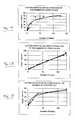
- FIGS. 1A-1Gare graphical representations comparing the speed of cutting silicon with a Q-switch Nd:YAG laser varies according to the atmosphere in which the cutting is accomplished.
- FIG. 3is a cross-sectional view of a portion of the apparatus of FIG. 2;
- FIG. 4is a cross-sectional view of the O-ring that forms part of the FIG. 2 apparatus;
- the laserWhen using a laser to cut silicon or any other material in air, the laser must be operated so as to provide a peak power density at the beam focus that is less than that which will cause the air to break down and form a plasma, which occurs at a power density of approximately 5 ⁇ 10 9 watts per square centimeter (W/cm 2 ).
- the formation of plasmaconsumes substantially all or most of the laser energy, thereby preventing laser cutting since little of the energy reaches the material to be cut. It has been determined from laser cutting in air that, in general, the HAZ becomes smaller for any given material at a peak power density just below that at which air breaks down into a plasma. Nevertheless, as noted above, the laser pulse energy must be maintained near the melting threshold to minimize the HAZ.
- FIGS. 1A-1Ggraphically show the results for material removal in a vacuum and all but two of the various gases listed above.
- FIGS. 1A-1Gpresent graphical data only for helium (He) and argon (AR).
- neon (Ne) and krypton (KR)were also tested and showed essentially identical behavior.
- nitrogenwas also tested to see if oxygen could be responsible for the poor cutting speed in an air ambient.
- Forming gaswas used to determine if hydrogen could accelerate the cutting speed, and the forming gas turned out to show essentially the same behavior as noble gases.
- Di-fluoromethanewas tested as an ambient to determine if free fluorine radicals produced by laser energy could accelerate the cutting process.
- Optical microscopy combined with cleaving and metallurgical cross-sectioningwas used to determine the shape of the laser cut, the presence of melt or slag and the presence of microcracks.
- the testsrevealed that cutting in a helium environment proceeded without microcracking to a depth of about 200 microns ( ⁇ m), with nearly vertical sidewalls except at the very beginning of the cutting action.
- the bottom of the cutis also “V” shaped and some buildup of slag and silicon is observed at the edges. It was observed also that with a cutting penetration deeper than about 200 microns, buildup of slag is observed at the walls of the kerf (i.e., the cut), thereby restricting beam access at the bottom of the cut and ultimately limiting the thickness which can be cut.
- EFG tubesmay measure six feet in length (or even longer) and, in the case of cylinders, more than three feet in diameter. It would normally be necessary to immerse the entire cylinder in a helium filled chamber with the laser beam entering through a window in the chamber. With such an arrangement the chamber would have to be filled with helium for every tube to be cut, unless a load lock including vacuum pumping of the lock is used. Because the expense and complexity of such apparatus is economically prohibitive for the cutting of wafers from an EFG tube for the production of solar cells, other apparatus has been conceived for practicing the invention.
- a second elastic and resilient tube 26made of plastic or rubber is embedded inside the O-ring.
- This plastic tube 26is connected to means (not shown) for (a) partially evacuating it so as to cause the inner circumference of the seal to expand, or (b) pressurizing it with air to cause the inner circumference of the O-ring to shrink.
- vacuumis applied to tube 26 so as to cause the O-ring to contract in cross-section while expanding its major diameter at its inner circumference.
- FIG. 5shows a modification of the foregoing apparatus.
- the helium, or other noble gas or forming gasis injected by tube 18 into the collar via an opening 30 in its top side directly above window 28 , and two vertical wipers 32 made of soft foam rubber similar to that of the seal 22 are located inside the collar on both sides of the beam impact area, preferably immediately adjacent to the opposite side edges of the window as shown in FIG. 5 .
- the wipers 32serve to prevent helium from filling the entire annulus of the collar, thus reducing the quantity of helium required to flood the space in front of the portion of the silicon tube being cut by the laser beam.
- the wipersmay be provided with embedded porous plastic tubes (not shown) like tube 24 that are connected to a water supply (not shown) via a suitable control valve (not shown) and serve to feed water to the wipers to keep them wet, thereby establishing a meniscus between the wipers and the silicon tube that acts to prevent escape of helium past the wipers.
- the cylindrical lensis rotated 90 degrees to its second position, in which position it focuses the laser beam so that its elongate beam spot is oriented with its long dimension extending horizontally, i.e., at a right angle to the axis of silicon cylinder 10 .
- This horizontally-oriented laser beam spotis caused to traverse cylinder 10 horizontally between the vertical cuts so as to separate wafers from the cylinder.
- Thiscan be achieved by rotating the silicon cylinder.
- itcan be achieved by pivoting mirror 40 on a pivot axis that extends parallel to the silicon cylinder. Regardless of how the horizontal cuts are made, only one line of horizontal cuts is required to produce wafers, since the bottom edges of the wafers are portions of the bottom edge of the silicon cylinder.
- FIG. 6schematically illustrates a gas assist nozzle 50 .
- the nozzlehas a central or axial bore 52 in which is mounted a focusing lens 54 .
- Bore 52is open at one end 56 for admittance of a laser beam from a laser (not shown) and has a reduced diameter discharge opening or orifice 58 through which the laser beam passes out of the nozzle.
- the lens 54serves to focus the laser beam so that its focal plane is at the adjacent surface of the material to be cut which will be located close to the discharge orifice 58 .
- One or more side ports 60are provided in the nozzle for injection of assist gas from a gas supply 21 .
- the assist gasis a noble gas or forming gas as described above.
- the Q-switched Nd:YAG laserhas been described in the foregoing specification as operating at a pulse repetition rate of 50 Hz and a 10 ns duration, with an average power output of 65 watts, it is to be appreciated that the laser may be operated with different pulse repetition rates, pulse durations and average power output, according to the material being cut and the results intended to be achieved. Also, the spot size and shape of the laser beam focused on the material to be cut may be altered according to the type of laser used, the desired cutting speed, the pulse width, repetition rate, and energy density, and the composition and thickness of the material being cut. While a circular beam spot pattern may be used advantageously with other lasers and the present invention, an elongated narrow spot pattern is preferred for the purpose of maximizing cutting speed.
- the beam spot patternis shaped so that the width of the cut made in the material being cut is in the order of microns.
- the width of the cut made in the material being cutis in the order of microns.
- a further possible modificationis to form the collar 16 so that its bottom side is closed off, i.e., so that in cross-section it consists of a top wall and a bottom wall connected by a side wall in the form of a “U” that is turned 90° on its side. It should be noted also that laser nozzles of different constructions may be used in practicing the invention.
- FIG. 2illustrates the invention as being applied to a cylinder rather than to a tube with a polygonal cross-section, e.g., an octagon
- the inventionmay be used to cut tubes of various cross-sectional configurations, e.g., eight-sided EFG-grown silicon tubes commonly identified simply as “octagons”, particularly if an assist gas nozzle as shown in FIG. 6 is used rather than a collar as illustrated in FIGS. 2 and 3.
- a collarmay still be used to provide a suitable noble gas or forming gas environment in the cutting zone, but in that case the collar will be constructed modified so that at its inner edge will have a mating polygonal configuration to provide a close fit with the tubes to be cut. It is to be noted that use of a collar is preferred over a gas assist nozzle since the latter would consume more of the forming gas or noble gas due to loss of gas to the outside atmosphere.
- the gaseous environment provided by the present inventionmay consist or a mixture of noble gases or a mixture of forming gas and one or more noble gases. Also although xenon was not tested, it is believed that its use would provide the same improvement in results that are obtained with helium, neon, argon and krypton.
- the inventionhas been described in connection with cutting silicon, it is believed that the concept of cutting a fragile crystalline material with a laser using a selected non-air ambient or environment may be used to cut other materials. Also the invention is not limited to cutting hollow tubes but may be used to cut silicon or other crystalline materials in sheet or other form, particularly materials having a relatively small thickness, e.g., a thickness in the range of 100 to 700 ⁇ m. Similarly, the apparatus used to support the silicon tubes and the construction of the laser system may be modified to use means well known or obvious to persons skilled in the art. Still other modifications will be obvious to persons skilled in the art from the foregoing description.
- laser beamand “laser energy beam” is to be construed as including a stream of pulses of laser energy.
Landscapes
- Engineering & Computer Science (AREA)
- Physics & Mathematics (AREA)
- Plasma & Fusion (AREA)
- Optics & Photonics (AREA)
- Mechanical Engineering (AREA)
- Condensed Matter Physics & Semiconductors (AREA)
- General Physics & Mathematics (AREA)
- Manufacturing & Machinery (AREA)
- Computer Hardware Design (AREA)
- Microelectronics & Electronic Packaging (AREA)
- Power Engineering (AREA)
- Laser Beam Processing (AREA)
Abstract
Description
Claims (26)
Priority Applications (6)
| Application Number | Priority Date | Filing Date | Title |
|---|---|---|---|
| US09/626,708US6376797B1 (en) | 2000-07-26 | 2000-07-26 | Laser cutting of semiconductor materials |
| CNB018021859ACN1185076C (en) | 2000-07-26 | 2001-05-14 | Laser cutting of semiconductor materials |
| AU61583/01AAU764787B2 (en) | 2000-07-26 | 2001-05-14 | Laser cutting of semiconductor materials |
| EP01935492AEP1303377A4 (en) | 2000-07-26 | 2001-05-14 | LASER CUTTING OF SEMICONDUCTOR MATERIALS |
| JP2002513648AJP4242642B2 (en) | 2000-07-26 | 2001-05-14 | Laser cutting of semiconductor materials |
| PCT/US2001/015566WO2002007927A1 (en) | 2000-07-26 | 2001-05-14 | Laser cutting of semiconductor materials |
Applications Claiming Priority (1)
| Application Number | Priority Date | Filing Date | Title |
|---|---|---|---|
| US09/626,708US6376797B1 (en) | 2000-07-26 | 2000-07-26 | Laser cutting of semiconductor materials |
Publications (1)
| Publication Number | Publication Date |
|---|---|
| US6376797B1true US6376797B1 (en) | 2002-04-23 |
Family
ID=24511494
Family Applications (1)
| Application Number | Title | Priority Date | Filing Date |
|---|---|---|---|
| US09/626,708Expired - LifetimeUS6376797B1 (en) | 2000-07-26 | 2000-07-26 | Laser cutting of semiconductor materials |
Country Status (6)
| Country | Link |
|---|---|
| US (1) | US6376797B1 (en) |
| EP (1) | EP1303377A4 (en) |
| JP (1) | JP4242642B2 (en) |
| CN (1) | CN1185076C (en) |
| AU (1) | AU764787B2 (en) |
| WO (1) | WO2002007927A1 (en) |
Cited By (61)
| Publication number | Priority date | Publication date | Assignee | Title |
|---|---|---|---|---|
| US20030155328A1 (en)* | 2002-02-15 | 2003-08-21 | Huth Mark C. | Laser micromachining and methods and systems of same |
| US6770544B2 (en)* | 2001-02-21 | 2004-08-03 | Nec Machinery Corporation | Substrate cutting method |
| US20040154638A1 (en)* | 2003-02-07 | 2004-08-12 | Steven Reder | Method to use a laser to perform the edge clean operation on a semiconductor wafer |
| US20040164061A1 (en)* | 2002-05-07 | 2004-08-26 | Masaya Takeuchi | Finishing machine using laser beam |
| US20040227794A1 (en)* | 2003-05-13 | 2004-11-18 | Pollard Jeffrey R | Laser micromachining and methods of same |
| US20050067393A1 (en)* | 2001-08-22 | 2005-03-31 | Matile Olivier | Method and installation for laser beam cutting using a multiple-focus objective and a convergent/divergent nozzle |
| WO2005053895A1 (en) | 2003-12-05 | 2005-06-16 | Spi Lasers Uk Limited | Apparatus for the industrial processing of a material by optical radiation |
| US20050173387A1 (en)* | 2000-09-13 | 2005-08-11 | Hamamatsu Photonics K.K. | Laser processing method and laser processing apparatus |
| WO2005036601A3 (en)* | 2003-10-07 | 2005-08-18 | Midwest Research Inst | Wafer characteristics via reflectomeytry and wafer processing apparatus and method |
| US20050202596A1 (en)* | 2002-03-12 | 2005-09-15 | Fumitsugu Fukuyo | Laser processing method |
| NL1025786C2 (en)* | 2004-03-22 | 2005-09-26 | Fico Bv | Laser cutting method for removing electronic components from lead board, uses inert gas atmosphere containing laser activated reagent |
| US6969822B2 (en) | 2003-05-13 | 2005-11-29 | Hewlett-Packard Development Company, L.P. | Laser micromachining systems |
| US20050272223A1 (en)* | 2002-03-12 | 2005-12-08 | Yoshimaro Fujii | Method for dicing substrate |
| US20060091126A1 (en)* | 2001-01-31 | 2006-05-04 | Baird Brian W | Ultraviolet laser ablative patterning of microstructures in semiconductors |
| US20060148212A1 (en)* | 2002-12-03 | 2006-07-06 | Fumitsugu Fukuyo | Method for cutting semiconductor substrate |
| US7157038B2 (en)* | 2000-09-20 | 2007-01-02 | Electro Scientific Industries, Inc. | Ultraviolet laser ablative patterning of microstructures in semiconductors |
| US20070125757A1 (en)* | 2003-03-12 | 2007-06-07 | Fumitsugu Fukuyo | Laser beam machining method |
| US20070158314A1 (en)* | 2003-03-12 | 2007-07-12 | Kenshi Fukumitsu | Laser processing method |
| US20070289381A1 (en)* | 2004-04-16 | 2007-12-20 | Oliver Bolzmann | Method for Operating a Sensor |
| US20080014661A1 (en)* | 2006-07-11 | 2008-01-17 | Michael Haag | Method for the manufacture of solar panels and special transport carrier |
| US20080096367A1 (en)* | 2004-10-05 | 2008-04-24 | Koninklijke Philips Electronics, N.V. | Method for Laser Dicing of a Substrate |
| US20080102605A1 (en)* | 2006-10-27 | 2008-05-01 | Evergreen Solar, Inc. | Method and Apparatus for Forming a Silicon Wafer |
| US20080264912A1 (en)* | 2004-05-27 | 2008-10-30 | Linde Aktiengesellschaft | Gas Mixture For Laser Beam Fusion Cutting |
| US20090025787A1 (en)* | 2007-07-27 | 2009-01-29 | Evergreen Solar, Inc. | Wafer/Ribbon Crystal Method and Apparatus |
| US20100059693A1 (en)* | 2008-09-09 | 2010-03-11 | Applied Materials, Inc. | Scribe process monitoring methodology |
| US20100102044A1 (en)* | 2006-09-27 | 2010-04-29 | Yoji Takizawa | Film cutting apparatus and film cutting method |
| US20100135341A1 (en)* | 2007-05-04 | 2010-06-03 | Ekspla Ltd. | Multiple Output Repetitively Pulsed Laser |
| CN1610068B (en)* | 2003-05-26 | 2011-08-03 | 株式会社迪斯科 | Method for Separating Non-Metallic Substrates |
| CN102310285A (en)* | 2011-07-27 | 2012-01-11 | 苏州德龙激光有限公司 | Laser processing device of silicon glass bonding slice and method thereof |
| USRE43400E1 (en) | 2000-09-20 | 2012-05-22 | Electro Scientific Industries, Inc. | Laser segmented cutting, multi-step cutting, or both |
| US20120145686A1 (en)* | 2008-03-31 | 2012-06-14 | Electro Scientific Industries, Inc. | On-The-Fly Manipulation Of Spot Size And Cutting Speed For Real-Time Control Of Trench Depth And Width In Laser Operations |
| US8247734B2 (en) | 2003-03-11 | 2012-08-21 | Hamamatsu Photonics K.K. | Laser beam machining method |
| US8278189B2 (en) | 2010-09-02 | 2012-10-02 | United Microelectronics Corp. | Method for thinning wafer |
| US8318579B1 (en) | 2011-12-01 | 2012-11-27 | United Microelectronics Corp. | Method for fabricating semiconductor device |
| US8466000B2 (en) | 2011-04-14 | 2013-06-18 | United Microelectronics Corp. | Backside-illuminated image sensor and fabricating method thereof |
| US20140076299A1 (en)* | 2012-09-20 | 2014-03-20 | Apple Inc. | Multi-step cutting process |
| US8779344B2 (en) | 2012-07-11 | 2014-07-15 | United Microelectronics Corp. | Image sensor including a deep trench isolation (DTI)that does not contact a connecting element physically |
| US8779484B2 (en) | 2012-11-29 | 2014-07-15 | United Microelectronics Corp. | Image sensor and process thereof |
| US8815102B2 (en) | 2012-03-23 | 2014-08-26 | United Microelectronics Corporation | Method for fabricating patterned dichroic film |
| US8828779B2 (en) | 2012-11-01 | 2014-09-09 | United Microelectronics Corp. | Backside illumination (BSI) CMOS image sensor process |
| US9054106B2 (en) | 2013-11-13 | 2015-06-09 | United Microelectronics Corp. | Semiconductor structure and method for manufacturing the same |
| US9070612B2 (en) | 2011-07-05 | 2015-06-30 | United Microelectronics Corporation | Method for fabricating optical micro structure and applications thereof |
| US9129876B2 (en) | 2013-05-28 | 2015-09-08 | United Microelectronics Corp. | Image sensor and process thereof |
| WO2016033494A1 (en)* | 2014-08-28 | 2016-03-03 | Ipg Photonics Corporation | System and method for laser beveling and/or polishing |
| US9279923B2 (en) | 2013-03-26 | 2016-03-08 | United Microelectronics Corporation | Color filter layer and method of fabricating the same |
| US9312292B2 (en) | 2011-10-26 | 2016-04-12 | United Microelectronics Corp. | Back side illumination image sensor and manufacturing method thereof |
| US9401441B2 (en) | 2012-06-14 | 2016-07-26 | United Microelectronics Corporation | Back-illuminated image sensor with dishing depression surface |
| US9537040B2 (en) | 2013-05-09 | 2017-01-03 | United Microelectronics Corp. | Complementary metal-oxide-semiconductor image sensor and manufacturing method thereof |
| CN106312321A (en)* | 2016-11-16 | 2017-01-11 | 哈尔滨工业大学 | A local vacuum laser welding device for pipeline circular seams and a welding method based on the welding device |
| US9764427B2 (en) | 2014-02-28 | 2017-09-19 | Ipg Photonics Corporation | Multi-laser system and method for cutting and post-cut processing hard dielectric materials |
| US9841319B2 (en) | 2013-11-19 | 2017-12-12 | United Microelectronics Corp. | Light detecting device |
| US9844833B2 (en) | 2014-01-30 | 2017-12-19 | Apple Inc. | System and method for laser cutting sapphire using multiple gas media |
| US9956646B2 (en) | 2014-02-28 | 2018-05-01 | Ipg Photonics Corporation | Multiple-beam laser processing using multiple laser beams with distinct wavelengths and/or pulse durations |
| US10144107B2 (en) | 2015-09-30 | 2018-12-04 | Apple Inc. | Ultrasonic polishing systems and methods of polishing brittle components for electronic devices |
| US10286487B2 (en) | 2013-02-28 | 2019-05-14 | Ipg Photonics Corporation | Laser system and method for processing sapphire |
| US10343237B2 (en) | 2014-02-28 | 2019-07-09 | Ipg Photonics Corporation | System and method for laser beveling and/or polishing |
| US10639746B1 (en) | 2014-06-20 | 2020-05-05 | Apple Inc. | Ceramic-based components having laser-etched markings |
| US10807199B2 (en) | 2014-08-28 | 2020-10-20 | Ipg Photonics Corporation | Multi-laser system and method for cutting and post-cut processing hard dielectric materials |
| US11113494B2 (en) | 2019-11-11 | 2021-09-07 | Apple Inc. | Biometric key including a textured ceramic cover |
| US11498156B2 (en)* | 2014-07-03 | 2022-11-15 | Nippon Steel Corporation | Laser processing apparatus |
| US11734942B2 (en) | 2019-11-11 | 2023-08-22 | Apple Inc. | Biometric key including a textured ceramic cover |
Families Citing this family (10)
| Publication number | Priority date | Publication date | Assignee | Title |
|---|---|---|---|---|
| GB2404280B (en)* | 2003-07-03 | 2006-09-27 | Xsil Technology Ltd | Die bonding |
| JP4563097B2 (en) | 2003-09-10 | 2010-10-13 | 浜松ホトニクス株式会社 | Semiconductor substrate cutting method |
| JP4890746B2 (en)* | 2004-06-14 | 2012-03-07 | 株式会社ディスコ | Wafer processing method |
| JP2006108459A (en)* | 2004-10-07 | 2006-04-20 | Disco Abrasive Syst Ltd | Laser processing method and laser processing apparatus for silicon wafer |
| CN102284792B (en)* | 2011-07-26 | 2013-11-13 | 江苏捷捷微电子股份有限公司 | Device for scraping and cutting on semiconductor device chip glass passive film and using method thereof |
| JP6000700B2 (en)* | 2012-07-10 | 2016-10-05 | 株式会社ディスコ | Laser processing method |
| DE102015118042A1 (en) | 2015-10-22 | 2017-04-27 | Nexwafe Gmbh | Method and device for producing a semiconductor layer |
| EP3507057A1 (en)* | 2016-08-30 | 2019-07-10 | Corning Incorporated | Laser processing of transparent materials |
| CN109216508A (en)* | 2018-11-16 | 2019-01-15 | 常州大学 | A method of inhibit crystal silicon solar batteries laser to cut the reduction of half behind efficiency |
| CN115346864A (en)* | 2022-07-15 | 2022-11-15 | 惠州佰维存储科技有限公司 | Method for grinding wafer |
Citations (11)
| Publication number | Priority date | Publication date | Assignee | Title |
|---|---|---|---|---|
| US4532401A (en)* | 1982-03-31 | 1985-07-30 | Tokyo Shibaura Denki Kabushiki Kaisha | Apparatus and method for cutting a wiring pattern |
| US4728771A (en) | 1978-01-03 | 1988-03-01 | Prima Industrie S.P.A. | Automatic cutting machine using laser ray |
| US4871897A (en) | 1986-09-01 | 1989-10-03 | Instituttet For Produktudvikling | Nozzle for laser processing |
| US5083066A (en) | 1988-08-02 | 1992-01-21 | Fanuc Ltd. | Method of controlling synchronous operation of machine tool |
| US5168143A (en)* | 1990-01-29 | 1992-12-01 | E. I. Du Pont De Nemours And Company | Method for laser cutting metal plates |
| US5220149A (en) | 1990-10-06 | 1993-06-15 | Trumpf Gmbh & Co. | Laser nozzle |
| US5227604A (en)* | 1991-06-28 | 1993-07-13 | Digital Equipment Corporation | Atmospheric pressure gaseous-flux-assisted laser reflow soldering |
| US5374803A (en) | 1989-10-12 | 1994-12-20 | Kabushiki Kaisha Komatsu Seisakusho | Laser cutting process |
| US5869803A (en)* | 1993-11-02 | 1999-02-09 | Sony Corporation | Method of forming polycrystalline silicon layer on substrate and surface treatment apparatus thereof |
| US6163010A (en)* | 1996-10-25 | 2000-12-19 | E. I. Du Pont De Nemours And Company | Method and apparatus for laser cutting materials |
| US6252197B1 (en)* | 1998-12-01 | 2001-06-26 | Accudyne Display And Semiconductor Systems, Inc. | Method and apparatus for separating non-metallic substrates utilizing a supplemental mechanical force applicator |
Family Cites Families (2)
| Publication number | Priority date | Publication date | Assignee | Title |
|---|---|---|---|---|
| EP0857098A1 (en)* | 1995-10-27 | 1998-08-12 | E.I. Du Pont De Nemours And Company | Method and apparatus for laser cutting materials |
| DE19730028C2 (en)* | 1997-07-14 | 2002-12-12 | Deutsche Telekom Ag | Method for separating and processing semiconductor chips made of A III-B V compound semiconductors produced on a semiconductor substrate in the assembly using an excimer laser |
- 2000
- 2000-07-26USUS09/626,708patent/US6376797B1/ennot_activeExpired - Lifetime
- 2001
- 2001-05-14WOPCT/US2001/015566patent/WO2002007927A1/enactiveIP Right Grant
- 2001-05-14JPJP2002513648Apatent/JP4242642B2/ennot_activeExpired - Fee Related
- 2001-05-14EPEP01935492Apatent/EP1303377A4/ennot_activeWithdrawn
- 2001-05-14CNCNB018021859Apatent/CN1185076C/ennot_activeExpired - Fee Related
- 2001-05-14AUAU61583/01Apatent/AU764787B2/ennot_activeCeased
Patent Citations (11)
| Publication number | Priority date | Publication date | Assignee | Title |
|---|---|---|---|---|
| US4728771A (en) | 1978-01-03 | 1988-03-01 | Prima Industrie S.P.A. | Automatic cutting machine using laser ray |
| US4532401A (en)* | 1982-03-31 | 1985-07-30 | Tokyo Shibaura Denki Kabushiki Kaisha | Apparatus and method for cutting a wiring pattern |
| US4871897A (en) | 1986-09-01 | 1989-10-03 | Instituttet For Produktudvikling | Nozzle for laser processing |
| US5083066A (en) | 1988-08-02 | 1992-01-21 | Fanuc Ltd. | Method of controlling synchronous operation of machine tool |
| US5374803A (en) | 1989-10-12 | 1994-12-20 | Kabushiki Kaisha Komatsu Seisakusho | Laser cutting process |
| US5168143A (en)* | 1990-01-29 | 1992-12-01 | E. I. Du Pont De Nemours And Company | Method for laser cutting metal plates |
| US5220149A (en) | 1990-10-06 | 1993-06-15 | Trumpf Gmbh & Co. | Laser nozzle |
| US5227604A (en)* | 1991-06-28 | 1993-07-13 | Digital Equipment Corporation | Atmospheric pressure gaseous-flux-assisted laser reflow soldering |
| US5869803A (en)* | 1993-11-02 | 1999-02-09 | Sony Corporation | Method of forming polycrystalline silicon layer on substrate and surface treatment apparatus thereof |
| US6163010A (en)* | 1996-10-25 | 2000-12-19 | E. I. Du Pont De Nemours And Company | Method and apparatus for laser cutting materials |
| US6252197B1 (en)* | 1998-12-01 | 2001-06-26 | Accudyne Display And Semiconductor Systems, Inc. | Method and apparatus for separating non-metallic substrates utilizing a supplemental mechanical force applicator |
Cited By (146)
| Publication number | Priority date | Publication date | Assignee | Title |
|---|---|---|---|---|
| US20110027972A1 (en)* | 2000-09-13 | 2011-02-03 | Hamamatsu Photonics K.K. | Method of cutting a substrate and method of manufacturing a semiconductor device |
| US20110021004A1 (en)* | 2000-09-13 | 2011-01-27 | Hamamatsu Photonics K.K. | Method of cutting a substrate, method of cutting a wafer-like object, and method of manufacturing a semiconductor device |
| US8933369B2 (en) | 2000-09-13 | 2015-01-13 | Hamamatsu Photonics K.K. | Method of cutting a substrate and method of manufacturing a semiconductor device |
| US8927900B2 (en) | 2000-09-13 | 2015-01-06 | Hamamatsu Photonics K.K. | Method of cutting a substrate, method of processing a wafer-like object, and method of manufacturing a semiconductor device |
| US8946591B2 (en) | 2000-09-13 | 2015-02-03 | Hamamatsu Photonics K.K. | Method of manufacturing a semiconductor device formed using a substrate cutting method |
| US7592238B2 (en) | 2000-09-13 | 2009-09-22 | Hamamatsu Photonics K.K. | Laser processing method and laser processing apparatus |
| US8946589B2 (en) | 2000-09-13 | 2015-02-03 | Hamamatsu Photonics K.K. | Method of cutting a substrate, method of cutting a wafer-like object, and method of manufacturing a semiconductor device |
| US8946592B2 (en) | 2000-09-13 | 2015-02-03 | Hamamatsu Photonics K.K. | Laser processing method and laser processing apparatus |
| US20050173387A1 (en)* | 2000-09-13 | 2005-08-11 | Hamamatsu Photonics K.K. | Laser processing method and laser processing apparatus |
| US8969761B2 (en) | 2000-09-13 | 2015-03-03 | Hamamatsu Photonics K.K. | Method of cutting a wafer-like object and semiconductor chip |
| US20050181581A1 (en)* | 2000-09-13 | 2005-08-18 | Hamamatsu Photonics K.K. | Laser processing method and laser processing apparatus |
| US20050184037A1 (en)* | 2000-09-13 | 2005-08-25 | Hamamatsu Photonics K.K. | Laser processing method and laser processing apparatus |
| US20050189330A1 (en)* | 2000-09-13 | 2005-09-01 | Hamamatsu Photonics K.K. | Laser processing method and laser processing apparatus |
| US20050194364A1 (en)* | 2000-09-13 | 2005-09-08 | Hamamatsu Photonics K.K. | Laser processing method and laser processing apparatus |
| US8716110B2 (en) | 2000-09-13 | 2014-05-06 | Hamamatsu Photonics K.K. | Laser processing method and laser processing apparatus |
| US7626137B2 (en) | 2000-09-13 | 2009-12-01 | Hamamatsu Photonics K.K. | Laser cutting by forming a modified region within an object and generating fractures |
| US8937264B2 (en) | 2000-09-13 | 2015-01-20 | Hamamatsu Photonics K.K. | Laser processing method and laser processing apparatus |
| US8283595B2 (en) | 2000-09-13 | 2012-10-09 | Hamamatsu Photonics K.K. | Laser processing method and laser processing apparatus |
| US7547613B2 (en) | 2000-09-13 | 2009-06-16 | Hamamatsu Photonics K.K. | Laser processing method and laser processing apparatus |
| US20060040473A1 (en)* | 2000-09-13 | 2006-02-23 | Hamamatsu Photonics K.K. | Laser processing method and laser processing apparatus |
| US20100055876A1 (en)* | 2000-09-13 | 2010-03-04 | Hamamatsu Photonics K.K. | Laser processing method and laser processing apparatus |
| US10796959B2 (en) | 2000-09-13 | 2020-10-06 | Hamamatsu Photonics K.K. | Laser processing method and laser processing apparatus |
| US7732730B2 (en) | 2000-09-13 | 2010-06-08 | Hamamatsu Photonics K.K. | Laser processing method and laser processing apparatus |
| US20100176100A1 (en)* | 2000-09-13 | 2010-07-15 | Hamamatsu Photonics K.K. | Laser processing method and laser processing apparatus |
| US20060160331A1 (en)* | 2000-09-13 | 2006-07-20 | Hamamatsu Photonics K.K. | Laser processing method and laser processing apparatus |
| US7825350B2 (en) | 2000-09-13 | 2010-11-02 | Hamamatsu Photonics K.K. | Laser processing method and laser processing apparatus |
| US9837315B2 (en) | 2000-09-13 | 2017-12-05 | Hamamatsu Photonics K.K. | Laser processing method and laser processing apparatus |
| US8227724B2 (en) | 2000-09-13 | 2012-07-24 | Hamamatsu Photonics K.K. | Laser processing method and laser processing apparatus |
| US20110037149A1 (en)* | 2000-09-13 | 2011-02-17 | Hamamatsu Photonics K.K. | Method of cutting a wafer-like object and semiconductor chip |
| US20110027971A1 (en)* | 2000-09-13 | 2011-02-03 | Hamamatsu Photonics K.K. | Method of cutting a substrate, method of processing a wafer-like object, and method of manufacturing a semiconductor device |
| US7615721B2 (en) | 2000-09-13 | 2009-11-10 | Hamamatsu Photonics K.K. | Laser processing method and laser processing apparatus |
| US7157038B2 (en)* | 2000-09-20 | 2007-01-02 | Electro Scientific Industries, Inc. | Ultraviolet laser ablative patterning of microstructures in semiconductors |
| USRE43400E1 (en) | 2000-09-20 | 2012-05-22 | Electro Scientific Industries, Inc. | Laser segmented cutting, multi-step cutting, or both |
| USRE43487E1 (en) | 2000-09-20 | 2012-06-26 | Electro Scientific Industries, Inc. | Laser segmented cutting |
| USRE43605E1 (en) | 2000-09-20 | 2012-08-28 | Electro Scientific Industries, Inc. | Laser segmented cutting, multi-step cutting, or both |
| US20060091126A1 (en)* | 2001-01-31 | 2006-05-04 | Baird Brian W | Ultraviolet laser ablative patterning of microstructures in semiconductors |
| US6770544B2 (en)* | 2001-02-21 | 2004-08-03 | Nec Machinery Corporation | Substrate cutting method |
| US20050067393A1 (en)* | 2001-08-22 | 2005-03-31 | Matile Olivier | Method and installation for laser beam cutting using a multiple-focus objective and a convergent/divergent nozzle |
| US20060049156A1 (en)* | 2002-02-15 | 2006-03-09 | Michael Mulloy | Method of forming substrate for fluid ejection device |
| US20030155328A1 (en)* | 2002-02-15 | 2003-08-21 | Huth Mark C. | Laser micromachining and methods and systems of same |
| US8653410B2 (en) | 2002-02-15 | 2014-02-18 | Hewlett-Packard Development Company, L.P. | Method of forming substrate for fluid ejection device |
| US9543256B2 (en) | 2002-03-12 | 2017-01-10 | Hamamatsu Photonics K.K. | Substrate dividing method |
| US8598015B2 (en) | 2002-03-12 | 2013-12-03 | Hamamatsu Photonics K.K. | Laser processing method |
| US7566635B2 (en) | 2002-03-12 | 2009-07-28 | Hamamatsu Photonics K.K. | Substrate dividing method |
| US11424162B2 (en) | 2002-03-12 | 2022-08-23 | Hamamatsu Photonics K.K. | Substrate dividing method |
| US8889525B2 (en) | 2002-03-12 | 2014-11-18 | Hamamatsu Photonics K.K. | Substrate dividing method |
| US8802543B2 (en) | 2002-03-12 | 2014-08-12 | Hamamatsu Photonics K.K. | Laser processing method |
| US10622255B2 (en) | 2002-03-12 | 2020-04-14 | Hamamatsu Photonics K.K. | Substrate dividing method |
| US9142458B2 (en) | 2002-03-12 | 2015-09-22 | Hamamatsu Photonics K.K. | Substrate dividing method |
| US7749867B2 (en) | 2002-03-12 | 2010-07-06 | Hamamatsu Photonics K.K. | Method of cutting processed object |
| US20050202596A1 (en)* | 2002-03-12 | 2005-09-15 | Fumitsugu Fukuyo | Laser processing method |
| US20080090382A1 (en)* | 2002-03-12 | 2008-04-17 | Hamamatsu Photonics K.K. | Substrate dividing method |
| US20100203707A1 (en)* | 2002-03-12 | 2010-08-12 | Hamamatsu Photonics K.K. | Substrate dividing method |
| US9287177B2 (en) | 2002-03-12 | 2016-03-15 | Hamamatsu Photonics K.K. | Substrate dividing method |
| US8673745B2 (en) | 2002-03-12 | 2014-03-18 | Hamamatsu Photonics K.K. | Method of cutting object to be processed |
| US8551865B2 (en) | 2002-03-12 | 2013-10-08 | Hamamatsu Photonics K.K. | Method of cutting an object to be processed |
| US8518801B2 (en) | 2002-03-12 | 2013-08-27 | Hamamatsu Photonics K.K. | Substrate dividing method |
| US8519511B2 (en) | 2002-03-12 | 2013-08-27 | Hamamatsu Photonics K.K. | Substrate dividing method |
| US10068801B2 (en) | 2002-03-12 | 2018-09-04 | Hamamatsu Photonics K.K. | Substrate dividing method |
| US8518800B2 (en) | 2002-03-12 | 2013-08-27 | Hamamatsu Photonics K.K. | Substrate dividing method |
| US9543207B2 (en) | 2002-03-12 | 2017-01-10 | Hamamatsu Photonics K.K. | Substrate dividing method |
| US9711405B2 (en) | 2002-03-12 | 2017-07-18 | Hamamatsu Photonics K.K. | Substrate dividing method |
| US8361883B2 (en)* | 2002-03-12 | 2013-01-29 | Hamamatsu Photonics K.K. | Laser processing method |
| US8183131B2 (en) | 2002-03-12 | 2012-05-22 | Hamamatsu Photonics K. K. | Method of cutting an object to be processed |
| US9553023B2 (en) | 2002-03-12 | 2017-01-24 | Hamamatsu Photonics K.K. | Substrate dividing method |
| US8314013B2 (en) | 2002-03-12 | 2012-11-20 | Hamamatsu Photonics K.K. | Semiconductor chip manufacturing method |
| US20060121697A1 (en)* | 2002-03-12 | 2006-06-08 | Hamamatsu Photonics K.K. | Substrate dividing method |
| US8304325B2 (en)* | 2002-03-12 | 2012-11-06 | Hamamatsu-Photonics K.K. | Substrate dividing method |
| US20060011593A1 (en)* | 2002-03-12 | 2006-01-19 | Fumitsugu Fukuyo | Method of cutting processed object |
| US20050272223A1 (en)* | 2002-03-12 | 2005-12-08 | Yoshimaro Fujii | Method for dicing substrate |
| US8268704B2 (en)* | 2002-03-12 | 2012-09-18 | Hamamatsu Photonics K.K. | Method for dicing substrate |
| US9548246B2 (en) | 2002-03-12 | 2017-01-17 | Hamamatsu Photonics K.K. | Substrate dividing method |
| US20040164061A1 (en)* | 2002-05-07 | 2004-08-26 | Masaya Takeuchi | Finishing machine using laser beam |
| US8450187B2 (en) | 2002-12-03 | 2013-05-28 | Hamamatsu Photonics K.K. | Method of cutting semiconductor substrate |
| US8263479B2 (en)* | 2002-12-03 | 2012-09-11 | Hamamatsu Photonics K.K. | Method for cutting semiconductor substrate |
| US20060148212A1 (en)* | 2002-12-03 | 2006-07-06 | Fumitsugu Fukuyo | Method for cutting semiconductor substrate |
| US8865566B2 (en) | 2002-12-03 | 2014-10-21 | Hamamatsu Photonics K.K. | Method of cutting semiconductor substrate |
| US8409968B2 (en) | 2002-12-03 | 2013-04-02 | Hamamatsu Photonics K.K. | Method of cutting semiconductor substrate via modified region formation and subsequent sheet expansion |
| US6874510B2 (en)* | 2003-02-07 | 2005-04-05 | Lsi Logic Corporation | Method to use a laser to perform the edge clean operation on a semiconductor wafer |
| US20040154638A1 (en)* | 2003-02-07 | 2004-08-12 | Steven Reder | Method to use a laser to perform the edge clean operation on a semiconductor wafer |
| US8247734B2 (en) | 2003-03-11 | 2012-08-21 | Hamamatsu Photonics K.K. | Laser beam machining method |
| US8969752B2 (en) | 2003-03-12 | 2015-03-03 | Hamamatsu Photonics K.K. | Laser processing method |
| US20070125757A1 (en)* | 2003-03-12 | 2007-06-07 | Fumitsugu Fukuyo | Laser beam machining method |
| US8685838B2 (en)* | 2003-03-12 | 2014-04-01 | Hamamatsu Photonics K.K. | Laser beam machining method |
| US20070158314A1 (en)* | 2003-03-12 | 2007-07-12 | Kenshi Fukumitsu | Laser processing method |
| US6969822B2 (en) | 2003-05-13 | 2005-11-29 | Hewlett-Packard Development Company, L.P. | Laser micromachining systems |
| US20040227794A1 (en)* | 2003-05-13 | 2004-11-18 | Pollard Jeffrey R | Laser micromachining and methods of same |
| US7754999B2 (en)* | 2003-05-13 | 2010-07-13 | Hewlett-Packard Development Company, L.P. | Laser micromachining and methods of same |
| CN1610068B (en)* | 2003-05-26 | 2011-08-03 | 株式会社迪斯科 | Method for Separating Non-Metallic Substrates |
| US7238912B2 (en) | 2003-10-07 | 2007-07-03 | Midwest Research Institute | Wafer characteristics via reflectometry and wafer processing apparatus and method |
| US20060219678A1 (en)* | 2003-10-07 | 2006-10-05 | Sopori Bhushan L | Wafer characteristics via reflectometry and wafer processing apparatus and method |
| WO2005036601A3 (en)* | 2003-10-07 | 2005-08-18 | Midwest Research Inst | Wafer characteristics via reflectomeytry and wafer processing apparatus and method |
| WO2005053895A1 (en) | 2003-12-05 | 2005-06-16 | Spi Lasers Uk Limited | Apparatus for the industrial processing of a material by optical radiation |
| US7592568B2 (en) | 2003-12-05 | 2009-09-22 | Spi Lasers Uk Ltd. | Apparatus for the industrial processing of a material by optical radiation |
| US20060219673A1 (en)* | 2003-12-05 | 2006-10-05 | Spi Lasers Uk Ltd | Apparatus for the industrial processing of a material by optical radiation |
| NL1025786C2 (en)* | 2004-03-22 | 2005-09-26 | Fico Bv | Laser cutting method for removing electronic components from lead board, uses inert gas atmosphere containing laser activated reagent |
| US20070289381A1 (en)* | 2004-04-16 | 2007-12-20 | Oliver Bolzmann | Method for Operating a Sensor |
| US20080264912A1 (en)* | 2004-05-27 | 2008-10-30 | Linde Aktiengesellschaft | Gas Mixture For Laser Beam Fusion Cutting |
| US20080096367A1 (en)* | 2004-10-05 | 2008-04-24 | Koninklijke Philips Electronics, N.V. | Method for Laser Dicing of a Substrate |
| US20080014661A1 (en)* | 2006-07-11 | 2008-01-17 | Michael Haag | Method for the manufacture of solar panels and special transport carrier |
| US20100102044A1 (en)* | 2006-09-27 | 2010-04-29 | Yoji Takizawa | Film cutting apparatus and film cutting method |
| US20080102605A1 (en)* | 2006-10-27 | 2008-05-01 | Evergreen Solar, Inc. | Method and Apparatus for Forming a Silicon Wafer |
| US7970026B2 (en) | 2007-05-04 | 2011-06-28 | Ekspla Ltd. | Multiple output repetitively pulsed laser |
| US20100135341A1 (en)* | 2007-05-04 | 2010-06-03 | Ekspla Ltd. | Multiple Output Repetitively Pulsed Laser |
| US20090025787A1 (en)* | 2007-07-27 | 2009-01-29 | Evergreen Solar, Inc. | Wafer/Ribbon Crystal Method and Apparatus |
| US20120145686A1 (en)* | 2008-03-31 | 2012-06-14 | Electro Scientific Industries, Inc. | On-The-Fly Manipulation Of Spot Size And Cutting Speed For Real-Time Control Of Trench Depth And Width In Laser Operations |
| US8723076B2 (en)* | 2008-03-31 | 2014-05-13 | Electro Scientific Industries, Inc. | On-the-fly manipulation of spot size and cutting speed for real-time control of trench depth and width in laser operations |
| US20100059693A1 (en)* | 2008-09-09 | 2010-03-11 | Applied Materials, Inc. | Scribe process monitoring methodology |
| US7956337B2 (en)* | 2008-09-09 | 2011-06-07 | Applied Materials, Inc. | Scribe process monitoring methodology |
| US8278189B2 (en) | 2010-09-02 | 2012-10-02 | United Microelectronics Corp. | Method for thinning wafer |
| US8466000B2 (en) | 2011-04-14 | 2013-06-18 | United Microelectronics Corp. | Backside-illuminated image sensor and fabricating method thereof |
| US9070612B2 (en) | 2011-07-05 | 2015-06-30 | United Microelectronics Corporation | Method for fabricating optical micro structure and applications thereof |
| CN102310285B (en)* | 2011-07-27 | 2014-05-14 | 苏州德龙激光股份有限公司 | Laser processing device of silicon glass bonding slice and method thereof |
| CN102310285A (en)* | 2011-07-27 | 2012-01-11 | 苏州德龙激光有限公司 | Laser processing device of silicon glass bonding slice and method thereof |
| US9312292B2 (en) | 2011-10-26 | 2016-04-12 | United Microelectronics Corp. | Back side illumination image sensor and manufacturing method thereof |
| US8318579B1 (en) | 2011-12-01 | 2012-11-27 | United Microelectronics Corp. | Method for fabricating semiconductor device |
| US8815102B2 (en) | 2012-03-23 | 2014-08-26 | United Microelectronics Corporation | Method for fabricating patterned dichroic film |
| US9401441B2 (en) | 2012-06-14 | 2016-07-26 | United Microelectronics Corporation | Back-illuminated image sensor with dishing depression surface |
| US9443902B1 (en) | 2012-06-14 | 2016-09-13 | United Microelectronics Corporation | Fabricating method of back-illuminated image sensor with dishing depression surface |
| US8779344B2 (en) | 2012-07-11 | 2014-07-15 | United Microelectronics Corp. | Image sensor including a deep trench isolation (DTI)that does not contact a connecting element physically |
| US20140076299A1 (en)* | 2012-09-20 | 2014-03-20 | Apple Inc. | Multi-step cutting process |
| US9120179B2 (en)* | 2012-09-20 | 2015-09-01 | Apple Inc. | Multi-step cutting process |
| US8828779B2 (en) | 2012-11-01 | 2014-09-09 | United Microelectronics Corp. | Backside illumination (BSI) CMOS image sensor process |
| US8779484B2 (en) | 2012-11-29 | 2014-07-15 | United Microelectronics Corp. | Image sensor and process thereof |
| US10286487B2 (en) | 2013-02-28 | 2019-05-14 | Ipg Photonics Corporation | Laser system and method for processing sapphire |
| US9279923B2 (en) | 2013-03-26 | 2016-03-08 | United Microelectronics Corporation | Color filter layer and method of fabricating the same |
| US9537040B2 (en) | 2013-05-09 | 2017-01-03 | United Microelectronics Corp. | Complementary metal-oxide-semiconductor image sensor and manufacturing method thereof |
| US9859328B2 (en) | 2013-05-09 | 2018-01-02 | United Microelectronics Corp. | Method of manufacturing a metal-oxide-semiconductor image sensor |
| US9129876B2 (en) | 2013-05-28 | 2015-09-08 | United Microelectronics Corp. | Image sensor and process thereof |
| US9054106B2 (en) | 2013-11-13 | 2015-06-09 | United Microelectronics Corp. | Semiconductor structure and method for manufacturing the same |
| US9841319B2 (en) | 2013-11-19 | 2017-12-12 | United Microelectronics Corp. | Light detecting device |
| US9844833B2 (en) | 2014-01-30 | 2017-12-19 | Apple Inc. | System and method for laser cutting sapphire using multiple gas media |
| US9956646B2 (en) | 2014-02-28 | 2018-05-01 | Ipg Photonics Corporation | Multiple-beam laser processing using multiple laser beams with distinct wavelengths and/or pulse durations |
| US10343237B2 (en) | 2014-02-28 | 2019-07-09 | Ipg Photonics Corporation | System and method for laser beveling and/or polishing |
| US9764427B2 (en) | 2014-02-28 | 2017-09-19 | Ipg Photonics Corporation | Multi-laser system and method for cutting and post-cut processing hard dielectric materials |
| US10639746B1 (en) | 2014-06-20 | 2020-05-05 | Apple Inc. | Ceramic-based components having laser-etched markings |
| US11498156B2 (en)* | 2014-07-03 | 2022-11-15 | Nippon Steel Corporation | Laser processing apparatus |
| WO2016033494A1 (en)* | 2014-08-28 | 2016-03-03 | Ipg Photonics Corporation | System and method for laser beveling and/or polishing |
| US10807199B2 (en) | 2014-08-28 | 2020-10-20 | Ipg Photonics Corporation | Multi-laser system and method for cutting and post-cut processing hard dielectric materials |
| US11565350B2 (en) | 2014-08-28 | 2023-01-31 | Ipg Photonics Corporation | System and method for laser beveling and/or polishing |
| US11819949B2 (en) | 2014-08-28 | 2023-11-21 | Ipg Photonics Corporation | Multi-laser system and method for cutting and post-cut processing hard dielectric materials |
| US10144107B2 (en) | 2015-09-30 | 2018-12-04 | Apple Inc. | Ultrasonic polishing systems and methods of polishing brittle components for electronic devices |
| CN106312321B (en)* | 2016-11-16 | 2017-11-17 | 哈尔滨工业大学 | Pipeline circumferential seam local vacuum laser welding device and welding method based on welding device |
| CN106312321A (en)* | 2016-11-16 | 2017-01-11 | 哈尔滨工业大学 | A local vacuum laser welding device for pipeline circular seams and a welding method based on the welding device |
| US11113494B2 (en) | 2019-11-11 | 2021-09-07 | Apple Inc. | Biometric key including a textured ceramic cover |
| US11734942B2 (en) | 2019-11-11 | 2023-08-22 | Apple Inc. | Biometric key including a textured ceramic cover |
Also Published As
| Publication number | Publication date |
|---|---|
| EP1303377A1 (en) | 2003-04-23 |
| WO2002007927A1 (en) | 2002-01-31 |
| AU764787B2 (en) | 2003-08-28 |
| CN1185076C (en) | 2005-01-19 |
| JP4242642B2 (en) | 2009-03-25 |
| EP1303377A4 (en) | 2009-08-05 |
| AU6158301A (en) | 2002-02-05 |
| JP2004504729A (en) | 2004-02-12 |
| CN1386081A (en) | 2002-12-18 |
Similar Documents
| Publication | Publication Date | Title |
|---|---|---|
| US6376797B1 (en) | Laser cutting of semiconductor materials | |
| US8198566B2 (en) | Laser processing of workpieces containing low-k dielectric material | |
| US6359254B1 (en) | Method for producing shaped hole in a structure | |
| Shirk et al. | A review of ultrashort pulsed laser ablation of materials | |
| US8143686B2 (en) | Laser-induced structuring of substrate surfaces | |
| US6229113B1 (en) | Method and apparatus for producing a laser drilled hole in a structure | |
| EP2576127B2 (en) | Process of engraving at least one groove for forming incipient fractures using a optical fibre laser device | |
| US20020190435A1 (en) | Laser segmented cutting | |
| US20120168412A1 (en) | Apparatus and method for forming an aperture in a substrate | |
| TW201729935A (en) | Method of laser machining a transparent material | |
| TWI548105B (en) | Method and apparatus for scribing a thin film layer of a cadmium telluride solar cell | |
| US6969822B2 (en) | Laser micromachining systems | |
| US8890025B2 (en) | Method and apparatus to scribe thin film layers of cadmium telluride solar cells | |
| Li et al. | Fibre laser microvia drilling and ablation of Si with tuneable pulse shapes | |
| Schoonderbeek et al. | Laser technology for cost reduction in silicon solar cell production | |
| US20020182877A1 (en) | Photo-processing of materials in the presence of reactive fluid | |
| Raciukaitis et al. | Micro-machining of silicon and glass with picosecond lasers | |
| Gobet et al. | Implementation of short-pulse lasers for wafer scribing and grooving applications | |
| Pauchard et al. | Advanced micromachining combining nanosecond lasers with water jet-guided laser technology | |
| Wang et al. | Ablation and cutting of silicon wafer and micro-mold fabrication using femtosecond laser pulses | |
| Temme et al. | Precision drilling of fused silica with 157-nm excimer laser radiation | |
| Huang et al. | Ytterbium-pulsed fiber laser percussion drilling silicon for emitter wrap through solar cells | |
| Saetang et al. | Laser micromachining of silicon substrates | |
| Kerrien et al. | MEMS applications of laser-induced ultra-shallow and ultraheavy boron-doping of silicon above the solid-solubility | |
| Föhl et al. | High precision laser drilling with ultra short pulses–Fundamental aspects and technical applications |
Legal Events
| Date | Code | Title | Description |
|---|---|---|---|
| AS | Assignment | Owner name:ASE AMERICAS, INC., MASSACHUSETTS Free format text:ASSIGNMENT OF ASSIGNORS INTEREST;ASSIGNORS:PIWCZYK, BERNHARD P.;KALES,JURIS P.;REEL/FRAME:010978/0075 Effective date:20000724 | |
| AS | Assignment | Owner name:UNITED STATES DEPARTMENT OF ENERGY, DISTRICT OF CO Free format text:CONFIRMATORY LICENSE;ASSIGNOR:ASE AMERICANS, INC.;REEL/FRAME:011872/0217 Effective date:20010412 | |
| STCF | Information on status: patent grant | Free format text:PATENTED CASE | |
| AS | Assignment | Owner name:RWE SCHOTT SOLAR INC., MASSACHUSETTS Free format text:CHANGE OF NAME;ASSIGNOR:ASE AMERICAS, INC.;REEL/FRAME:014210/0339 Effective date:20030103 | |
| FEPP | Fee payment procedure | Free format text:PAYOR NUMBER ASSIGNED (ORIGINAL EVENT CODE: ASPN); ENTITY STATUS OF PATENT OWNER: LARGE ENTITY | |
| FPAY | Fee payment | Year of fee payment:4 | |
| AS | Assignment | Owner name:SCHOTT SOLAR, INC., MASSACHUSETTS Free format text:CHANGE OF NAME;ASSIGNOR:RWE SCHOTT SOLAR INC.;REEL/FRAME:018207/0081 Effective date:20060331 | |
| FPAY | Fee payment | Year of fee payment:8 | |
| AS | Assignment | Owner name:SCHOTT SOLAR CSP, INC., NEW MEXICO Free format text:CHANGE OF NAME;ASSIGNOR:SCHOTT SOLAR, INC.;REEL/FRAME:027343/0356 Effective date:20100224 | |
| AS | Assignment | Owner name:SCHOTT SOLAR PV, INC., NEW MEXICO Free format text:NUNC PRO TUNC ASSIGNMENT;ASSIGNOR:SCHOTT SOLAR CSP, INC.;REEL/FRAME:027349/0506 Effective date:20110304 | |
| FEPP | Fee payment procedure | Free format text:PAYER NUMBER DE-ASSIGNED (ORIGINAL EVENT CODE: RMPN); ENTITY STATUS OF PATENT OWNER: LARGE ENTITY Free format text:PAYOR NUMBER ASSIGNED (ORIGINAL EVENT CODE: ASPN); ENTITY STATUS OF PATENT OWNER: LARGE ENTITY | |
| FPAY | Fee payment | Year of fee payment:12 | |
| AS | Assignment | Owner name:U.S. DEPARTMENT OF ENERGY, DISTRICT OF COLUMBIA Free format text:ASSIGNMENT OF ASSIGNORS INTEREST;ASSIGNOR:SCHOTT SOLAR PV, LLC;REEL/FRAME:036423/0889 Effective date:20150730 |