US6376314B1 - Method of semiconductor device fabrication - Google Patents
Method of semiconductor device fabricationDownload PDFInfo
- Publication number
- US6376314B1 US6376314B1US09/530,802US53080200AUS6376314B1US 6376314 B1US6376314 B1US 6376314B1US 53080200 AUS53080200 AUS 53080200AUS 6376314 B1US6376314 B1US 6376314B1
- Authority
- US
- United States
- Prior art keywords
- indentation
- dopant
- filler material
- semiconductor
- dopants
- Prior art date
- Legal status (The legal status is an assumption and is not a legal conclusion. Google has not performed a legal analysis and makes no representation as to the accuracy of the status listed.)
- Expired - Lifetime
Links
Images


Classifications
- H—ELECTRICITY
- H10—SEMICONDUCTOR DEVICES; ELECTRIC SOLID-STATE DEVICES NOT OTHERWISE PROVIDED FOR
- H10D—INORGANIC ELECTRIC SEMICONDUCTOR DEVICES
- H10D30/00—Field-effect transistors [FET]
- H10D30/60—Insulated-gate field-effect transistors [IGFET]
- H10D30/64—Double-diffused metal-oxide semiconductor [DMOS] FETs
- H10D30/66—Vertical DMOS [VDMOS] FETs
- H10D30/668—Vertical DMOS [VDMOS] FETs having trench gate electrodes, e.g. UMOS transistors
- H—ELECTRICITY
- H10—SEMICONDUCTOR DEVICES; ELECTRIC SOLID-STATE DEVICES NOT OTHERWISE PROVIDED FOR
- H10D—INORGANIC ELECTRIC SEMICONDUCTOR DEVICES
- H10D30/00—Field-effect transistors [FET]
- H10D30/01—Manufacture or treatment
- H10D30/021—Manufacture or treatment of FETs having insulated gates [IGFET]
- H10D30/028—Manufacture or treatment of FETs having insulated gates [IGFET] of double-diffused metal oxide semiconductor [DMOS] FETs
- H10D30/0291—Manufacture or treatment of FETs having insulated gates [IGFET] of double-diffused metal oxide semiconductor [DMOS] FETs of vertical DMOS [VDMOS] FETs
- H10D30/0297—Manufacture or treatment of FETs having insulated gates [IGFET] of double-diffused metal oxide semiconductor [DMOS] FETs of vertical DMOS [VDMOS] FETs using recessing of the gate electrodes, e.g. to form trench gate electrodes
Definitions
- This inventionrelates to a method of semiconductor device fabrication, and particularly but not exclusively to a method for fabricating power transistors with a vertical channel MOS gate structure.
- Conventional vertical DMOS power transistorshaving a plurality of ‘cells’, each cell comprising a gate disposed on an uppermost surface of a wafer, and a source region located adjacent a lower surface of the gate.
- a body regionis provided beneath the gate and adjacent the source, such that in an on-state a field from the gate forms a horizontal conducting channel in the body, allowing current to flow laterally across the body regions, and through a drain region located between and beneath the body regions to a drain contact located at a lowermost surface of the substrate.
- Such conventional DMOS structuressuffer from the presence of a parasitic Junction-FET region located between adjacent cells, the resistance of which increases rapidly as the spacing between adjacent cells is reduced below a critical dimension. This mechanism creates an inherent packing density limitation, restricting the extent to which on-state resistance in the conventional vertical DMOS structure may be reduced by means of geometry scaling.
- UMOS structurein which the gate regions are disposed adjacent to the vertical sidewalls of U-shaped indentations or trenches formed in a wafer surface.
- An associated source regionis disposed adjacent the upper part of each gate, and a body region is located directly below the source.
- a fieldpenetrates from the gate into the body region, thereby forming a vertical conducting channel which allows current to flow vertically between the source and the drain.
- UMOS structuresfeature such vertical rather than lateral channel regions, they have no parasitic Junction-FET elements and thus do not suffer from the limitations that these elements impose on the conventional DMOS structure.
- a method of fabricating a UMOS structure with self-aligned source regionsis known from British Patent Specification No. GB 2 264 388.
- a p-type (body) semiconductor regionis formed on top of an n-type (drain) semiconductor layer.
- the p-type regionis likely to be formed either by means of a doped epitaxial deposition of specified thickness onto the surface of the n-type layer, or by the introduction of p-type dopant into the surface of the n-type layer followed by thermal processing to determine the junction depth.
- a materialtypically silicon-dioxide
- Trenches or groovesare then formed beneath the apertures in this mask such that they extend from the surface through the p-type region and part-way into the n-type region.
- a dielectric layeris then formed on the walls of the grooves, and the grooves are partially filled with a gate electrode material, for example polysilicon.
- This gate electrode materialis either deposited at a layer thickness which results in partial filling of the grooves, or (more practically) is initially deposited such that it fills the grooves completely, and then etched back to leave the grooves partially-filled. With the trench-masking layer still in place on the first surface, source dopant is then introduced into the exposed sidewalls of the grooves, above the etched-back gate electrode.
- the above known methodhas advantages with respect to earlier structures (for example that described in FIG. 17 of GB 2 264 388, in which the source dopant is introduced selectively via the substrate surface) because it is not necessary to define via photolithography and with a high degree of accuracy the lateral positional relation between the source regions and the grooves. This allows the distance separating adjacent grooves to be reduced and thereby a higher density of grooves implemented, improving on-state performance.
- the method described with reference to FIG. 16 of GB 2 264 388neverthelessstill exhibits disadvantages in that the vertical distance separating the source regions from the drain region, known as the channel width, is dependent on the final etched-back position of the top of the gate electrode material.
- This positionis in turn a function of both the initial depth of the grooves, the depth of the initially-deposited gate electrode layer and/or the precise amount of gate electrode material removed during the etchback process step. Variations in these parameters introduce inconsistencies into the channel width dimension, as practically fabricated using this method. It is desirable to minimise the channel width dimension in order to optimise performance when the structure is active, and these inconsistencies restrict the degree to which this can be practically achieved.
- a method of semiconductor device fabricationcomprising forming at least one indentation in a surface of a semiconductor body, partially filling the indentation with a filler material such that walls of the indentation are exposed above an upper surface of the filler material, and introducing and diffusing first and second dopants through the exposed walls of the indentation to form first and second doped regions, the first doped region extending into the semiconductor body around the filled portion of the indentation to a first region boundary which is at a predetermined first depth relative to the upper surface of the filler material, and the second doped region extending into the semiconductor body around the filled portion of the indentation to a second region boundary which is at a predetermined second depth relative to the upper surface of the filler material, the first and second depths being different such that a region of predetermined thickness is defined adjacent the indentation between the first and second boundaries.
- the indentationsare elongate trenches, and may have U-shaped cross-section.
- the step of partially filling the indentations with a filler materialmay comprise filling completely the indentations with filler material, then etching the filler material part way into the indentations.
- the filler materialis polysilicon.
- a layer of dielectricis formed upon surfaces of the trench prior to the trench being partially filled. Dopant may be introduced into the side walls of the trench through this dielectric layer. Alternatively, the dielectric layer may be at least partially removed from those surfaces of the trench which are exposed above the partially filled portion of the trench, prior to the introduction of dopant.
- At least a portion of the trench masking layeris retained on the said surface of the semiconductor body and functions as a barrier to introduction of at least one of the dopants.
- At least one of the dopantsis produced by an ionic source which is disposed at an angle to the trench.
- the first dopantis arranged to penetrate further into the side walls of the trench than the second dopant, and the second dopant is prevented from entering at least part of the first surface of the semiconductor by means of an at least partially retained trench masking layer on the first surface.
- the thickness and composition of the trench masking layermay be chosen such that it functions as an effective barrier to an implant of the second dopant carried out at low energy, but is a relatively poor barrier to an implant of the first dopant carried out at high energy.
- the semiconductor deviceis a MOSFET with gate electrode regions provided by the filler material, and body and source regions provided by the first and second doped regions.
- the choice of dopant species and diffusion conditionsis such that the second dopant penetrates further than the first, the first dopant providing the MOSFET source region and the second dopant the MOSFET body region.
- the masking layer used to define the trench etchis at least partially retained at the stage of first (source) dopant introduction, but may be partially or wholly removed prior to introduction of the second (body) dopant, enhancing the degree to which body dopant enters the substrate via the first surface.
- the MOSFETmay be a n-p-n (n-channel type) or a p-n-p (p-channel type) structure.
- the semiconductor bodymay be formed on a further body of semiconductor which defines a drain region.
- a further layer of opposite conductivity type to the further body of semiconductormay be formed on the side of the further body of semiconductor remote from the said surface of the semiconductor body.
- FIG. 1is a schematic illustration of a cross-section of a part of a semiconductor body covered by a mask
- FIG. 2is a schematic illustration of the cross-section of FIG. 1 after trenches have been etched into the semiconductor body;
- FIG. 3is a schematic illustration of the cross-section of FIG. 2 after the trenches have been coated with oxide material
- FIG. 4is a schematic illustration of the cross-section of FIG. 3 after the trenches have been partially filled with polysilicon;
- FIG. 5is a schematic illustration of the cross-section of FIG. 4 after the semiconductor body has been doped with p-type dopant;
- FIG. 6is a schematic illustration of the cross-section of FIG. 5, after the semiconductor body has been doped with n-type dopant.
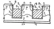
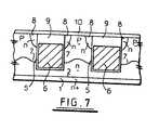
- FIG. 7is a schematic illustration of a cross-section of part of a n-channel (n p-n) UMOS device which has been fabricated according to the invention.
- a semiconductor bodyis formed on a substrate defining an n+ type semiconductor drain region 1 .
- the semiconductor bodycomprises an n type drain region 2 extending to an upper surface 3 of the semiconductor body which supports a masking layer 4 which may be selectively removed by etching to define areas where trenches are to be formed in the region 2 .
- the drain region 2may be an epitaxial layer.
- the masking layer 4may comprise a single material type, for example silicon dioxide, or it may be a multi-layer comprising several different materials, for example silicon dioxide/silicon nitride/silicon dioxide. After selective removal of the mask 4 , trenches are etched to a predetermined depth through the exposed surface 3 and into region 2 , as shown in FIG. 2, using a known method, for example reactive ion etching.
- the illustrated multi-layer structurewill be formed on a wafer substrate which might he 600 ⁇ m thick.
- the substratein effect forms the drain region 1 of FIG. 1 .
- the layers 2 and 4 built up on the substratewill be very much thinner than the substrate itself.
- the region 2may be 6 ⁇ m thick.
- the layer 1is shown in the Figures as being relatively thin simply for the purposes of illustration.
- An insulating layer 5is formed using a known technique on the walls of the trenches as shown in FIG. 3 .
- One such known techniqueis thermal oxidation.
- Layer 5may also be formed as a composite oxide/nitride layer. Some or all of the layer 5 may comprise deposited material.
- a gate material 6for example polysilicon, is introduced into the trenches, for example using a low pressure chemical vapour deposition technique.
- the polysilicon gate material 6is arranged to partially fill the trenches, as shown in FIG. 4, for example by first filling the trenches and then etching back some of the polysilicon 6 .
- the polysilicon 6may be doped to effect an improvement in conductivity. This may be done during or after deposition.
- aluminium gatesmay be arranged partially to fill the trenches, without requiring to be etched back, using a method described in WO 9700536.
- p-type body dopantis introduced laterally into region 2 through the sidewalls of the trenches.
- the body dopant introduced through the trench sidewallsinitially remains close to those sidewalls.
- the dopantsare then diffused to form p-type body regions 7 .
- the body dopantmay be introduced into the trench sidewalls using charged dopant ions (for example ionic boron) which pass directly through the oxide layer 5 and into the region 2 .
- the ionsmay be directed into the trenches using for example an angled source, divergent source or an isotropic source. More than one implant step may be used to introduce the total body dopant, for instance a separate source for each side of the trenches may be utilised.
- composition and thickness of the trench masking layer 4may be chosen such that some body dopant enters the upper surface of the substrate through the masking layer 4 , as well as laterally through the trench sidewall.
- dopant penetration into the upper surface 3 of the semiconductormay be enhanced by prior partial etching of the masked layer 4 in the vertical direction in order to reduce its thickness.
- one dopantmay be ion implanted at a relatively low energy, such that the mask 4 is not penetrated substantially by the dopant, whereas the other dopant may be implanted at a relatively high energy such that the mask 4 is substantially penetrated by the dopant.
- other known methods of dopant introductionmay be used, for example gaseous predeposition. Some methods may require that the oxide layer 5 is first removed from the walls of the trenches above the gate material.
- the position of the boundary between the body regions and the n-substrate regiondepends upon the distance penetrated by the body dopant within the substrate, and upon the vertical position of an upper surface of the gate material 6 within the trenches.
- the penetration distancecan be closely controlled, and therefore the position of the boundary relative to the upper surface of each gate region 6 is accurately determined.
- source dopantis introduced laterally through the side walls of the trenches, using a technique such as one of those described above, to form source regions 8 .
- the source dopantis implanted through the oxide layer 5 on the trench wall, but it would be possible to remove the outer layer 5 before the introduction of the source dopant.
- the source dopantis prevented from entering at least part of the upper surface of the substrate by those portions of the trench masking layer 4 which have not been removed.
- the diffusion of the source dopantis arranged such that it penetrates to a lesser distance than the body dopant, so that a portion of body region 7 is interposed between each source region 8 and drain region 2 .
- the penetration distance of the source dopantis closely controlled such that the position of the boundary between the regions 7 and 8 relative to the position of the upper surface of each gate region 6 is accurately determined. It will be appreciated that driving in the source regions 7 may cause some further diffusion of the dopant forming the body regions 8 , but this further diffusion can be taken into account when determining the desired relative positions of the source and body region boundaries.
- each gate region 6Since any variation in the vertical position of the upper surface of each gate region 6 affects the vertical penetration distance of both body and source dopants equally, the vertical extent of body region 7 between the sources 8 and the drain region 2 will be substantially the same throughout the lateral area of the substrate. Consequently, the vertical thickness of the portion of body region 7 interposed between a source region 8 and the drain region 2 , known as the channel width, is accurately determined.
- the fabrication methodis completed, as shown in FIG. 7, by isolating the uppermost surface of the etched-back polysilicon gates 6 with an insulating material 9 , and by completely removing the mask 4 to expose the upper surface of the silicon.
- a layer of metal 10is then added to the upper surface of the structure, to form an electrical contact to the source and body regions.
- a shallow p-type implantmay additionally be carried out, after the removal of layer 4 , in order to boost the p-type dopant concentration and thereby improve the electrical contact between the body regions 7 and the metal region 10 .
- the gate regions 6will be connected elsewhere to a gate contact metallisation region.
- p and n type regionsmay be interchanged throughout to arrive at a p-channel (p-n-p) rather than n-channel (n-p-n) structure.
- an additional layer beneath layer 1 and of opposite type to layer 1may be present, resulting in the formation of a n-channel or p-channel IGBT structure.
- the attached drawingsshow the formation of two adjacent trenches. It will be appreciated that the method of the present invention may be applied to a wide variety of trench configurations, for example the formation of a hexagonal array in which trenches are etched in spaces defined between a tightly packed array of hexagonal mesa areas on the surface of a substrate.
- the above-described methodrefers to an embodiment in which the first-introduced dopant forms the body regions 7 and the second-introduced dopant forms the source regions 8 .
- the second-introduced dopantis arranged to penetrate to a final position deeper than the final position of the first-introduced dopant.
- the second-introduced dopantforms the body regions and the first-introduced dopant forms the source regions.
- the advantage of such a methodis that remaining portions of the trench mask 4 can be used to mask the first (source) dopant, but removed before the introduction of the second (body) dopant, such that body dopant enters the upper surface of the semiconductor body as well as the trench sidewalls.
- a further possibilityis to diffuse (drive-in) both dopants simultaneously following an initial introduction of both source and body dopants.
- This approachhas two advantages. Firstly, both body and source dopants are subjected to exactly the same drive-in conditions, so that any unintentional wafer-to-wafer and batch-to-batch variations in manufacturing conditions, e.g. related to furnace operation, are applied to both dopants equally, thereby improving uniformity in the final channel width. Secondly there is an associated reduction in the complexity of the manufacturing process, as separate body and source drives are replaced by a single drive.
- the channel width of a resulting UMOS structureis dependent only on the diffusion distances of the body 7 and source 8 regions, since both are aligned to the same physical feature (i.e. the position of the top of the etched-back gate polysilicon 6 ). Variations in the position of this feature do not alter the relative positions of the body 7 and source 8 , and therefore do not alter the vertical extent of the channel width region between the source 8 and drain region 2 . This allows the vertical extent of the channel to be optimised with greater precision than is possible with prior art fabrication methods.
- junction depthsare determined by the lateral introduction of the body and source dopant ions, which provides for substantially identical and uniform depths of body 7 and source 8 at every position within the device active area, thereby ensuring that the critical ‘channel width’ dimension is substantially uniform across the device active area.
- the present methodrequires no critical mask alignments. This allows a substantial reduction in lateral dimensions within the active area of the UMOS structure, and a corresponding increase in the density of UMOS trench edge per unit area. Regions of p+ doping in the body regions, commonly seen in the prior art, are unnecessary due to the very close spacing of trenches, which spacing is made possible by the absence of critical masking of the source regions.
Landscapes
- Insulated Gate Type Field-Effect Transistor (AREA)
- Junction Field-Effect Transistors (AREA)
Abstract
Description
Claims (20)
Applications Claiming Priority (3)
| Application Number | Priority Date | Filing Date | Title |
|---|---|---|---|
| GB9723468 | 1997-11-07 | ||
| GBGB9723468.6AGB9723468D0 (en) | 1997-11-07 | 1997-11-07 | Method of semiconductor device fabrication |
| PCT/GB1998/003333WO1999025016A1 (en) | 1997-11-07 | 1998-11-06 | Method of semiconductor device fabrication |
Publications (1)
| Publication Number | Publication Date |
|---|---|
| US6376314B1true US6376314B1 (en) | 2002-04-23 |
Family
ID=10821684
Family Applications (1)
| Application Number | Title | Priority Date | Filing Date |
|---|---|---|---|
| US09/530,802Expired - LifetimeUS6376314B1 (en) | 1997-11-07 | 1998-11-06 | Method of semiconductor device fabrication |
Country Status (4)
| Country | Link |
|---|---|
| US (1) | US6376314B1 (en) |
| AU (1) | AU1163399A (en) |
| GB (2) | GB9723468D0 (en) |
| WO (1) | WO1999025016A1 (en) |
Cited By (44)
| Publication number | Priority date | Publication date | Assignee | Title |
|---|---|---|---|---|
| US6583010B2 (en) | 1999-03-31 | 2003-06-24 | Fairchild Semiconductor Corporation | Trench transistor with self-aligned source |
| US20040021173A1 (en)* | 2002-07-30 | 2004-02-05 | Fairchild Semiconductor Corporation | Dual trench power mosfet |
| US6710418B1 (en) | 2002-10-11 | 2004-03-23 | Fairchild Semiconductor Corporation | Schottky rectifier with insulation-filled trenches and method of forming the same |
| US6713813B2 (en) | 2001-01-30 | 2004-03-30 | Fairchild Semiconductor Corporation | Field effect transistor having a lateral depletion structure |
| US20040065919A1 (en)* | 2002-10-03 | 2004-04-08 | Wilson Peter H. | Trench gate laterally diffused MOSFET devices and methods for making such devices |
| US20040115790A1 (en)* | 2001-02-13 | 2004-06-17 | Tiina Pakula | Method for production of secreted proteins in fungi |
| US20040132252A1 (en)* | 2001-01-30 | 2004-07-08 | Merchant Bruce D. | Method of forming a field effect transistor having a lateral depletion structure |
| US20040142523A1 (en)* | 2000-08-16 | 2004-07-22 | Izak Bencuya | Method of forming vertical mosfet with ultra-low on-resistance and low gate charge |
| US6802719B2 (en)* | 2000-09-09 | 2004-10-12 | Zetex Plc | Implantation method |
| US6803626B2 (en) | 2002-07-18 | 2004-10-12 | Fairchild Semiconductor Corporation | Vertical charge control semiconductor device |
| US20040232479A1 (en)* | 2001-04-11 | 2004-11-25 | Baliga Bantval Jayant | Methods of forming vertical power devices having trench-based source electrodes with sidewall source contacts |
| US20040232481A1 (en)* | 2003-05-20 | 2004-11-25 | Robert Herrick | Structure and method for forming a trench MOSFET having self-aligned features |
| US20040256690A1 (en)* | 2001-10-17 | 2004-12-23 | Kocon Christopher Boguslaw | Schottky diode using charge balance structure |
| US20050116313A1 (en)* | 2003-11-28 | 2005-06-02 | Lee Jae-Gil | Superjunction semiconductor device |
| US20050153497A1 (en)* | 2000-08-16 | 2005-07-14 | Izak Bencuya | Method of forming a FET having ultra-low on-resistance and low gate charge |
| US20050199918A1 (en)* | 2004-03-15 | 2005-09-15 | Daniel Calafut | Optimized trench power MOSFET with integrated schottky diode |
| US6991977B2 (en) | 2001-10-17 | 2006-01-31 | Fairchild Semiconductor Corporation | Method for forming a semiconductor structure with improved smaller forward voltage loss and higher blocking capability |
| US20060134867A1 (en)* | 2003-05-29 | 2006-06-22 | Third Dimension (3D) Semiconductor, Inc. | Technique for forming the deep doped columns in superjunction |
| US7078296B2 (en) | 2002-01-16 | 2006-07-18 | Fairchild Semiconductor Corporation | Self-aligned trench MOSFETs and methods for making the same |
| US20060214222A1 (en)* | 2003-05-20 | 2006-09-28 | Ashok Challa | Power semiconductor devices and methods of manufacture |
| US7132712B2 (en) | 2002-11-05 | 2006-11-07 | Fairchild Semiconductor Corporation | Trench structure having one or more diodes embedded therein adjacent a PN junction |
| US7265416B2 (en) | 2002-02-23 | 2007-09-04 | Fairchild Korea Semiconductor Ltd. | High breakdown voltage low on-resistance lateral DMOS transistor |
| US7265415B2 (en) | 2004-10-08 | 2007-09-04 | Fairchild Semiconductor Corporation | MOS-gated transistor with reduced miller capacitance |
| US7319256B1 (en) | 2006-06-19 | 2008-01-15 | Fairchild Semiconductor Corporation | Shielded gate trench FET with the shield and gate electrodes being connected together |
| US7345342B2 (en) | 2001-01-30 | 2008-03-18 | Fairchild Semiconductor Corporation | Power semiconductor devices and methods of manufacture |
| US7352036B2 (en) | 2004-08-03 | 2008-04-01 | Fairchild Semiconductor Corporation | Semiconductor power device having a top-side drain using a sinker trench |
| US20080079112A1 (en)* | 2006-09-28 | 2008-04-03 | Elpida Memory, Inc. | Semiconductor device and manufacturing method thereof |
| US7368777B2 (en) | 2003-12-30 | 2008-05-06 | Fairchild Semiconductor Corporation | Accumulation device with charge balance structure and method of forming the same |
| US7385248B2 (en) | 2005-08-09 | 2008-06-10 | Fairchild Semiconductor Corporation | Shielded gate field effect transistor with improved inter-poly dielectric |
| US7446374B2 (en) | 2006-03-24 | 2008-11-04 | Fairchild Semiconductor Corporation | High density trench FET with integrated Schottky diode and method of manufacture |
| US7504306B2 (en) | 2005-04-06 | 2009-03-17 | Fairchild Semiconductor Corporation | Method of forming trench gate field effect transistor with recessed mesas |
| US7576388B1 (en) | 2002-10-03 | 2009-08-18 | Fairchild Semiconductor Corporation | Trench-gate LDMOS structures |
| US7625793B2 (en) | 1999-12-20 | 2009-12-01 | Fairchild Semiconductor Corporation | Power MOS device with improved gate charge performance |
| US7772668B2 (en) | 2007-12-26 | 2010-08-10 | Fairchild Semiconductor Corporation | Shielded gate trench FET with multiple channels |
| US20120018793A1 (en)* | 2007-04-30 | 2012-01-26 | Anup Bhalla | Device structure and manufacturing method using HDP deposited using deposited source-body implant block |
| US20120276701A1 (en)* | 2011-04-27 | 2012-11-01 | Yedinak Joseph A | Superjunction Structures for Power Devices and Methods of Manufacture |
| US8319290B2 (en) | 2010-06-18 | 2012-11-27 | Fairchild Semiconductor Corporation | Trench MOS barrier schottky rectifier with a planar surface using CMP techniques |
| US8592895B2 (en) | 2005-06-10 | 2013-11-26 | Fairchild Semiconductor Corporation | Field effect transistor with source, heavy body region and shielded gate |
| US8772868B2 (en) | 2011-04-27 | 2014-07-08 | Fairchild Semiconductor Corporation | Superjunction structures for power devices and methods of manufacture |
| US8786010B2 (en) | 2011-04-27 | 2014-07-22 | Fairchild Semiconductor Corporation | Superjunction structures for power devices and methods of manufacture |
| US8836028B2 (en) | 2011-04-27 | 2014-09-16 | Fairchild Semiconductor Corporation | Superjunction structures for power devices and methods of manufacture |
| US8928077B2 (en) | 2007-09-21 | 2015-01-06 | Fairchild Semiconductor Corporation | Superjunction structures for power devices |
| US9431481B2 (en) | 2008-09-19 | 2016-08-30 | Fairchild Semiconductor Corporation | Superjunction structures for power devices and methods of manufacture |
| US9553185B2 (en) | 2010-05-27 | 2017-01-24 | Fuji Electric Co., Ltd. | MOS-driven semiconductor device and method for manufacturing MOS-driven semiconductor device |
Families Citing this family (1)
| Publication number | Priority date | Publication date | Assignee | Title |
|---|---|---|---|---|
| JP2002110978A (en)* | 2000-10-02 | 2002-04-12 | Toshiba Corp | Power semiconductor device |
Citations (9)
| Publication number | Priority date | Publication date | Assignee | Title |
|---|---|---|---|---|
| FR2647596A1 (en) | 1989-05-24 | 1990-11-30 | Fuji Electric Co Ltd | ISOLATED GRID FIELD EFFECT TRANSISTOR AND METHOD FOR MANUFACTURING THE SAME |
| US5156985A (en)* | 1990-05-08 | 1992-10-20 | Matsushita Electric Industrial Co., Ltd. | Method for making a charge transfer semiconductor device having an oblong trench |
| GB2286082A (en) | 1994-01-19 | 1995-08-02 | Hyundai Electronics Ind | Semiconductor device having a trench structure |
| US5578508A (en) | 1993-10-28 | 1996-11-26 | Kabushiki Kaisha Toshiba | Vertical power MOSFET and process of fabricating the same |
| WO1997000536A1 (en) | 1995-06-14 | 1997-01-03 | Totem Semiconductor Ltd | Semiconductor device fabrication |
| US5652152A (en) | 1996-04-22 | 1997-07-29 | Chartered Semiconductor Manufacturing Pte, Ltd. | Process having high tolerance to buried contact mask misalignment by using a PSG spacer |
| US5915195A (en)* | 1997-11-25 | 1999-06-22 | Advanced Micro Devices, Inc. | Ion implantation process to improve the gate oxide quality at the edge of a shallow trench isolation structure |
| US6051468A (en)* | 1997-09-15 | 2000-04-18 | Magepower Semiconductor Corp. | Method of forming a semiconductor structure with uniform threshold voltage and punch-through tolerance |
| US6103578A (en)* | 1997-02-10 | 2000-08-15 | Mitsubishi Denki Kabushiki Kaisha | Method for forming high breakdown semiconductor device |
- 1997
- 1997-11-07GBGBGB9723468.6Apatent/GB9723468D0/ennot_activeCeased
- 1998
- 1998-11-06WOPCT/GB1998/003333patent/WO1999025016A1/enactiveApplication Filing
- 1998-11-06GBGB0010867Apatent/GB2347268B/ennot_activeExpired - Fee Related
- 1998-11-06USUS09/530,802patent/US6376314B1/ennot_activeExpired - Lifetime
- 1998-11-06AUAU11633/99Apatent/AU1163399A/ennot_activeAbandoned
Patent Citations (10)
| Publication number | Priority date | Publication date | Assignee | Title |
|---|---|---|---|---|
| FR2647596A1 (en) | 1989-05-24 | 1990-11-30 | Fuji Electric Co Ltd | ISOLATED GRID FIELD EFFECT TRANSISTOR AND METHOD FOR MANUFACTURING THE SAME |
| US5086007A (en)* | 1989-05-24 | 1992-02-04 | Fuji Electric Co., Ltd. | Method of manufacturing an insulated gate field effect transistor |
| US5156985A (en)* | 1990-05-08 | 1992-10-20 | Matsushita Electric Industrial Co., Ltd. | Method for making a charge transfer semiconductor device having an oblong trench |
| US5578508A (en) | 1993-10-28 | 1996-11-26 | Kabushiki Kaisha Toshiba | Vertical power MOSFET and process of fabricating the same |
| GB2286082A (en) | 1994-01-19 | 1995-08-02 | Hyundai Electronics Ind | Semiconductor device having a trench structure |
| WO1997000536A1 (en) | 1995-06-14 | 1997-01-03 | Totem Semiconductor Ltd | Semiconductor device fabrication |
| US5652152A (en) | 1996-04-22 | 1997-07-29 | Chartered Semiconductor Manufacturing Pte, Ltd. | Process having high tolerance to buried contact mask misalignment by using a PSG spacer |
| US6103578A (en)* | 1997-02-10 | 2000-08-15 | Mitsubishi Denki Kabushiki Kaisha | Method for forming high breakdown semiconductor device |
| US6051468A (en)* | 1997-09-15 | 2000-04-18 | Magepower Semiconductor Corp. | Method of forming a semiconductor structure with uniform threshold voltage and punch-through tolerance |
| US5915195A (en)* | 1997-11-25 | 1999-06-22 | Advanced Micro Devices, Inc. | Ion implantation process to improve the gate oxide quality at the edge of a shallow trench isolation structure |
Cited By (110)
| Publication number | Priority date | Publication date | Assignee | Title |
|---|---|---|---|---|
| US6583010B2 (en) | 1999-03-31 | 2003-06-24 | Fairchild Semiconductor Corporation | Trench transistor with self-aligned source |
| US7625793B2 (en) | 1999-12-20 | 2009-12-01 | Fairchild Semiconductor Corporation | Power MOS device with improved gate charge performance |
| US20040142523A1 (en)* | 2000-08-16 | 2004-07-22 | Izak Bencuya | Method of forming vertical mosfet with ultra-low on-resistance and low gate charge |
| US7745289B2 (en) | 2000-08-16 | 2010-06-29 | Fairchild Semiconductor Corporation | Method of forming a FET having ultra-low on-resistance and low gate charge |
| US20100258864A1 (en)* | 2000-08-16 | 2010-10-14 | Izak Bencuya | Method of Forming a FET Having Ultra-low On-resistance and Low Gate Charge |
| US8101484B2 (en) | 2000-08-16 | 2012-01-24 | Fairchild Semiconductor Corporation | Method of forming a FET having ultra-low on-resistance and low gate charge |
| US20050153497A1 (en)* | 2000-08-16 | 2005-07-14 | Izak Bencuya | Method of forming a FET having ultra-low on-resistance and low gate charge |
| US8710584B2 (en) | 2000-08-16 | 2014-04-29 | Fairchild Semiconductor Corporation | FET device having ultra-low on-resistance and low gate charge |
| US6802719B2 (en)* | 2000-09-09 | 2004-10-12 | Zetex Plc | Implantation method |
| US7345342B2 (en) | 2001-01-30 | 2008-03-18 | Fairchild Semiconductor Corporation | Power semiconductor devices and methods of manufacture |
| US6818513B2 (en) | 2001-01-30 | 2004-11-16 | Fairchild Semiconductor Corporation | Method of forming a field effect transistor having a lateral depletion structure |
| US9368587B2 (en) | 2001-01-30 | 2016-06-14 | Fairchild Semiconductor Corporation | Accumulation-mode field effect transistor with improved current capability |
| US6713813B2 (en) | 2001-01-30 | 2004-03-30 | Fairchild Semiconductor Corporation | Field effect transistor having a lateral depletion structure |
| US20110014764A1 (en)* | 2001-01-30 | 2011-01-20 | Marchant Bruce D | Method of forming a dual-trench field effect transistor |
| US20050029618A1 (en)* | 2001-01-30 | 2005-02-10 | Marchant Bruce D. | Structure and method of forming a dual-trench field effect transistor |
| US8829641B2 (en) | 2001-01-30 | 2014-09-09 | Fairchild Semiconductor Corporation | Method of forming a dual-trench field effect transistor |
| US20040132252A1 (en)* | 2001-01-30 | 2004-07-08 | Merchant Bruce D. | Method of forming a field effect transistor having a lateral depletion structure |
| US20040115790A1 (en)* | 2001-02-13 | 2004-06-17 | Tiina Pakula | Method for production of secreted proteins in fungi |
| US20040232479A1 (en)* | 2001-04-11 | 2004-11-25 | Baliga Bantval Jayant | Methods of forming vertical power devices having trench-based source electrodes with sidewall source contacts |
| US7061066B2 (en) | 2001-10-17 | 2006-06-13 | Fairchild Semiconductor Corporation | Schottky diode using charge balance structure |
| US6991977B2 (en) | 2001-10-17 | 2006-01-31 | Fairchild Semiconductor Corporation | Method for forming a semiconductor structure with improved smaller forward voltage loss and higher blocking capability |
| US7429523B2 (en) | 2001-10-17 | 2008-09-30 | Fairchild Semiconductor Corporation | Method of forming schottky diode with charge balance structure |
| US20040256690A1 (en)* | 2001-10-17 | 2004-12-23 | Kocon Christopher Boguslaw | Schottky diode using charge balance structure |
| US7078296B2 (en) | 2002-01-16 | 2006-07-18 | Fairchild Semiconductor Corporation | Self-aligned trench MOSFETs and methods for making the same |
| US7605040B2 (en) | 2002-02-23 | 2009-10-20 | Fairchild Korea Semiconductor Ltd. | Method of forming high breakdown voltage low on-resistance lateral DMOS transistor |
| US7265416B2 (en) | 2002-02-23 | 2007-09-04 | Fairchild Korea Semiconductor Ltd. | High breakdown voltage low on-resistance lateral DMOS transistor |
| US7291894B2 (en) | 2002-07-18 | 2007-11-06 | Fairchild Semiconductor Corporation | Vertical charge control semiconductor device with low output capacitance |
| US6803626B2 (en) | 2002-07-18 | 2004-10-12 | Fairchild Semiconductor Corporation | Vertical charge control semiconductor device |
| US7977744B2 (en) | 2002-07-18 | 2011-07-12 | Fairchild Semiconductor Corporation | Field effect transistor with trench filled with insulating material and strips of semi-insulating material along trench sidewalls |
| US20050023607A1 (en)* | 2002-07-18 | 2005-02-03 | Steven Sapp | Vertical charge control semiconductor device with low output capacitance |
| US6710403B2 (en) | 2002-07-30 | 2004-03-23 | Fairchild Semiconductor Corporation | Dual trench power MOSFET |
| US20040021173A1 (en)* | 2002-07-30 | 2004-02-05 | Fairchild Semiconductor Corporation | Dual trench power mosfet |
| US8198677B2 (en) | 2002-10-03 | 2012-06-12 | Fairchild Semiconductor Corporation | Trench-gate LDMOS structures |
| US20040065919A1 (en)* | 2002-10-03 | 2004-04-08 | Wilson Peter H. | Trench gate laterally diffused MOSFET devices and methods for making such devices |
| US7033891B2 (en) | 2002-10-03 | 2006-04-25 | Fairchild Semiconductor Corporation | Trench gate laterally diffused MOSFET devices and methods for making such devices |
| US7576388B1 (en) | 2002-10-03 | 2009-08-18 | Fairchild Semiconductor Corporation | Trench-gate LDMOS structures |
| US6710418B1 (en) | 2002-10-11 | 2004-03-23 | Fairchild Semiconductor Corporation | Schottky rectifier with insulation-filled trenches and method of forming the same |
| US7132712B2 (en) | 2002-11-05 | 2006-11-07 | Fairchild Semiconductor Corporation | Trench structure having one or more diodes embedded therein adjacent a PN junction |
| US7582519B2 (en) | 2002-11-05 | 2009-09-01 | Fairchild Semiconductor Corporation | Method of forming a trench structure having one or more diodes embedded therein adjacent a PN junction |
| US7638841B2 (en) | 2003-05-20 | 2009-12-29 | Fairchild Semiconductor Corporation | Power semiconductor devices and methods of manufacture |
| US8143123B2 (en) | 2003-05-20 | 2012-03-27 | Fairchild Semiconductor Corporation | Methods of forming inter-poly dielectric (IPD) layers in power semiconductor devices |
| US20080164519A1 (en)* | 2003-05-20 | 2008-07-10 | Robert Herrick | Power Device with Trenches Having Wider Upper Portion than Lower Portion |
| US20040232481A1 (en)* | 2003-05-20 | 2004-11-25 | Robert Herrick | Structure and method for forming a trench MOSFET having self-aligned features |
| US8936985B2 (en) | 2003-05-20 | 2015-01-20 | Fairchild Semiconductor Corporation | Methods related to power semiconductor devices with thick bottom oxide layers |
| US7855415B2 (en) | 2003-05-20 | 2010-12-21 | Fairchild Semiconductor Corporation | Power semiconductor devices having termination structures and methods of manufacture |
| US20060214222A1 (en)* | 2003-05-20 | 2006-09-28 | Ashok Challa | Power semiconductor devices and methods of manufacture |
| US8889511B2 (en) | 2003-05-20 | 2014-11-18 | Fairchild Semiconductor Corporation | Methods of manufacturing power semiconductor devices with trenched shielded split gate transistor |
| US8786045B2 (en) | 2003-05-20 | 2014-07-22 | Fairchild Semiconductor Corporation | Power semiconductor devices having termination structures |
| US8716783B2 (en) | 2003-05-20 | 2014-05-06 | Fairchild Semiconductor Corporation | Power device with self-aligned source regions |
| US6916745B2 (en) | 2003-05-20 | 2005-07-12 | Fairchild Semiconductor Corporation | Structure and method for forming a trench MOSFET having self-aligned features |
| US7595524B2 (en) | 2003-05-20 | 2009-09-29 | Fairchild Semiconductor Corporation | Power device with trenches having wider upper portion than lower portion |
| US8350317B2 (en) | 2003-05-20 | 2013-01-08 | Fairchild Semiconductor Corporation | Power semiconductor devices and methods of manufacture |
| US20110003449A1 (en)* | 2003-05-20 | 2011-01-06 | Robert Herrick | Power Device With Trenches Having Wider Upper Portion Than Lower Portion |
| US8143124B2 (en) | 2003-05-20 | 2012-03-27 | Fairchild Semiconductor Corporation | Methods of making power semiconductor devices with thick bottom oxide layer |
| US7344943B2 (en) | 2003-05-20 | 2008-03-18 | Fairchild Semiconductor Corporation | Method for forming a trench MOSFET having self-aligned features |
| US20100015769A1 (en)* | 2003-05-20 | 2010-01-21 | Robert Herrick | Power Device With Trenches Having Wider Upper Portion Than Lower Portion |
| US7652326B2 (en) | 2003-05-20 | 2010-01-26 | Fairchild Semiconductor Corporation | Power semiconductor devices and methods of manufacture |
| US8129245B2 (en) | 2003-05-20 | 2012-03-06 | Fairchild Semiconductor Corporation | Methods of manufacturing power semiconductor devices with shield and gate contacts |
| US7982265B2 (en) | 2003-05-20 | 2011-07-19 | Fairchild Semiconductor Corporation | Trenched shield gate power semiconductor devices and methods of manufacture |
| US8034682B2 (en) | 2003-05-20 | 2011-10-11 | Fairchild Semiconductor Corporation | Power device with trenches having wider upper portion than lower portion |
| US8013391B2 (en) | 2003-05-20 | 2011-09-06 | Fairchild Semiconductor Corporation | Power semiconductor devices with trenched shielded split gate transistor and methods of manufacture |
| US8013387B2 (en) | 2003-05-20 | 2011-09-06 | Fairchild Semiconductor Corporation | Power semiconductor devices with shield and gate contacts and methods of manufacture |
| US7799636B2 (en) | 2003-05-20 | 2010-09-21 | Fairchild Semiconductor Corporation | Power device with trenches having wider upper portion than lower portion |
| US20060134867A1 (en)* | 2003-05-29 | 2006-06-22 | Third Dimension (3D) Semiconductor, Inc. | Technique for forming the deep doped columns in superjunction |
| US7504305B2 (en)* | 2003-05-29 | 2009-03-17 | Third Dimension (3D) Semiconductor, Inc. | Technique for forming the deep doped regions in superjunction devices |
| US20090023260A9 (en)* | 2003-05-29 | 2009-01-22 | Third Dimension (3D) Semiconductor, Inc. | Technique for forming the deep doped columns in superjunction |
| US7655981B2 (en) | 2003-11-28 | 2010-02-02 | Fairchild Korea Semiconductor Ltd. | Superjunction semiconductor device |
| US7301203B2 (en) | 2003-11-28 | 2007-11-27 | Fairchild Korea Semiconductor Ltd. | Superjunction semiconductor device |
| US20080211053A1 (en)* | 2003-11-28 | 2008-09-04 | Fairchild Korea Semiconductor Ltd. | Superjunction Semiconductor Device |
| US20050116313A1 (en)* | 2003-11-28 | 2005-06-02 | Lee Jae-Gil | Superjunction semiconductor device |
| US7368777B2 (en) | 2003-12-30 | 2008-05-06 | Fairchild Semiconductor Corporation | Accumulation device with charge balance structure and method of forming the same |
| US7936008B2 (en) | 2003-12-30 | 2011-05-03 | Fairchild Semiconductor Corporation | Structure and method for forming accumulation-mode field effect transistor with improved current capability |
| US8518777B2 (en) | 2003-12-30 | 2013-08-27 | Fairchild Semiconductor Corporation | Method for forming accumulation-mode field effect transistor with improved current capability |
| US20050199918A1 (en)* | 2004-03-15 | 2005-09-15 | Daniel Calafut | Optimized trench power MOSFET with integrated schottky diode |
| US8026558B2 (en) | 2004-08-03 | 2011-09-27 | Fairchild Semiconductor Corporation | Semiconductor power device having a top-side drain using a sinker trench |
| US7732876B2 (en) | 2004-08-03 | 2010-06-08 | Fairchild Semiconductor Corporation | Power transistor with trench sinker for contacting the backside |
| US8148233B2 (en) | 2004-08-03 | 2012-04-03 | Fairchild Semiconductor Corporation | Semiconductor power device having a top-side drain using a sinker trench |
| US7352036B2 (en) | 2004-08-03 | 2008-04-01 | Fairchild Semiconductor Corporation | Semiconductor power device having a top-side drain using a sinker trench |
| US7534683B2 (en) | 2004-10-08 | 2009-05-19 | Fairchild Semiconductor Corporation | Method of making a MOS-gated transistor with reduced miller capacitance |
| US7265415B2 (en) | 2004-10-08 | 2007-09-04 | Fairchild Semiconductor Corporation | MOS-gated transistor with reduced miller capacitance |
| US8084327B2 (en) | 2005-04-06 | 2011-12-27 | Fairchild Semiconductor Corporation | Method for forming trench gate field effect transistor with recessed mesas using spacers |
| US8680611B2 (en) | 2005-04-06 | 2014-03-25 | Fairchild Semiconductor Corporation | Field effect transistor and schottky diode structures |
| US7504306B2 (en) | 2005-04-06 | 2009-03-17 | Fairchild Semiconductor Corporation | Method of forming trench gate field effect transistor with recessed mesas |
| US8592895B2 (en) | 2005-06-10 | 2013-11-26 | Fairchild Semiconductor Corporation | Field effect transistor with source, heavy body region and shielded gate |
| US7598144B2 (en) | 2005-08-09 | 2009-10-06 | Fairchild Semiconductor Corporation | Method for forming inter-poly dielectric in shielded gate field effect transistor |
| US7385248B2 (en) | 2005-08-09 | 2008-06-10 | Fairchild Semiconductor Corporation | Shielded gate field effect transistor with improved inter-poly dielectric |
| US7713822B2 (en) | 2006-03-24 | 2010-05-11 | Fairchild Semiconductor Corporation | Method of forming high density trench FET with integrated Schottky diode |
| US7446374B2 (en) | 2006-03-24 | 2008-11-04 | Fairchild Semiconductor Corporation | High density trench FET with integrated Schottky diode and method of manufacture |
| US7859047B2 (en) | 2006-06-19 | 2010-12-28 | Fairchild Semiconductor Corporation | Shielded gate trench FET with the shield and gate electrodes connected together in non-active region |
| US7473603B2 (en) | 2006-06-19 | 2009-01-06 | Fairchild Semiconductor Corporation | Method for forming a shielded gate trench FET with the shield and gate electrodes being connected together |
| US7319256B1 (en) | 2006-06-19 | 2008-01-15 | Fairchild Semiconductor Corporation | Shielded gate trench FET with the shield and gate electrodes being connected together |
| US20080079112A1 (en)* | 2006-09-28 | 2008-04-03 | Elpida Memory, Inc. | Semiconductor device and manufacturing method thereof |
| US7897459B2 (en)* | 2006-09-28 | 2011-03-01 | Elpida Memory, Inc. | Semiconductor device and manufacturing method thereof |
| US8372708B2 (en)* | 2007-04-30 | 2013-02-12 | Anup Bhalla | Device structure and manufacturing method using HDP deposited using deposited source-body implant block |
| US20120018793A1 (en)* | 2007-04-30 | 2012-01-26 | Anup Bhalla | Device structure and manufacturing method using HDP deposited using deposited source-body implant block |
| US9595596B2 (en) | 2007-09-21 | 2017-03-14 | Fairchild Semiconductor Corporation | Superjunction structures for power devices |
| US8928077B2 (en) | 2007-09-21 | 2015-01-06 | Fairchild Semiconductor Corporation | Superjunction structures for power devices |
| US7772668B2 (en) | 2007-12-26 | 2010-08-10 | Fairchild Semiconductor Corporation | Shielded gate trench FET with multiple channels |
| US20100258866A1 (en)* | 2007-12-26 | 2010-10-14 | James Pan | Method for Forming Shielded Gate Trench FET with Multiple Channels |
| US9224853B2 (en) | 2007-12-26 | 2015-12-29 | Fairchild Semiconductor Corporation | Shielded gate trench FET with multiple channels |
| US9431481B2 (en) | 2008-09-19 | 2016-08-30 | Fairchild Semiconductor Corporation | Superjunction structures for power devices and methods of manufacture |
| US9553185B2 (en) | 2010-05-27 | 2017-01-24 | Fuji Electric Co., Ltd. | MOS-driven semiconductor device and method for manufacturing MOS-driven semiconductor device |
| US9818845B2 (en) | 2010-05-27 | 2017-11-14 | Fuji Electric Co., Ltd. | MOS-driven semiconductor device and method for manufacturing MOS-driven semiconductor device |
| US8432000B2 (en) | 2010-06-18 | 2013-04-30 | Fairchild Semiconductor Corporation | Trench MOS barrier schottky rectifier with a planar surface using CMP techniques |
| US8319290B2 (en) | 2010-06-18 | 2012-11-27 | Fairchild Semiconductor Corporation | Trench MOS barrier schottky rectifier with a planar surface using CMP techniques |
| US8836028B2 (en) | 2011-04-27 | 2014-09-16 | Fairchild Semiconductor Corporation | Superjunction structures for power devices and methods of manufacture |
| US8786010B2 (en) | 2011-04-27 | 2014-07-22 | Fairchild Semiconductor Corporation | Superjunction structures for power devices and methods of manufacture |
| US20120276701A1 (en)* | 2011-04-27 | 2012-11-01 | Yedinak Joseph A | Superjunction Structures for Power Devices and Methods of Manufacture |
| US8772868B2 (en) | 2011-04-27 | 2014-07-08 | Fairchild Semiconductor Corporation | Superjunction structures for power devices and methods of manufacture |
| US8673700B2 (en)* | 2011-04-27 | 2014-03-18 | Fairchild Semiconductor Corporation | Superjunction structures for power devices and methods of manufacture |
Also Published As
| Publication number | Publication date |
|---|---|
| GB9723468D0 (en) | 1998-01-07 |
| GB2347268B (en) | 2002-08-14 |
| AU1163399A (en) | 1999-05-31 |
| GB0010867D0 (en) | 2000-06-28 |
| GB2347268A (en) | 2000-08-30 |
| WO1999025016A1 (en) | 1999-05-20 |
Similar Documents
| Publication | Publication Date | Title |
|---|---|---|
| US6376314B1 (en) | Method of semiconductor device fabrication | |
| JP4833517B2 (en) | Method of manufacturing a high voltage power MOSFET having a voltage sustaining region including a doped column formed by rapid diffusion | |
| JP4786872B2 (en) | Power semiconductor devices having voltage sustaining regions including doped columns formed by a single ion implantation process and methods for their manufacture | |
| EP1393362B1 (en) | Method of manufacturing a trench-gate semiconductor device | |
| JP4743744B2 (en) | Semiconductor power device having a floating island voltage sustaining layer | |
| US7067376B2 (en) | High voltage power MOSFET having low on-resistance | |
| US6992350B2 (en) | High voltage power MOSFET having low on-resistance | |
| EP0885460B1 (en) | Trenched dmos transistor with lightly doped tub | |
| US7091552B2 (en) | High voltage power MOSFET having a voltage sustaining region that includes doped columns formed by trench etching and ion implantation | |
| US6750104B2 (en) | High voltage power MOSFET having a voltage sustaining region that includes doped columns formed by trench etching using an etchant gas that is also a doping source | |
| KR100916818B1 (en) | Power semiconductor device and method of forming the device | |
| EP3651202B1 (en) | Semiconductor device with superjunction and oxygen inserted si-layers | |
| JP2008546216A (en) | Charge balanced field effect transistor | |
| JP2005286328A (en) | Process for producing termination region of trench MIS device, semiconductor die including MIS device, and method of forming the same | |
| US6509607B1 (en) | Semiconductor device with reduced source diffusion distance and method of making same | |
| EP4231361B1 (en) | Method for auto-aligned manufacturing of a trench-gate mos transistor, and shielded-gate mos transistor | |
| KR100880872B1 (en) | Methods of forming double diffusion field effect transistors with reduced conduction-resistance and such double diffusion field effect transistors | |
| US6878997B2 (en) | Compensation component and method for fabricating the component |
Legal Events
| Date | Code | Title | Description |
|---|---|---|---|
| AS | Assignment | Owner name:ZETEX PLC, GREAT BRITAIN Free format text:ASSIGNMENT OF ASSIGNORS INTEREST;ASSIGNOR:JERRED, PAUL ANTONY;REEL/FRAME:010929/0530 Effective date:20000605 | |
| FEPP | Fee payment procedure | Free format text:PAYOR NUMBER ASSIGNED (ORIGINAL EVENT CODE: ASPN); ENTITY STATUS OF PATENT OWNER: LARGE ENTITY | |
| STCF | Information on status: patent grant | Free format text:PATENTED CASE | |
| FPAY | Fee payment | Year of fee payment:4 | |
| FPAY | Fee payment | Year of fee payment:8 | |
| FEPP | Fee payment procedure | Free format text:PAYER NUMBER DE-ASSIGNED (ORIGINAL EVENT CODE: RMPN); ENTITY STATUS OF PATENT OWNER: LARGE ENTITY Free format text:PAYOR NUMBER ASSIGNED (ORIGINAL EVENT CODE: ASPN); ENTITY STATUS OF PATENT OWNER: LARGE ENTITY | |
| AS | Assignment | Owner name:BANK OF AMERICA, N.A., AS SECURITY TRUSTEE, TEXAS Free format text:SECURITY AGREEMENT;ASSIGNOR:DIODES ZETEX LIMITED, AS COMPANY;REEL/FRAME:029594/0679 Effective date:20130108 | |
| FPAY | Fee payment | Year of fee payment:12 |