US6375749B1 - Susceptorless semiconductor wafer support and reactor system for epitaxial layer growth - Google Patents
Susceptorless semiconductor wafer support and reactor system for epitaxial layer growthDownload PDFInfo
- Publication number
- US6375749B1 US6375749B1US09/567,659US56765900AUS6375749B1US 6375749 B1US6375749 B1US 6375749B1US 56765900 AUS56765900 AUS 56765900AUS 6375749 B1US6375749 B1US 6375749B1
- Authority
- US
- United States
- Prior art keywords
- wafer
- support device
- contact
- wafer support
- contact member
- Prior art date
- Legal status (The legal status is an assumption and is not a legal conclusion. Google has not performed a legal analysis and makes no representation as to the accuracy of the status listed.)
- Expired - Fee Related
Links
Images


Classifications
- C—CHEMISTRY; METALLURGY
- C23—COATING METALLIC MATERIAL; COATING MATERIAL WITH METALLIC MATERIAL; CHEMICAL SURFACE TREATMENT; DIFFUSION TREATMENT OF METALLIC MATERIAL; COATING BY VACUUM EVAPORATION, BY SPUTTERING, BY ION IMPLANTATION OR BY CHEMICAL VAPOUR DEPOSITION, IN GENERAL; INHIBITING CORROSION OF METALLIC MATERIAL OR INCRUSTATION IN GENERAL
- C23C—COATING METALLIC MATERIAL; COATING MATERIAL WITH METALLIC MATERIAL; SURFACE TREATMENT OF METALLIC MATERIAL BY DIFFUSION INTO THE SURFACE, BY CHEMICAL CONVERSION OR SUBSTITUTION; COATING BY VACUUM EVAPORATION, BY SPUTTERING, BY ION IMPLANTATION OR BY CHEMICAL VAPOUR DEPOSITION, IN GENERAL
- C23C16/00—Chemical coating by decomposition of gaseous compounds, without leaving reaction products of surface material in the coating, i.e. chemical vapour deposition [CVD] processes
- C23C16/44—Chemical coating by decomposition of gaseous compounds, without leaving reaction products of surface material in the coating, i.e. chemical vapour deposition [CVD] processes characterised by the method of coating
- C23C16/455—Chemical coating by decomposition of gaseous compounds, without leaving reaction products of surface material in the coating, i.e. chemical vapour deposition [CVD] processes characterised by the method of coating characterised by the method used for introducing gases into reaction chamber or for modifying gas flows in reaction chamber
- C—CHEMISTRY; METALLURGY
- C23—COATING METALLIC MATERIAL; COATING MATERIAL WITH METALLIC MATERIAL; CHEMICAL SURFACE TREATMENT; DIFFUSION TREATMENT OF METALLIC MATERIAL; COATING BY VACUUM EVAPORATION, BY SPUTTERING, BY ION IMPLANTATION OR BY CHEMICAL VAPOUR DEPOSITION, IN GENERAL; INHIBITING CORROSION OF METALLIC MATERIAL OR INCRUSTATION IN GENERAL
- C23C—COATING METALLIC MATERIAL; COATING MATERIAL WITH METALLIC MATERIAL; SURFACE TREATMENT OF METALLIC MATERIAL BY DIFFUSION INTO THE SURFACE, BY CHEMICAL CONVERSION OR SUBSTITUTION; COATING BY VACUUM EVAPORATION, BY SPUTTERING, BY ION IMPLANTATION OR BY CHEMICAL VAPOUR DEPOSITION, IN GENERAL
- C23C16/00—Chemical coating by decomposition of gaseous compounds, without leaving reaction products of surface material in the coating, i.e. chemical vapour deposition [CVD] processes
- C23C16/44—Chemical coating by decomposition of gaseous compounds, without leaving reaction products of surface material in the coating, i.e. chemical vapour deposition [CVD] processes characterised by the method of coating
- C23C16/458—Chemical coating by decomposition of gaseous compounds, without leaving reaction products of surface material in the coating, i.e. chemical vapour deposition [CVD] processes characterised by the method of coating characterised by the method used for supporting substrates in the reaction chamber
- C23C16/4582—Rigid and flat substrates, e.g. plates or discs
- C23C16/4583—Rigid and flat substrates, e.g. plates or discs the substrate being supported substantially horizontally
- C23C16/4584—Rigid and flat substrates, e.g. plates or discs the substrate being supported substantially horizontally the substrate being rotated
- C—CHEMISTRY; METALLURGY
- C23—COATING METALLIC MATERIAL; COATING MATERIAL WITH METALLIC MATERIAL; CHEMICAL SURFACE TREATMENT; DIFFUSION TREATMENT OF METALLIC MATERIAL; COATING BY VACUUM EVAPORATION, BY SPUTTERING, BY ION IMPLANTATION OR BY CHEMICAL VAPOUR DEPOSITION, IN GENERAL; INHIBITING CORROSION OF METALLIC MATERIAL OR INCRUSTATION IN GENERAL
- C23C—COATING METALLIC MATERIAL; COATING MATERIAL WITH METALLIC MATERIAL; SURFACE TREATMENT OF METALLIC MATERIAL BY DIFFUSION INTO THE SURFACE, BY CHEMICAL CONVERSION OR SUBSTITUTION; COATING BY VACUUM EVAPORATION, BY SPUTTERING, BY ION IMPLANTATION OR BY CHEMICAL VAPOUR DEPOSITION, IN GENERAL
- C23C16/00—Chemical coating by decomposition of gaseous compounds, without leaving reaction products of surface material in the coating, i.e. chemical vapour deposition [CVD] processes
- C23C16/44—Chemical coating by decomposition of gaseous compounds, without leaving reaction products of surface material in the coating, i.e. chemical vapour deposition [CVD] processes characterised by the method of coating
- C23C16/48—Chemical coating by decomposition of gaseous compounds, without leaving reaction products of surface material in the coating, i.e. chemical vapour deposition [CVD] processes characterised by the method of coating by irradiation, e.g. photolysis, radiolysis, particle radiation
- C23C16/481—Chemical coating by decomposition of gaseous compounds, without leaving reaction products of surface material in the coating, i.e. chemical vapour deposition [CVD] processes characterised by the method of coating by irradiation, e.g. photolysis, radiolysis, particle radiation by radiant heating of the substrate
- C—CHEMISTRY; METALLURGY
- C30—CRYSTAL GROWTH
- C30B—SINGLE-CRYSTAL GROWTH; UNIDIRECTIONAL SOLIDIFICATION OF EUTECTIC MATERIAL OR UNIDIRECTIONAL DEMIXING OF EUTECTOID MATERIAL; REFINING BY ZONE-MELTING OF MATERIAL; PRODUCTION OF A HOMOGENEOUS POLYCRYSTALLINE MATERIAL WITH DEFINED STRUCTURE; SINGLE CRYSTALS OR HOMOGENEOUS POLYCRYSTALLINE MATERIAL WITH DEFINED STRUCTURE; AFTER-TREATMENT OF SINGLE CRYSTALS OR A HOMOGENEOUS POLYCRYSTALLINE MATERIAL WITH DEFINED STRUCTURE; APPARATUS THEREFOR
- C30B25/00—Single-crystal growth by chemical reaction of reactive gases, e.g. chemical vapour-deposition growth
- C30B25/02—Epitaxial-layer growth
- C30B25/12—Substrate holders or susceptors
- C—CHEMISTRY; METALLURGY
- C30—CRYSTAL GROWTH
- C30B—SINGLE-CRYSTAL GROWTH; UNIDIRECTIONAL SOLIDIFICATION OF EUTECTIC MATERIAL OR UNIDIRECTIONAL DEMIXING OF EUTECTOID MATERIAL; REFINING BY ZONE-MELTING OF MATERIAL; PRODUCTION OF A HOMOGENEOUS POLYCRYSTALLINE MATERIAL WITH DEFINED STRUCTURE; SINGLE CRYSTALS OR HOMOGENEOUS POLYCRYSTALLINE MATERIAL WITH DEFINED STRUCTURE; AFTER-TREATMENT OF SINGLE CRYSTALS OR A HOMOGENEOUS POLYCRYSTALLINE MATERIAL WITH DEFINED STRUCTURE; APPARATUS THEREFOR
- C30B31/00—Diffusion or doping processes for single crystals or homogeneous polycrystalline material with defined structure; Apparatus therefor
- C30B31/06—Diffusion or doping processes for single crystals or homogeneous polycrystalline material with defined structure; Apparatus therefor by contacting with diffusion material in the gaseous state
- C30B31/14—Substrate holders or susceptors
- H—ELECTRICITY
- H01—ELECTRIC ELEMENTS
- H01L—SEMICONDUCTOR DEVICES NOT COVERED BY CLASS H10
- H01L21/00—Processes or apparatus adapted for the manufacture or treatment of semiconductor or solid state devices or of parts thereof
- H01L21/67—Apparatus specially adapted for handling semiconductor or electric solid state devices during manufacture or treatment thereof; Apparatus specially adapted for handling wafers during manufacture or treatment of semiconductor or electric solid state devices or components ; Apparatus not specifically provided for elsewhere
- H01L21/683—Apparatus specially adapted for handling semiconductor or electric solid state devices during manufacture or treatment thereof; Apparatus specially adapted for handling wafers during manufacture or treatment of semiconductor or electric solid state devices or components ; Apparatus not specifically provided for elsewhere for supporting or gripping
- H01L21/687—Apparatus specially adapted for handling semiconductor or electric solid state devices during manufacture or treatment thereof; Apparatus specially adapted for handling wafers during manufacture or treatment of semiconductor or electric solid state devices or components ; Apparatus not specifically provided for elsewhere for supporting or gripping using mechanical means, e.g. chucks, clamps or pinches
- H01L21/68714—Apparatus specially adapted for handling semiconductor or electric solid state devices during manufacture or treatment thereof; Apparatus specially adapted for handling wafers during manufacture or treatment of semiconductor or electric solid state devices or components ; Apparatus not specifically provided for elsewhere for supporting or gripping using mechanical means, e.g. chucks, clamps or pinches the wafers being placed on a susceptor, stage or support
- H01L21/68728—Apparatus specially adapted for handling semiconductor or electric solid state devices during manufacture or treatment thereof; Apparatus specially adapted for handling wafers during manufacture or treatment of semiconductor or electric solid state devices or components ; Apparatus not specifically provided for elsewhere for supporting or gripping using mechanical means, e.g. chucks, clamps or pinches the wafers being placed on a susceptor, stage or support characterised by a plurality of separate clamping members, e.g. clamping fingers
- H—ELECTRICITY
- H01—ELECTRIC ELEMENTS
- H01L—SEMICONDUCTOR DEVICES NOT COVERED BY CLASS H10
- H01L21/00—Processes or apparatus adapted for the manufacture or treatment of semiconductor or solid state devices or of parts thereof
- H01L21/67—Apparatus specially adapted for handling semiconductor or electric solid state devices during manufacture or treatment thereof; Apparatus specially adapted for handling wafers during manufacture or treatment of semiconductor or electric solid state devices or components ; Apparatus not specifically provided for elsewhere
- H01L21/683—Apparatus specially adapted for handling semiconductor or electric solid state devices during manufacture or treatment thereof; Apparatus specially adapted for handling wafers during manufacture or treatment of semiconductor or electric solid state devices or components ; Apparatus not specifically provided for elsewhere for supporting or gripping
- H01L21/687—Apparatus specially adapted for handling semiconductor or electric solid state devices during manufacture or treatment thereof; Apparatus specially adapted for handling wafers during manufacture or treatment of semiconductor or electric solid state devices or components ; Apparatus not specifically provided for elsewhere for supporting or gripping using mechanical means, e.g. chucks, clamps or pinches
- H01L21/68714—Apparatus specially adapted for handling semiconductor or electric solid state devices during manufacture or treatment thereof; Apparatus specially adapted for handling wafers during manufacture or treatment of semiconductor or electric solid state devices or components ; Apparatus not specifically provided for elsewhere for supporting or gripping using mechanical means, e.g. chucks, clamps or pinches the wafers being placed on a susceptor, stage or support
- H01L21/68735—Apparatus specially adapted for handling semiconductor or electric solid state devices during manufacture or treatment thereof; Apparatus specially adapted for handling wafers during manufacture or treatment of semiconductor or electric solid state devices or components ; Apparatus not specifically provided for elsewhere for supporting or gripping using mechanical means, e.g. chucks, clamps or pinches the wafers being placed on a susceptor, stage or support characterised by edge profile or support profile
- H—ELECTRICITY
- H01—ELECTRIC ELEMENTS
- H01L—SEMICONDUCTOR DEVICES NOT COVERED BY CLASS H10
- H01L21/00—Processes or apparatus adapted for the manufacture or treatment of semiconductor or solid state devices or of parts thereof
- H01L21/67—Apparatus specially adapted for handling semiconductor or electric solid state devices during manufacture or treatment thereof; Apparatus specially adapted for handling wafers during manufacture or treatment of semiconductor or electric solid state devices or components ; Apparatus not specifically provided for elsewhere
- H01L21/683—Apparatus specially adapted for handling semiconductor or electric solid state devices during manufacture or treatment thereof; Apparatus specially adapted for handling wafers during manufacture or treatment of semiconductor or electric solid state devices or components ; Apparatus not specifically provided for elsewhere for supporting or gripping
- H01L21/687—Apparatus specially adapted for handling semiconductor or electric solid state devices during manufacture or treatment thereof; Apparatus specially adapted for handling wafers during manufacture or treatment of semiconductor or electric solid state devices or components ; Apparatus not specifically provided for elsewhere for supporting or gripping using mechanical means, e.g. chucks, clamps or pinches
- H01L21/68714—Apparatus specially adapted for handling semiconductor or electric solid state devices during manufacture or treatment thereof; Apparatus specially adapted for handling wafers during manufacture or treatment of semiconductor or electric solid state devices or components ; Apparatus not specifically provided for elsewhere for supporting or gripping using mechanical means, e.g. chucks, clamps or pinches the wafers being placed on a susceptor, stage or support
- H01L21/6875—Apparatus specially adapted for handling semiconductor or electric solid state devices during manufacture or treatment thereof; Apparatus specially adapted for handling wafers during manufacture or treatment of semiconductor or electric solid state devices or components ; Apparatus not specifically provided for elsewhere for supporting or gripping using mechanical means, e.g. chucks, clamps or pinches the wafers being placed on a susceptor, stage or support characterised by a plurality of individual support members, e.g. support posts or protrusions
- H—ELECTRICITY
- H01—ELECTRIC ELEMENTS
- H01L—SEMICONDUCTOR DEVICES NOT COVERED BY CLASS H10
- H01L21/00—Processes or apparatus adapted for the manufacture or treatment of semiconductor or solid state devices or of parts thereof
- H01L21/67—Apparatus specially adapted for handling semiconductor or electric solid state devices during manufacture or treatment thereof; Apparatus specially adapted for handling wafers during manufacture or treatment of semiconductor or electric solid state devices or components ; Apparatus not specifically provided for elsewhere
- H01L21/683—Apparatus specially adapted for handling semiconductor or electric solid state devices during manufacture or treatment thereof; Apparatus specially adapted for handling wafers during manufacture or treatment of semiconductor or electric solid state devices or components ; Apparatus not specifically provided for elsewhere for supporting or gripping
- H01L21/687—Apparatus specially adapted for handling semiconductor or electric solid state devices during manufacture or treatment thereof; Apparatus specially adapted for handling wafers during manufacture or treatment of semiconductor or electric solid state devices or components ; Apparatus not specifically provided for elsewhere for supporting or gripping using mechanical means, e.g. chucks, clamps or pinches
- H01L21/68714—Apparatus specially adapted for handling semiconductor or electric solid state devices during manufacture or treatment thereof; Apparatus specially adapted for handling wafers during manufacture or treatment of semiconductor or electric solid state devices or components ; Apparatus not specifically provided for elsewhere for supporting or gripping using mechanical means, e.g. chucks, clamps or pinches the wafers being placed on a susceptor, stage or support
- H01L21/68785—Apparatus specially adapted for handling semiconductor or electric solid state devices during manufacture or treatment thereof; Apparatus specially adapted for handling wafers during manufacture or treatment of semiconductor or electric solid state devices or components ; Apparatus not specifically provided for elsewhere for supporting or gripping using mechanical means, e.g. chucks, clamps or pinches the wafers being placed on a susceptor, stage or support characterised by the mechanical construction of the susceptor, stage or support
Definitions
- the present inventionrelates generally to semiconductor wafer fabrication, and more specifically to a reactor system and wafer support for use during epitaxial growth of a semiconductor material on a semiconductor wafer.
- epilayersIn the semiconductor wafer manufacturing industry, thin epitaxial layers of semiconductor material, such as silicon or gallium arsenide, are grown on a surface of a semiconductor wafer. These epitaxial layers, commonly referred to as epilayers, form the material within which many modern integrated circuits are fabricated. In addition, many other devices, including optoelectric sensors, light emitting diodes, and micromachined mechanical devices, may be fabricated from epilayer material. As epilayers are a fundamental building block for many technologies, is critical that they be manufactured as efficiently and defect-free as possible, to reduce the cost and increase the quality of the epilayer.
- Epilayersmay be grown according to a variety of methods, including molecular beam epitaxy (MBE), vapor phase epitaxy (VPE), and liquid phase epitaxy (LPE).
- MBEmolecular beam epitaxy
- VPEvapor phase epitaxy
- LPEliquid phase epitaxy
- epilayer semiconductor constituentssuch as silicon, gallium, arsenic, and germanium, and various dopants such as boron, phosphorous, arsenic, and antimony, are transported to the substrate surface as volatile species suspended in a vapor.
- the speciesare adsorbed onto the substrate at high temperature and diffuse across the surface to form the epilayer.
- the VPE processtakes place in a reactor including a heat energy source, such as radio frequency (RF) coils or heat lamps, and a susceptor.
- the susceptortypically is a solid graphite disk underlying and extending to the edge of the wafer and is substantially thicker than the wafer.
- One or more wafersare placed into the reactor directly on the susceptor, and the heat energy source is activated to heat the susceptor and the wafer.
- the susceptorabsorbs RF heat energy and conducts heat energy to the wafer.
- heat lampsare used, the susceptor absorbs heat energy and evenly distributes heat within the wafer, making the wafer less susceptible to temperature gradients within the reaction chamber.
- gas containing the semiconductor constituents for epitaxial growthis introduced to the reactor through an inlet and flowed toward the wafer. Constituents are deposited on the front side of the wafer to form the epilayer. However, contact between the susceptor and the wafer inhibits gas flow to the back side of the wafer, such that constituents do not reach the back side and epilayer growth does not occur on the back side.
- the thermal mass of the susceptormust be heated within the reactor along with the wafer before the epitaxial growth process may begin.
- the reaction chamberFor each wafer, it is common for the reaction chamber to be heated and cooled several times during the epitaxial growth cycle. For example, after a silicon wafer is inserted into the reaction chamber, the temperature is typically raised for a hydrogen bake of the wafer, which removes silicon dioxide contaminants from the wafer. The chamber is then cooled for epilayer deposition, and is again cooled before unloading of the wafer. After deposition, the chamber typically is heated again, and etch gases, such as hydrogen chloride, are flowed through the chamber to remove semiconductor material from the chamber and susceptor.
- etch gasessuch as hydrogen chloride
- susceptorsWhen producing epitaxial wafers on a mass scale, heating up and cooling down the susceptor consumes significant amounts of time and energy. In addition, the susceptors require frequent cleaning as semiconductor materials build up on the surface of the susceptors during the epitaxial growth process. Without cleaning, deposits may flake off and contaminate the epilayer growth process. In addition, susceptors must be replaced as their surfaces degrade from repeated epilayer deposition and cleaning, further increasing the materials costs associated with wafer manufacture.
- a susceptor for epilayer growthalso may induce thermal stresses within the wafer. For example, where RF coils are used to heat the susceptor, the back side of the wafer adjacent the susceptor typically will be hotter than the front side of the wafer during epilayer growth, causing the wafer to bow. Thermally induced strain will develop in the lattice of the bowed wafer as the wafer cools.
- epilayer growthtakes place under closely controlled conditions.
- a prior step in the wafer manufacture processmay leave contaminants or imperfections on the surface of the wafer.
- One effect of the epilayer growth processis to remove these contaminants and correct these imperfections.
- reactors that grow an epilayer on only one side of a wafersuch as reactors that use susceptors, do not remove contaminants or perfect the imperfections on the back side of the wafer. These imperfections and contaminants on the back side may adversely affect a downstream circuit fabrication, test, or measurement procedure.
- a susceptor in a reactorrequires that the wafer be loaded onto the susceptor by a paddle that picks the wafer up by its top side.
- Some current reactorscommonly utilize paddles that lift the wafer by creating a vacuum through direct suction or according to the Bernoulli effect. Loading and unloading through such vacuum operative paddles is slow, and consumes valuable cycle time per wafer.
- a reactor system with an associated wafer support devicefor use in the growth of an epitaxial layer of semiconductor material on a semiconductor wafer.
- the reactor systemincludes a reaction chamber including an inlet and an outlet configured to flow a source gas through the reaction chamber.
- the reaction systemalso includes a wafer support mounted at least partially within the reaction chamber, and a semiconductor wafer supported adjacent an outer edge by the wafer support.
- the wafer support devicetypically includes a hub and an arm extending outwardly from the hub.
- the wafer support devicealso typically includes a contact member coupled to the arm. In some embodiments a portion of the contact member extending downward relative to the back side of the wafer. The downwardly extending portion is configured to contact and support the wafer during epitaxial growth of semiconductor material onto the wafer.
- the contact membermay be triangular or circular in cross section, and may be coupled to the arm via an upwardly extending support member and coupling member.
- the wafer supportmay include a hub and at least three arms extending radially outward from the hub.
- the wafer supportmay also include at least three contact members, each contact member being coupled to a respective arm.
- Each contact memberincludes a respective tip configured to directly contact the back side of the wafer adjacent an outer edge of the wafer and to support the wafer in a substantially horizontal orientation within the reactor system.
- the wafer supportdoes not include a susceptor.
- FIG. 1is a cross-sectional view of a prior art epitaxial reactor including a susceptor.
- FIG. 2is a partial cutaway exploded perspective view of a susceptor assembly of the prior art epitaxial reactor of FIG. 1 .
- FIG. 3is a cross-sectional view of a reactor system according to the present invention.
- FIG. 4is a cross-sectional view of another embodiment of a reactor system according to the present invention.
- FIG. 5is a front view of a wafer support according to the present invention.
- FIG. 6is a top view of the wafer support of FIG. 5 .
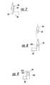
- FIG. 7is a partial view of another embodiment of a contact member according to the present invention.
- FIG. 8is a partial view of yet another embodiment of a contact member of according to the present invention.
- FIG. 9is a partial of view of yet another embodiment of a contact member according to the present invention.
- FIG. 10is a side view of a wafer support according to another embodiment of the present invention.
- FIG. 11is a top view of the wafer support of FIG. 10 .
- FIG. 12is a partial cross-sectional view of an arm and contact member of the wafer support of FIG. 10 .
- FIG. 13is a partial cross-sectional view of an arm and contact member according to another embodiment of the present invention.
- FIG. 14is a detail side view of an arm and contact member of the wafer support of FIG. 10 .
- FIG. 15is a partial cross-sectional view of an arm and contact member according to another embodiment of the present invention.
- FIG. 16is a partial cross-sectional view of an arm and contact member according to another embodiment of the present invention.
- FIG. 17is a side view of a wafer support according to another embodiment of the present invention.
- FIG. 18is a top view of the wafer support of FIG. 17 .
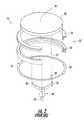
- a prior art epitaxial reactoris shown generally at 10 , including a susceptor assembly shown at 12 .
- Prior art reactor 10includes a reaction chamber 14 flanked on an upper side by an upper heat lamp array 16 and on a lower side by a lower heat lamp array 18 .
- Susceptor assembly 12is positioned within reaction chamber 14 , and is configured to support semiconductor wafer 20 within reaction chamber 14 .
- susceptor assembly 12includes several components, each of which must be heated by the upper and lower heat lamp arrays as the reaction chamber is heated to a process temperature.
- Susceptor assembly 12includes a susceptor 22 , typically of graphite construction, which acts to absorb heat energy from lamps 16 , 18 and to evenly distribute the heat energy to wafer 20 during epitaxial deposition.
- Susceptor 22typically includes a depression 36 on its top surface.
- wafer 20rests upon the susceptor, contacting the susceptor only at an outer edge 38 of the susceptor.
- susceptor 22rests directly upon posts 32 of tripod 30 .
- Tripod 30rests upon shaft 34 , which is configured to rotate under the influence of a prime mover (not shown).
- the reaction chamberis heated to a process temperature and a source gas containing semiconductor constituents is flowed from inlet 40 to outlet 42 , across a front side 46 of wafer 20 on its way through the reaction chamber.
- a source gas containing semiconductor constituentsis flowed from inlet 40 to outlet 42 , across a front side 46 of wafer 20 on its way through the reaction chamber.
- the semiconductor constituentsare adsorbed onto the wafer surface at high temperature and diffuse across the surface to form the epilayer.
- a susceptoris used to distribute heat to the wafer evenly. Epilayer growth is most uniform when an even temperature is maintained across the entire wafer.
- susceptor 22inhibits epilayer growth on the backside of the wafer by mechanically inhibiting gas flow to the back side of the wafer.
- Susceptor assembly 12also includes a structure called a Saturn ring 23 , including mating L-shaped rings 24 and 26 , each typically of graphite.
- Saturn ring 23is supported on posts 27 of Saturn ring support 28 , and is positioned around susceptor 22 such that the susceptor is free to rotate within the Saturn ring.
- Saturn ring 23is used to insulate and control heat transfer at an outer edge of the wafer. Reactors with susceptors typically experience cooling along the perimeter of the wafer due to heat loss to the gas flow.
- the Saturn ringabsorbs heat energy from the heat sources and helps prevent heat loss at the perimeter of the wafer, thereby keeping the temperature more uniform across the wafer and facilitating uniform epilayer growth.
- susceptor 22 , Saturn ring 23 , and Saturn ring support 28add thermal mass to the reaction chamber. For each wafer, these components must be heated and cooled multiple times during the epilayer growth process. In addition, these components periodically must be cleaned and/or replaced when deposits accumulate on the components from the epitaxial growth process. Therefore, use of these susceptor assembly components consumes great amounts of energy, time, and replacement materials.
- Reactor system 50includes an upper heat energy source 52 and a lower heat energy source 54 positioned on opposing sides of a reaction chamber 56 .
- upper heat energy source 52includes a plurality of heat lamps 62 positioned in an array extending across the top of reaction chamber 56
- lower heat energy source 54includes a plurality of heat lamps 64 positioned in an array rotated 90 degrees from heat lamps 62 and extending across the bottom of reaction chamber 56 .
- the upper and lower heat energy sourcesmay be RF coils, or another type of heat source.
- Wafer 58is heated by heat energy radiating from the upper heat source directly to a front side 66 of the wafer, and from the lower heat energy source directly to a back side 68 of the wafer.
- a wafer 58is positioned directly on a wafer support 60 within reaction chamber 56 during epilayer growth.
- Wafer support 60includes a hub 76 , which in turn includes a flared portion 78 configured to receive a tapered portion 80 of a shaft 82 .
- hub 76may incorporate another fastening mechanism to connect to shaft 82 , or may be formed integral with shaft 82 .
- shaft 82is connected at a lower end to a rotation and translation mechanism (not shown) that is configured to rotate, raise, and lower the shaft and wafer support within the reaction chamber. Rotation of the wafer ensures that radiant heat energy and source gases containing reactants are evenly distributed to all regions of the wafer.
- the shaft and wafer supportmay be configured only to rotate, or move up or down, or the shaft and wafer support may not move at all.
- Wafer support 60also includes arms 84 mounted at an inward end to hub 76 and extending radially outward from the hub, as shown in FIGS. 5 and 6.
- arms 84extend linearly outward at right angles from the hub.
- arms 84may extend outward in a curved, spiraling, angled, or other fashion.
- wafer support 60includes three arms. Alternatively, a different number of arms may be employed, such as one arm, or five arms. If one arm is used, that arm may support, for example, a curved member that extends sufficiently around a perimeter of the wafer to support the wafer.
- Arms 84usually are connected at a distal end to contact members 86 .
- contact members 86may be connected to arms 84 at some other location, such as intermediate the inward end and distal end of arms 84 .
- one contact member 86is positioned on each arm 84 .
- a plurality of contact membersmay be positioned on a single arm.
- wafer support 60includes voids 70 disposed adjacent arms 84 .
- voids 70typically extend from back side 68 of wafer 58 to a bottom 71 of the reaction chamber.
- Voids 70are configured to facilitate gas flow to back side 68 of wafer 58 .
- voids 70are configured to allow heat energy to radiate from lower heat energy source 54 , through the bottom 71 of the reaction chamber, through the voids 70 , directly to the back side 68 of wafer 58 , without being absorbed by an interfering susceptor or wafer support structure.
- reaction chamber 56including bottom 71 , and wafer support 60 are made of quartz, and are substantially thermally transparent, allowing radiant heat energy to pass directly through their structures.
- Contact members 86each typically include a shaft 88 and a tip 90 adjacent an upper end of the shaft. Each tip 90 typically includes a taper terminating in a point 92 .
- the taper of contact members 86is usually linear, extending inward towards a central longitudinal axis of the shaft at a 30 degree angle from the vertical axis. Alternatively, the taper may be of another angle, such as 45 degrees, or may be curved or some other irregular shape. For example, the tip may be hemispherical or elliptical.
- Point 92is typically fire polished and formed with a radius of 0.5 millimeters or less.
- Tip 90 and shaft 88may be formed as an integral structure, as shown in FIG. 5 .
- the contact member and armmay be separable.
- contact member 86may include a recess or hole 94 configured to mount upon a projection or post 96 of arm 84 .
- contact member 86may include a projection or post 98 configured to mount in a recess or hole 100 of arm 84 .
- contact member 86may include a shaft 102 that is taller than hole 100 , and which terminates in a tip 104 .
- the contact memberis removable from the arm and replaceable, such as may be required when deposits from the epi process build up on the surface of the contact member.
- the contact memberis often made of quartz, such that deposits do not easily build up on the contact member and radiant heat energy may easily pass through the contact member.
- a portion or the entirety of the contact membermay be formed of some other material, such as carbide.
- Contact members 86typically are configured with each tip 90 terminating in a point 92 such that minimum contact with wafer 58 is made during epilayer growth. Because the epilayer growth process is extremely sensitive to changes in wafer temperature, it is desirable to minimize contact with the wafer. Contact with the wafer will result in conductive heat transfer between the wafer and contact member. Conduction will result in a temperature gradient in the wafer that produces imperfect or uneven epilayer growth. In addition, the contact member may interfere in radiation of heat energy from the lower heat energy source to the wafer, thereby causing a region of the wafer to receive less heat energy, and be cooler, than surrounding regions. This interference will result in changes in epilayer growth in the cooler portion, thereby producing a heat shadow in the resultant epilayer. Such a heat shadow may interfere with later circuit fabrication in the epilayer, and is undesirable.
- one or more contact membersmay not terminate in a point, but may take some other shape, such as a ring or curved section.
- the wafer supportmay include a single ring-shaped contact member supporting the wafer near its outer edge, a single arm extending from the central hub to support the ring-shaped contact member, and a void adjacent the single arm extending to the bottom of the reaction chamber.
- Reaction chamber 56further includes an inlet 106 and an outlet 108 .
- the inletis configured to receive a gas mixture from a gas source (not shown) and direct the flow of the gas mixture around wafer 58 to outlet 108 .
- Outlet 108is configured to transport the gas mixture to an exhaust system (not shown).
- the gas mixtureincludes a source gas containing epilayer semiconductor constituents, such as silicon, gallium, arsenic, and germanium.
- the gas mixturemay also include a dopant gas including a dopant constituent, such as boron, phosphorous, arsenic, or antimony. These semiconductor and dopant constituents are transported to the wafer surface as volatile species suspended in the gas mixture. Typically, the constituents are adsorbed onto the substrate at high temperature and diffuse across the surface to form the epilayer.
- the gas mixturemay also include an etch gas, such as hydrogen chloride. It is also common for the gas mixture to include a carrier gas, such as hydrogen, which does not react with the wafer, but acts as a diluent within the gas mixture.
- Inlet 106 and outlet 108are horizontally disposed on opposite sides of reaction chamber 56 , and wafer support 60 is configured to hold wafer 58 intermediate the inlet and the outlet, such that the gas mixture flows from the inlet, around the wafer, and to the outlet.
- the gas mixtureflows to each of the front side 66 and the back side 68 of the wafer.
- the wafermay be raised or lowered within the reaction chamber to adjust gas flow around the wafer; for example, the wafer may be raised to increase gas flow to the back side of the wafer.
- the gas mixtureflows through the voids 70 in wafer support 60 .
- Wafer support 200includes a hub 202 that is flared and configured to mount to shaft 82 of the above described reactor system 50 .
- Shaft 82supports and rotates the wafer support within the reaction chamber 56 , described above.
- a hole 204is provided in the top of hub 202 , through which a thermocouple such as thermocouple 72 , described below, may be placed.
- Wafer support 202further includes three arms 206 extending radially outward from the hub. Alternatively, a smaller or greater number of arms may be provided. Arms 206 are typically circular in cross section, as shown in FIG. 12 . The top of the hub is typically formed horizontally flush with the top of the arms. Typically, the arms extend outward at right angles from the hub. However, it will be appreciated that the arms may extend at another predetermined angle, and/or may curve or spiral outward. Wafer support 200 includes voids 226 positioned adjacent arms 206 . Voids 226 are similar to voids 70 described above.
- Wafer support 200further includes a wafer contact assembly 208 coupled to each arm 206 adjacent a distal end of the arm.
- Each wafer contact assembly 208includes a contact member 210 mounted to an upwardly extending support member 212 , also referred to as post 212 , which is in turn mounted to a respective arm 206 by a coupling member 214 .
- contact member 210is formed of a shape with minimal surface area near the contact point with wafer 58 .
- contact member 210is triangular in shape, as shown in FIG. 12 .
- contact member 210may be cylindrical in shape, as shown at 210 a in FIG. 15, or may be of some other suitable shape.
- the contact memberis between about 0.02 and 0.20 inches in width, and preferably is about 0.06 inches in width, at its widest point.
- contact member 210typically extends inwardly and downwardly from post 212 .
- the contact memberextends downward from a point above the bottom surface 68 of wafer 58 to a point below the bottom surface 68 of the wafer.
- Contact member 210includes a downwardly sloping top surface portion 211 that is configured to contact an outer edge 59 of wafer 58 .
- Outer edge 59 of wafer 58typically includes top and bottom beveled portions 59 a and 59 c, and vertical portion 59 b.
- the bevelsare cut at an angle relative to the horizontal.
- the top surface portion 211 of contact member 210is angled downward at an angle relative to the horizontal, such that angle is greater than zero degrees and less than angle.
- contact member 210contacts the wafer 58 at one point of contact, thereby reducing the thermal interference caused by the wafer support on epilayer growth on the wafer.
- angleis about 22 degrees, and angle is between about zero and 22 degrees. In one preferred embodiment of the invention, angle is between zero and 15 degrees. In another preferred embodiment of the invention, angle is between about zero and 10 degrees, and in a particularly preferred embodiment, angle is about 4 degrees. It has been found that in these ranges, the wafer tends to center itself upon the three contact members when dropped by a paddle or other loading device onto the contact members 210 of wafer support 200 . The wafer vibrates slightly as it hits the contact members, and tends towards a centered position because of the inward slope of the contact members. Thus, successive wafers may be positioned in substantially the same position during the epilayer growth process, thereby assuring a uniform quality in the epilayers grown on the wafers.
- Post 212typically is mounted to coupling member 214 at a lower end and extends from a point below the bottom surface 68 of wafer 58 to a point above bottom surface 68 of the wafer.
- Post 212typically includes a rounded top 216 , which reduces interference in the gas flow to the outer edge 59 of wafer 58 .
- post 212is usually circular in cross section. Post 212 is typically positioned outward of the outer edge of the wafer.
- Coupling member 214includes a semi-cylindrical member 218 that extends slightly more than 180 degrees around arm 206 .
- the contact assemblyis typically quartz, and limited inherent flexibility in this material enables the walls of the semi-cylindrical member 218 to be temporarily bent slightly outward to enable installation of semi-cylindrical member 218 onto arm 206 .
- contact assembly 208may include a coupling member 214 b with a semi-cylindrical member that extends 180 degrees, or less, around arm 206 , as shown in FIG. 16 .
- Coupling member 214also typically includes a protrusion 220 extending from the semi-cylindrical member 218 into a slot 222 in the arm 206 .
- the mating of protrusion 220 and slot 222serve to secure coupling member 214 on arm 206 .
- the contact assemblymay include a coupling member 214 a without any protrusion, as shown in FIG. 13 .
- coupling member 214also may be secured to arm 206 by interference fit, welding or fusing, or other suitable attachment method.
- a heat absorbing ring 224may also be placed around an outside edge of the wafer 58 , adjacent an outer side of each of the wafer contact assemblies 208 .
- the heat absorbing ringis typically at least as thick as the wafer 58 .
- the heat absorbing ringis made of graphite. Alternatively, another suitable material may be used.
- the heat absorbing ringserves to absorb and evenly distribute heat to the edge of wafer 58 .
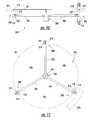
- FIGS. 17 and 18show another embodiment of a wafer support according to the present invention, indicated generally at 250 .
- Wafer support 250includes a hub 252 that is flared to receive shaft 82 , such that the wafer support may be supported and rotated within reaction chamber 56 , described above.
- Wafer support 250further includes radially extending arms 256 . Arms 256 typically extend at right angles from hub 252 . Alternatively, arms 256 may extend from the hub at another predetermined angle, and may be spiraled or curved.
- Wafer support 250includes voids 270 positioned adjacent arms 256 . Voids 270 are similar to voids 70 described above.
- a hole 254is positioned in the top of hub 252 , through which a thermocouple such as thermocouple 72 , described below, may be positioned.
- Each of arms 256typically includes an outer mount hole 258 positioned adjacent a distal end of the arm.
- Each of the armsalso may include an inner mount hole 260 positioned intermediate the distal and proximate ends of the arm.
- Each of mount holes 258 , 260is adapted to receive a respective contact member 262 .
- the contact membersare installed in outer mount holes 258 adjacent a distal end of each arm.
- contact membersmay be installed in inner mount holes 260 , in positions shown in dashed lines at 262 a intermediate the proximate and distal ends of each arm.
- contact members 262may be installed in both holes 258 and 260 , or in a combination of holes selected from among holes 258 and 260 .
- the contact membersmay be formed integrally with the arms, or may attach to the arms in another suitable manner, and the arms may not include mount holes.
- Each contact member 262includes a shaft 264 terminating in a tip 266 .
- Tip 266is typically a 45 degree cone.
- tip 266may be a cone of another predetermined angle, or may be rounded or polygonal.
- shaft 264is between about 0.02 and 0.20 inches in diameter, and is preferably about 0.06 inches in diameter.
- shaft 264may have a larger or smaller diameter.
- contact member 262is between about 0.5 and 2 inches in height.
- the shaftis between about 0.8 and 1.4 inches in height, and in one particularly preferable embodiment of the invention is about 1.2 inches in height.
- the contact membermay be longer or shorter.
- a heat absorbing ring 268may also be placed around an outside edge of the wafer 58 , adjacent an outer side of each of the contact members 262 .
- the heat absorbing ringtypically is at least as thick as the wafer 58 , and is made of graphite. Alternatively, another suitable material may be used.
- the heat absorbing ringserves to absorb and evenly distribute heat to the edge of wafer 58 .
- FIGS. 10-18have the advantage of being configured to support the wafer adjacent an outer edge of the wafer. This reduces imperfections to the underside of wafer caused by supporting the wafer by direct contact with the underside. When used in combination with a heat absorbing ring to stabilize heat transfer to the outer edge of the ring, fewer epilayer imperfections result.
- these embodimentsutilize round arms, and a reduced-height hub, each of which minimizes material near the wafer, thereby reducing thermal interference in the epilayer growth process and improving gas flow to the underside of the wafer.
- a methodmay be practiced for susceptorless epitaxial growth of a layer of semiconductor material on a semiconductor wafer.
- the methodincludes placing wafer 58 within reaction chamber 56 and supporting the wafer directly on a contact member 86 of wafer support 60 .
- the present methodwill be described with reference to wafer support 60 , however it will be appreciated that wafer supports 200 , 250 also may be used in connection with the method.
- the methodfurther includes heating the wafer to a predetermined temperature without also heating a susceptor. Typically, the heat energy is radiated directly to a front and back side of the wafer.
- the radiant energypasses through voids 70 in wafer support 60 , shown in FIG. 6, directly to the back side of the wafer.
- the voids in wafer support 60enable the heat energy source to heat the wafer without substantial structural interference by a susceptor or the wafer support.
- the voidsdecrease the thermal mass of the wafer support. Therefore, compared to prior reactors with susceptors, the present invention enables the wafer to be heated more directly and quickly.
- Reaction chamber 56is heated by heat energy sources 52 , 54 until wafer 58 reaches a predetermined process temperature at which it is desired that epilayer growth occur.
- the process temperaturetypically is between 900 and 1200 degrees Celsius.
- the methodmay also include positioning a thermocouple 72 proximate wafer 58 to sense the temperature of the reaction chamber adjacent the wafer. To reduce thermal interference with the wafer, the thermocouple typically does not contact the wafer. As shown in FIG. 4, thermocouple 72 may be covered by a cap 74 , typically of graphite material.
- Cap 74absorbs heat energy and insulates thermocouple 72 such that the thermocouple is not subject to temporary temperature fluctuations caused, for example, by convection due to gas currents in the reaction chamber, and may measure more accurately the temperature adjacent the wafer.
- the thermocoupleis used to control the amount of heat added to the reaction chamber, such that the temperature in the reaction chamber may be precisely controlled.
- the methodalso includes flowing a source gas including semiconductor constituents across the wafer to facilitate epilayer growth on a surface of the wafer.
- Source gasis flowed through void 70 to reach the back side of the wafer.
- the methodmay also include flowing a dopant gas, etch gas, and/or carrier gas to a front and back side of the wafer, the gases reaching the back side through void 70 .
- the gasesare simultaneously flowed to the front and back side of the wafer.
- the gasesmay be flowed alternately to a front side and a back side of the wafer, or flowed only to one of the front or back sides of the wafer. Over time, deposits from the epilayer growth process build up on the components within reaction chamber 56 .
- Such depositsmay contaminate a growing epilayer, and must be removed periodically.
- the present inventionmay include removing the contact member from the wafer support and replacing the contact member. Typically, this is accomplished using a contact member as shown in FIGS. 7-9.
- the depositsmay also be removed by flowing an etch gas through the reaction chamber.
- the methodmay include rotating the wafer within the reaction chamber during growth of the epitaxial layer.
- the methodmay also include moving the wafer up and down within the reaction chamber during growth of the epitaxial layer to adjust the heat and/or gas mixture reaching a region of the wafer.
- the methodmay also include deposition of a gettering layer on the back side of the wafer during the epilayer deposition cycle.
- Getteringis a natural process by which defects in the crystal lattice attract impurities within the semiconductor material. The impurities are attracted to the defects due to the strain the defects create in the crystal lattice. As a result, impurities tend to precipitate around the defects.
- the methodmay include intentionally creating defects, or gettering sites, in the crystal lattice to attract contaminants away from the epilayer. For example, the method may include depositing a polysilicon layer on the back surface of the wafer to create strain within the crystal lattice.
- the methodmay also include loading a wafer into the reaction chamber by an understructure, such as spatula 110 , 110 a, or 110 b, shown in FIG. 6 .
- an understructuresuch as spatula 110 , 110 a, or 110 b, shown in FIG. 6 .
- the waferis brought into the reaction chamber on the spatula, to a position indicated at 58 a in FIG. 3 .
- Wafer support 60may then be moved up to raise the wafer off of spatula 110 , at which time spatula 110 is withdrawn from the reaction chamber.
- Wafer support 60then typically is lowered into position for epilayer growth.
- Mechanical loading of the wafer by such an understructureis less complex and significantly decreases loading time compared with vacuum loading mechanisms employed by reactors with susceptors.
- the methodalso may include centering the wafer on the wafer support by use of inwardly extending and downwardly sloping portions of contact members 210 , as described above.
- epitaxial growthmay occur in a reactor system without the susceptor 22 , Saturn ring 23 , or Saturn ring support 28 found on prior reactors. Therefore, the reaction chamber may be heated and cooled more quickly, with less energy, and epilayer growth may be achieved in a shorter cycle time per wafer, resulting in a finished epitaxial wafer of reduced cost.
- semiconductor deposition on reactor components and contamination therefromis significantly reduced. It is believed that lower quantities of source gases are required by the present invention, because incidental deposition on other reactor components is reduced.
- the present inventionmay be used to prevent autodoping during the epilayer growth process, because an epilayer may be deposited on the back side of the wafer.
- direct, even heating of the wafer on both sides through the voids in the wafer supportreduces thermal strain in the wafer experienced by reactors where heat transfer occurs between the wafer and a susceptor.
- This inventionis applicable to the semiconductor processing industry, and particularly to epitaxial reactor systems for use in growing an epitaxial layer of semiconductor material on a semiconductor wafer.
Landscapes
- Chemical & Material Sciences (AREA)
- Engineering & Computer Science (AREA)
- Organic Chemistry (AREA)
- Metallurgy (AREA)
- Materials Engineering (AREA)
- Chemical Kinetics & Catalysis (AREA)
- General Physics & Mathematics (AREA)
- Power Engineering (AREA)
- Condensed Matter Physics & Semiconductors (AREA)
- Microelectronics & Electronic Packaging (AREA)
- Computer Hardware Design (AREA)
- General Chemical & Material Sciences (AREA)
- Physics & Mathematics (AREA)
- Manufacturing & Machinery (AREA)
- Mechanical Engineering (AREA)
- Crystallography & Structural Chemistry (AREA)
- Toxicology (AREA)
- Health & Medical Sciences (AREA)
- Chemical Vapour Deposition (AREA)
Abstract
Description
This application is a continuation-in-part of application Ser. No. 09/353,796 filed Jul. 14, 1999 and application Ser. No. 09/353,197 filed Jul. 14, 1999, the disclosures of which are herein incorporated by reference.
The present invention relates generally to semiconductor wafer fabrication, and more specifically to a reactor system and wafer support for use during epitaxial growth of a semiconductor material on a semiconductor wafer.
In the semiconductor wafer manufacturing industry, thin epitaxial layers of semiconductor material, such as silicon or gallium arsenide, are grown on a surface of a semiconductor wafer. These epitaxial layers, commonly referred to as epilayers, form the material within which many modern integrated circuits are fabricated. In addition, many other devices, including optoelectric sensors, light emitting diodes, and micromachined mechanical devices, may be fabricated from epilayer material. As epilayers are a fundamental building block for many technologies, is critical that they be manufactured as efficiently and defect-free as possible, to reduce the cost and increase the quality of the epilayer.
Epilayers may be grown according to a variety of methods, including molecular beam epitaxy (MBE), vapor phase epitaxy (VPE), and liquid phase epitaxy (LPE). In a vapor phase epitaxial reactor, epilayer semiconductor constituents, such as silicon, gallium, arsenic, and germanium, and various dopants such as boron, phosphorous, arsenic, and antimony, are transported to the substrate surface as volatile species suspended in a vapor. Typically, the species are adsorbed onto the substrate at high temperature and diffuse across the surface to form the epilayer.
The VPE process takes place in a reactor including a heat energy source, such as radio frequency (RF) coils or heat lamps, and a susceptor. The susceptor typically is a solid graphite disk underlying and extending to the edge of the wafer and is substantially thicker than the wafer. One or more wafers are placed into the reactor directly on the susceptor, and the heat energy source is activated to heat the susceptor and the wafer. Where a RF heat energy source is used, the susceptor absorbs RF heat energy and conducts heat energy to the wafer. Where heat lamps are used, the susceptor absorbs heat energy and evenly distributes heat within the wafer, making the wafer less susceptible to temperature gradients within the reaction chamber.
After the wafer has been heated, gas containing the semiconductor constituents for epitaxial growth is introduced to the reactor through an inlet and flowed toward the wafer. Constituents are deposited on the front side of the wafer to form the epilayer. However, contact between the susceptor and the wafer inhibits gas flow to the back side of the wafer, such that constituents do not reach the back side and epilayer growth does not occur on the back side.
Several problems exist with reactors having susceptors. First, the thermal mass of the susceptor must be heated within the reactor along with the wafer before the epitaxial growth process may begin. For each wafer, it is common for the reaction chamber to be heated and cooled several times during the epitaxial growth cycle. For example, after a silicon wafer is inserted into the reaction chamber, the temperature is typically raised for a hydrogen bake of the wafer, which removes silicon dioxide contaminants from the wafer. The chamber is then cooled for epilayer deposition, and is again cooled before unloading of the wafer. After deposition, the chamber typically is heated again, and etch gases, such as hydrogen chloride, are flowed through the chamber to remove semiconductor material from the chamber and susceptor.
When producing epitaxial wafers on a mass scale, heating up and cooling down the susceptor consumes significant amounts of time and energy. In addition, the susceptors require frequent cleaning as semiconductor materials build up on the surface of the susceptors during the epitaxial growth process. Without cleaning, deposits may flake off and contaminate the epilayer growth process. In addition, susceptors must be replaced as their surfaces degrade from repeated epilayer deposition and cleaning, further increasing the materials costs associated with wafer manufacture.
Use of a susceptor for epilayer growth also may induce thermal stresses within the wafer. For example, where RF coils are used to heat the susceptor, the back side of the wafer adjacent the susceptor typically will be hotter than the front side of the wafer during epilayer growth, causing the wafer to bow. Thermally induced strain will develop in the lattice of the bowed wafer as the wafer cools.
Compared to other fabrication procedures, epilayer growth takes place under closely controlled conditions. A prior step in the wafer manufacture process may leave contaminants or imperfections on the surface of the wafer. One effect of the epilayer growth process is to remove these contaminants and correct these imperfections. However, reactors that grow an epilayer on only one side of a wafer, such as reactors that use susceptors, do not remove contaminants or perfect the imperfections on the back side of the wafer. These imperfections and contaminants on the back side may adversely affect a downstream circuit fabrication, test, or measurement procedure.
Where only the front side of a wafer is being coated with an epilayer, there is a risk that dopants within the substrate of the wafer will escape from the back side of the substrate at high temperatures during the epitaxial growth process, enter the gas flow, and contaminate the epilayer growth process on the front side of the wafer. This contamination process is referred to as autodoping, and is highly undesirable.
In addition, use of a susceptor in a reactor requires that the wafer be loaded onto the susceptor by a paddle that picks the wafer up by its top side. Some current reactors commonly utilize paddles that lift the wafer by creating a vacuum through direct suction or according to the Bernoulli effect. Loading and unloading through such vacuum operative paddles is slow, and consumes valuable cycle time per wafer.
A reactor system with an associated wafer support device is provided for use in the growth of an epitaxial layer of semiconductor material on a semiconductor wafer. The reactor system includes a reaction chamber including an inlet and an outlet configured to flow a source gas through the reaction chamber. The reaction system also includes a wafer support mounted at least partially within the reaction chamber, and a semiconductor wafer supported adjacent an outer edge by the wafer support. The wafer support device typically includes a hub and an arm extending outwardly from the hub. The wafer support device also typically includes a contact member coupled to the arm. In some embodiments a portion of the contact member extending downward relative to the back side of the wafer. The downwardly extending portion is configured to contact and support the wafer during epitaxial growth of semiconductor material onto the wafer. The contact member may be triangular or circular in cross section, and may be coupled to the arm via an upwardly extending support member and coupling member. In addition, the wafer support may include a hub and at least three arms extending radially outward from the hub. The wafer support may also include at least three contact members, each contact member being coupled to a respective arm. Each contact member includes a respective tip configured to directly contact the back side of the wafer adjacent an outer edge of the wafer and to support the wafer in a substantially horizontal orientation within the reactor system. The wafer support does not include a susceptor.
FIG. 1 is a cross-sectional view of a prior art epitaxial reactor including a susceptor.
FIG. 2 is a partial cutaway exploded perspective view of a susceptor assembly of the prior art epitaxial reactor of FIG.1.
FIG. 3 is a cross-sectional view of a reactor system according to the present invention.
FIG. 4 is a cross-sectional view of another embodiment of a reactor system according to the present invention.
FIG. 5 is a front view of a wafer support according to the present invention.
FIG. 6 is a top view of the wafer support of FIG.5.
FIG. 7 is a partial view of another embodiment of a contact member according to the present invention.
FIG. 8 is a partial view of yet another embodiment of a contact member of according to the present invention.
FIG. 9 is a partial of view of yet another embodiment of a contact member according to the present invention.
FIG. 10 is a side view of a wafer support according to another embodiment of the present invention.
FIG. 11 is a top view of the wafer support of FIG.10.
FIG. 12 is a partial cross-sectional view of an arm and contact member of the wafer support of FIG.10.
FIG. 13 is a partial cross-sectional view of an arm and contact member according to another embodiment of the present invention.
FIG. 14 is a detail side view of an arm and contact member of the wafer support of FIG.10.
FIG. 15 is a partial cross-sectional view of an arm and contact member according to another embodiment of the present invention.
FIG. 16 is a partial cross-sectional view of an arm and contact member according to another embodiment of the present invention.
FIG. 17 is a side view of a wafer support according to another embodiment of the present invention.
FIG. 18 is a top view of the wafer support of FIG.17.
Referring initially to FIG. 1, a prior art epitaxial reactor is shown generally at10, including a susceptor assembly shown at12.Prior art reactor 10 includes areaction chamber 14 flanked on an upper side by an upperheat lamp array 16 and on a lower side by a lowerheat lamp array 18.Susceptor assembly 12 is positioned withinreaction chamber 14, and is configured to supportsemiconductor wafer 20 withinreaction chamber 14.
As shown in FIGS. 1 and 2,susceptor assembly 12 includes several components, each of which must be heated by the upper and lower heat lamp arrays as the reaction chamber is heated to a process temperature.Susceptor assembly 12 includes asusceptor 22, typically of graphite construction, which acts to absorb heat energy fromlamps wafer 20 during epitaxial deposition.Susceptor 22 typically includes adepression 36 on its top surface. During epilayer growth,wafer 20 rests upon the susceptor, contacting the susceptor only at anouter edge 38 of the susceptor. As shown in FIG. 1,susceptor 22 rests directly uponposts 32 oftripod 30.Tripod 30 rests uponshaft 34, which is configured to rotate under the influence of a prime mover (not shown).
In operation, the reaction chamber is heated to a process temperature and a source gas containing semiconductor constituents is flowed frominlet 40 tooutlet 42, across afront side 46 ofwafer 20 on its way through the reaction chamber. Typically, the semiconductor constituents are adsorbed onto the wafer surface at high temperature and diffuse across the surface to form the epilayer.
In prior art reactors such as10, a susceptor is used to distribute heat to the wafer evenly. Epilayer growth is most uniform when an even temperature is maintained across the entire wafer. In addition,susceptor 22 inhibits epilayer growth on the backside of the wafer by mechanically inhibiting gas flow to the back side of the wafer.
However,susceptor 22,Saturn ring 23, andSaturn ring support 28 add thermal mass to the reaction chamber. For each wafer, these components must be heated and cooled multiple times during the epilayer growth process. In addition, these components periodically must be cleaned and/or replaced when deposits accumulate on the components from the epitaxial growth process. Therefore, use of these susceptor assembly components consumes great amounts of energy, time, and replacement materials.
Turning now to FIG. 3, an epitaxial reactor system according to the present invention is shown generally at50.Reactor system 50 includes an upperheat energy source 52 and a lowerheat energy source 54 positioned on opposing sides of areaction chamber 56. Typically, upperheat energy source 52 includes a plurality ofheat lamps 62 positioned in an array extending across the top ofreaction chamber 56, and lowerheat energy source 54 includes a plurality ofheat lamps 64 positioned in an array rotated 90 degrees fromheat lamps 62 and extending across the bottom ofreaction chamber 56. Alternatively, the upper and lower heat energy sources may be RF coils, or another type of heat source.Wafer 58 is heated by heat energy radiating from the upper heat source directly to afront side 66 of the wafer, and from the lower heat energy source directly to aback side 68 of the wafer.
Awafer 58 is positioned directly on awafer support 60 withinreaction chamber 56 during epilayer growth.Wafer support 60 includes ahub 76, which in turn includes a flaredportion 78 configured to receive a taperedportion 80 of ashaft 82. Alternatively,hub 76 may incorporate another fastening mechanism to connect toshaft 82, or may be formed integral withshaft 82. Typically,shaft 82 is connected at a lower end to a rotation and translation mechanism (not shown) that is configured to rotate, raise, and lower the shaft and wafer support within the reaction chamber. Rotation of the wafer ensures that radiant heat energy and source gases containing reactants are evenly distributed to all regions of the wafer. Alternatively, the shaft and wafer support may be configured only to rotate, or move up or down, or the shaft and wafer support may not move at all.
As shown in FIG. 6,wafer support 60 includesvoids 70 disposedadjacent arms 84. Wherewafer 58 is positioned for epilayer growth onwafer support 60 withinreaction chamber 56, voids70 typically extend from backside 68 ofwafer 58 to a bottom71 of the reaction chamber.Voids 70 are configured to facilitate gas flow to backside 68 ofwafer 58. In addition, voids70 are configured to allow heat energy to radiate from lowerheat energy source 54, through the bottom71 of the reaction chamber, through thevoids 70, directly to theback side 68 ofwafer 58, without being absorbed by an interfering susceptor or wafer support structure. Typically,reaction chamber 56, including bottom71, andwafer support 60 are made of quartz, and are substantially thermally transparent, allowing radiant heat energy to pass directly through their structures.
In the embodiments shown in FIGS. 7-9, the contact member is removable from the arm and replaceable, such as may be required when deposits from the epi process build up on the surface of the contact member. The contact member is often made of quartz, such that deposits do not easily build up on the contact member and radiant heat energy may easily pass through the contact member. Alternatively a portion or the entirety of the contact member may be formed of some other material, such as carbide.
Alternatively, one or more contact members may not terminate in a point, but may take some other shape, such as a ring or curved section. For example, the wafer support may include a single ring-shaped contact member supporting the wafer near its outer edge, a single arm extending from the central hub to support the ring-shaped contact member, and a void adjacent the single arm extending to the bottom of the reaction chamber.
Where it is desired to etch material from thewafer 58,wafer support 60, orreaction chamber 56, the gas mixture may also include an etch gas, such as hydrogen chloride. It is also common for the gas mixture to include a carrier gas, such as hydrogen, which does not react with the wafer, but acts as a diluent within the gas mixture.
In FIGS. 10 and 11, a wafer support according to an another embodiment of the present invention is shown generally at200.Wafer support 200 includes ahub 202 that is flared and configured to mount toshaft 82 of the above describedreactor system 50.Shaft 82 supports and rotates the wafer support within thereaction chamber 56, described above. Ahole 204 is provided in the top ofhub 202, through which a thermocouple such asthermocouple 72, described below, may be placed.
It is desirable to reduce the thermal mass of the contact member near the wafer, in order to reduce thermal interference that may cause abnormalities in the epilayer growth on the wafer, as described above. Thus,contact member 210 is formed of a shape with minimal surface area near the contact point withwafer 58. Typically,contact member 210 is triangular in shape, as shown in FIG.12. Alternatively,contact member 210 may be cylindrical in shape, as shown at210ain FIG. 15, or may be of some other suitable shape. Typically, the contact member is between about 0.02 and 0.20 inches in width, and preferably is about 0.06 inches in width, at its widest point.
As shown in FIG. 14,contact member 210 typically extends inwardly and downwardly frompost 212. The contact member extends downward from a point above thebottom surface 68 ofwafer 58 to a point below thebottom surface 68 of the wafer.Contact member 210 includes a downwardly slopingtop surface portion 211 that is configured to contact anouter edge 59 ofwafer 58.Outer edge 59 ofwafer 58 typically includes top and bottombeveled portions vertical portion 59b.The bevels are cut at an angle relative to the horizontal. Thetop surface portion 211 ofcontact member 210 is angled downward at an angle relative to the horizontal, such that angle is greater than zero degrees and less than angle. Thus,contact member 210 contacts thewafer 58 at one point of contact, thereby reducing the thermal interference caused by the wafer support on epilayer growth on the wafer.
Typically, angle is about 22 degrees, and angle is between about zero and 22 degrees. In one preferred embodiment of the invention, angle is between zero and 15 degrees. In another preferred embodiment of the invention, angle is between about zero and 10 degrees, and in a particularly preferred embodiment, angle is about 4 degrees. It has been found that in these ranges, the wafer tends to center itself upon the three contact members when dropped by a paddle or other loading device onto thecontact members 210 ofwafer support 200. The wafer vibrates slightly as it hits the contact members, and tends towards a centered position because of the inward slope of the contact members. Thus, successive wafers may be positioned in substantially the same position during the epilayer growth process, thereby assuring a uniform quality in the epilayers grown on the wafers.
Couplingmember 214 includes asemi-cylindrical member 218 that extends slightly more than 180 degrees aroundarm 206. The contact assembly is typically quartz, and limited inherent flexibility in this material enables the walls of thesemi-cylindrical member 218 to be temporarily bent slightly outward to enable installation ofsemi-cylindrical member 218 ontoarm 206. Alternatively,contact assembly 208 may include acoupling member 214bwith a semi-cylindrical member that extends 180 degrees, or less, aroundarm 206, as shown in FIG.16.
Couplingmember 214 also typically includes aprotrusion 220 extending from thesemi-cylindrical member 218 into aslot 222 in thearm 206. The mating ofprotrusion 220 and slot222 serve to securecoupling member 214 onarm 206. Alternatively, the contact assembly may include acoupling member 214awithout any protrusion, as shown in FIG.13. It will be understood thatcoupling member 214 also may be secured toarm 206 by interference fit, welding or fusing, or other suitable attachment method.
Aheat absorbing ring 224 may also be placed around an outside edge of thewafer 58, adjacent an outer side of each of thewafer contact assemblies 208. The heat absorbing ring is typically at least as thick as thewafer 58. Typically the heat absorbing ring is made of graphite. Alternatively, another suitable material may be used. The heat absorbing ring serves to absorb and evenly distribute heat to the edge ofwafer 58.
FIGS. 17 and 18 show another embodiment of a wafer support according to the present invention, indicated generally at250.Wafer support 250 includes ahub 252 that is flared to receiveshaft 82, such that the wafer support may be supported and rotated withinreaction chamber 56, described above.Wafer support 250 further includes radially extendingarms 256.Arms 256 typically extend at right angles fromhub 252. Alternatively,arms 256 may extend from the hub at another predetermined angle, and may be spiraled or curved.Wafer support 250 includesvoids 270 positionedadjacent arms 256.Voids 270 are similar tovoids 70 described above. Ahole 254 is positioned in the top ofhub 252, through which a thermocouple such asthermocouple 72, described below, may be positioned.
Each ofarms 256 typically includes anouter mount hole 258 positioned adjacent a distal end of the arm. Each of the arms also may include aninner mount hole 260 positioned intermediate the distal and proximate ends of the arm. Each of mount holes258,260 is adapted to receive arespective contact member 262. Preferably, the contact members are installed in outer mount holes258 adjacent a distal end of each arm. Alternatively, contact members may be installed in inner mount holes260, in positions shown in dashed lines at262aintermediate the proximate and distal ends of each arm. In addition,contact members 262 may be installed in bothholes holes
Eachcontact member 262 includes ashaft 264 terminating in atip 266.Tip 266 is typically a 45 degree cone. Alternatively tip266 may be a cone of another predetermined angle, or may be rounded or polygonal. In an exemplary embodiment of the invention,shaft 264 is between about 0.02 and 0.20 inches in diameter, and is preferably about 0.06 inches in diameter. Alternatively,shaft 264 may have a larger or smaller diameter. Typically,contact member 262 is between about 0.5 and 2 inches in height. In one preferable embodiment of the invention, the shaft is between about 0.8 and 1.4 inches in height, and in one particularly preferable embodiment of the invention is about 1.2 inches in height. Alternatively, the contact member may be longer or shorter.
Aheat absorbing ring 268 may also be placed around an outside edge of thewafer 58, adjacent an outer side of each of thecontact members 262. The heat absorbing ring typically is at least as thick as thewafer 58, and is made of graphite. Alternatively, another suitable material may be used. The heat absorbing ring serves to absorb and evenly distribute heat to the edge ofwafer 58.
The embodiments of FIGS. 10-18 have the advantage of being configured to support the wafer adjacent an outer edge of the wafer. This reduces imperfections to the underside of wafer caused by supporting the wafer by direct contact with the underside. When used in combination with a heat absorbing ring to stabilize heat transfer to the outer edge of the ring, fewer epilayer imperfections result. In addition, these embodiments utilize round arms, and a reduced-height hub, each of which minimizes material near the wafer, thereby reducing thermal interference in the epilayer growth process and improving gas flow to the underside of the wafer.
According to the present invention, a method may be practiced for susceptorless epitaxial growth of a layer of semiconductor material on a semiconductor wafer. The method includes placingwafer 58 withinreaction chamber 56 and supporting the wafer directly on acontact member 86 ofwafer support 60. The present method will be described with reference towafer support 60, however it will be appreciated that wafer supports200,250 also may be used in connection with the method. The method further includes heating the wafer to a predetermined temperature without also heating a susceptor. Typically, the heat energy is radiated directly to a front and back side of the wafer.
The radiant energy passes throughvoids 70 inwafer support 60, shown in FIG. 6, directly to the back side of the wafer. The voids inwafer support 60 enable the heat energy source to heat the wafer without substantial structural interference by a susceptor or the wafer support. In addition, the voids decrease the thermal mass of the wafer support. Therefore, compared to prior reactors with susceptors, the present invention enables the wafer to be heated more directly and quickly.
The method also includes flowing a source gas including semiconductor constituents across the wafer to facilitate epilayer growth on a surface of the wafer. Source gas is flowed throughvoid 70 to reach the back side of the wafer. The method may also include flowing a dopant gas, etch gas, and/or carrier gas to a front and back side of the wafer, the gases reaching the back side throughvoid 70. Typically, the gases are simultaneously flowed to the front and back side of the wafer. Alternatively, the gases may be flowed alternately to a front side and a back side of the wafer, or flowed only to one of the front or back sides of the wafer. Over time, deposits from the epilayer growth process build up on the components withinreaction chamber 56. Such deposits may contaminate a growing epilayer, and must be removed periodically. The present invention may include removing the contact member from the wafer support and replacing the contact member. Typically, this is accomplished using a contact member as shown in FIGS. 7-9. The deposits may also be removed by flowing an etch gas through the reaction chamber.
To distribute heat energy and gases flowing throughreaction chamber 56 towafer 58 evenly, the method may include rotating the wafer within the reaction chamber during growth of the epitaxial layer. The method may also include moving the wafer up and down within the reaction chamber during growth of the epitaxial layer to adjust the heat and/or gas mixture reaching a region of the wafer.
The method may also include deposition of a gettering layer on the back side of the wafer during the epilayer deposition cycle. Gettering is a natural process by which defects in the crystal lattice attract impurities within the semiconductor material. The impurities are attracted to the defects due to the strain the defects create in the crystal lattice. As a result, impurities tend to precipitate around the defects. The method may include intentionally creating defects, or gettering sites, in the crystal lattice to attract contaminants away from the epilayer. For example, the method may include depositing a polysilicon layer on the back surface of the wafer to create strain within the crystal lattice.
The method may also include loading a wafer into the reaction chamber by an understructure, such asspatula Wafer support 60 may then be moved up to raise the wafer off ofspatula 110, at whichtime spatula 110 is withdrawn from the reaction chamber.Wafer support 60 then typically is lowered into position for epilayer growth. Mechanical loading of the wafer by such an understructure is less complex and significantly decreases loading time compared with vacuum loading mechanisms employed by reactors with susceptors. The method also may include centering the wafer on the wafer support by use of inwardly extending and downwardly sloping portions ofcontact members 210, as described above.
According to the present invention, epitaxial growth may occur in a reactor system without thesusceptor 22,Saturn ring 23, orSaturn ring support 28 found on prior reactors. Therefore, the reaction chamber may be heated and cooled more quickly, with less energy, and epilayer growth may be achieved in a shorter cycle time per wafer, resulting in a finished epitaxial wafer of reduced cost. In addition, semiconductor deposition on reactor components and contamination therefrom is significantly reduced. It is believed that lower quantities of source gases are required by the present invention, because incidental deposition on other reactor components is reduced. In addition, the present invention may be used to prevent autodoping during the epilayer growth process, because an epilayer may be deposited on the back side of the wafer. Finally, direct, even heating of the wafer on both sides through the voids in the wafer support reduces thermal strain in the wafer experienced by reactors where heat transfer occurs between the wafer and a susceptor.
This invention is applicable to the semiconductor processing industry, and particularly to epitaxial reactor systems for use in growing an epitaxial layer of semiconductor material on a semiconductor wafer.
It is believed that the disclosure set forth above encompasses multiple distinct inventions with independent utility. While each of these inventions has been disclosed in its preferred form, the specific embodiments thereof as disclosed and illustrated herein are not to be considered in a limiting sense as numerous variations are possible. The subject matter of the inventions includes all novel and non-obvious combinations and subcombinations of the various elements, features, functions and/or properties disclosed herein. No single feature, function, element or property of the disclosed embodiments is essential to all of the disclosed inventions. Similarly, where the claims recite “a” or “a first” element or the equivalent thereof, such claims should be understood to include incorporation of one or more such elements, neither requiring nor excluding two or more such elements.
It is believed that the following claims particularly point out certain combinations and subcombinations that are directed to one of the disclosed inventions and are novel and non-obvious. Inventions embodied in other combinations and subcombinations of features, functions, elements and/or properties may be claimed through amendment of the present claims or presentation of new claims in this or a related application. Such amended or new claims, whether they are directed to a different invention or directed to the same invention, whether different, broader, narrower or equal in scope to the original claims, are also regarded as included within the subject matter of the inventions of the present disclosure.
Claims (21)
1. A wafer support device to support a semiconductor wafer within a reactor system during epitaxial growth of a semiconductor material onto the wafer, the wafer including a back side, the wafer support device comprising:
a hub;
a plurality of arms extending outwardly from the hub; and
a plurality of spaced-apart contact members, each contact member being coupled to a respective one of the arms, and each contact member including a portion configured to contact the back side of the wafer and to support the wafer during epitaxial growth of semiconductor material onto the wafer;
wherein the portion of each contact member extends downward relative to the back side of the wafer.
2. The wafer support device ofclaim 1 , wherein the wafer includes an outer edge, and each of the contact members is configured to support the wafer adjacent the outer edge.
3. The wafer support device ofclaim 1 , wherein the downwardly extending portion of each contact member extends downward at an angle of greater than zero and less than about 22 degrees relative to the back side of the wafer.
4. The wafer support device ofclaim 1 , wherein the downwardly extending portion of each contact member extends downward at an angle of between zero and about 15 degrees relative to the back side of the wafer.
5. The wafer support device ofclaim 1 , wherein at least one of the contact members includes a triangular cross section.
6. The wafer support device ofclaim 1 , wherein at least one of the contact members includes a circular cross section.
7. The wafer support device ofclaim 1 , wherein the downwardly extending portion of each contact member extends inwardly from above the back side of the wafer to below the backside of the wafer.
8. The wafer support device ofclaim 1 , wherein the wafer includes an outer edge, and wherein each of the contact members is configured to contact and support the wafer adjacent the outer edge.
9. The wafer support device ofclaim 8 , further comprising:
a plurality of upwardly extending support members, each upwardly extending support member being coupled at a lower end to a distal end of a respective arm and at an upper end to a corresponding contact member.
10. The wafer support device ofclaim 9 , wherein each of the upwardly extending support members is positioned outside of the outer edge of the wafer.
11. The wafer support device ofclaim 9 , wherein each of the upwardly extending support members extends from below the back side of the wafer to above the back side of the wafer.
12. The wafer support device ofclaim 9 , further comprising:
a plurality of coupling members, each coupling member securing a respective upwardly extending support member to the distal end of a corresponding arm.
13. The wafer support device ofclaim 12 , wherein at least one of the coupling members includes a semi-cylindrical base.
14. The wafer support device ofclaim 12 , wherein at least one of the coupling members includes a protrusion, and the arm includes a hole adapted to receive the protrusion.
15. The wafer support device ofclaim 1 , wherein the arm includes a circular cross section.
16. The wafer support device ofclaim 1 , wherein the hub includes a top that is substantially horizontally flush with the arms.
17. The wafer support device ofclaim 1 , wherein the plurality of arms includes three arms extending radially outward from the hub, and the plurality of contact members includes three contact members, each of the contact members being coupled to a respective arm, wherein a portion of each of the contact members extends downward relative to the back side of the wafer, each of the downwardly extending portions being configured to contact and support the wafer during epitaxial growth of semiconductor material onto the wafer.
18. The wafer support device ofclaim 17 , wherein the downwardly extending portion of each contact member extends downward at an angle of between zero and about 22 degrees.
19. The wafer support device ofclaim 17 , wherein the downwardly extending portion of each contact member extends downward at an angle of between zero and about 15 degrees.
20. A reactor system for use in growth of an epitaxial layer of semiconductor material on a semiconductor wafer, the reactor system comprising:
a reaction chamber including an inlet and an outlet configured to flow a source gas through the reaction chamber;
a wafer support mounted at least partially within the reaction chamber, the wafer support including at least three contact members, each contact member including a downwardly extending portion; and
a semiconductor wafer supported within the reaction chamber by contact of the outer edge of the semiconductor wafer and downwardly extending portions of the three contact members.
21. The system ofclaim 20 , further comprising:
a heat absorbing ring positioned adjacent the outer edge of the wafer and adjacent an outward side of each of the contact members.
Priority Applications (7)
| Application Number | Priority Date | Filing Date | Title |
|---|---|---|---|
| US09/567,659US6375749B1 (en) | 1999-07-14 | 2000-05-09 | Susceptorless semiconductor wafer support and reactor system for epitaxial layer growth |
| US09/759,030US6454852B2 (en) | 1999-07-14 | 2001-01-11 | High efficiency silicon wafer optimized for advanced semiconductor devices |
| US09/759,028US6632277B2 (en) | 1999-07-14 | 2001-01-11 | Optimized silicon wafer gettering for advanced semiconductor devices |
| US09/759,029US6395085B2 (en) | 1999-07-14 | 2001-01-11 | Purity silicon wafer for use in advanced semiconductor devices |
| AU2001249808AAU2001249808A1 (en) | 2000-05-09 | 2001-04-02 | Susceptorless semiconductor wafer support and reactor system for epitaxial layergrowth |
| PCT/US2001/010774WO2001086019A1 (en) | 2000-05-09 | 2001-04-02 | Susceptorless semiconductor wafer support and reactor system for epitaxial layer growth |
| US10/041,355US20020062792A1 (en) | 1999-07-14 | 2002-01-08 | Wafer support device and reactor system for epitaxial layer growth |
Applications Claiming Priority (3)
| Application Number | Priority Date | Filing Date | Title |
|---|---|---|---|
| US35319799A | 1999-07-14 | 1999-07-14 | |
| US35319699A | 1999-07-14 | 1999-07-14 | |
| US09/567,659US6375749B1 (en) | 1999-07-14 | 2000-05-09 | Susceptorless semiconductor wafer support and reactor system for epitaxial layer growth |
Related Parent Applications (2)
| Application Number | Title | Priority Date | Filing Date |
|---|---|---|---|
| US35319799AContinuation-In-Part | 1999-07-14 | 1999-07-14 | |
| US35319699AContinuation-In-Part | 1999-07-14 | 1999-07-14 |
Related Child Applications (4)
| Application Number | Title | Priority Date | Filing Date |
|---|---|---|---|
| US09/759,029Continuation-In-PartUS6395085B2 (en) | 1999-07-14 | 2001-01-11 | Purity silicon wafer for use in advanced semiconductor devices |
| US09/759,028Continuation-In-PartUS6632277B2 (en) | 1999-07-14 | 2001-01-11 | Optimized silicon wafer gettering for advanced semiconductor devices |
| US09/759,030Continuation-In-PartUS6454852B2 (en) | 1999-07-14 | 2001-01-11 | High efficiency silicon wafer optimized for advanced semiconductor devices |
| US10/041,355Continuation-In-PartUS20020062792A1 (en) | 1999-07-14 | 2002-01-08 | Wafer support device and reactor system for epitaxial layer growth |
Publications (1)
| Publication Number | Publication Date |
|---|---|
| US6375749B1true US6375749B1 (en) | 2002-04-23 |
Family
ID=24268094
Family Applications (1)
| Application Number | Title | Priority Date | Filing Date |
|---|---|---|---|
| US09/567,659Expired - Fee RelatedUS6375749B1 (en) | 1999-07-14 | 2000-05-09 | Susceptorless semiconductor wafer support and reactor system for epitaxial layer growth |
Country Status (3)
| Country | Link |
|---|---|
| US (1) | US6375749B1 (en) |
| AU (1) | AU2001249808A1 (en) |
| WO (1) | WO2001086019A1 (en) |
Cited By (337)
| Publication number | Priority date | Publication date | Assignee | Title |
|---|---|---|---|---|
| US6565651B2 (en) | 1999-07-28 | 2003-05-20 | Seh America, Inc. | Optimized silicon wafer strength for advanced semiconductor devices |
| US6632277B2 (en)* | 1999-07-14 | 2003-10-14 | Seh America, Inc. | Optimized silicon wafer gettering for advanced semiconductor devices |
| US20050148161A1 (en)* | 2004-01-02 | 2005-07-07 | Huajie Chen | Method of preventing surface roughening during hydrogen prebake of SiGe substrates |
| US20050148162A1 (en)* | 2004-01-02 | 2005-07-07 | Huajie Chen | Method of preventing surface roughening during hydrogen pre-bake of SiGe substrates using chlorine containing gases |
| US20050170307A1 (en)* | 2004-02-02 | 2005-08-04 | Sumitomo Mitsubishi Silicon Corporation | Heat treatment jig for semiconductor silicon substrate |
| US20060004493A1 (en)* | 2004-06-30 | 2006-01-05 | Jack Hwang | Use of active temperature control to provide emmisivity independent wafer temperature |
| WO2006004783A1 (en)* | 2004-06-30 | 2006-01-12 | Intel Corporation | Use of an active wafer temperature control independent from wafer emissivity |
| US20060113290A1 (en)* | 2004-12-01 | 2006-06-01 | Shareef Iqbal A | Heated chuck for laser thermal processing |
| US20060286807A1 (en)* | 2005-06-16 | 2006-12-21 | Jack Hwang | Use of active temperature control to provide emmisivity independent wafer temperature |
| US20070056150A1 (en)* | 2004-01-30 | 2007-03-15 | Asm America, Inc | Apparatus and methods for preventing rotational slippage between a vertical shaft and a support structure for a semiconductor wafer holder |
| US20120285382A1 (en)* | 2011-05-13 | 2012-11-15 | Sumco Corporation | Epitaxial growth apparatus and epitaxial growth method |
| USD686175S1 (en)* | 2012-03-20 | 2013-07-16 | Veeco Instruments Inc. | Wafer carrier having pockets |
| USD686582S1 (en)* | 2012-03-20 | 2013-07-23 | Veeco Instruments Inc. | Wafer carrier having pockets |
| USD687790S1 (en)* | 2012-03-20 | 2013-08-13 | Veeco Instruments Inc. | Keyed wafer carrier |
| USD687791S1 (en)* | 2012-03-20 | 2013-08-13 | Veeco Instruments Inc. | Multi-keyed wafer carrier |
| USD690671S1 (en)* | 2012-03-20 | 2013-10-01 | Veeco Instruments Inc. | Wafer carrier having pockets |
| USD695242S1 (en)* | 2012-03-20 | 2013-12-10 | Veeco Instruments Inc. | Wafer carrier having pockets |
| USD695241S1 (en)* | 2012-03-20 | 2013-12-10 | Veeco Instruments Inc. | Wafer carrier having pockets |
| USD711332S1 (en) | 2012-03-20 | 2014-08-19 | Veeco Instruments Inc. | Multi-keyed spindle |
| USD712852S1 (en) | 2012-03-20 | 2014-09-09 | Veeco Instruments Inc. | Spindle key |
| USD726133S1 (en) | 2012-03-20 | 2015-04-07 | Veeco Instruments Inc. | Keyed spindle |
| US20150322564A1 (en)* | 2014-05-12 | 2015-11-12 | Varian Semiconductor Equipment Associates, Inc. | Platen With Multiple Shaped Grounding Structures |
| US20170194162A1 (en)* | 2016-01-05 | 2017-07-06 | Taiwan Semiconductor Manufacturing Co., Ltd. | Semiconductor manufacturing equipment and method for treating wafer |
| US9816184B2 (en) | 2012-03-20 | 2017-11-14 | Veeco Instruments Inc. | Keyed wafer carrier |
| US9925569B2 (en)* | 2012-09-25 | 2018-03-27 | Applied Materials, Inc. | Chamber cleaning with infrared absorption gas |
| US20190051555A1 (en)* | 2017-08-08 | 2019-02-14 | Asm Ip Holding B.V. | Substrate lift mechanism and reactor including same |
| US20190229008A1 (en)* | 2018-01-25 | 2019-07-25 | Asm Ip Holding B.V. | Hybrid lift pin |
| CN111146139A (en)* | 2018-11-06 | 2020-05-12 | 意法半导体股份有限公司 | Apparatus and method for manufacturing wafer |
| US10655221B2 (en) | 2017-02-09 | 2020-05-19 | Asm Ip Holding B.V. | Method for depositing oxide film by thermal ALD and PEALD |
| US10658205B2 (en) | 2017-09-28 | 2020-05-19 | Asm Ip Holdings B.V. | Chemical dispensing apparatus and methods for dispensing a chemical to a reaction chamber |
| US10665452B2 (en) | 2016-05-02 | 2020-05-26 | Asm Ip Holdings B.V. | Source/drain performance through conformal solid state doping |
| US10672636B2 (en) | 2017-08-09 | 2020-06-02 | Asm Ip Holding B.V. | Cassette holder assembly for a substrate cassette and holding member for use in such assembly |
| US10685834B2 (en) | 2017-07-05 | 2020-06-16 | Asm Ip Holdings B.V. | Methods for forming a silicon germanium tin layer and related semiconductor device structures |
| US10683571B2 (en) | 2014-02-25 | 2020-06-16 | Asm Ip Holding B.V. | Gas supply manifold and method of supplying gases to chamber using same |
| US10692741B2 (en) | 2017-08-08 | 2020-06-23 | Asm Ip Holdings B.V. | Radiation shield |
| US10707106B2 (en) | 2011-06-06 | 2020-07-07 | Asm Ip Holding B.V. | High-throughput semiconductor-processing apparatus equipped with multiple dual-chamber modules |
| US10714335B2 (en) | 2017-04-25 | 2020-07-14 | Asm Ip Holding B.V. | Method of depositing thin film and method of manufacturing semiconductor device |
| US10714315B2 (en) | 2012-10-12 | 2020-07-14 | Asm Ip Holdings B.V. | Semiconductor reaction chamber showerhead |
| US10714385B2 (en) | 2016-07-19 | 2020-07-14 | Asm Ip Holding B.V. | Selective deposition of tungsten |
| US10714350B2 (en) | 2016-11-01 | 2020-07-14 | ASM IP Holdings, B.V. | Methods for forming a transition metal niobium nitride film on a substrate by atomic layer deposition and related semiconductor device structures |
| US10720331B2 (en) | 2016-11-01 | 2020-07-21 | ASM IP Holdings, B.V. | Methods for forming a transition metal nitride film on a substrate by atomic layer deposition and related semiconductor device structures |
| US10734497B2 (en) | 2017-07-18 | 2020-08-04 | Asm Ip Holding B.V. | Methods for forming a semiconductor device structure and related semiconductor device structures |
| US10734223B2 (en) | 2017-10-10 | 2020-08-04 | Asm Ip Holding B.V. | Method for depositing a metal chalcogenide on a substrate by cyclical deposition |
| US10731249B2 (en) | 2018-02-15 | 2020-08-04 | Asm Ip Holding B.V. | Method of forming a transition metal containing film on a substrate by a cyclical deposition process, a method for supplying a transition metal halide compound to a reaction chamber, and related vapor deposition apparatus |
| US10734244B2 (en) | 2017-11-16 | 2020-08-04 | Asm Ip Holding B.V. | Method of processing a substrate and a device manufactured by the same |
| US10741385B2 (en) | 2016-07-28 | 2020-08-11 | Asm Ip Holding B.V. | Method and apparatus for filling a gap |
| US10755922B2 (en) | 2018-07-03 | 2020-08-25 | Asm Ip Holding B.V. | Method for depositing silicon-free carbon-containing film as gap-fill layer by pulse plasma-assisted deposition |
| US10755923B2 (en) | 2018-07-03 | 2020-08-25 | Asm Ip Holding B.V. | Method for depositing silicon-free carbon-containing film as gap-fill layer by pulse plasma-assisted deposition |
| US10767789B2 (en) | 2018-07-16 | 2020-09-08 | Asm Ip Holding B.V. | Diaphragm valves, valve components, and methods for forming valve components |
| US10784102B2 (en) | 2016-12-22 | 2020-09-22 | Asm Ip Holding B.V. | Method of forming a structure on a substrate |
| US10787741B2 (en) | 2014-08-21 | 2020-09-29 | Asm Ip Holding B.V. | Method and system for in situ formation of gas-phase compounds |
| US10797133B2 (en) | 2018-06-21 | 2020-10-06 | Asm Ip Holding B.V. | Method for depositing a phosphorus doped silicon arsenide film and related semiconductor device structures |
| US10804098B2 (en) | 2009-08-14 | 2020-10-13 | Asm Ip Holding B.V. | Systems and methods for thin-film deposition of metal oxides using excited nitrogen-oxygen species |
| US10811256B2 (en) | 2018-10-16 | 2020-10-20 | Asm Ip Holding B.V. | Method for etching a carbon-containing feature |
| US10818758B2 (en) | 2018-11-16 | 2020-10-27 | Asm Ip Holding B.V. | Methods for forming a metal silicate film on a substrate in a reaction chamber and related semiconductor device structures |
| US10832903B2 (en) | 2011-10-28 | 2020-11-10 | Asm Ip Holding B.V. | Process feed management for semiconductor substrate processing |
| US10829852B2 (en) | 2018-08-16 | 2020-11-10 | Asm Ip Holding B.V. | Gas distribution device for a wafer processing apparatus |
| US10844486B2 (en) | 2009-04-06 | 2020-11-24 | Asm Ip Holding B.V. | Semiconductor processing reactor and components thereof |
| US10844484B2 (en) | 2017-09-22 | 2020-11-24 | Asm Ip Holding B.V. | Apparatus for dispensing a vapor phase reactant to a reaction chamber and related methods |
| US10847366B2 (en) | 2018-11-16 | 2020-11-24 | Asm Ip Holding B.V. | Methods for depositing a transition metal chalcogenide film on a substrate by a cyclical deposition process |
| US10847365B2 (en) | 2018-10-11 | 2020-11-24 | Asm Ip Holding B.V. | Method of forming conformal silicon carbide film by cyclic CVD |
| US10847371B2 (en) | 2018-03-27 | 2020-11-24 | Asm Ip Holding B.V. | Method of forming an electrode on a substrate and a semiconductor device structure including an electrode |
| US10851456B2 (en) | 2016-04-21 | 2020-12-01 | Asm Ip Holding B.V. | Deposition of metal borides |
| USD903477S1 (en) | 2018-01-24 | 2020-12-01 | Asm Ip Holdings B.V. | Metal clamp |
| US10858737B2 (en) | 2014-07-28 | 2020-12-08 | Asm Ip Holding B.V. | Showerhead assembly and components thereof |
| US10867786B2 (en) | 2018-03-30 | 2020-12-15 | Asm Ip Holding B.V. | Substrate processing method |
| US10867788B2 (en) | 2016-12-28 | 2020-12-15 | Asm Ip Holding B.V. | Method of forming a structure on a substrate |
| US10865475B2 (en) | 2016-04-21 | 2020-12-15 | Asm Ip Holding B.V. | Deposition of metal borides and silicides |
| US10872771B2 (en) | 2018-01-16 | 2020-12-22 | Asm Ip Holding B. V. | Method for depositing a material film on a substrate within a reaction chamber by a cyclical deposition process and related device structures |
| US10883175B2 (en) | 2018-08-09 | 2021-01-05 | Asm Ip Holding B.V. | Vertical furnace for processing substrates and a liner for use therein |
| US10892156B2 (en) | 2017-05-08 | 2021-01-12 | Asm Ip Holding B.V. | Methods for forming a silicon nitride film on a substrate and related semiconductor device structures |
| US10896820B2 (en) | 2018-02-14 | 2021-01-19 | Asm Ip Holding B.V. | Method for depositing a ruthenium-containing film on a substrate by a cyclical deposition process |
| US10910262B2 (en) | 2017-11-16 | 2021-02-02 | Asm Ip Holding B.V. | Method of selectively depositing a capping layer structure on a semiconductor device structure |
| US10914004B2 (en) | 2018-06-29 | 2021-02-09 | Asm Ip Holding B.V. | Thin-film deposition method and manufacturing method of semiconductor device |
| US10923344B2 (en) | 2017-10-30 | 2021-02-16 | Asm Ip Holding B.V. | Methods for forming a semiconductor structure and related semiconductor structures |
| US10928731B2 (en) | 2017-09-21 | 2021-02-23 | Asm Ip Holding B.V. | Method of sequential infiltration synthesis treatment of infiltrateable material and structures and devices formed using same |
| US10934619B2 (en) | 2016-11-15 | 2021-03-02 | Asm Ip Holding B.V. | Gas supply unit and substrate processing apparatus including the gas supply unit |
| US10943771B2 (en) | 2016-10-26 | 2021-03-09 | Asm Ip Holding B.V. | Methods for thermally calibrating reaction chambers |
| US10941490B2 (en) | 2014-10-07 | 2021-03-09 | Asm Ip Holding B.V. | Multiple temperature range susceptor, assembly, reactor and system including the susceptor, and methods of using the same |
| USD913980S1 (en) | 2018-02-01 | 2021-03-23 | Asm Ip Holding B.V. | Gas supply plate for semiconductor manufacturing apparatus |
| US10975470B2 (en) | 2018-02-23 | 2021-04-13 | Asm Ip Holding B.V. | Apparatus for detecting or monitoring for a chemical precursor in a high temperature environment |
| US11004977B2 (en) | 2017-07-19 | 2021-05-11 | Asm Ip Holding B.V. | Method for depositing a group IV semiconductor and related semiconductor device structures |
| US11001925B2 (en) | 2016-12-19 | 2021-05-11 | Asm Ip Holding B.V. | Substrate processing apparatus |
| US11018002B2 (en) | 2017-07-19 | 2021-05-25 | Asm Ip Holding B.V. | Method for selectively depositing a Group IV semiconductor and related semiconductor device structures |
| US11015245B2 (en) | 2014-03-19 | 2021-05-25 | Asm Ip Holding B.V. | Gas-phase reactor and system having exhaust plenum and components thereof |
| US11022879B2 (en) | 2017-11-24 | 2021-06-01 | Asm Ip Holding B.V. | Method of forming an enhanced unexposed photoresist layer |
| US11024523B2 (en) | 2018-09-11 | 2021-06-01 | Asm Ip Holding B.V. | Substrate processing apparatus and method |
| US11031242B2 (en) | 2018-11-07 | 2021-06-08 | Asm Ip Holding B.V. | Methods for depositing a boron doped silicon germanium film |
| USD922229S1 (en) | 2019-06-05 | 2021-06-15 | Asm Ip Holding B.V. | Device for controlling a temperature of a gas supply unit |
| US11049751B2 (en) | 2018-09-14 | 2021-06-29 | Asm Ip Holding B.V. | Cassette supply system to store and handle cassettes and processing apparatus equipped therewith |
| US11056567B2 (en) | 2018-05-11 | 2021-07-06 | Asm Ip Holding B.V. | Method of forming a doped metal carbide film on a substrate and related semiconductor device structures |
| US11053591B2 (en) | 2018-08-06 | 2021-07-06 | Asm Ip Holding B.V. | Multi-port gas injection system and reactor system including same |
| US11056344B2 (en) | 2017-08-30 | 2021-07-06 | Asm Ip Holding B.V. | Layer forming method |
| US11069510B2 (en) | 2017-08-30 | 2021-07-20 | Asm Ip Holding B.V. | Substrate processing apparatus |
| US11081345B2 (en) | 2018-02-06 | 2021-08-03 | Asm Ip Holding B.V. | Method of post-deposition treatment for silicon oxide film |
| US11087997B2 (en) | 2018-10-31 | 2021-08-10 | Asm Ip Holding B.V. | Substrate processing apparatus for processing substrates |
| US11088002B2 (en) | 2018-03-29 | 2021-08-10 | Asm Ip Holding B.V. | Substrate rack and a substrate processing system and method |
| US11094546B2 (en) | 2017-10-05 | 2021-08-17 | Asm Ip Holding B.V. | Method for selectively depositing a metallic film on a substrate |
| US11094582B2 (en) | 2016-07-08 | 2021-08-17 | Asm Ip Holding B.V. | Selective deposition method to form air gaps |
| US11101370B2 (en) | 2016-05-02 | 2021-08-24 | Asm Ip Holding B.V. | Method of forming a germanium oxynitride film |
| US11114294B2 (en) | 2019-03-08 | 2021-09-07 | Asm Ip Holding B.V. | Structure including SiOC layer and method of forming same |
| US11114283B2 (en) | 2018-03-16 | 2021-09-07 | Asm Ip Holding B.V. | Reactor, system including the reactor, and methods of manufacturing and using same |
| USD930782S1 (en) | 2019-08-22 | 2021-09-14 | Asm Ip Holding B.V. | Gas distributor |
| US11127589B2 (en) | 2019-02-01 | 2021-09-21 | Asm Ip Holding B.V. | Method of topology-selective film formation of silicon oxide |
| US11127617B2 (en) | 2017-11-27 | 2021-09-21 | Asm Ip Holding B.V. | Storage device for storing wafer cassettes for use with a batch furnace |
| USD931978S1 (en) | 2019-06-27 | 2021-09-28 | Asm Ip Holding B.V. | Showerhead vacuum transport |
| US11139308B2 (en) | 2015-12-29 | 2021-10-05 | Asm Ip Holding B.V. | Atomic layer deposition of III-V compounds to form V-NAND devices |
| US11139191B2 (en) | 2017-08-09 | 2021-10-05 | Asm Ip Holding B.V. | Storage apparatus for storing cassettes for substrates and processing apparatus equipped therewith |
| US11158513B2 (en) | 2018-12-13 | 2021-10-26 | Asm Ip Holding B.V. | Methods for forming a rhenium-containing film on a substrate by a cyclical deposition process and related semiconductor device structures |
| US11168395B2 (en) | 2018-06-29 | 2021-11-09 | Asm Ip Holding B.V. | Temperature-controlled flange and reactor system including same |
| USD935572S1 (en) | 2019-05-24 | 2021-11-09 | Asm Ip Holding B.V. | Gas channel plate |
| US11171025B2 (en) | 2019-01-22 | 2021-11-09 | Asm Ip Holding B.V. | Substrate processing device |
| US11205585B2 (en) | 2016-07-28 | 2021-12-21 | Asm Ip Holding B.V. | Substrate processing apparatus and method of operating the same |
| US11217444B2 (en) | 2018-11-30 | 2022-01-04 | Asm Ip Holding B.V. | Method for forming an ultraviolet radiation responsive metal oxide-containing film |
| US11222772B2 (en) | 2016-12-14 | 2022-01-11 | Asm Ip Holding B.V. | Substrate processing apparatus |
| USD940837S1 (en) | 2019-08-22 | 2022-01-11 | Asm Ip Holding B.V. | Electrode |
| US11227789B2 (en) | 2019-02-20 | 2022-01-18 | Asm Ip Holding B.V. | Method and apparatus for filling a recess formed within a substrate surface |
| US11227782B2 (en) | 2019-07-31 | 2022-01-18 | Asm Ip Holding B.V. | Vertical batch furnace assembly |
| US11232963B2 (en) | 2018-10-03 | 2022-01-25 | Asm Ip Holding B.V. | Substrate processing apparatus and method |
| US11233133B2 (en) | 2015-10-21 | 2022-01-25 | Asm Ip Holding B.V. | NbMC layers |
| US11230766B2 (en) | 2018-03-29 | 2022-01-25 | Asm Ip Holding B.V. | Substrate processing apparatus and method |
| US11242598B2 (en) | 2015-06-26 | 2022-02-08 | Asm Ip Holding B.V. | Structures including metal carbide material, devices including the structures, and methods of forming same |
| US11251040B2 (en) | 2019-02-20 | 2022-02-15 | Asm Ip Holding B.V. | Cyclical deposition method including treatment step and apparatus for same |
| US11251068B2 (en) | 2018-10-19 | 2022-02-15 | Asm Ip Holding B.V. | Substrate processing apparatus and substrate processing method |
| USD944946S1 (en) | 2019-06-14 | 2022-03-01 | Asm Ip Holding B.V. | Shower plate |
| US11270899B2 (en) | 2018-06-04 | 2022-03-08 | Asm Ip Holding B.V. | Wafer handling chamber with moisture reduction |
| US11274369B2 (en) | 2018-09-11 | 2022-03-15 | Asm Ip Holding B.V. | Thin film deposition method |
| US11282698B2 (en) | 2019-07-19 | 2022-03-22 | Asm Ip Holding B.V. | Method of forming topology-controlled amorphous carbon polymer film |
| US11286558B2 (en) | 2019-08-23 | 2022-03-29 | Asm Ip Holding B.V. | Methods for depositing a molybdenum nitride film on a surface of a substrate by a cyclical deposition process and related semiconductor device structures including a molybdenum nitride film |
| US11289326B2 (en) | 2019-05-07 | 2022-03-29 | Asm Ip Holding B.V. | Method for reforming amorphous carbon polymer film |
| US11286562B2 (en) | 2018-06-08 | 2022-03-29 | Asm Ip Holding B.V. | Gas-phase chemical reactor and method of using same |
| USD947913S1 (en) | 2019-05-17 | 2022-04-05 | Asm Ip Holding B.V. | Susceptor shaft |
| US11295980B2 (en) | 2017-08-30 | 2022-04-05 | Asm Ip Holding B.V. | Methods for depositing a molybdenum metal film over a dielectric surface of a substrate by a cyclical deposition process and related semiconductor device structures |
| USD948463S1 (en) | 2018-10-24 | 2022-04-12 | Asm Ip Holding B.V. | Susceptor for semiconductor substrate supporting apparatus |
| US11306395B2 (en) | 2017-06-28 | 2022-04-19 | Asm Ip Holding B.V. | Methods for depositing a transition metal nitride film on a substrate by atomic layer deposition and related deposition apparatus |
| USD949319S1 (en) | 2019-08-22 | 2022-04-19 | Asm Ip Holding B.V. | Exhaust duct |
| US11315794B2 (en) | 2019-10-21 | 2022-04-26 | Asm Ip Holding B.V. | Apparatus and methods for selectively etching films |
| US11339476B2 (en) | 2019-10-08 | 2022-05-24 | Asm Ip Holding B.V. | Substrate processing device having connection plates, substrate processing method |
| US11342216B2 (en) | 2019-02-20 | 2022-05-24 | Asm Ip Holding B.V. | Cyclical deposition method and apparatus for filling a recess formed within a substrate surface |
| US11345999B2 (en) | 2019-06-06 | 2022-05-31 | Asm Ip Holding B.V. | Method of using a gas-phase reactor system including analyzing exhausted gas |
| US11355338B2 (en) | 2019-05-10 | 2022-06-07 | Asm Ip Holding B.V. | Method of depositing material onto a surface and structure formed according to the method |
| US11361990B2 (en) | 2018-05-28 | 2022-06-14 | Asm Ip Holding B.V. | Substrate processing method and device manufactured by using the same |
| US11374112B2 (en) | 2017-07-19 | 2022-06-28 | Asm Ip Holding B.V. | Method for depositing a group IV semiconductor and related semiconductor device structures |
| US20220210872A1 (en)* | 2020-12-31 | 2022-06-30 | Globalwafers Co., Ltd. | System and methods for a radiant heat cap in a semiconductor wafer reactor |
| US11378337B2 (en) | 2019-03-28 | 2022-07-05 | Asm Ip Holding B.V. | Door opener and substrate processing apparatus provided therewith |
| US11390946B2 (en) | 2019-01-17 | 2022-07-19 | Asm Ip Holding B.V. | Methods of forming a transition metal containing film on a substrate by a cyclical deposition process |
| US11390950B2 (en) | 2017-01-10 | 2022-07-19 | Asm Ip Holding B.V. | Reactor system and method to reduce residue buildup during a film deposition process |
| US11393690B2 (en) | 2018-01-19 | 2022-07-19 | Asm Ip Holding B.V. | Deposition method |
| US11390945B2 (en) | 2019-07-03 | 2022-07-19 | Asm Ip Holding B.V. | Temperature control assembly for substrate processing apparatus and method of using same |
| US11401605B2 (en) | 2019-11-26 | 2022-08-02 | Asm Ip Holding B.V. | Substrate processing apparatus |
| US11410851B2 (en) | 2017-02-15 | 2022-08-09 | Asm Ip Holding B.V. | Methods for forming a metallic film on a substrate by cyclical deposition and related semiconductor device structures |
| US11414760B2 (en) | 2018-10-08 | 2022-08-16 | Asm Ip Holding B.V. | Substrate support unit, thin film deposition apparatus including the same, and substrate processing apparatus including the same |
| US11424119B2 (en) | 2019-03-08 | 2022-08-23 | Asm Ip Holding B.V. | Method for selective deposition of silicon nitride layer and structure including selectively-deposited silicon nitride layer |
| US11430640B2 (en) | 2019-07-30 | 2022-08-30 | Asm Ip Holding B.V. | Substrate processing apparatus |
| US11430674B2 (en) | 2018-08-22 | 2022-08-30 | Asm Ip Holding B.V. | Sensor array, apparatus for dispensing a vapor phase reactant to a reaction chamber and related methods |
| US11437241B2 (en) | 2020-04-08 | 2022-09-06 | Asm Ip Holding B.V. | Apparatus and methods for selectively etching silicon oxide films |
| US11443926B2 (en) | 2019-07-30 | 2022-09-13 | Asm Ip Holding B.V. | Substrate processing apparatus |
| US11447864B2 (en) | 2019-04-19 | 2022-09-20 | Asm Ip Holding B.V. | Layer forming method and apparatus |
| US11447861B2 (en) | 2016-12-15 | 2022-09-20 | Asm Ip Holding B.V. | Sequential infiltration synthesis apparatus and a method of forming a patterned structure |
| US11453943B2 (en) | 2016-05-25 | 2022-09-27 | Asm Ip Holding B.V. | Method for forming carbon-containing silicon/metal oxide or nitride film by ALD using silicon precursor and hydrocarbon precursor |
| USD965044S1 (en) | 2019-08-19 | 2022-09-27 | Asm Ip Holding B.V. | Susceptor shaft |
| USD965524S1 (en) | 2019-08-19 | 2022-10-04 | Asm Ip Holding B.V. | Susceptor support |
| US11469098B2 (en) | 2018-05-08 | 2022-10-11 | Asm Ip Holding B.V. | Methods for depositing an oxide film on a substrate by a cyclical deposition process and related device structures |
| US11473195B2 (en) | 2018-03-01 | 2022-10-18 | Asm Ip Holding B.V. | Semiconductor processing apparatus and a method for processing a substrate |
| US11476109B2 (en) | 2019-06-11 | 2022-10-18 | Asm Ip Holding B.V. | Method of forming an electronic structure using reforming gas, system for performing the method, and structure formed using the method |
| US11482533B2 (en) | 2019-02-20 | 2022-10-25 | Asm Ip Holding B.V. | Apparatus and methods for plug fill deposition in 3-D NAND applications |
| US11482418B2 (en) | 2018-02-20 | 2022-10-25 | Asm Ip Holding B.V. | Substrate processing method and apparatus |
| US11482412B2 (en) | 2018-01-19 | 2022-10-25 | Asm Ip Holding B.V. | Method for depositing a gap-fill layer by plasma-assisted deposition |
| US11488819B2 (en) | 2018-12-04 | 2022-11-01 | Asm Ip Holding B.V. | Method of cleaning substrate processing apparatus |
| US11488854B2 (en) | 2020-03-11 | 2022-11-01 | Asm Ip Holding B.V. | Substrate handling device with adjustable joints |
| US11492703B2 (en) | 2018-06-27 | 2022-11-08 | Asm Ip Holding B.V. | Cyclic deposition methods for forming metal-containing material and films and structures including the metal-containing material |
| US11495459B2 (en) | 2019-09-04 | 2022-11-08 | Asm Ip Holding B.V. | Methods for selective deposition using a sacrificial capping layer |
| US11499222B2 (en) | 2018-06-27 | 2022-11-15 | Asm Ip Holding B.V. | Cyclic deposition methods for forming metal-containing material and films and structures including the metal-containing material |
| US11501968B2 (en) | 2019-11-15 | 2022-11-15 | Asm Ip Holding B.V. | Method for providing a semiconductor device with silicon filled gaps |
| US11499226B2 (en) | 2018-11-02 | 2022-11-15 | Asm Ip Holding B.V. | Substrate supporting unit and a substrate processing device including the same |
| US11515187B2 (en) | 2020-05-01 | 2022-11-29 | Asm Ip Holding B.V. | Fast FOUP swapping with a FOUP handler |
| US11515188B2 (en) | 2019-05-16 | 2022-11-29 | Asm Ip Holding B.V. | Wafer boat handling device, vertical batch furnace and method |
| US11521851B2 (en) | 2020-02-03 | 2022-12-06 | Asm Ip Holding B.V. | Method of forming structures including a vanadium or indium layer |
| US11527400B2 (en) | 2019-08-23 | 2022-12-13 | Asm Ip Holding B.V. | Method for depositing silicon oxide film having improved quality by peald using bis(diethylamino)silane |
| US11527403B2 (en) | 2019-12-19 | 2022-12-13 | Asm Ip Holding B.V. | Methods for filling a gap feature on a substrate surface and related semiconductor structures |
| US11530483B2 (en) | 2018-06-21 | 2022-12-20 | Asm Ip Holding B.V. | Substrate processing system |
| US11530876B2 (en) | 2020-04-24 | 2022-12-20 | Asm Ip Holding B.V. | Vertical batch furnace assembly comprising a cooling gas supply |
| US11532757B2 (en) | 2016-10-27 | 2022-12-20 | Asm Ip Holding B.V. | Deposition of charge trapping layers |
| US11551925B2 (en) | 2019-04-01 | 2023-01-10 | Asm Ip Holding B.V. | Method for manufacturing a semiconductor device |
| US11551912B2 (en) | 2020-01-20 | 2023-01-10 | Asm Ip Holding B.V. | Method of forming thin film and method of modifying surface of thin film |
| USD975665S1 (en) | 2019-05-17 | 2023-01-17 | Asm Ip Holding B.V. | Susceptor shaft |
| US11557474B2 (en) | 2019-07-29 | 2023-01-17 | Asm Ip Holding B.V. | Methods for selective deposition utilizing n-type dopants and/or alternative dopants to achieve high dopant incorporation |
| US11562901B2 (en) | 2019-09-25 | 2023-01-24 | Asm Ip Holding B.V. | Substrate processing method |
| US11572620B2 (en) | 2018-11-06 | 2023-02-07 | Asm Ip Holding B.V. | Methods for selectively depositing an amorphous silicon film on a substrate |
| US11581186B2 (en) | 2016-12-15 | 2023-02-14 | Asm Ip Holding B.V. | Sequential infiltration synthesis apparatus |
| US11587815B2 (en) | 2019-07-31 | 2023-02-21 | Asm Ip Holding B.V. | Vertical batch furnace assembly |
| US11587814B2 (en) | 2019-07-31 | 2023-02-21 | Asm Ip Holding B.V. | Vertical batch furnace assembly |
| US11594450B2 (en) | 2019-08-22 | 2023-02-28 | Asm Ip Holding B.V. | Method for forming a structure with a hole |
| USD979506S1 (en) | 2019-08-22 | 2023-02-28 | Asm Ip Holding B.V. | Insulator |
| US11594600B2 (en) | 2019-11-05 | 2023-02-28 | Asm Ip Holding B.V. | Structures with doped semiconductor layers and methods and systems for forming same |
| USD980813S1 (en) | 2021-05-11 | 2023-03-14 | Asm Ip Holding B.V. | Gas flow control plate for substrate processing apparatus |
| USD980814S1 (en) | 2021-05-11 | 2023-03-14 | Asm Ip Holding B.V. | Gas distributor for substrate processing apparatus |
| US11605528B2 (en) | 2019-07-09 | 2023-03-14 | Asm Ip Holding B.V. | Plasma device using coaxial waveguide, and substrate treatment method |
| US11610774B2 (en) | 2019-10-02 | 2023-03-21 | Asm Ip Holding B.V. | Methods for forming a topographically selective silicon oxide film by a cyclical plasma-enhanced deposition process |
| US11610775B2 (en) | 2016-07-28 | 2023-03-21 | Asm Ip Holding B.V. | Method and apparatus for filling a gap |
| USD981973S1 (en) | 2021-05-11 | 2023-03-28 | Asm Ip Holding B.V. | Reactor wall for substrate processing apparatus |
| US11615970B2 (en) | 2019-07-17 | 2023-03-28 | Asm Ip Holding B.V. | Radical assist ignition plasma system and method |
| US11626308B2 (en) | 2020-05-13 | 2023-04-11 | Asm Ip Holding B.V. | Laser alignment fixture for a reactor system |
| US11626316B2 (en) | 2019-11-20 | 2023-04-11 | Asm Ip Holding B.V. | Method of depositing carbon-containing material on a surface of a substrate, structure formed using the method, and system for forming the structure |
| US11629407B2 (en) | 2019-02-22 | 2023-04-18 | Asm Ip Holding B.V. | Substrate processing apparatus and method for processing substrates |
| US11629406B2 (en) | 2018-03-09 | 2023-04-18 | Asm Ip Holding B.V. | Semiconductor processing apparatus comprising one or more pyrometers for measuring a temperature of a substrate during transfer of the substrate |
| US11637014B2 (en) | 2019-10-17 | 2023-04-25 | Asm Ip Holding B.V. | Methods for selective deposition of doped semiconductor material |
| US11637011B2 (en) | 2019-10-16 | 2023-04-25 | Asm Ip Holding B.V. | Method of topology-selective film formation of silicon oxide |
| US11639811B2 (en) | 2017-11-27 | 2023-05-02 | Asm Ip Holding B.V. | Apparatus including a clean mini environment |
| US11639548B2 (en) | 2019-08-21 | 2023-05-02 | Asm Ip Holding B.V. | Film-forming material mixed-gas forming device and film forming device |
| US11643724B2 (en) | 2019-07-18 | 2023-05-09 | Asm Ip Holding B.V. | Method of forming structures using a neutral beam |
| US11646184B2 (en) | 2019-11-29 | 2023-05-09 | Asm Ip Holding B.V. | Substrate processing apparatus |
| US11644758B2 (en) | 2020-07-17 | 2023-05-09 | Asm Ip Holding B.V. | Structures and methods for use in photolithography |
| US11646204B2 (en) | 2020-06-24 | 2023-05-09 | Asm Ip Holding B.V. | Method for forming a layer provided with silicon |
| US11646205B2 (en) | 2019-10-29 | 2023-05-09 | Asm Ip Holding B.V. | Methods of selectively forming n-type doped material on a surface, systems for selectively forming n-type doped material, and structures formed using same |
| US11649546B2 (en) | 2016-07-08 | 2023-05-16 | Asm Ip Holding B.V. | Organic reactants for atomic layer deposition |
| US11658035B2 (en) | 2020-06-30 | 2023-05-23 | Asm Ip Holding B.V. | Substrate processing method |
| US11658030B2 (en) | 2017-03-29 | 2023-05-23 | Asm Ip Holding B.V. | Method for forming doped metal oxide films on a substrate by cyclical deposition and related semiconductor device structures |
| US11658029B2 (en) | 2018-12-14 | 2023-05-23 | Asm Ip Holding B.V. | Method of forming a device structure using selective deposition of gallium nitride and system for same |
| US11664199B2 (en) | 2018-10-19 | 2023-05-30 | Asm Ip Holding B.V. | Substrate processing apparatus and substrate processing method |
| US11664267B2 (en) | 2019-07-10 | 2023-05-30 | Asm Ip Holding B.V. | Substrate support assembly and substrate processing device including the same |
| US11664245B2 (en) | 2019-07-16 | 2023-05-30 | Asm Ip Holding B.V. | Substrate processing device |
| US11676812B2 (en) | 2016-02-19 | 2023-06-13 | Asm Ip Holding B.V. | Method for forming silicon nitride film selectively on top/bottom portions |
| US11674220B2 (en) | 2020-07-20 | 2023-06-13 | Asm Ip Holding B.V. | Method for depositing molybdenum layers using an underlayer |
| US11680839B2 (en) | 2019-08-05 | 2023-06-20 | Asm Ip Holding B.V. | Liquid level sensor for a chemical source vessel |
| US11688603B2 (en) | 2019-07-17 | 2023-06-27 | Asm Ip Holding B.V. | Methods of forming silicon germanium structures |
| USD990534S1 (en) | 2020-09-11 | 2023-06-27 | Asm Ip Holding B.V. | Weighted lift pin |
| US11685991B2 (en) | 2018-02-14 | 2023-06-27 | Asm Ip Holding B.V. | Method for depositing a ruthenium-containing film on a substrate by a cyclical deposition process |
| USD990441S1 (en) | 2021-09-07 | 2023-06-27 | Asm Ip Holding B.V. | Gas flow control plate |
| US11705333B2 (en) | 2020-05-21 | 2023-07-18 | Asm Ip Holding B.V. | Structures including multiple carbon layers and methods of forming and using same |
| US11718913B2 (en) | 2018-06-04 | 2023-08-08 | Asm Ip Holding B.V. | Gas distribution system and reactor system including same |
| US11725280B2 (en) | 2020-08-26 | 2023-08-15 | Asm Ip Holding B.V. | Method for forming metal silicon oxide and metal silicon oxynitride layers |
| US11725277B2 (en) | 2011-07-20 | 2023-08-15 | Asm Ip Holding B.V. | Pressure transmitter for a semiconductor processing environment |
| US11735422B2 (en) | 2019-10-10 | 2023-08-22 | Asm Ip Holding B.V. | Method of forming a photoresist underlayer and structure including same |
| US11742189B2 (en) | 2015-03-12 | 2023-08-29 | Asm Ip Holding B.V. | Multi-zone reactor, system including the reactor, and method of using the same |
| US11742198B2 (en) | 2019-03-08 | 2023-08-29 | Asm Ip Holding B.V. | Structure including SiOCN layer and method of forming same |
| US11767589B2 (en) | 2020-05-29 | 2023-09-26 | Asm Ip Holding B.V. | Substrate processing device |
| US11769682B2 (en) | 2017-08-09 | 2023-09-26 | Asm Ip Holding B.V. | Storage apparatus for storing cassettes for substrates and processing apparatus equipped therewith |
| US11776846B2 (en) | 2020-02-07 | 2023-10-03 | Asm Ip Holding B.V. | Methods for depositing gap filling fluids and related systems and devices |
| US11781243B2 (en) | 2020-02-17 | 2023-10-10 | Asm Ip Holding B.V. | Method for depositing low temperature phosphorous-doped silicon |
| US11781221B2 (en) | 2019-05-07 | 2023-10-10 | Asm Ip Holding B.V. | Chemical source vessel with dip tube |
| US11804364B2 (en) | 2020-05-19 | 2023-10-31 | Asm Ip Holding B.V. | Substrate processing apparatus |
| US11802338B2 (en) | 2017-07-26 | 2023-10-31 | Asm Ip Holding B.V. | Chemical treatment, deposition and/or infiltration apparatus and method for using the same |
| US11814747B2 (en) | 2019-04-24 | 2023-11-14 | Asm Ip Holding B.V. | Gas-phase reactor system-with a reaction chamber, a solid precursor source vessel, a gas distribution system, and a flange assembly |
| US11823866B2 (en) | 2020-04-02 | 2023-11-21 | Asm Ip Holding B.V. | Thin film forming method |
| US11821078B2 (en) | 2020-04-15 | 2023-11-21 | Asm Ip Holding B.V. | Method for forming precoat film and method for forming silicon-containing film |
| US11823876B2 (en) | 2019-09-05 | 2023-11-21 | Asm Ip Holding B.V. | Substrate processing apparatus |
| US11827981B2 (en) | 2020-10-14 | 2023-11-28 | Asm Ip Holding B.V. | Method of depositing material on stepped structure |
| US11830730B2 (en) | 2017-08-29 | 2023-11-28 | Asm Ip Holding B.V. | Layer forming method and apparatus |
| US11830738B2 (en) | 2020-04-03 | 2023-11-28 | Asm Ip Holding B.V. | Method for forming barrier layer and method for manufacturing semiconductor device |
| US11828707B2 (en) | 2020-02-04 | 2023-11-28 | Asm Ip Holding B.V. | Method and apparatus for transmittance measurements of large articles |
| US11840761B2 (en) | 2019-12-04 | 2023-12-12 | Asm Ip Holding B.V. | Substrate processing apparatus |
| US11848200B2 (en) | 2017-05-08 | 2023-12-19 | Asm Ip Holding B.V. | Methods for selectively forming a silicon nitride film on a substrate and related semiconductor device structures |
| US11873557B2 (en) | 2020-10-22 | 2024-01-16 | Asm Ip Holding B.V. | Method of depositing vanadium metal |
| US11876356B2 (en) | 2020-03-11 | 2024-01-16 | Asm Ip Holding B.V. | Lockout tagout assembly and system and method of using same |
| US11885020B2 (en) | 2020-12-22 | 2024-01-30 | Asm Ip Holding B.V. | Transition metal deposition method |
| US11885023B2 (en) | 2018-10-01 | 2024-01-30 | Asm Ip Holding B.V. | Substrate retaining apparatus, system including the apparatus, and method of using same |
| US11887857B2 (en) | 2020-04-24 | 2024-01-30 | Asm Ip Holding B.V. | Methods and systems for depositing a layer comprising vanadium, nitrogen, and a further element |
| USD1012873S1 (en) | 2020-09-24 | 2024-01-30 | Asm Ip Holding B.V. | Electrode for semiconductor processing apparatus |
| US11885013B2 (en) | 2019-12-17 | 2024-01-30 | Asm Ip Holding B.V. | Method of forming vanadium nitride layer and structure including the vanadium nitride layer |
| US11891696B2 (en) | 2020-11-30 | 2024-02-06 | Asm Ip Holding B.V. | Injector configured for arrangement within a reaction chamber of a substrate processing apparatus |
| US11901179B2 (en) | 2020-10-28 | 2024-02-13 | Asm Ip Holding B.V. | Method and device for depositing silicon onto substrates |
| US11898243B2 (en) | 2020-04-24 | 2024-02-13 | Asm Ip Holding B.V. | Method of forming vanadium nitride-containing layer |
| US11915929B2 (en) | 2019-11-26 | 2024-02-27 | Asm Ip Holding B.V. | Methods for selectively forming a target film on a substrate comprising a first dielectric surface and a second metallic surface |
| US11923181B2 (en) | 2019-11-29 | 2024-03-05 | Asm Ip Holding B.V. | Substrate processing apparatus for minimizing the effect of a filling gas during substrate processing |
| US11929251B2 (en) | 2019-12-02 | 2024-03-12 | Asm Ip Holding B.V. | Substrate processing apparatus having electrostatic chuck and substrate processing method |
| US11946137B2 (en) | 2020-12-16 | 2024-04-02 | Asm Ip Holding B.V. | Runout and wobble measurement fixtures |
| US11959168B2 (en) | 2020-04-29 | 2024-04-16 | Asm Ip Holding B.V. | Solid source precursor vessel |
| US11961741B2 (en) | 2020-03-12 | 2024-04-16 | Asm Ip Holding B.V. | Method for fabricating layer structure having target topological profile |
| US11967488B2 (en) | 2013-02-01 | 2024-04-23 | Asm Ip Holding B.V. | Method for treatment of deposition reactor |
| USD1023959S1 (en) | 2021-05-11 | 2024-04-23 | Asm Ip Holding B.V. | Electrode for substrate processing apparatus |
| US11976359B2 (en) | 2020-01-06 | 2024-05-07 | Asm Ip Holding B.V. | Gas supply assembly, components thereof, and reactor system including same |
| US11987881B2 (en) | 2020-05-22 | 2024-05-21 | Asm Ip Holding B.V. | Apparatus for depositing thin films using hydrogen peroxide |
| US11986868B2 (en) | 2020-02-28 | 2024-05-21 | Asm Ip Holding B.V. | System dedicated for parts cleaning |
| US11993843B2 (en) | 2017-08-31 | 2024-05-28 | Asm Ip Holding B.V. | Substrate processing apparatus |
| US11993847B2 (en) | 2020-01-08 | 2024-05-28 | Asm Ip Holding B.V. | Injector |
| US11996289B2 (en) | 2020-04-16 | 2024-05-28 | Asm Ip Holding B.V. | Methods of forming structures including silicon germanium and silicon layers, devices formed using the methods, and systems for performing the methods |
| US11996292B2 (en) | 2019-10-25 | 2024-05-28 | Asm Ip Holding B.V. | Methods for filling a gap feature on a substrate surface and related semiconductor structures |
| US11996309B2 (en) | 2019-05-16 | 2024-05-28 | Asm Ip Holding B.V. | Wafer boat handling device, vertical batch furnace and method |
| US12006572B2 (en) | 2019-10-08 | 2024-06-11 | Asm Ip Holding B.V. | Reactor system including a gas distribution assembly for use with activated species and method of using same |
| US12009224B2 (en) | 2020-09-29 | 2024-06-11 | Asm Ip Holding B.V. | Apparatus and method for etching metal nitrides |
| US12009241B2 (en) | 2019-10-14 | 2024-06-11 | Asm Ip Holding B.V. | Vertical batch furnace assembly with detector to detect cassette |
| US12020934B2 (en) | 2020-07-08 | 2024-06-25 | Asm Ip Holding B.V. | Substrate processing method |
| US12025484B2 (en) | 2018-05-08 | 2024-07-02 | Asm Ip Holding B.V. | Thin film forming method |
| US12027365B2 (en) | 2020-11-24 | 2024-07-02 | Asm Ip Holding B.V. | Methods for filling a gap and related systems and devices |
| US12033885B2 (en) | 2020-01-06 | 2024-07-09 | Asm Ip Holding B.V. | Channeled lift pin |
| US12040177B2 (en) | 2020-08-18 | 2024-07-16 | Asm Ip Holding B.V. | Methods for forming a laminate film by cyclical plasma-enhanced deposition processes |
| US12040199B2 (en) | 2018-11-28 | 2024-07-16 | Asm Ip Holding B.V. | Substrate processing apparatus for processing substrates |
| US12040200B2 (en) | 2017-06-20 | 2024-07-16 | Asm Ip Holding B.V. | Semiconductor processing apparatus and methods for calibrating a semiconductor processing apparatus |
| US12051602B2 (en) | 2020-05-04 | 2024-07-30 | Asm Ip Holding B.V. | Substrate processing system for processing substrates with an electronics module located behind a door in a front wall of the substrate processing system |
| US12051567B2 (en) | 2020-10-07 | 2024-07-30 | Asm Ip Holding B.V. | Gas supply unit and substrate processing apparatus including gas supply unit |
| US12057314B2 (en) | 2020-05-15 | 2024-08-06 | Asm Ip Holding B.V. | Methods for silicon germanium uniformity control using multiple precursors |
| US12074022B2 (en) | 2020-08-27 | 2024-08-27 | Asm Ip Holding B.V. | Method and system for forming patterned structures using multiple patterning process |
| US12087586B2 (en) | 2020-04-15 | 2024-09-10 | Asm Ip Holding B.V. | Method of forming chromium nitride layer and structure including the chromium nitride layer |
| US12107005B2 (en) | 2020-10-06 | 2024-10-01 | Asm Ip Holding B.V. | Deposition method and an apparatus for depositing a silicon-containing material |
| US12106944B2 (en) | 2020-06-02 | 2024-10-01 | Asm Ip Holding B.V. | Rotating substrate support |
| US12112940B2 (en) | 2019-07-19 | 2024-10-08 | Asm Ip Holding B.V. | Method of forming topology-controlled amorphous carbon polymer film |
| US12125700B2 (en) | 2020-01-16 | 2024-10-22 | Asm Ip Holding B.V. | Method of forming high aspect ratio features |
| US12131885B2 (en) | 2020-12-22 | 2024-10-29 | Asm Ip Holding B.V. | Plasma treatment device having matching box |
| US12129545B2 (en) | 2020-12-22 | 2024-10-29 | Asm Ip Holding B.V. | Precursor capsule, a vessel and a method |
| US12148609B2 (en) | 2020-09-16 | 2024-11-19 | Asm Ip Holding B.V. | Silicon oxide deposition method |
| US12154824B2 (en) | 2020-08-14 | 2024-11-26 | Asm Ip Holding B.V. | Substrate processing method |
| US12159788B2 (en) | 2020-12-14 | 2024-12-03 | Asm Ip Holding B.V. | Method of forming structures for threshold voltage control |
| US12169361B2 (en) | 2019-07-30 | 2024-12-17 | Asm Ip Holding B.V. | Substrate processing apparatus and method |
| US12173404B2 (en) | 2020-03-17 | 2024-12-24 | Asm Ip Holding B.V. | Method of depositing epitaxial material, structure formed using the method, and system for performing the method |
| US12195852B2 (en) | 2020-11-23 | 2025-01-14 | Asm Ip Holding B.V. | Substrate processing apparatus with an injector |
| US12203166B2 (en) | 2020-05-07 | 2025-01-21 | Asm Ip Holding B.V. | Apparatus and methods for performing an in-situ etch of reaction chambers with fluorine-based radicals |
| US12211742B2 (en) | 2020-09-10 | 2025-01-28 | Asm Ip Holding B.V. | Methods for depositing gap filling fluid |
| US12209308B2 (en) | 2020-11-12 | 2025-01-28 | Asm Ip Holding B.V. | Reactor and related methods |
| US12218000B2 (en) | 2020-09-25 | 2025-02-04 | Asm Ip Holding B.V. | Semiconductor processing method |
| US12218269B2 (en) | 2020-02-13 | 2025-02-04 | Asm Ip Holding B.V. | Substrate processing apparatus including light receiving device and calibration method of light receiving device |
| US12217954B2 (en) | 2020-08-25 | 2025-02-04 | Asm Ip Holding B.V. | Method of cleaning a surface |
| US12217946B2 (en) | 2020-10-15 | 2025-02-04 | Asm Ip Holding B.V. | Method of manufacturing semiconductor device, and substrate treatment apparatus using ether-CAT |
| USD1060598S1 (en) | 2021-12-03 | 2025-02-04 | Asm Ip Holding B.V. | Split showerhead cover |
| US12221357B2 (en) | 2020-04-24 | 2025-02-11 | Asm Ip Holding B.V. | Methods and apparatus for stabilizing vanadium compounds |
| US12230531B2 (en) | 2018-04-09 | 2025-02-18 | Asm Ip Holding B.V. | Substrate supporting apparatus, substrate processing apparatus including the same, and substrate processing method |
| US12241158B2 (en) | 2020-07-20 | 2025-03-04 | Asm Ip Holding B.V. | Method for forming structures including transition metal layers |
| US12243747B2 (en) | 2020-04-24 | 2025-03-04 | Asm Ip Holding B.V. | Methods of forming structures including vanadium boride and vanadium phosphide layers |
| US12240760B2 (en) | 2016-03-18 | 2025-03-04 | Asm Ip Holding B.V. | Aligned carbon nanotubes |
| US12243742B2 (en) | 2020-04-21 | 2025-03-04 | Asm Ip Holding B.V. | Method for processing a substrate |
| US12243757B2 (en) | 2020-05-21 | 2025-03-04 | Asm Ip Holding B.V. | Flange and apparatus for processing substrates |
| US12247286B2 (en) | 2019-08-09 | 2025-03-11 | Asm Ip Holding B.V. | Heater assembly including cooling apparatus and method of using same |
| US12252785B2 (en) | 2019-06-10 | 2025-03-18 | Asm Ip Holding B.V. | Method for cleaning quartz epitaxial chambers |
| US12255053B2 (en) | 2020-12-10 | 2025-03-18 | Asm Ip Holding B.V. | Methods and systems for depositing a layer |
| US12266524B2 (en) | 2020-06-16 | 2025-04-01 | Asm Ip Holding B.V. | Method for depositing boron containing silicon germanium layers |
| US12272527B2 (en) | 2018-05-09 | 2025-04-08 | Asm Ip Holding B.V. | Apparatus for use with hydrogen radicals and method of using same |
| US12278129B2 (en) | 2020-03-04 | 2025-04-15 | Asm Ip Holding B.V. | Alignment fixture for a reactor system |
| US12276023B2 (en) | 2017-08-04 | 2025-04-15 | Asm Ip Holding B.V. | Showerhead assembly for distributing a gas within a reaction chamber |
| US12288710B2 (en) | 2020-12-18 | 2025-04-29 | Asm Ip Holding B.V. | Wafer processing apparatus with a rotatable table |
| US12322591B2 (en) | 2020-07-27 | 2025-06-03 | Asm Ip Holding B.V. | Thin film deposition process |
| US12378665B2 (en) | 2018-10-26 | 2025-08-05 | Asm Ip Holding B.V. | High temperature coatings for a preclean and etch apparatus and related methods |
| US12406846B2 (en) | 2020-05-26 | 2025-09-02 | Asm Ip Holding B.V. | Method for depositing boron and gallium containing silicon germanium layers |
| US12410515B2 (en) | 2020-01-29 | 2025-09-09 | Asm Ip Holding B.V. | Contaminant trap system for a reactor system |
| US12431354B2 (en) | 2020-07-01 | 2025-09-30 | Asm Ip Holding B.V. | Silicon nitride and silicon oxide deposition methods using fluorine inhibitor |
| US12431334B2 (en) | 2020-02-13 | 2025-09-30 | Asm Ip Holding B.V. | Gas distribution assembly |
| US12428726B2 (en) | 2019-10-08 | 2025-09-30 | Asm Ip Holding B.V. | Gas injection system and reactor system including same |
| US12442082B2 (en) | 2021-05-04 | 2025-10-14 | Asm Ip Holding B.V. | Reactor system comprising a tuning circuit |
Citations (31)
| Publication number | Priority date | Publication date | Assignee | Title |
|---|---|---|---|---|
| US4468260A (en) | 1982-06-22 | 1984-08-28 | Ushio Denki Kabushiki Kaisha | Method for diffusing dopant atoms |
| US4533820A (en) | 1982-06-25 | 1985-08-06 | Ushio Denki Kabushiki Kaisha | Radiant heating apparatus |
| US4540876A (en) | 1983-03-18 | 1985-09-10 | U.S. Philips Corporation | Furnace suitable for heat-treating semiconductor bodies |
| US4821674A (en) | 1987-03-31 | 1989-04-18 | Deboer Wiebe B | Rotatable substrate supporting mechanism with temperature sensing device for use in chemical vapor deposition equipment |
| US5002630A (en) | 1989-06-06 | 1991-03-26 | Rapro Technology | Method for high temperature thermal processing with reduced convective heat loss |
| US5044943A (en) | 1990-08-16 | 1991-09-03 | Applied Materials, Inc. | Spoked susceptor support for enhanced thermal uniformity of susceptor in semiconductor wafer processing apparatus |
| JPH0491427A (en) | 1990-08-02 | 1992-03-24 | Fujitsu Ltd | Chemical vapor growth method |
| US5108792A (en) | 1990-03-09 | 1992-04-28 | Applied Materials, Inc. | Double-dome reactor for semiconductor processing |
| US5156820A (en) | 1989-05-15 | 1992-10-20 | Rapro Technology, Inc. | Reaction chamber with controlled radiant energy heating and distributed reactant flow |
| US5224503A (en) | 1992-06-15 | 1993-07-06 | Semitool, Inc. | Centrifugal wafer carrier cleaning apparatus |
| US5332442A (en)* | 1991-11-15 | 1994-07-26 | Tokyo Electron Kabushiki Kaisha | Surface processing apparatus |
| US5421893A (en) | 1993-02-26 | 1995-06-06 | Applied Materials, Inc. | Susceptor drive and wafer displacement mechanism |
| US5489341A (en) | 1993-08-23 | 1996-02-06 | Semitool, Inc. | Semiconductor processing with non-jetting fluid stream discharge array |
| US5493987A (en) | 1994-05-16 | 1996-02-27 | Ag Associates, Inc. | Chemical vapor deposition reactor and method |
| US5500081A (en) | 1990-05-15 | 1996-03-19 | Bergman; Eric J. | Dynamic semiconductor wafer processing using homogeneous chemical vapors |
| US5707485A (en)* | 1995-12-20 | 1998-01-13 | Micron Technology, Inc. | Method and apparatus for facilitating removal of material from the backside of wafers via a plasma etch |
| US5762751A (en) | 1995-08-17 | 1998-06-09 | Semitool, Inc. | Semiconductor processor with wafer face protection |
| US5803977A (en) | 1992-09-30 | 1998-09-08 | Applied Materials, Inc. | Apparatus for full wafer deposition |
| US5846073A (en) | 1997-03-07 | 1998-12-08 | Semitool, Inc. | Semiconductor furnace processing vessel base |
| US5863843A (en) | 1996-07-31 | 1999-01-26 | Lucent Technologies Inc. | Wafer holder for thermal processing apparatus |
| US5895596A (en) | 1997-01-27 | 1999-04-20 | Semitool Thermal | Model based temperature controller for semiconductor thermal processors |
| US5904478A (en) | 1997-03-07 | 1999-05-18 | Semitool, Inc. | Semiconductor processing furnace heating subassembly |
| US5908292A (en) | 1997-03-07 | 1999-06-01 | Semitool, Inc. | Semiconductor processing furnace outflow cooling system |
| US5951775A (en) | 1992-09-30 | 1999-09-14 | Applied Materials, Inc. | Apparatus for full wafer deposition |
| US5958198A (en)* | 1992-10-27 | 1999-09-28 | Applied Materials, Inc. | Clamp ring for domed heated pedestal in wafer processing |
| US5972116A (en) | 1994-12-29 | 1999-10-26 | F.T.I. Co., Ltd. | Method and apparatus for producing a semiconductor device |
| US6051512A (en)* | 1997-04-11 | 2000-04-18 | Steag Rtp Systems | Apparatus and method for rapid thermal processing (RTP) of a plurality of semiconductor wafers |
| US6053982A (en) | 1995-09-01 | 2000-04-25 | Asm America, Inc. | Wafer support system |
| US6086680A (en) | 1995-08-22 | 2000-07-11 | Asm America, Inc. | Low-mass susceptor |
| US6121061A (en)* | 1997-11-03 | 2000-09-19 | Asm America, Inc. | Method of processing wafers with low mass support |
| US6173116B1 (en)* | 1997-12-19 | 2001-01-09 | U.S. Philips Corporation | Furnace for rapid thermal processing |
- 2000
- 2000-05-09USUS09/567,659patent/US6375749B1/ennot_activeExpired - Fee Related
- 2001
- 2001-04-02AUAU2001249808Apatent/AU2001249808A1/ennot_activeAbandoned
- 2001-04-02WOPCT/US2001/010774patent/WO2001086019A1/enactiveApplication Filing
Patent Citations (32)
| Publication number | Priority date | Publication date | Assignee | Title |
|---|---|---|---|---|
| US4468260A (en) | 1982-06-22 | 1984-08-28 | Ushio Denki Kabushiki Kaisha | Method for diffusing dopant atoms |
| US4533820A (en) | 1982-06-25 | 1985-08-06 | Ushio Denki Kabushiki Kaisha | Radiant heating apparatus |
| US4540876A (en) | 1983-03-18 | 1985-09-10 | U.S. Philips Corporation | Furnace suitable for heat-treating semiconductor bodies |
| US4821674A (en) | 1987-03-31 | 1989-04-18 | Deboer Wiebe B | Rotatable substrate supporting mechanism with temperature sensing device for use in chemical vapor deposition equipment |
| US5156820A (en) | 1989-05-15 | 1992-10-20 | Rapro Technology, Inc. | Reaction chamber with controlled radiant energy heating and distributed reactant flow |
| US5002630A (en) | 1989-06-06 | 1991-03-26 | Rapro Technology | Method for high temperature thermal processing with reduced convective heat loss |
| US5108792A (en) | 1990-03-09 | 1992-04-28 | Applied Materials, Inc. | Double-dome reactor for semiconductor processing |
| US5500081A (en) | 1990-05-15 | 1996-03-19 | Bergman; Eric J. | Dynamic semiconductor wafer processing using homogeneous chemical vapors |
| JPH0491427A (en) | 1990-08-02 | 1992-03-24 | Fujitsu Ltd | Chemical vapor growth method |
| US5044943A (en) | 1990-08-16 | 1991-09-03 | Applied Materials, Inc. | Spoked susceptor support for enhanced thermal uniformity of susceptor in semiconductor wafer processing apparatus |
| US5332442A (en)* | 1991-11-15 | 1994-07-26 | Tokyo Electron Kabushiki Kaisha | Surface processing apparatus |
| US5224503A (en) | 1992-06-15 | 1993-07-06 | Semitool, Inc. | Centrifugal wafer carrier cleaning apparatus |
| US5951775A (en) | 1992-09-30 | 1999-09-14 | Applied Materials, Inc. | Apparatus for full wafer deposition |
| US5803977A (en) | 1992-09-30 | 1998-09-08 | Applied Materials, Inc. | Apparatus for full wafer deposition |
| US5958198A (en)* | 1992-10-27 | 1999-09-28 | Applied Materials, Inc. | Clamp ring for domed heated pedestal in wafer processing |
| US5421893A (en) | 1993-02-26 | 1995-06-06 | Applied Materials, Inc. | Susceptor drive and wafer displacement mechanism |
| US5489341A (en) | 1993-08-23 | 1996-02-06 | Semitool, Inc. | Semiconductor processing with non-jetting fluid stream discharge array |
| US5584310A (en) | 1993-08-23 | 1996-12-17 | Semitool, Inc. | Semiconductor processing with non-jetting fluid stream discharge array |
| US5493987A (en) | 1994-05-16 | 1996-02-27 | Ag Associates, Inc. | Chemical vapor deposition reactor and method |
| US5972116A (en) | 1994-12-29 | 1999-10-26 | F.T.I. Co., Ltd. | Method and apparatus for producing a semiconductor device |
| US5762751A (en) | 1995-08-17 | 1998-06-09 | Semitool, Inc. | Semiconductor processor with wafer face protection |
| US6086680A (en) | 1995-08-22 | 2000-07-11 | Asm America, Inc. | Low-mass susceptor |
| US6053982A (en) | 1995-09-01 | 2000-04-25 | Asm America, Inc. | Wafer support system |
| US5707485A (en)* | 1995-12-20 | 1998-01-13 | Micron Technology, Inc. | Method and apparatus for facilitating removal of material from the backside of wafers via a plasma etch |
| US5863843A (en) | 1996-07-31 | 1999-01-26 | Lucent Technologies Inc. | Wafer holder for thermal processing apparatus |
| US5895596A (en) | 1997-01-27 | 1999-04-20 | Semitool Thermal | Model based temperature controller for semiconductor thermal processors |
| US5904478A (en) | 1997-03-07 | 1999-05-18 | Semitool, Inc. | Semiconductor processing furnace heating subassembly |
| US5908292A (en) | 1997-03-07 | 1999-06-01 | Semitool, Inc. | Semiconductor processing furnace outflow cooling system |
| US5846073A (en) | 1997-03-07 | 1998-12-08 | Semitool, Inc. | Semiconductor furnace processing vessel base |
| US6051512A (en)* | 1997-04-11 | 2000-04-18 | Steag Rtp Systems | Apparatus and method for rapid thermal processing (RTP) of a plurality of semiconductor wafers |
| US6121061A (en)* | 1997-11-03 | 2000-09-19 | Asm America, Inc. | Method of processing wafers with low mass support |
| US6173116B1 (en)* | 1997-12-19 | 2001-01-09 | U.S. Philips Corporation | Furnace for rapid thermal processing |
Non-Patent Citations (2)
| Title |
|---|
| Advanced Semiconductor Materials, Reactor Section. |
| Webster's New Collegiate Dictionary, copyright 1975, p. 887. |
Cited By (427)
| Publication number | Priority date | Publication date | Assignee | Title |
|---|---|---|---|---|
| US6632277B2 (en)* | 1999-07-14 | 2003-10-14 | Seh America, Inc. | Optimized silicon wafer gettering for advanced semiconductor devices |
| US6565651B2 (en) | 1999-07-28 | 2003-05-20 | Seh America, Inc. | Optimized silicon wafer strength for advanced semiconductor devices |
| US20050148161A1 (en)* | 2004-01-02 | 2005-07-07 | Huajie Chen | Method of preventing surface roughening during hydrogen prebake of SiGe substrates |
| US20050148162A1 (en)* | 2004-01-02 | 2005-07-07 | Huajie Chen | Method of preventing surface roughening during hydrogen pre-bake of SiGe substrates using chlorine containing gases |
| US6958286B2 (en) | 2004-01-02 | 2005-10-25 | International Business Machines Corporation | Method of preventing surface roughening during hydrogen prebake of SiGe substrates |
| US20070056150A1 (en)* | 2004-01-30 | 2007-03-15 | Asm America, Inc | Apparatus and methods for preventing rotational slippage between a vertical shaft and a support structure for a semiconductor wafer holder |
| US7163393B2 (en)* | 2004-02-02 | 2007-01-16 | Sumitomo Mitsubishi Silicon Corporation | Heat treatment jig for semiconductor silicon substrate |
| US20050170307A1 (en)* | 2004-02-02 | 2005-08-04 | Sumitomo Mitsubishi Silicon Corporation | Heat treatment jig for semiconductor silicon substrate |
| US7442038B2 (en)* | 2004-02-02 | 2008-10-28 | Sumitomo Mitsubishi Silicaon Corporation | Heat treatment jig for semiconductor silicon substrate |
| US20070087299A1 (en)* | 2004-02-02 | 2007-04-19 | Sumitomo Mitsubishi Silicon Corporation | Heat treatment jig for semiconductor silicon substrate |
| GB2430551A (en)* | 2004-06-30 | 2007-03-28 | Intel Corp | Use of an active wafer temperature control independent from wafer emissivity |
| US20060004493A1 (en)* | 2004-06-30 | 2006-01-05 | Jack Hwang | Use of active temperature control to provide emmisivity independent wafer temperature |
| WO2006004783A1 (en)* | 2004-06-30 | 2006-01-12 | Intel Corporation | Use of an active wafer temperature control independent from wafer emissivity |
| GB2430551B (en)* | 2004-06-30 | 2009-11-04 | Intel Corp | Use of an active wafer temperature control independent from wafer emissivity |
| DE112005001387B4 (en)* | 2004-06-30 | 2013-08-22 | Intel Corporation | APPLICATION OF AN ACTIVE WAFER TEMPERATURE CONTROL DEVICE, METHOD, APPARATUS, AND MACHINE-READABLE MEDIUM INDEPENDENT TO WAFER EMISSIONS |
| US20060113290A1 (en)* | 2004-12-01 | 2006-06-01 | Shareef Iqbal A | Heated chuck for laser thermal processing |
| US7731798B2 (en)* | 2004-12-01 | 2010-06-08 | Ultratech, Inc. | Heated chuck for laser thermal processing |
| US20060286807A1 (en)* | 2005-06-16 | 2006-12-21 | Jack Hwang | Use of active temperature control to provide emmisivity independent wafer temperature |
| US10844486B2 (en) | 2009-04-06 | 2020-11-24 | Asm Ip Holding B.V. | Semiconductor processing reactor and components thereof |
| US10804098B2 (en) | 2009-08-14 | 2020-10-13 | Asm Ip Holding B.V. | Systems and methods for thin-film deposition of metal oxides using excited nitrogen-oxygen species |
| US20120285382A1 (en)* | 2011-05-13 | 2012-11-15 | Sumco Corporation | Epitaxial growth apparatus and epitaxial growth method |
| US9234280B2 (en)* | 2011-05-13 | 2016-01-12 | Sumco Corporation | Epitaxial growth apparatus and epitaxial growth method |
| US10707106B2 (en) | 2011-06-06 | 2020-07-07 | Asm Ip Holding B.V. | High-throughput semiconductor-processing apparatus equipped with multiple dual-chamber modules |
| US11725277B2 (en) | 2011-07-20 | 2023-08-15 | Asm Ip Holding B.V. | Pressure transmitter for a semiconductor processing environment |
| US10832903B2 (en) | 2011-10-28 | 2020-11-10 | Asm Ip Holding B.V. | Process feed management for semiconductor substrate processing |
| USD695242S1 (en)* | 2012-03-20 | 2013-12-10 | Veeco Instruments Inc. | Wafer carrier having pockets |
| USD687791S1 (en)* | 2012-03-20 | 2013-08-13 | Veeco Instruments Inc. | Multi-keyed wafer carrier |
| USD712852S1 (en) | 2012-03-20 | 2014-09-09 | Veeco Instruments Inc. | Spindle key |
| USD726133S1 (en) | 2012-03-20 | 2015-04-07 | Veeco Instruments Inc. | Keyed spindle |
| USD686175S1 (en)* | 2012-03-20 | 2013-07-16 | Veeco Instruments Inc. | Wafer carrier having pockets |
| USD744967S1 (en) | 2012-03-20 | 2015-12-08 | Veeco Instruments Inc. | Spindle key |
| USD695241S1 (en)* | 2012-03-20 | 2013-12-10 | Veeco Instruments Inc. | Wafer carrier having pockets |
| USD748591S1 (en) | 2012-03-20 | 2016-02-02 | Veeco Instruments Inc. | Keyed spindle |
| USD686582S1 (en)* | 2012-03-20 | 2013-07-23 | Veeco Instruments Inc. | Wafer carrier having pockets |
| USD687790S1 (en)* | 2012-03-20 | 2013-08-13 | Veeco Instruments Inc. | Keyed wafer carrier |
| US9816184B2 (en) | 2012-03-20 | 2017-11-14 | Veeco Instruments Inc. | Keyed wafer carrier |
| USD711332S1 (en) | 2012-03-20 | 2014-08-19 | Veeco Instruments Inc. | Multi-keyed spindle |
| USD690671S1 (en)* | 2012-03-20 | 2013-10-01 | Veeco Instruments Inc. | Wafer carrier having pockets |
| TWI645056B (en)* | 2012-09-25 | 2018-12-21 | 美商應用材料股份有限公司 | Chamber clean with in gas heating source |
| US9925569B2 (en)* | 2012-09-25 | 2018-03-27 | Applied Materials, Inc. | Chamber cleaning with infrared absorption gas |
| US11501956B2 (en) | 2012-10-12 | 2022-11-15 | Asm Ip Holding B.V. | Semiconductor reaction chamber showerhead |
| US10714315B2 (en) | 2012-10-12 | 2020-07-14 | Asm Ip Holdings B.V. | Semiconductor reaction chamber showerhead |
| US11967488B2 (en) | 2013-02-01 | 2024-04-23 | Asm Ip Holding B.V. | Method for treatment of deposition reactor |
| US10683571B2 (en) | 2014-02-25 | 2020-06-16 | Asm Ip Holding B.V. | Gas supply manifold and method of supplying gases to chamber using same |
| US11015245B2 (en) | 2014-03-19 | 2021-05-25 | Asm Ip Holding B.V. | Gas-phase reactor and system having exhaust plenum and components thereof |
| US9624574B2 (en)* | 2014-05-12 | 2017-04-18 | Varian Semiconductor Equipment Associates, Inc. | Platen with multiple shaped grounding structures |
| US20150322564A1 (en)* | 2014-05-12 | 2015-11-12 | Varian Semiconductor Equipment Associates, Inc. | Platen With Multiple Shaped Grounding Structures |
| US10858737B2 (en) | 2014-07-28 | 2020-12-08 | Asm Ip Holding B.V. | Showerhead assembly and components thereof |
| US10787741B2 (en) | 2014-08-21 | 2020-09-29 | Asm Ip Holding B.V. | Method and system for in situ formation of gas-phase compounds |
| US10941490B2 (en) | 2014-10-07 | 2021-03-09 | Asm Ip Holding B.V. | Multiple temperature range susceptor, assembly, reactor and system including the susceptor, and methods of using the same |
| US11795545B2 (en) | 2014-10-07 | 2023-10-24 | Asm Ip Holding B.V. | Multiple temperature range susceptor, assembly, reactor and system including the susceptor, and methods of using the same |
| US11742189B2 (en) | 2015-03-12 | 2023-08-29 | Asm Ip Holding B.V. | Multi-zone reactor, system including the reactor, and method of using the same |
| US11242598B2 (en) | 2015-06-26 | 2022-02-08 | Asm Ip Holding B.V. | Structures including metal carbide material, devices including the structures, and methods of forming same |
| US11233133B2 (en) | 2015-10-21 | 2022-01-25 | Asm Ip Holding B.V. | NbMC layers |
| US11956977B2 (en) | 2015-12-29 | 2024-04-09 | Asm Ip Holding B.V. | Atomic layer deposition of III-V compounds to form V-NAND devices |
| US11139308B2 (en) | 2015-12-29 | 2021-10-05 | Asm Ip Holding B.V. | Atomic layer deposition of III-V compounds to form V-NAND devices |
| US20170194162A1 (en)* | 2016-01-05 | 2017-07-06 | Taiwan Semiconductor Manufacturing Co., Ltd. | Semiconductor manufacturing equipment and method for treating wafer |
| US11676812B2 (en) | 2016-02-19 | 2023-06-13 | Asm Ip Holding B.V. | Method for forming silicon nitride film selectively on top/bottom portions |
| US12240760B2 (en) | 2016-03-18 | 2025-03-04 | Asm Ip Holding B.V. | Aligned carbon nanotubes |
| US10865475B2 (en) | 2016-04-21 | 2020-12-15 | Asm Ip Holding B.V. | Deposition of metal borides and silicides |
| US10851456B2 (en) | 2016-04-21 | 2020-12-01 | Asm Ip Holding B.V. | Deposition of metal borides |
| US10665452B2 (en) | 2016-05-02 | 2020-05-26 | Asm Ip Holdings B.V. | Source/drain performance through conformal solid state doping |
| US11101370B2 (en) | 2016-05-02 | 2021-08-24 | Asm Ip Holding B.V. | Method of forming a germanium oxynitride film |
| US11453943B2 (en) | 2016-05-25 | 2022-09-27 | Asm Ip Holding B.V. | Method for forming carbon-containing silicon/metal oxide or nitride film by ALD using silicon precursor and hydrocarbon precursor |
| US11749562B2 (en) | 2016-07-08 | 2023-09-05 | Asm Ip Holding B.V. | Selective deposition method to form air gaps |
| US11094582B2 (en) | 2016-07-08 | 2021-08-17 | Asm Ip Holding B.V. | Selective deposition method to form air gaps |
| US11649546B2 (en) | 2016-07-08 | 2023-05-16 | Asm Ip Holding B.V. | Organic reactants for atomic layer deposition |
| US10714385B2 (en) | 2016-07-19 | 2020-07-14 | Asm Ip Holding B.V. | Selective deposition of tungsten |
| US11107676B2 (en) | 2016-07-28 | 2021-08-31 | Asm Ip Holding B.V. | Method and apparatus for filling a gap |
| US10741385B2 (en) | 2016-07-28 | 2020-08-11 | Asm Ip Holding B.V. | Method and apparatus for filling a gap |
| US11610775B2 (en) | 2016-07-28 | 2023-03-21 | Asm Ip Holding B.V. | Method and apparatus for filling a gap |
| US11205585B2 (en) | 2016-07-28 | 2021-12-21 | Asm Ip Holding B.V. | Substrate processing apparatus and method of operating the same |
| US11694892B2 (en) | 2016-07-28 | 2023-07-04 | Asm Ip Holding B.V. | Method and apparatus for filling a gap |
| US10943771B2 (en) | 2016-10-26 | 2021-03-09 | Asm Ip Holding B.V. | Methods for thermally calibrating reaction chambers |
| US11532757B2 (en) | 2016-10-27 | 2022-12-20 | Asm Ip Holding B.V. | Deposition of charge trapping layers |
| US10720331B2 (en) | 2016-11-01 | 2020-07-21 | ASM IP Holdings, B.V. | Methods for forming a transition metal nitride film on a substrate by atomic layer deposition and related semiconductor device structures |
| US11810788B2 (en) | 2016-11-01 | 2023-11-07 | Asm Ip Holding B.V. | Methods for forming a transition metal niobium nitride film on a substrate by atomic layer deposition and related semiconductor device structures |
| US10714350B2 (en) | 2016-11-01 | 2020-07-14 | ASM IP Holdings, B.V. | Methods for forming a transition metal niobium nitride film on a substrate by atomic layer deposition and related semiconductor device structures |
| US11396702B2 (en) | 2016-11-15 | 2022-07-26 | Asm Ip Holding B.V. | Gas supply unit and substrate processing apparatus including the gas supply unit |
| US10934619B2 (en) | 2016-11-15 | 2021-03-02 | Asm Ip Holding B.V. | Gas supply unit and substrate processing apparatus including the gas supply unit |
| US11222772B2 (en) | 2016-12-14 | 2022-01-11 | Asm Ip Holding B.V. | Substrate processing apparatus |
| US12000042B2 (en) | 2016-12-15 | 2024-06-04 | Asm Ip Holding B.V. | Sequential infiltration synthesis apparatus and a method of forming a patterned structure |
| US11970766B2 (en) | 2016-12-15 | 2024-04-30 | Asm Ip Holding B.V. | Sequential infiltration synthesis apparatus |
| US11581186B2 (en) | 2016-12-15 | 2023-02-14 | Asm Ip Holding B.V. | Sequential infiltration synthesis apparatus |
| US11447861B2 (en) | 2016-12-15 | 2022-09-20 | Asm Ip Holding B.V. | Sequential infiltration synthesis apparatus and a method of forming a patterned structure |
| US11851755B2 (en) | 2016-12-15 | 2023-12-26 | Asm Ip Holding B.V. | Sequential infiltration synthesis apparatus and a method of forming a patterned structure |
| US11001925B2 (en) | 2016-12-19 | 2021-05-11 | Asm Ip Holding B.V. | Substrate processing apparatus |
| US10784102B2 (en) | 2016-12-22 | 2020-09-22 | Asm Ip Holding B.V. | Method of forming a structure on a substrate |
| US11251035B2 (en) | 2016-12-22 | 2022-02-15 | Asm Ip Holding B.V. | Method of forming a structure on a substrate |
| US10867788B2 (en) | 2016-12-28 | 2020-12-15 | Asm Ip Holding B.V. | Method of forming a structure on a substrate |
| US12043899B2 (en) | 2017-01-10 | 2024-07-23 | Asm Ip Holding B.V. | Reactor system and method to reduce residue buildup during a film deposition process |
| US11390950B2 (en) | 2017-01-10 | 2022-07-19 | Asm Ip Holding B.V. | Reactor system and method to reduce residue buildup during a film deposition process |
| US10655221B2 (en) | 2017-02-09 | 2020-05-19 | Asm Ip Holding B.V. | Method for depositing oxide film by thermal ALD and PEALD |
| US12106965B2 (en) | 2017-02-15 | 2024-10-01 | Asm Ip Holding B.V. | Methods for forming a metallic film on a substrate by cyclical deposition and related semiconductor device structures |
| US11410851B2 (en) | 2017-02-15 | 2022-08-09 | Asm Ip Holding B.V. | Methods for forming a metallic film on a substrate by cyclical deposition and related semiconductor device structures |
| US11658030B2 (en) | 2017-03-29 | 2023-05-23 | Asm Ip Holding B.V. | Method for forming doped metal oxide films on a substrate by cyclical deposition and related semiconductor device structures |
| US10714335B2 (en) | 2017-04-25 | 2020-07-14 | Asm Ip Holding B.V. | Method of depositing thin film and method of manufacturing semiconductor device |
| US10950432B2 (en) | 2017-04-25 | 2021-03-16 | Asm Ip Holding B.V. | Method of depositing thin film and method of manufacturing semiconductor device |
| US11848200B2 (en) | 2017-05-08 | 2023-12-19 | Asm Ip Holding B.V. | Methods for selectively forming a silicon nitride film on a substrate and related semiconductor device structures |
| US10892156B2 (en) | 2017-05-08 | 2021-01-12 | Asm Ip Holding B.V. | Methods for forming a silicon nitride film on a substrate and related semiconductor device structures |
| US12040200B2 (en) | 2017-06-20 | 2024-07-16 | Asm Ip Holding B.V. | Semiconductor processing apparatus and methods for calibrating a semiconductor processing apparatus |
| US11976361B2 (en) | 2017-06-28 | 2024-05-07 | Asm Ip Holding B.V. | Methods for depositing a transition metal nitride film on a substrate by atomic layer deposition and related deposition apparatus |
| US11306395B2 (en) | 2017-06-28 | 2022-04-19 | Asm Ip Holding B.V. | Methods for depositing a transition metal nitride film on a substrate by atomic layer deposition and related deposition apparatus |
| US10685834B2 (en) | 2017-07-05 | 2020-06-16 | Asm Ip Holdings B.V. | Methods for forming a silicon germanium tin layer and related semiconductor device structures |
| US11695054B2 (en) | 2017-07-18 | 2023-07-04 | Asm Ip Holding B.V. | Methods for forming a semiconductor device structure and related semiconductor device structures |
| US11164955B2 (en) | 2017-07-18 | 2021-11-02 | Asm Ip Holding B.V. | Methods for forming a semiconductor device structure and related semiconductor device structures |
| US10734497B2 (en) | 2017-07-18 | 2020-08-04 | Asm Ip Holding B.V. | Methods for forming a semiconductor device structure and related semiconductor device structures |
| US11374112B2 (en) | 2017-07-19 | 2022-06-28 | Asm Ip Holding B.V. | Method for depositing a group IV semiconductor and related semiconductor device structures |
| US11004977B2 (en) | 2017-07-19 | 2021-05-11 | Asm Ip Holding B.V. | Method for depositing a group IV semiconductor and related semiconductor device structures |
| US11018002B2 (en) | 2017-07-19 | 2021-05-25 | Asm Ip Holding B.V. | Method for selectively depositing a Group IV semiconductor and related semiconductor device structures |
| US12363960B2 (en) | 2017-07-19 | 2025-07-15 | Asm Ip Holding B.V. | Method for depositing a Group IV semiconductor and related semiconductor device structures |
| US11802338B2 (en) | 2017-07-26 | 2023-10-31 | Asm Ip Holding B.V. | Chemical treatment, deposition and/or infiltration apparatus and method for using the same |
| US12276023B2 (en) | 2017-08-04 | 2025-04-15 | Asm Ip Holding B.V. | Showerhead assembly for distributing a gas within a reaction chamber |
| US10770336B2 (en)* | 2017-08-08 | 2020-09-08 | Asm Ip Holding B.V. | Substrate lift mechanism and reactor including same |
| US11417545B2 (en) | 2017-08-08 | 2022-08-16 | Asm Ip Holding B.V. | Radiation shield |
| US11587821B2 (en) | 2017-08-08 | 2023-02-21 | Asm Ip Holding B.V. | Substrate lift mechanism and reactor including same |
| US20190051555A1 (en)* | 2017-08-08 | 2019-02-14 | Asm Ip Holding B.V. | Substrate lift mechanism and reactor including same |
| US10692741B2 (en) | 2017-08-08 | 2020-06-23 | Asm Ip Holdings B.V. | Radiation shield |
| US11769682B2 (en) | 2017-08-09 | 2023-09-26 | Asm Ip Holding B.V. | Storage apparatus for storing cassettes for substrates and processing apparatus equipped therewith |
| US11139191B2 (en) | 2017-08-09 | 2021-10-05 | Asm Ip Holding B.V. | Storage apparatus for storing cassettes for substrates and processing apparatus equipped therewith |
| US10672636B2 (en) | 2017-08-09 | 2020-06-02 | Asm Ip Holding B.V. | Cassette holder assembly for a substrate cassette and holding member for use in such assembly |
| US11830730B2 (en) | 2017-08-29 | 2023-11-28 | Asm Ip Holding B.V. | Layer forming method and apparatus |
| US11295980B2 (en) | 2017-08-30 | 2022-04-05 | Asm Ip Holding B.V. | Methods for depositing a molybdenum metal film over a dielectric surface of a substrate by a cyclical deposition process and related semiconductor device structures |
| US11581220B2 (en) | 2017-08-30 | 2023-02-14 | Asm Ip Holding B.V. | Methods for depositing a molybdenum metal film over a dielectric surface of a substrate by a cyclical deposition process and related semiconductor device structures |
| US11069510B2 (en) | 2017-08-30 | 2021-07-20 | Asm Ip Holding B.V. | Substrate processing apparatus |
| US11056344B2 (en) | 2017-08-30 | 2021-07-06 | Asm Ip Holding B.V. | Layer forming method |
| US11993843B2 (en) | 2017-08-31 | 2024-05-28 | Asm Ip Holding B.V. | Substrate processing apparatus |
| US10928731B2 (en) | 2017-09-21 | 2021-02-23 | Asm Ip Holding B.V. | Method of sequential infiltration synthesis treatment of infiltrateable material and structures and devices formed using same |
| US10844484B2 (en) | 2017-09-22 | 2020-11-24 | Asm Ip Holding B.V. | Apparatus for dispensing a vapor phase reactant to a reaction chamber and related methods |
| US10658205B2 (en) | 2017-09-28 | 2020-05-19 | Asm Ip Holdings B.V. | Chemical dispensing apparatus and methods for dispensing a chemical to a reaction chamber |
| US11387120B2 (en) | 2017-09-28 | 2022-07-12 | Asm Ip Holding B.V. | Chemical dispensing apparatus and methods for dispensing a chemical to a reaction chamber |
| US11094546B2 (en) | 2017-10-05 | 2021-08-17 | Asm Ip Holding B.V. | Method for selectively depositing a metallic film on a substrate |
| US12033861B2 (en) | 2017-10-05 | 2024-07-09 | Asm Ip Holding B.V. | Method for selectively depositing a metallic film on a substrate |
| US10734223B2 (en) | 2017-10-10 | 2020-08-04 | Asm Ip Holding B.V. | Method for depositing a metal chalcogenide on a substrate by cyclical deposition |
| US10923344B2 (en) | 2017-10-30 | 2021-02-16 | Asm Ip Holding B.V. | Methods for forming a semiconductor structure and related semiconductor structures |
| US12040184B2 (en) | 2017-10-30 | 2024-07-16 | Asm Ip Holding B.V. | Methods for forming a semiconductor structure and related semiconductor structures |
| US10734244B2 (en) | 2017-11-16 | 2020-08-04 | Asm Ip Holding B.V. | Method of processing a substrate and a device manufactured by the same |
| US10910262B2 (en) | 2017-11-16 | 2021-02-02 | Asm Ip Holding B.V. | Method of selectively depositing a capping layer structure on a semiconductor device structure |
| US11022879B2 (en) | 2017-11-24 | 2021-06-01 | Asm Ip Holding B.V. | Method of forming an enhanced unexposed photoresist layer |
| US11682572B2 (en) | 2017-11-27 | 2023-06-20 | Asm Ip Holdings B.V. | Storage device for storing wafer cassettes for use with a batch furnace |
| US11639811B2 (en) | 2017-11-27 | 2023-05-02 | Asm Ip Holding B.V. | Apparatus including a clean mini environment |
| US11127617B2 (en) | 2017-11-27 | 2021-09-21 | Asm Ip Holding B.V. | Storage device for storing wafer cassettes for use with a batch furnace |
| US10872771B2 (en) | 2018-01-16 | 2020-12-22 | Asm Ip Holding B. V. | Method for depositing a material film on a substrate within a reaction chamber by a cyclical deposition process and related device structures |
| US11501973B2 (en) | 2018-01-16 | 2022-11-15 | Asm Ip Holding B.V. | Method for depositing a material film on a substrate within a reaction chamber by a cyclical deposition process and related device structures |
| US11972944B2 (en) | 2018-01-19 | 2024-04-30 | Asm Ip Holding B.V. | Method for depositing a gap-fill layer by plasma-assisted deposition |
| US11393690B2 (en) | 2018-01-19 | 2022-07-19 | Asm Ip Holding B.V. | Deposition method |
| US11482412B2 (en) | 2018-01-19 | 2022-10-25 | Asm Ip Holding B.V. | Method for depositing a gap-fill layer by plasma-assisted deposition |
| US12119228B2 (en) | 2018-01-19 | 2024-10-15 | Asm Ip Holding B.V. | Deposition method |
| USD903477S1 (en) | 2018-01-24 | 2020-12-01 | Asm Ip Holdings B.V. | Metal clamp |
| US20190229008A1 (en)* | 2018-01-25 | 2019-07-25 | Asm Ip Holding B.V. | Hybrid lift pin |
| US11018047B2 (en)* | 2018-01-25 | 2021-05-25 | Asm Ip Holding B.V. | Hybrid lift pin |
| USD913980S1 (en) | 2018-02-01 | 2021-03-23 | Asm Ip Holding B.V. | Gas supply plate for semiconductor manufacturing apparatus |
| US11735414B2 (en) | 2018-02-06 | 2023-08-22 | Asm Ip Holding B.V. | Method of post-deposition treatment for silicon oxide film |
| US11081345B2 (en) | 2018-02-06 | 2021-08-03 | Asm Ip Holding B.V. | Method of post-deposition treatment for silicon oxide film |
| US10896820B2 (en) | 2018-02-14 | 2021-01-19 | Asm Ip Holding B.V. | Method for depositing a ruthenium-containing film on a substrate by a cyclical deposition process |
| US11387106B2 (en) | 2018-02-14 | 2022-07-12 | Asm Ip Holding B.V. | Method for depositing a ruthenium-containing film on a substrate by a cyclical deposition process |
| US11685991B2 (en) | 2018-02-14 | 2023-06-27 | Asm Ip Holding B.V. | Method for depositing a ruthenium-containing film on a substrate by a cyclical deposition process |
| US10731249B2 (en) | 2018-02-15 | 2020-08-04 | Asm Ip Holding B.V. | Method of forming a transition metal containing film on a substrate by a cyclical deposition process, a method for supplying a transition metal halide compound to a reaction chamber, and related vapor deposition apparatus |
| US12173402B2 (en) | 2018-02-15 | 2024-12-24 | Asm Ip Holding B.V. | Method of forming a transition metal containing film on a substrate by a cyclical deposition process, a method for supplying a transition metal halide compound to a reaction chamber, and related vapor deposition apparatus |
| US11482418B2 (en) | 2018-02-20 | 2022-10-25 | Asm Ip Holding B.V. | Substrate processing method and apparatus |
| US11939673B2 (en) | 2018-02-23 | 2024-03-26 | Asm Ip Holding B.V. | Apparatus for detecting or monitoring for a chemical precursor in a high temperature environment |
| US10975470B2 (en) | 2018-02-23 | 2021-04-13 | Asm Ip Holding B.V. | Apparatus for detecting or monitoring for a chemical precursor in a high temperature environment |
| US11473195B2 (en) | 2018-03-01 | 2022-10-18 | Asm Ip Holding B.V. | Semiconductor processing apparatus and a method for processing a substrate |
| US11629406B2 (en) | 2018-03-09 | 2023-04-18 | Asm Ip Holding B.V. | Semiconductor processing apparatus comprising one or more pyrometers for measuring a temperature of a substrate during transfer of the substrate |
| US11114283B2 (en) | 2018-03-16 | 2021-09-07 | Asm Ip Holding B.V. | Reactor, system including the reactor, and methods of manufacturing and using same |
| US10847371B2 (en) | 2018-03-27 | 2020-11-24 | Asm Ip Holding B.V. | Method of forming an electrode on a substrate and a semiconductor device structure including an electrode |
| US12020938B2 (en) | 2018-03-27 | 2024-06-25 | Asm Ip Holding B.V. | Method of forming an electrode on a substrate and a semiconductor device structure including an electrode |
| US11398382B2 (en) | 2018-03-27 | 2022-07-26 | Asm Ip Holding B.V. | Method of forming an electrode on a substrate and a semiconductor device structure including an electrode |
| US11088002B2 (en) | 2018-03-29 | 2021-08-10 | Asm Ip Holding B.V. | Substrate rack and a substrate processing system and method |
| US11230766B2 (en) | 2018-03-29 | 2022-01-25 | Asm Ip Holding B.V. | Substrate processing apparatus and method |
| US10867786B2 (en) | 2018-03-30 | 2020-12-15 | Asm Ip Holding B.V. | Substrate processing method |
| US12230531B2 (en) | 2018-04-09 | 2025-02-18 | Asm Ip Holding B.V. | Substrate supporting apparatus, substrate processing apparatus including the same, and substrate processing method |
| US12025484B2 (en) | 2018-05-08 | 2024-07-02 | Asm Ip Holding B.V. | Thin film forming method |
| US11469098B2 (en) | 2018-05-08 | 2022-10-11 | Asm Ip Holding B.V. | Methods for depositing an oxide film on a substrate by a cyclical deposition process and related device structures |
| US12272527B2 (en) | 2018-05-09 | 2025-04-08 | Asm Ip Holding B.V. | Apparatus for use with hydrogen radicals and method of using same |
| US11056567B2 (en) | 2018-05-11 | 2021-07-06 | Asm Ip Holding B.V. | Method of forming a doped metal carbide film on a substrate and related semiconductor device structures |
| US11908733B2 (en) | 2018-05-28 | 2024-02-20 | Asm Ip Holding B.V. | Substrate processing method and device manufactured by using the same |
| US11361990B2 (en) | 2018-05-28 | 2022-06-14 | Asm Ip Holding B.V. | Substrate processing method and device manufactured by using the same |
| US11718913B2 (en) | 2018-06-04 | 2023-08-08 | Asm Ip Holding B.V. | Gas distribution system and reactor system including same |
| US11837483B2 (en) | 2018-06-04 | 2023-12-05 | Asm Ip Holding B.V. | Wafer handling chamber with moisture reduction |
| US11270899B2 (en) | 2018-06-04 | 2022-03-08 | Asm Ip Holding B.V. | Wafer handling chamber with moisture reduction |
| US11286562B2 (en) | 2018-06-08 | 2022-03-29 | Asm Ip Holding B.V. | Gas-phase chemical reactor and method of using same |
| US11296189B2 (en) | 2018-06-21 | 2022-04-05 | Asm Ip Holding B.V. | Method for depositing a phosphorus doped silicon arsenide film and related semiconductor device structures |
| US10797133B2 (en) | 2018-06-21 | 2020-10-06 | Asm Ip Holding B.V. | Method for depositing a phosphorus doped silicon arsenide film and related semiconductor device structures |
| US11530483B2 (en) | 2018-06-21 | 2022-12-20 | Asm Ip Holding B.V. | Substrate processing system |
| US11814715B2 (en) | 2018-06-27 | 2023-11-14 | Asm Ip Holding B.V. | Cyclic deposition methods for forming metal-containing material and films and structures including the metal-containing material |
| US11492703B2 (en) | 2018-06-27 | 2022-11-08 | Asm Ip Holding B.V. | Cyclic deposition methods for forming metal-containing material and films and structures including the metal-containing material |
| US11952658B2 (en) | 2018-06-27 | 2024-04-09 | Asm Ip Holding B.V. | Cyclic deposition methods for forming metal-containing material and films and structures including the metal-containing material |
| US11499222B2 (en) | 2018-06-27 | 2022-11-15 | Asm Ip Holding B.V. | Cyclic deposition methods for forming metal-containing material and films and structures including the metal-containing material |
| US11168395B2 (en) | 2018-06-29 | 2021-11-09 | Asm Ip Holding B.V. | Temperature-controlled flange and reactor system including same |
| US10914004B2 (en) | 2018-06-29 | 2021-02-09 | Asm Ip Holding B.V. | Thin-film deposition method and manufacturing method of semiconductor device |
| US10755922B2 (en) | 2018-07-03 | 2020-08-25 | Asm Ip Holding B.V. | Method for depositing silicon-free carbon-containing film as gap-fill layer by pulse plasma-assisted deposition |
| US11923190B2 (en) | 2018-07-03 | 2024-03-05 | Asm Ip Holding B.V. | Method for depositing silicon-free carbon-containing film as gap-fill layer by pulse plasma-assisted deposition |
| US11646197B2 (en) | 2018-07-03 | 2023-05-09 | Asm Ip Holding B.V. | Method for depositing silicon-free carbon-containing film as gap-fill layer by pulse plasma-assisted deposition |
| US10755923B2 (en) | 2018-07-03 | 2020-08-25 | Asm Ip Holding B.V. | Method for depositing silicon-free carbon-containing film as gap-fill layer by pulse plasma-assisted deposition |
| US10767789B2 (en) | 2018-07-16 | 2020-09-08 | Asm Ip Holding B.V. | Diaphragm valves, valve components, and methods for forming valve components |
| US11053591B2 (en) | 2018-08-06 | 2021-07-06 | Asm Ip Holding B.V. | Multi-port gas injection system and reactor system including same |
| US10883175B2 (en) | 2018-08-09 | 2021-01-05 | Asm Ip Holding B.V. | Vertical furnace for processing substrates and a liner for use therein |
| US10829852B2 (en) | 2018-08-16 | 2020-11-10 | Asm Ip Holding B.V. | Gas distribution device for a wafer processing apparatus |
| US11430674B2 (en) | 2018-08-22 | 2022-08-30 | Asm Ip Holding B.V. | Sensor array, apparatus for dispensing a vapor phase reactant to a reaction chamber and related methods |
| US11024523B2 (en) | 2018-09-11 | 2021-06-01 | Asm Ip Holding B.V. | Substrate processing apparatus and method |
| US11274369B2 (en) | 2018-09-11 | 2022-03-15 | Asm Ip Holding B.V. | Thin film deposition method |
| US11804388B2 (en) | 2018-09-11 | 2023-10-31 | Asm Ip Holding B.V. | Substrate processing apparatus and method |
| US11049751B2 (en) | 2018-09-14 | 2021-06-29 | Asm Ip Holding B.V. | Cassette supply system to store and handle cassettes and processing apparatus equipped therewith |
| US11885023B2 (en) | 2018-10-01 | 2024-01-30 | Asm Ip Holding B.V. | Substrate retaining apparatus, system including the apparatus, and method of using same |
| US11232963B2 (en) | 2018-10-03 | 2022-01-25 | Asm Ip Holding B.V. | Substrate processing apparatus and method |
| US11414760B2 (en) | 2018-10-08 | 2022-08-16 | Asm Ip Holding B.V. | Substrate support unit, thin film deposition apparatus including the same, and substrate processing apparatus including the same |
| US10847365B2 (en) | 2018-10-11 | 2020-11-24 | Asm Ip Holding B.V. | Method of forming conformal silicon carbide film by cyclic CVD |
| US10811256B2 (en) | 2018-10-16 | 2020-10-20 | Asm Ip Holding B.V. | Method for etching a carbon-containing feature |
| US11251068B2 (en) | 2018-10-19 | 2022-02-15 | Asm Ip Holding B.V. | Substrate processing apparatus and substrate processing method |
| US11664199B2 (en) | 2018-10-19 | 2023-05-30 | Asm Ip Holding B.V. | Substrate processing apparatus and substrate processing method |
| USD948463S1 (en) | 2018-10-24 | 2022-04-12 | Asm Ip Holding B.V. | Susceptor for semiconductor substrate supporting apparatus |
| US12378665B2 (en) | 2018-10-26 | 2025-08-05 | Asm Ip Holding B.V. | High temperature coatings for a preclean and etch apparatus and related methods |
| US11087997B2 (en) | 2018-10-31 | 2021-08-10 | Asm Ip Holding B.V. | Substrate processing apparatus for processing substrates |
| US11735445B2 (en) | 2018-10-31 | 2023-08-22 | Asm Ip Holding B.V. | Substrate processing apparatus for processing substrates |
| US11499226B2 (en) | 2018-11-02 | 2022-11-15 | Asm Ip Holding B.V. | Substrate supporting unit and a substrate processing device including the same |
| US11866823B2 (en) | 2018-11-02 | 2024-01-09 | Asm Ip Holding B.V. | Substrate supporting unit and a substrate processing device including the same |
| CN111146139A (en)* | 2018-11-06 | 2020-05-12 | 意法半导体股份有限公司 | Apparatus and method for manufacturing wafer |
| US11572620B2 (en) | 2018-11-06 | 2023-02-07 | Asm Ip Holding B.V. | Methods for selectively depositing an amorphous silicon film on a substrate |
| US11031242B2 (en) | 2018-11-07 | 2021-06-08 | Asm Ip Holding B.V. | Methods for depositing a boron doped silicon germanium film |
| US11244825B2 (en) | 2018-11-16 | 2022-02-08 | Asm Ip Holding B.V. | Methods for depositing a transition metal chalcogenide film on a substrate by a cyclical deposition process |
| US10818758B2 (en) | 2018-11-16 | 2020-10-27 | Asm Ip Holding B.V. | Methods for forming a metal silicate film on a substrate in a reaction chamber and related semiconductor device structures |
| US11798999B2 (en) | 2018-11-16 | 2023-10-24 | Asm Ip Holding B.V. | Methods for forming a metal silicate film on a substrate in a reaction chamber and related semiconductor device structures |
| US10847366B2 (en) | 2018-11-16 | 2020-11-24 | Asm Ip Holding B.V. | Methods for depositing a transition metal chalcogenide film on a substrate by a cyclical deposition process |
| US11411088B2 (en) | 2018-11-16 | 2022-08-09 | Asm Ip Holding B.V. | Methods for forming a metal silicate film on a substrate in a reaction chamber and related semiconductor device structures |
| US12040199B2 (en) | 2018-11-28 | 2024-07-16 | Asm Ip Holding B.V. | Substrate processing apparatus for processing substrates |
| US11217444B2 (en) | 2018-11-30 | 2022-01-04 | Asm Ip Holding B.V. | Method for forming an ultraviolet radiation responsive metal oxide-containing film |
| US11488819B2 (en) | 2018-12-04 | 2022-11-01 | Asm Ip Holding B.V. | Method of cleaning substrate processing apparatus |
| US11769670B2 (en) | 2018-12-13 | 2023-09-26 | Asm Ip Holding B.V. | Methods for forming a rhenium-containing film on a substrate by a cyclical deposition process and related semiconductor device structures |
| US11158513B2 (en) | 2018-12-13 | 2021-10-26 | Asm Ip Holding B.V. | Methods for forming a rhenium-containing film on a substrate by a cyclical deposition process and related semiconductor device structures |
| US11658029B2 (en) | 2018-12-14 | 2023-05-23 | Asm Ip Holding B.V. | Method of forming a device structure using selective deposition of gallium nitride and system for same |
| US11390946B2 (en) | 2019-01-17 | 2022-07-19 | Asm Ip Holding B.V. | Methods of forming a transition metal containing film on a substrate by a cyclical deposition process |
| US11959171B2 (en) | 2019-01-17 | 2024-04-16 | Asm Ip Holding B.V. | Methods of forming a transition metal containing film on a substrate by a cyclical deposition process |
| US11171025B2 (en) | 2019-01-22 | 2021-11-09 | Asm Ip Holding B.V. | Substrate processing device |
| US11127589B2 (en) | 2019-02-01 | 2021-09-21 | Asm Ip Holding B.V. | Method of topology-selective film formation of silicon oxide |
| US11251040B2 (en) | 2019-02-20 | 2022-02-15 | Asm Ip Holding B.V. | Cyclical deposition method including treatment step and apparatus for same |
| US11227789B2 (en) | 2019-02-20 | 2022-01-18 | Asm Ip Holding B.V. | Method and apparatus for filling a recess formed within a substrate surface |
| US11342216B2 (en) | 2019-02-20 | 2022-05-24 | Asm Ip Holding B.V. | Cyclical deposition method and apparatus for filling a recess formed within a substrate surface |
| US11482533B2 (en) | 2019-02-20 | 2022-10-25 | Asm Ip Holding B.V. | Apparatus and methods for plug fill deposition in 3-D NAND applications |
| US11615980B2 (en) | 2019-02-20 | 2023-03-28 | Asm Ip Holding B.V. | Method and apparatus for filling a recess formed within a substrate surface |
| US12176243B2 (en) | 2019-02-20 | 2024-12-24 | Asm Ip Holding B.V. | Method and apparatus for filling a recess formed within a substrate surface |
| US11798834B2 (en) | 2019-02-20 | 2023-10-24 | Asm Ip Holding B.V. | Cyclical deposition method and apparatus for filling a recess formed within a substrate surface |
| US12410522B2 (en) | 2019-02-22 | 2025-09-09 | Asm Ip Holding B.V. | Substrate processing apparatus and method for processing substrates |
| US11629407B2 (en) | 2019-02-22 | 2023-04-18 | Asm Ip Holding B.V. | Substrate processing apparatus and method for processing substrates |
| US11901175B2 (en) | 2019-03-08 | 2024-02-13 | Asm Ip Holding B.V. | Method for selective deposition of silicon nitride layer and structure including selectively-deposited silicon nitride layer |
| US11742198B2 (en) | 2019-03-08 | 2023-08-29 | Asm Ip Holding B.V. | Structure including SiOCN layer and method of forming same |
| US11114294B2 (en) | 2019-03-08 | 2021-09-07 | Asm Ip Holding B.V. | Structure including SiOC layer and method of forming same |
| US11424119B2 (en) | 2019-03-08 | 2022-08-23 | Asm Ip Holding B.V. | Method for selective deposition of silicon nitride layer and structure including selectively-deposited silicon nitride layer |
| US11378337B2 (en) | 2019-03-28 | 2022-07-05 | Asm Ip Holding B.V. | Door opener and substrate processing apparatus provided therewith |
| US11551925B2 (en) | 2019-04-01 | 2023-01-10 | Asm Ip Holding B.V. | Method for manufacturing a semiconductor device |
| US11447864B2 (en) | 2019-04-19 | 2022-09-20 | Asm Ip Holding B.V. | Layer forming method and apparatus |
| US11814747B2 (en) | 2019-04-24 | 2023-11-14 | Asm Ip Holding B.V. | Gas-phase reactor system-with a reaction chamber, a solid precursor source vessel, a gas distribution system, and a flange assembly |
| US11781221B2 (en) | 2019-05-07 | 2023-10-10 | Asm Ip Holding B.V. | Chemical source vessel with dip tube |
| US11289326B2 (en) | 2019-05-07 | 2022-03-29 | Asm Ip Holding B.V. | Method for reforming amorphous carbon polymer film |
| US11355338B2 (en) | 2019-05-10 | 2022-06-07 | Asm Ip Holding B.V. | Method of depositing material onto a surface and structure formed according to the method |
| US11515188B2 (en) | 2019-05-16 | 2022-11-29 | Asm Ip Holding B.V. | Wafer boat handling device, vertical batch furnace and method |
| US11996309B2 (en) | 2019-05-16 | 2024-05-28 | Asm Ip Holding B.V. | Wafer boat handling device, vertical batch furnace and method |
| USD947913S1 (en) | 2019-05-17 | 2022-04-05 | Asm Ip Holding B.V. | Susceptor shaft |
| USD975665S1 (en) | 2019-05-17 | 2023-01-17 | Asm Ip Holding B.V. | Susceptor shaft |
| USD935572S1 (en) | 2019-05-24 | 2021-11-09 | Asm Ip Holding B.V. | Gas channel plate |
| USD922229S1 (en) | 2019-06-05 | 2021-06-15 | Asm Ip Holding B.V. | Device for controlling a temperature of a gas supply unit |
| US12195855B2 (en) | 2019-06-06 | 2025-01-14 | Asm Ip Holding B.V. | Gas-phase reactor system including a gas detector |
| US11453946B2 (en) | 2019-06-06 | 2022-09-27 | Asm Ip Holding B.V. | Gas-phase reactor system including a gas detector |
| US11345999B2 (en) | 2019-06-06 | 2022-05-31 | Asm Ip Holding B.V. | Method of using a gas-phase reactor system including analyzing exhausted gas |
| US12252785B2 (en) | 2019-06-10 | 2025-03-18 | Asm Ip Holding B.V. | Method for cleaning quartz epitaxial chambers |
| US11476109B2 (en) | 2019-06-11 | 2022-10-18 | Asm Ip Holding B.V. | Method of forming an electronic structure using reforming gas, system for performing the method, and structure formed using the method |
| US11908684B2 (en) | 2019-06-11 | 2024-02-20 | Asm Ip Holding B.V. | Method of forming an electronic structure using reforming gas, system for performing the method, and structure formed using the method |
| USD944946S1 (en) | 2019-06-14 | 2022-03-01 | Asm Ip Holding B.V. | Shower plate |
| USD931978S1 (en) | 2019-06-27 | 2021-09-28 | Asm Ip Holding B.V. | Showerhead vacuum transport |
| US11746414B2 (en) | 2019-07-03 | 2023-09-05 | Asm Ip Holding B.V. | Temperature control assembly for substrate processing apparatus and method of using same |
| US11390945B2 (en) | 2019-07-03 | 2022-07-19 | Asm Ip Holding B.V. | Temperature control assembly for substrate processing apparatus and method of using same |
| US11605528B2 (en) | 2019-07-09 | 2023-03-14 | Asm Ip Holding B.V. | Plasma device using coaxial waveguide, and substrate treatment method |
| US12107000B2 (en) | 2019-07-10 | 2024-10-01 | Asm Ip Holding B.V. | Substrate support assembly and substrate processing device including the same |
| US11664267B2 (en) | 2019-07-10 | 2023-05-30 | Asm Ip Holding B.V. | Substrate support assembly and substrate processing device including the same |
| US11664245B2 (en) | 2019-07-16 | 2023-05-30 | Asm Ip Holding B.V. | Substrate processing device |
| US11996304B2 (en) | 2019-07-16 | 2024-05-28 | Asm Ip Holding B.V. | Substrate processing device |
| US11688603B2 (en) | 2019-07-17 | 2023-06-27 | Asm Ip Holding B.V. | Methods of forming silicon germanium structures |
| US11615970B2 (en) | 2019-07-17 | 2023-03-28 | Asm Ip Holding B.V. | Radical assist ignition plasma system and method |
| US11643724B2 (en) | 2019-07-18 | 2023-05-09 | Asm Ip Holding B.V. | Method of forming structures using a neutral beam |
| US12129548B2 (en) | 2019-07-18 | 2024-10-29 | Asm Ip Holding B.V. | Method of forming structures using a neutral beam |
| US12112940B2 (en) | 2019-07-19 | 2024-10-08 | Asm Ip Holding B.V. | Method of forming topology-controlled amorphous carbon polymer film |
| US11282698B2 (en) | 2019-07-19 | 2022-03-22 | Asm Ip Holding B.V. | Method of forming topology-controlled amorphous carbon polymer film |
| US11557474B2 (en) | 2019-07-29 | 2023-01-17 | Asm Ip Holding B.V. | Methods for selective deposition utilizing n-type dopants and/or alternative dopants to achieve high dopant incorporation |
| US11443926B2 (en) | 2019-07-30 | 2022-09-13 | Asm Ip Holding B.V. | Substrate processing apparatus |
| US11430640B2 (en) | 2019-07-30 | 2022-08-30 | Asm Ip Holding B.V. | Substrate processing apparatus |
| US12169361B2 (en) | 2019-07-30 | 2024-12-17 | Asm Ip Holding B.V. | Substrate processing apparatus and method |
| US11227782B2 (en) | 2019-07-31 | 2022-01-18 | Asm Ip Holding B.V. | Vertical batch furnace assembly |
| US11587814B2 (en) | 2019-07-31 | 2023-02-21 | Asm Ip Holding B.V. | Vertical batch furnace assembly |
| US11587815B2 (en) | 2019-07-31 | 2023-02-21 | Asm Ip Holding B.V. | Vertical batch furnace assembly |
| US11876008B2 (en) | 2019-07-31 | 2024-01-16 | Asm Ip Holding B.V. | Vertical batch furnace assembly |
| US11680839B2 (en) | 2019-08-05 | 2023-06-20 | Asm Ip Holding B.V. | Liquid level sensor for a chemical source vessel |
| US12247286B2 (en) | 2019-08-09 | 2025-03-11 | Asm Ip Holding B.V. | Heater assembly including cooling apparatus and method of using same |
| USD965524S1 (en) | 2019-08-19 | 2022-10-04 | Asm Ip Holding B.V. | Susceptor support |
| USD965044S1 (en) | 2019-08-19 | 2022-09-27 | Asm Ip Holding B.V. | Susceptor shaft |
| US11639548B2 (en) | 2019-08-21 | 2023-05-02 | Asm Ip Holding B.V. | Film-forming material mixed-gas forming device and film forming device |
| USD949319S1 (en) | 2019-08-22 | 2022-04-19 | Asm Ip Holding B.V. | Exhaust duct |
| USD930782S1 (en) | 2019-08-22 | 2021-09-14 | Asm Ip Holding B.V. | Gas distributor |
| US11594450B2 (en) | 2019-08-22 | 2023-02-28 | Asm Ip Holding B.V. | Method for forming a structure with a hole |
| US12040229B2 (en) | 2019-08-22 | 2024-07-16 | Asm Ip Holding B.V. | Method for forming a structure with a hole |
| USD979506S1 (en) | 2019-08-22 | 2023-02-28 | Asm Ip Holding B.V. | Insulator |
| USD940837S1 (en) | 2019-08-22 | 2022-01-11 | Asm Ip Holding B.V. | Electrode |
| US11827978B2 (en) | 2019-08-23 | 2023-11-28 | Asm Ip Holding B.V. | Methods for depositing a molybdenum nitride film on a surface of a substrate by a cyclical deposition process and related semiconductor device structures including a molybdenum nitride film |
| US11898242B2 (en) | 2019-08-23 | 2024-02-13 | Asm Ip Holding B.V. | Methods for forming a polycrystalline molybdenum film over a surface of a substrate and related structures including a polycrystalline molybdenum film |
| US11286558B2 (en) | 2019-08-23 | 2022-03-29 | Asm Ip Holding B.V. | Methods for depositing a molybdenum nitride film on a surface of a substrate by a cyclical deposition process and related semiconductor device structures including a molybdenum nitride film |
| US11527400B2 (en) | 2019-08-23 | 2022-12-13 | Asm Ip Holding B.V. | Method for depositing silicon oxide film having improved quality by peald using bis(diethylamino)silane |
| US12033849B2 (en) | 2019-08-23 | 2024-07-09 | Asm Ip Holding B.V. | Method for depositing silicon oxide film having improved quality by PEALD using bis(diethylamino)silane |
| US11495459B2 (en) | 2019-09-04 | 2022-11-08 | Asm Ip Holding B.V. | Methods for selective deposition using a sacrificial capping layer |
| US11823876B2 (en) | 2019-09-05 | 2023-11-21 | Asm Ip Holding B.V. | Substrate processing apparatus |
| US11562901B2 (en) | 2019-09-25 | 2023-01-24 | Asm Ip Holding B.V. | Substrate processing method |
| US12230497B2 (en) | 2019-10-02 | 2025-02-18 | Asm Ip Holding B.V. | Methods for forming a topographically selective silicon oxide film by a cyclical plasma-enhanced deposition process |
| US11610774B2 (en) | 2019-10-02 | 2023-03-21 | Asm Ip Holding B.V. | Methods for forming a topographically selective silicon oxide film by a cyclical plasma-enhanced deposition process |
| US12006572B2 (en) | 2019-10-08 | 2024-06-11 | Asm Ip Holding B.V. | Reactor system including a gas distribution assembly for use with activated species and method of using same |
| US11339476B2 (en) | 2019-10-08 | 2022-05-24 | Asm Ip Holding B.V. | Substrate processing device having connection plates, substrate processing method |
| US12428726B2 (en) | 2019-10-08 | 2025-09-30 | Asm Ip Holding B.V. | Gas injection system and reactor system including same |
| US11735422B2 (en) | 2019-10-10 | 2023-08-22 | Asm Ip Holding B.V. | Method of forming a photoresist underlayer and structure including same |
| US12009241B2 (en) | 2019-10-14 | 2024-06-11 | Asm Ip Holding B.V. | Vertical batch furnace assembly with detector to detect cassette |
| US11637011B2 (en) | 2019-10-16 | 2023-04-25 | Asm Ip Holding B.V. | Method of topology-selective film formation of silicon oxide |
| US11637014B2 (en) | 2019-10-17 | 2023-04-25 | Asm Ip Holding B.V. | Methods for selective deposition of doped semiconductor material |
| US11315794B2 (en) | 2019-10-21 | 2022-04-26 | Asm Ip Holding B.V. | Apparatus and methods for selectively etching films |
| US11996292B2 (en) | 2019-10-25 | 2024-05-28 | Asm Ip Holding B.V. | Methods for filling a gap feature on a substrate surface and related semiconductor structures |
| US11646205B2 (en) | 2019-10-29 | 2023-05-09 | Asm Ip Holding B.V. | Methods of selectively forming n-type doped material on a surface, systems for selectively forming n-type doped material, and structures formed using same |
| US11594600B2 (en) | 2019-11-05 | 2023-02-28 | Asm Ip Holding B.V. | Structures with doped semiconductor layers and methods and systems for forming same |
| US12266695B2 (en) | 2019-11-05 | 2025-04-01 | Asm Ip Holding B.V. | Structures with doped semiconductor layers and methods and systems for forming same |
| US11501968B2 (en) | 2019-11-15 | 2022-11-15 | Asm Ip Holding B.V. | Method for providing a semiconductor device with silicon filled gaps |
| US11626316B2 (en) | 2019-11-20 | 2023-04-11 | Asm Ip Holding B.V. | Method of depositing carbon-containing material on a surface of a substrate, structure formed using the method, and system for forming the structure |
| US11915929B2 (en) | 2019-11-26 | 2024-02-27 | Asm Ip Holding B.V. | Methods for selectively forming a target film on a substrate comprising a first dielectric surface and a second metallic surface |
| US11401605B2 (en) | 2019-11-26 | 2022-08-02 | Asm Ip Holding B.V. | Substrate processing apparatus |
| US11646184B2 (en) | 2019-11-29 | 2023-05-09 | Asm Ip Holding B.V. | Substrate processing apparatus |
| US11923181B2 (en) | 2019-11-29 | 2024-03-05 | Asm Ip Holding B.V. | Substrate processing apparatus for minimizing the effect of a filling gas during substrate processing |
| US11929251B2 (en) | 2019-12-02 | 2024-03-12 | Asm Ip Holding B.V. | Substrate processing apparatus having electrostatic chuck and substrate processing method |
| US11840761B2 (en) | 2019-12-04 | 2023-12-12 | Asm Ip Holding B.V. | Substrate processing apparatus |
| US11885013B2 (en) | 2019-12-17 | 2024-01-30 | Asm Ip Holding B.V. | Method of forming vanadium nitride layer and structure including the vanadium nitride layer |
| US12119220B2 (en) | 2019-12-19 | 2024-10-15 | Asm Ip Holding B.V. | Methods for filling a gap feature on a substrate surface and related semiconductor structures |
| US11527403B2 (en) | 2019-12-19 | 2022-12-13 | Asm Ip Holding B.V. | Methods for filling a gap feature on a substrate surface and related semiconductor structures |
| US12033885B2 (en) | 2020-01-06 | 2024-07-09 | Asm Ip Holding B.V. | Channeled lift pin |
| US11976359B2 (en) | 2020-01-06 | 2024-05-07 | Asm Ip Holding B.V. | Gas supply assembly, components thereof, and reactor system including same |
| US11993847B2 (en) | 2020-01-08 | 2024-05-28 | Asm Ip Holding B.V. | Injector |
| US12125700B2 (en) | 2020-01-16 | 2024-10-22 | Asm Ip Holding B.V. | Method of forming high aspect ratio features |
| US11551912B2 (en) | 2020-01-20 | 2023-01-10 | Asm Ip Holding B.V. | Method of forming thin film and method of modifying surface of thin film |
| US12410515B2 (en) | 2020-01-29 | 2025-09-09 | Asm Ip Holding B.V. | Contaminant trap system for a reactor system |
| US11521851B2 (en) | 2020-02-03 | 2022-12-06 | Asm Ip Holding B.V. | Method of forming structures including a vanadium or indium layer |
| US11828707B2 (en) | 2020-02-04 | 2023-11-28 | Asm Ip Holding B.V. | Method and apparatus for transmittance measurements of large articles |
| US11776846B2 (en) | 2020-02-07 | 2023-10-03 | Asm Ip Holding B.V. | Methods for depositing gap filling fluids and related systems and devices |
| US12218269B2 (en) | 2020-02-13 | 2025-02-04 | Asm Ip Holding B.V. | Substrate processing apparatus including light receiving device and calibration method of light receiving device |
| US12431334B2 (en) | 2020-02-13 | 2025-09-30 | Asm Ip Holding B.V. | Gas distribution assembly |
| US11781243B2 (en) | 2020-02-17 | 2023-10-10 | Asm Ip Holding B.V. | Method for depositing low temperature phosphorous-doped silicon |
| US11986868B2 (en) | 2020-02-28 | 2024-05-21 | Asm Ip Holding B.V. | System dedicated for parts cleaning |
| US12278129B2 (en) | 2020-03-04 | 2025-04-15 | Asm Ip Holding B.V. | Alignment fixture for a reactor system |
| US11837494B2 (en) | 2020-03-11 | 2023-12-05 | Asm Ip Holding B.V. | Substrate handling device with adjustable joints |
| US11876356B2 (en) | 2020-03-11 | 2024-01-16 | Asm Ip Holding B.V. | Lockout tagout assembly and system and method of using same |
| US11488854B2 (en) | 2020-03-11 | 2022-11-01 | Asm Ip Holding B.V. | Substrate handling device with adjustable joints |
| US11961741B2 (en) | 2020-03-12 | 2024-04-16 | Asm Ip Holding B.V. | Method for fabricating layer structure having target topological profile |
| US12173404B2 (en) | 2020-03-17 | 2024-12-24 | Asm Ip Holding B.V. | Method of depositing epitaxial material, structure formed using the method, and system for performing the method |
| US11823866B2 (en) | 2020-04-02 | 2023-11-21 | Asm Ip Holding B.V. | Thin film forming method |
| US11830738B2 (en) | 2020-04-03 | 2023-11-28 | Asm Ip Holding B.V. | Method for forming barrier layer and method for manufacturing semiconductor device |
| US11437241B2 (en) | 2020-04-08 | 2022-09-06 | Asm Ip Holding B.V. | Apparatus and methods for selectively etching silicon oxide films |
| US11821078B2 (en) | 2020-04-15 | 2023-11-21 | Asm Ip Holding B.V. | Method for forming precoat film and method for forming silicon-containing film |
| US12087586B2 (en) | 2020-04-15 | 2024-09-10 | Asm Ip Holding B.V. | Method of forming chromium nitride layer and structure including the chromium nitride layer |
| US11996289B2 (en) | 2020-04-16 | 2024-05-28 | Asm Ip Holding B.V. | Methods of forming structures including silicon germanium and silicon layers, devices formed using the methods, and systems for performing the methods |
| US12243742B2 (en) | 2020-04-21 | 2025-03-04 | Asm Ip Holding B.V. | Method for processing a substrate |
| US12221357B2 (en) | 2020-04-24 | 2025-02-11 | Asm Ip Holding B.V. | Methods and apparatus for stabilizing vanadium compounds |
| US12243747B2 (en) | 2020-04-24 | 2025-03-04 | Asm Ip Holding B.V. | Methods of forming structures including vanadium boride and vanadium phosphide layers |
| US11887857B2 (en) | 2020-04-24 | 2024-01-30 | Asm Ip Holding B.V. | Methods and systems for depositing a layer comprising vanadium, nitrogen, and a further element |
| US11898243B2 (en) | 2020-04-24 | 2024-02-13 | Asm Ip Holding B.V. | Method of forming vanadium nitride-containing layer |
| US11530876B2 (en) | 2020-04-24 | 2022-12-20 | Asm Ip Holding B.V. | Vertical batch furnace assembly comprising a cooling gas supply |
| US12130084B2 (en) | 2020-04-24 | 2024-10-29 | Asm Ip Holding B.V. | Vertical batch furnace assembly comprising a cooling gas supply |
| US11959168B2 (en) | 2020-04-29 | 2024-04-16 | Asm Ip Holding B.V. | Solid source precursor vessel |
| US11798830B2 (en) | 2020-05-01 | 2023-10-24 | Asm Ip Holding B.V. | Fast FOUP swapping with a FOUP handler |
| US11515187B2 (en) | 2020-05-01 | 2022-11-29 | Asm Ip Holding B.V. | Fast FOUP swapping with a FOUP handler |
| US12051602B2 (en) | 2020-05-04 | 2024-07-30 | Asm Ip Holding B.V. | Substrate processing system for processing substrates with an electronics module located behind a door in a front wall of the substrate processing system |
| US12203166B2 (en) | 2020-05-07 | 2025-01-21 | Asm Ip Holding B.V. | Apparatus and methods for performing an in-situ etch of reaction chambers with fluorine-based radicals |
| US11626308B2 (en) | 2020-05-13 | 2023-04-11 | Asm Ip Holding B.V. | Laser alignment fixture for a reactor system |
| US12057314B2 (en) | 2020-05-15 | 2024-08-06 | Asm Ip Holding B.V. | Methods for silicon germanium uniformity control using multiple precursors |
| US11804364B2 (en) | 2020-05-19 | 2023-10-31 | Asm Ip Holding B.V. | Substrate processing apparatus |
| US11705333B2 (en) | 2020-05-21 | 2023-07-18 | Asm Ip Holding B.V. | Structures including multiple carbon layers and methods of forming and using same |
| US12243757B2 (en) | 2020-05-21 | 2025-03-04 | Asm Ip Holding B.V. | Flange and apparatus for processing substrates |
| US11987881B2 (en) | 2020-05-22 | 2024-05-21 | Asm Ip Holding B.V. | Apparatus for depositing thin films using hydrogen peroxide |
| US12406846B2 (en) | 2020-05-26 | 2025-09-02 | Asm Ip Holding B.V. | Method for depositing boron and gallium containing silicon germanium layers |
| US11767589B2 (en) | 2020-05-29 | 2023-09-26 | Asm Ip Holding B.V. | Substrate processing device |
| US12106944B2 (en) | 2020-06-02 | 2024-10-01 | Asm Ip Holding B.V. | Rotating substrate support |
| US12266524B2 (en) | 2020-06-16 | 2025-04-01 | Asm Ip Holding B.V. | Method for depositing boron containing silicon germanium layers |
| US11646204B2 (en) | 2020-06-24 | 2023-05-09 | Asm Ip Holding B.V. | Method for forming a layer provided with silicon |
| US11658035B2 (en) | 2020-06-30 | 2023-05-23 | Asm Ip Holding B.V. | Substrate processing method |
| US12431354B2 (en) | 2020-07-01 | 2025-09-30 | Asm Ip Holding B.V. | Silicon nitride and silicon oxide deposition methods using fluorine inhibitor |
| US12020934B2 (en) | 2020-07-08 | 2024-06-25 | Asm Ip Holding B.V. | Substrate processing method |
| US12055863B2 (en) | 2020-07-17 | 2024-08-06 | Asm Ip Holding B.V. | Structures and methods for use in photolithography |
| US11644758B2 (en) | 2020-07-17 | 2023-05-09 | Asm Ip Holding B.V. | Structures and methods for use in photolithography |
| US12241158B2 (en) | 2020-07-20 | 2025-03-04 | Asm Ip Holding B.V. | Method for forming structures including transition metal layers |
| US11674220B2 (en) | 2020-07-20 | 2023-06-13 | Asm Ip Holding B.V. | Method for depositing molybdenum layers using an underlayer |
| US12322591B2 (en) | 2020-07-27 | 2025-06-03 | Asm Ip Holding B.V. | Thin film deposition process |
| US12154824B2 (en) | 2020-08-14 | 2024-11-26 | Asm Ip Holding B.V. | Substrate processing method |
| US12040177B2 (en) | 2020-08-18 | 2024-07-16 | Asm Ip Holding B.V. | Methods for forming a laminate film by cyclical plasma-enhanced deposition processes |
| US12217954B2 (en) | 2020-08-25 | 2025-02-04 | Asm Ip Holding B.V. | Method of cleaning a surface |
| US11725280B2 (en) | 2020-08-26 | 2023-08-15 | Asm Ip Holding B.V. | Method for forming metal silicon oxide and metal silicon oxynitride layers |
| US12074022B2 (en) | 2020-08-27 | 2024-08-27 | Asm Ip Holding B.V. | Method and system for forming patterned structures using multiple patterning process |
| US12211742B2 (en) | 2020-09-10 | 2025-01-28 | Asm Ip Holding B.V. | Methods for depositing gap filling fluid |
| USD990534S1 (en) | 2020-09-11 | 2023-06-27 | Asm Ip Holding B.V. | Weighted lift pin |
| US12148609B2 (en) | 2020-09-16 | 2024-11-19 | Asm Ip Holding B.V. | Silicon oxide deposition method |
| USD1012873S1 (en) | 2020-09-24 | 2024-01-30 | Asm Ip Holding B.V. | Electrode for semiconductor processing apparatus |
| US12218000B2 (en) | 2020-09-25 | 2025-02-04 | Asm Ip Holding B.V. | Semiconductor processing method |
| US12009224B2 (en) | 2020-09-29 | 2024-06-11 | Asm Ip Holding B.V. | Apparatus and method for etching metal nitrides |
| US12107005B2 (en) | 2020-10-06 | 2024-10-01 | Asm Ip Holding B.V. | Deposition method and an apparatus for depositing a silicon-containing material |
| US12051567B2 (en) | 2020-10-07 | 2024-07-30 | Asm Ip Holding B.V. | Gas supply unit and substrate processing apparatus including gas supply unit |
| US11827981B2 (en) | 2020-10-14 | 2023-11-28 | Asm Ip Holding B.V. | Method of depositing material on stepped structure |
| US12217946B2 (en) | 2020-10-15 | 2025-02-04 | Asm Ip Holding B.V. | Method of manufacturing semiconductor device, and substrate treatment apparatus using ether-CAT |
| US11873557B2 (en) | 2020-10-22 | 2024-01-16 | Asm Ip Holding B.V. | Method of depositing vanadium metal |
| US11901179B2 (en) | 2020-10-28 | 2024-02-13 | Asm Ip Holding B.V. | Method and device for depositing silicon onto substrates |
| US12209308B2 (en) | 2020-11-12 | 2025-01-28 | Asm Ip Holding B.V. | Reactor and related methods |
| US12195852B2 (en) | 2020-11-23 | 2025-01-14 | Asm Ip Holding B.V. | Substrate processing apparatus with an injector |
| US12027365B2 (en) | 2020-11-24 | 2024-07-02 | Asm Ip Holding B.V. | Methods for filling a gap and related systems and devices |
| US11891696B2 (en) | 2020-11-30 | 2024-02-06 | Asm Ip Holding B.V. | Injector configured for arrangement within a reaction chamber of a substrate processing apparatus |
| US12255053B2 (en) | 2020-12-10 | 2025-03-18 | Asm Ip Holding B.V. | Methods and systems for depositing a layer |
| US12159788B2 (en) | 2020-12-14 | 2024-12-03 | Asm Ip Holding B.V. | Method of forming structures for threshold voltage control |
| US11946137B2 (en) | 2020-12-16 | 2024-04-02 | Asm Ip Holding B.V. | Runout and wobble measurement fixtures |
| US12288710B2 (en) | 2020-12-18 | 2025-04-29 | Asm Ip Holding B.V. | Wafer processing apparatus with a rotatable table |
| US12129545B2 (en) | 2020-12-22 | 2024-10-29 | Asm Ip Holding B.V. | Precursor capsule, a vessel and a method |
| US11885020B2 (en) | 2020-12-22 | 2024-01-30 | Asm Ip Holding B.V. | Transition metal deposition method |
| US12131885B2 (en) | 2020-12-22 | 2024-10-29 | Asm Ip Holding B.V. | Plasma treatment device having matching box |
| US20220210872A1 (en)* | 2020-12-31 | 2022-06-30 | Globalwafers Co., Ltd. | System and methods for a radiant heat cap in a semiconductor wafer reactor |
| US12442082B2 (en) | 2021-05-04 | 2025-10-14 | Asm Ip Holding B.V. | Reactor system comprising a tuning circuit |
| USD981973S1 (en) | 2021-05-11 | 2023-03-28 | Asm Ip Holding B.V. | Reactor wall for substrate processing apparatus |
| USD980814S1 (en) | 2021-05-11 | 2023-03-14 | Asm Ip Holding B.V. | Gas distributor for substrate processing apparatus |
| USD980813S1 (en) | 2021-05-11 | 2023-03-14 | Asm Ip Holding B.V. | Gas flow control plate for substrate processing apparatus |
| USD1023959S1 (en) | 2021-05-11 | 2024-04-23 | Asm Ip Holding B.V. | Electrode for substrate processing apparatus |
| USD990441S1 (en) | 2021-09-07 | 2023-06-27 | Asm Ip Holding B.V. | Gas flow control plate |
| USD1060598S1 (en) | 2021-12-03 | 2025-02-04 | Asm Ip Holding B.V. | Split showerhead cover |
| US12444599B2 (en) | 2021-12-08 | 2025-10-14 | Asm Ip Holding B.V. | Method for forming an ultraviolet radiation responsive metal oxide-containing film |
Also Published As
| Publication number | Publication date |
|---|---|
| AU2001249808A1 (en) | 2001-11-20 |
| WO2001086019A1 (en) | 2001-11-15 |
Similar Documents
| Publication | Publication Date | Title |
|---|---|---|
| US6375749B1 (en) | Susceptorless semiconductor wafer support and reactor system for epitaxial layer growth | |
| US20030015141A1 (en) | Wafer supporting device in semiconductor manufacturing device | |
| US9123759B2 (en) | Susceptor, vapor phase growth apparatus, and method of manufacturing epitaxial wafer | |
| EP1749900B1 (en) | Susceptor for vapor deposition apparatus | |
| KR101992564B1 (en) | Wafer susceptor with improved thermal characteristics | |
| US20020106826A1 (en) | Susceptorless reactor for growing epitaxial layers on wafers by chemical vapor deposition | |
| CN111433891B (en) | Method for depositing an epitaxial layer on the front side of a semiconductor wafer and device for carrying out the method | |
| GB2229195A (en) | Susceptor for vapour growth apparatus | |
| KR20150012252A (en) | Rotating disk reactor with ferrofluid seal for chemical vapor deposition | |
| EP1132950A1 (en) | Wafer support of semiconductor manufacturing system | |
| US20200248307A1 (en) | Rotating Disk Reactor with Self-Locking Carrier-to-Support Interface for Chemical Vapor Deposition | |
| CN116949430B (en) | Heating device and vapor deposition equipment | |
| US6971835B2 (en) | Vapor-phase epitaxial growth method | |
| JP2010034372A (en) | Susceptor for vapor deposition apparatus, and vapor deposition apparatus | |
| JP2004063865A (en) | Manufacturing method of susceptor, vapor phase depoisition device, and epitaxial wafer | |
| US20020062792A1 (en) | Wafer support device and reactor system for epitaxial layer growth | |
| WO2001006031A1 (en) | Susceptorless semiconductor wafer support and reactor system for epitaxial layer growth | |
| WO2001006043A1 (en) | Susceptorless semiconductor wafer epitaxial layer growth method | |
| TWI835249B (en) | A wafer support rod device, equipment and method for wafer epitaxial growth | |
| TWI795968B (en) | The substrate tray and its MOCVD reactor | |
| US20220243325A1 (en) | Rotating Disk Reactor with Split Substrate Carrier | |
| CN117881819A (en) | Wafer carrier assembly with base and lid restraint arrangement to control thermal clearance | |
| JP3298001B2 (en) | Epitaxial growth furnace | |
| JP7322365B2 (en) | Susceptor and chemical vapor deposition equipment | |
| JP2006124758A (en) | Susceptor, epitaxial wafer production apparatus and epitaxial wafer production method |
Legal Events
| Date | Code | Title | Description |
|---|---|---|---|
| AS | Assignment | Owner name:SEH AMERICA, INC., WASHINGTON Free format text:ASSIGNMENT OF ASSIGNORS INTEREST;ASSIGNORS:BOYDSTON, MARK R.;DIETZE, GERALD R.;HARTMANN, DOMINIC A.;REEL/FRAME:010789/0460;SIGNING DATES FROM 20000503 TO 20000504 | |
| CC | Certificate of correction | ||
| REMI | Maintenance fee reminder mailed | ||
| LAPS | Lapse for failure to pay maintenance fees | ||
| STCH | Information on status: patent discontinuation | Free format text:PATENT EXPIRED DUE TO NONPAYMENT OF MAINTENANCE FEES UNDER 37 CFR 1.362 | |
| FP | Lapsed due to failure to pay maintenance fee | Effective date:20060423 |