US6373969B1 - Corrective optical component - Google Patents
Corrective optical componentDownload PDFInfo
- Publication number
- US6373969B1 US6373969B1US09/267,615US26761599AUS6373969B1US 6373969 B1US6373969 B1US 6373969B1US 26761599 AUS26761599 AUS 26761599AUS 6373969 B1US6373969 B1US 6373969B1
- Authority
- US
- United States
- Prior art keywords
- platen
- optical component
- perspective
- optical
- contour
- Prior art date
- Legal status (The legal status is an assumption and is not a legal conclusion. Google has not performed a legal analysis and makes no representation as to the accuracy of the status listed.)
- Expired - Fee Related
Links
Images


Classifications
- G—PHYSICS
- G06—COMPUTING OR CALCULATING; COUNTING
- G06V—IMAGE OR VIDEO RECOGNITION OR UNDERSTANDING
- G06V40/00—Recognition of biometric, human-related or animal-related patterns in image or video data
- G06V40/10—Human or animal bodies, e.g. vehicle occupants or pedestrians; Body parts, e.g. hands
- G06V40/12—Fingerprints or palmprints
- G06V40/13—Sensors therefor
- G06V40/1324—Sensors therefor by using geometrical optics, e.g. using prisms
Definitions
- This inventionrelates generally to optical components and more particularly to optical components for correction of perspective distortion.
- a measured biometric templateis only comparable to a biometric template measured on the same or a similar system.
- One reason that measurements are not standardizedis that the biometric template is a perturbed image and not a “true” representation of its biometric surface. This situation is particularly evident in optical finger print readers.
- the finger under investigationis usually pressed against a flat surface, a platen, such as a side of a glass plate, and the ridge and valley pattern of the finger tip is sensed by a sensing means such as an interrogating light beam.
- a sensing meanssuch as an interrogating light beam.
- Various optical deviceswhich employ prisms upon which a finger whose print is to be identified is placed.
- the prismhas a first surface, the platen, upon which a finger is placed, a second surface disposed at an acute angle to the first surface through which the fingerprint is viewed and a third illumination surface through which light is directed into the prism.
- the illumination surfaceis at an acute angle to the first surface, as seen for example, in U.S. Pat. Nos.
- the illumination surfaceis parallel to the first surface, as seen for example, in U.S. Pat. Nos. 5,109,427 and 5,233,404.
- Fingerprint identification devices of this typeare generally used to control the building-access or information-access of individuals to buildings, rooms, and devices such as computer terminals.
- an optical contact imaging devicecomprising: an input port; a platen having a surface for receipt of a finger surface; an output port; a perspective correction optical component; a detector; and, an interrogating light source for launching light into the input port such that the light is incident on and reflected by the platen surface, emerges from the output port and is incident on the detector to provide a detected signal, wherein the light is perturbed by the perspective correction optical component such that perspective distortion is reduced.
- a perspective correction optical componentcomprising: a platen; an input port for receipt of light such that the light reflects off the platen; and, an output port for light reflected off the platen to emerge, wherein the output port comprises a complex surface and the complex surface is for correcting perspective distortion.
- a perspective correction optical componentcomprising: a platen for receipt of a fingertip, wherein the platen comprises a recessed complex surface and the recessed complex surface is for reducing perspective distortion; an input port for receipt of light such that the light reflects off the platen; and, an output port for light reflected off the platen to emerge.
- a method of determining a perspective distortion correction for an optical fingerprint-imager having a platen and an image sensor such that light incident on and reflected by the platen is incident on the detectorcomprising the steps of: (i) taking a first scan line on the platen; (ii) correlating the first scan line on the platen with a first image line on the detector; (iii) determining an optically corrective equation, describing an optical contour of an optical component, which correlates the first scan line on the platen with a second image line on the detector, wherein the first a scan line on the platen is proportional to the second image line on the detector.
- a method of determining a perspective distortion correction for an optical fingerprint-imager having a platen and an image sensor such that light incident on and reflected by the platen is incident on the detectorcomprising the steps of: (i) correlating a first reading coordinate on the platen with a first image coordinate on the image sensor; (ii) correlating a second reading coordinate on the platen with a second image coordinate on the image sensor; (iii) correlating a third reading coordinate on the platen with a third image coordinate on the image sensor; (iv) determining a two dimensional relationship between the first, second and third reading coordinates on the platen; (v) determining a two dimensional relationship between the first, second and third image coordinates on the image sensor; and, (v) determining contours of an optical surface for perturbing the light such that the first, second and third reading coordinates on the platen are substantially proportional to the first, second and third image coordinates on the image sensor.
- FIG. 1is a side view of a prior art apparatus for identifying fingerprints
- FIG. 1 bis an image of a grid captured using a prior art optical contact imager
- FIG. 2 ais a side view of a prior art apparatus for identifying fingerprints using a multi-prism
- FIG. 2 bis a magnified portion of the multi-prism of FIG. 2 a;
- FIG. 3 ais a perspective diagram of an optical component of FIG. 1;
- FIG. 3 bis a perspective diagram of a modified prism of the present invention.
- FIG. 3 cis a side view of a modified multi-prism of the present invention.
- FIG. 3 dis a side view of a modified prism of the present invention.
- FIG. 3 eis an image of a grid captured using an optical contact imager according to the invention.
- FIG. 4is a side view of another modified prism 40 of the present invention.
- FIG. 5is a side view of an optical fingerprint-imaging device of the present invention.
- FIG. 6is a side view of an optical fingerprint-imaging device of the present invention.
- FIG. 7is a side view of an optical fingerprint imaging device having a multi-prism and a plurality of image sensors
- FIG. 8is a diagram of a platen and a an image sensor.
- FIG. 9is a simplified flow diagram of a method of correcting for distortion according to the invention.
- the optical fingerprint-imaging devicecomprises: a prism 2 ; a light source 4 ; a lens 6 ; and an image sensor 8 .
- the size of the prismis consistent with the size of a typical human fingertip.
- An amplifying circuit, not shown,is also part of the device.
- a finger 10is placed on a platen 12 , which is an interrogating surface forming part of the prism 2 .
- the light source 4launches interrogating light into an input port 7 of the prism 2 .
- the interrogating lightis incident on and reflected from the platen 12 . Portions of the finger 10 touching the platen 12 change the reflective properties of the platen 12 .
- the image sensor 8is typically a charge coupled device (CCD) array.
- CCDcharge coupled device
- the distance from the platen 12 to the image sensor 8is not constant. The reason that the distance is not constant is that the platen 12 subtends an angle ⁇ to its output port 9 .
- the prior art optical fingerprint-imaging deviceproduces an image of a sensed fingerprint. Generally, the imaged fingerprint is only comparable to another imaged fingerprint from the same or a similar optical fingerprint-imaging device.
- the image sensor 8in effect, is imaging an image of a fingerprint angled towards it and hence the imaged fingerprint is not “true”; the imaged fingerprint has perspective distortion. The perspective distortion increases with the angle ⁇ .
- lines A and B extending into the pageare designated on the platen 12 for illustrative purposes.
- a surface of the same size presented along the line A and the line Bare imaged differently at the detector.
- the surface along line Aappears smaller than the surface along line B.
- FIG. 2 ashown is a side view of another prior art optical fingerprint-imaging device in which a conventional prism is replaced by a multi-prism 30 having a platen 12 .
- the staircase-shaped multi-prism 30is a plurality of small prisms 28 secured to a common backing.
- the multi-prism 30is formed of a single piece of material in the desired shape.
- a finger 10is placed on the platen 12 , which is an interrogating surface of the multi-prism 30 .
- the light source 4launches interrogating light into input ports 7 of the prisms 28 forming part of the multi-prism 30 .
- the interrogating lightis incident on and reflected by the platen 12 .
- Portions of the finger 10 touching the platen 12change the reflective properties of the platen 12 .
- Interrogating light reflected by the platenemerges from output ports 9 of the prisms 28 forming part of the multi-prism 30 and the lens 6 focuses the emerging light onto an image sensor 8 .
- FIG. 2 bshown is a side view of a magnified portion of the staircase-shaped prism 30 of FIG. 2 a .
- the platen 12subtends an angle ⁇ to the output ports 9 .
- an imaged fingerprintis not “true”; the imaged fingerprint has perspective distortion.
- FIG. 1 ban image of a grid captured with a prior art optical contact imager is shown. As is evident from the image the squares of the grid appear rectangular and there are fewer rectangles at the top of the image than at the bottom. This effectively reduces the amount of information within the image. Software image correction, when performed, discards unnecessary information resulting in an image with a square grid having only the grid elements shown.
- one possible approach to reducing perspective distortionwould be to angle the image sensor 8 such that it is parallel to the platen surface.
- angling of the image sensor 8 parallel to the platen surface 12is difficult and complicates manufacture.
- only some distortionis removed. Since the angle effectively causes the image sensor 8 and the platen surface 12 to remain equidistant, it varies the distance between each point on the surface of the image sensor 8 and the lens 6 . This introduces other distortions.
- An angled CCD arrayrequires a larger surface to detect the same area of the platen surface 12 as a CCD array disposed as shown in FIG. 1 . Further, positioning a CCD array at an angle other than perpendicular to a light source detracts from its sensitivity.
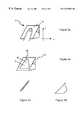
- FIG. 3 ashown is a perspective view of the prism 2 of FIG. 1 .
- An image of a fingerprint presented on the platen 12is distorted along both the x-axis and y-axis directions and hence it is necessary to correct perspective distortion for both the x-axis and y-axis directions.
- the x-axis and y-axisdefine different scan lines on the platen 12 .
- a scan lineis any series of adjacent data points on the platen 12 .
- FIG. 3 bshown is a perspective of a modified prism 35 of the present invention.
- the modified prismhas an output port 44 . It has been found that by having a recess with a correctly contoured surface it is possible to reduce perspective distortion by approximately 96%. Borders of the recess are in the shape of a triangle with rounded corners. The image of an object touching the surface of the platen 12 along line A is reduced in the x-axis to a lesser extent than an object along line B. Therefore, a fingerprint placed on the platen 12 is corrected for perspective size difference between the portion at the top of the platen 12 and that portion at the bottom of the platen 12 . Similarly, as shown in FIG. 3 c , it is possible to provide a modification to the output ports of the multi-prism 30 such perspective distortion is significantly eliminated.
- FIG. 3 danother prism for performing perspective distortion correction is shown.
- the imageis expanded along the vertical axis.
- correctionis performed by other than a spherical or cylindrical surface contour.
- the prism of FIG. 3 bis used because it reduces the necessary material for manufacturing the prism, reduces the area of the image sensor and so forth. Since the optics of the prism are analogue, there are substantial advantages to reducing overall image size.
- FIG. 3 ean image of a grid imaged through an optical component according to the invention is shown.
- the grid elementsappear near square and an equal number of squares is shown across each row.
- Optical geometry of optical fingerprint-imaging devices and principles governing themare known. These allow determination of perspective distortion. It has now been found that it is possible to correct for some of the perspective distortion resulting from optical contact imaging of for example fingerprints. As one skilled in the art will appreciate the nature of light and optics are well understood. In particular, it is possible to calculate the shape of a lens or the shape of a contoured reflective surface for incorporation into an optical fingerprint-imaging device for a predetermined correction of distortion. It is possible to compensate for perspective distortion by changing the shape of the output port 9 and/or the platen 12 such that it directs light from the platen in accordance with a substantially undistorted image of a biometric surface presented to the platen.
- a perspective correction optical componenthas a complex surface in comparison to a planar, spherical and/or cylindrical lens or shaped surface.
- a reason for the complex surfaceis that a perspective correction at a particular location on a scan line is not uniformly applied to all other scan lines.
- An evenly curved or cylindrically shaped surfaceapplies a substantially uniform correction. In this regard, an evenly curved or cylindrically shaped surface is not suitable for applying a perspective correction to an optical fingerprint-imaging device.
- a perspective correction optical component of the present inventionhas a complex three-dimensional contour.
- the complex contouris describable by a set of equations.
- the surfaceis a smoothly curved surface defined, 1 for example, by a hyberbolic function.
- a more sophisticated equation/functionis required to describe the contours of the perspective correction optical component.
- the complex contours of a perspective correction optical componenthave non-planar, non spherical and non-cylindrical contours that vary smoothly in three dimensions.
- FIG. 4shown is a side view of another modified prism 40 of the present invention.
- the modified prism 40has a platen 12 having a recess 46 therein.
- the recess 46allows a fingertip to contact more easily the platen surface 12 over prior art flat platens.
- An output port 9is shown as a corrective contoured recess 44 such as that shown in FIG. 3 b .
- the output port 9is a corrective contoured protrusion such as that shown in FIG. 3 d .
- either the corrective recess 44 or a corrective recess 46 or bothis present and reduces perspective distortion.
- each output port of a staircase-shaped prism 28 along with the platen surface 12it is possible to modify each output port of a staircase-shaped prism 28 along with the platen surface 12 to provide a perspective correction for a desired platen surface contour.
- FIG. 5shown is a side view of an optical fingerprint-imaging device of the present invention.
- Lightemerges from the output port 9 in a similar manner as described in FIG. 1 .
- the lightis incident on a shaped reflective surface 50 , which corrects for perspective distortion before light is incident on the detector.
- the shaped reflective surface 50is non-spherical and non-cylindrical.
- the reason for a non-spherical and non-cylindrical reflective surfaceis the same as mentioned above, namely, a perspective correction at a particular location on a scan line is not uniformly applied to all other scan lines.
- An evenly curved or cylindrically shaped surfaceapplies a substantially uniform correction.
- FIG. 6shown is a side view of an optical fingerprint-imaging device of the present invention.
- Lightemerges from the output port 9 in a similar manner as described in FIG. 1 .
- the lightis incident on a contoured lens 60 , which corrects for perspective distortion before light is incident on the image sensor 8 .
- the contoured lens 60is non-spherical and non-cylindrical as detailed above.
- an optical imaging devicehaving multiple lenses which are associated with respective CCDs is shown.
- the optical path between the lenses and the CCDsis shortened.
- a multi-prismis shown in combination with the multiple lens and multiple CCD arrangement.
- Perspective distortionis reduced by incorporating a plurality of contoured lens, or by incorporating a plurality of contoured reflective surfaces as shown.
- the resulting contact imagersupports high resolution imaging with reduced optical path length and simplified correction of optical perspective distortion since correction is required for a smaller perspective distortion within each image portion than exists across the entire imaged area.
- An optical fingerprint-imaging device having a perspective distortion correctionhas a single corrective optic or a plurality of corrective optics.
- the present inventionalso extents to a method for determining a perspective distortion correction for application to an optical fingerprint-imaging device.
- the geometry of an optical fingerprint-imaging deviceis known, for example, referring again to FIG. 1, distances d 1 , d 2 , angles ⁇ and ⁇ , and the dimensions of the lens 6 are known, as are any additional optical components present.
- Knowledge of the geometry of an optical fingerprint-imaging devicepermits calculation of geometry for additional optical components or of geometry for modifications required to result in correction of perspective distortion.
- predetermining a required correction of perspective distortionit is possible to manufacture economically viable components, for example, by form molding.
- the molding cost of an optical reading componentis far less than removing material from an existing optical reading component.
- a platen 12is shown with a grid of points disposed thereon.
- the gridis evenly spaced along the x and y axes. Alternatively, other spacing is also possible when design requirements dictate.
- An image sensor in the form of a CCD arrayis shown wherein each element within the array corresponds to a point on the grid of points shown on the platen 12 .
- an erroris determined between an actual target location on the image sensor surface and the target location selected for the point on the platen 12 .
- This errorrelates to distortion within the image corrective optics are disposed between the platen and the image sensor in order to correct the location of the point. When this is performed for all points, distortion is substantially minimised.
- FIG. 9a simplified flow diagram of a method of performing distortion correction is shown.
- An approach for designing a corrective modification having a smooth contour for the prism output port 9is to examine first a single linear scan line 12 a on the platen 12 and its corresponding array elements 8 a on the image sensor 8 . Commonly the associated elements are linear or near linear but this need not be so.
- a function that closely models the optically corrective surfaceis determined for the single scan line 12 a such that light therefrom is provided to predetermined positions 8 a on the image sensor 8 . This results in an image of the scan line that is corrected for perspective distortion and, when desirable, for other forms of distortion, and the function describes an optical surface to correct for the distortion.
- a single horizontal scan linehas a corrective function in the form of a hyperbolic function. The hyperbolic function in effect describes a “slice” through a corrective optical component.
- the hyperbolic functioncontains a plurality parameters, typically four or five parameters. It is assumed that the hyperbolic function is applicable as a corrective equation for a neighbouring scan line but with variations in the parameters. The parameters are varied within predetermined limits to determine another hyperbolic equation for correcting perspective distortion of the neighbouring scan line. The predetermined limits of the parameters serve to prevent discontinuity in a described surface. When sufficient neighbouring scan lines have been examined and their hyperbolic functions determined a continuous surface is described.
- the hyperbolic functions that describe the continuous surfaceprovide an optical surface function.
- the continuous surfacedescribes an optical surface that corrects for perspective distortion. It is possible for the optical surface to describe a recessed platen 44 , an optical modification to the output port 9 , a corrective lens 60 , or a corrective reflective surface 50 .
- a first reading coordinate on the platenis correlated to an image point on the image sensor and the process repeated a number of times.
- a two dimensional relationshipis determined between the reading coordinates on the platen and image points on the image sensor.
- Contours of an optical surfaceare determined for perturbing the light such that light reflecting from a predetermined point on the platen is incident on a predetermined point on the image sensor surface.
- Parameter arelates to depth of cut and as such is related to design choices and overall prism size parameter
- brelates to c, d, and e as shown in the second equation and is based on hyperbolic correction of distortion and so forth. Since these parameters are modified with each scan line, a smooth transition between adjacent hyperbolic functions can be maintained while correcting much of the perspective distortion within an image captured using the contact imager of the present invention. Numerous other embodiments may be envisaged without departing from the spirit and scope of the invention.
Landscapes
- Engineering & Computer Science (AREA)
- Physics & Mathematics (AREA)
- Optics & Photonics (AREA)
- Human Computer Interaction (AREA)
- General Physics & Mathematics (AREA)
- Multimedia (AREA)
- Theoretical Computer Science (AREA)
- Image Input (AREA)
Abstract
Description
Claims (19)
Priority Applications (1)
| Application Number | Priority Date | Filing Date | Title |
|---|---|---|---|
| US09/267,615US6373969B1 (en) | 1999-03-15 | 1999-03-15 | Corrective optical component |
Applications Claiming Priority (1)
| Application Number | Priority Date | Filing Date | Title |
|---|---|---|---|
| US09/267,615US6373969B1 (en) | 1999-03-15 | 1999-03-15 | Corrective optical component |
Publications (1)
| Publication Number | Publication Date |
|---|---|
| US6373969B1true US6373969B1 (en) | 2002-04-16 |
Family
ID=23019517
Family Applications (1)
| Application Number | Title | Priority Date | Filing Date |
|---|---|---|---|
| US09/267,615Expired - Fee RelatedUS6373969B1 (en) | 1999-03-15 | 1999-03-15 | Corrective optical component |
Country Status (1)
| Country | Link |
|---|---|
| US (1) | US6373969B1 (en) |
Cited By (63)
| Publication number | Priority date | Publication date | Assignee | Title |
|---|---|---|---|---|
| US20040109591A1 (en)* | 2002-12-06 | 2004-06-10 | Cross Match Technologies, Inc. | System for obtaining print and other hand characteristic information using a non-planar prism |
| US20040193539A1 (en)* | 2000-02-23 | 2004-09-30 | Bank One Corporation | Mutual fund card method and system |
| WO2004052173A3 (en)* | 2002-12-06 | 2004-10-21 | Cross Match Technologies Inc | System and a non-planar prism that are used to obtain print and other hand characteristic information |
| US20050105078A1 (en)* | 2003-10-09 | 2005-05-19 | Carver John F. | Palm print scanner and methods |
| US20060015743A1 (en)* | 2004-07-15 | 2006-01-19 | Anakam L.L.C. | System and method for blocking unauthorized network log in using stolen password |
| US20060069921A1 (en)* | 2004-07-15 | 2006-03-30 | Allan Camaisa | System and method for blocking unauthorized network log in using stolen password |
| US20060093192A1 (en)* | 2004-11-03 | 2006-05-04 | Bechtel J S | Finger guide device |
| US7051925B2 (en) | 2001-08-13 | 2006-05-30 | Bankone Delaware, N.A. | System and method for funding a collective account by use of an electronic tag |
| US20060133651A1 (en)* | 2002-12-31 | 2006-06-22 | Polcha Andrew J | Recoverable biometric identity system and method |
| US7072864B2 (en) | 1998-11-17 | 2006-07-04 | Bank One Deleware, N.A. | Customer activated multi-value (CAM) card |
| US7086586B1 (en) | 2003-08-13 | 2006-08-08 | Bank One, Delaware, National Association | System and method for a card payment program providing mutual benefits to card issuers and cardholders based on financial performance |
| US7099850B1 (en) | 2001-09-21 | 2006-08-29 | Jpmorgan Chase Bank, N.A. | Methods for providing cardless payment |
| US7103576B2 (en) | 2001-09-21 | 2006-09-05 | First Usa Bank, Na | System for providing cardless payment |
| US7130828B2 (en) | 1998-06-22 | 2006-10-31 | Jpmorgan Chase Bank, N.A. | Debit purchasing of stored value card for use by and/or delivery to others |
| US7165049B2 (en) | 2000-02-09 | 2007-01-16 | Jpmorgan Chase Bank, N.A. | Sponsor funded stored value card |
| US20070058844A1 (en)* | 2005-09-06 | 2007-03-15 | Fenrich Richard K | System and method for implementing algorithmic correction of image distortion within a fingerprint imaging system |
| US7191952B2 (en) | 2000-12-06 | 2007-03-20 | Jpmorgan Chase Bank, N.A. | Selectable multi-purpose card |
| US7260549B2 (en) | 2000-04-07 | 2007-08-21 | Jpmorgan Chase Bank, N.A. | Method and system for managing risk |
| US20070266257A1 (en)* | 2004-07-15 | 2007-11-15 | Allan Camaisa | System and method for blocking unauthorized network log in using stolen password |
| US7306141B1 (en) | 2001-08-13 | 2007-12-11 | Jpmorgan Chase Bank, N.A. | System and method for funding a collective account by use of an electronic tag |
| US20080086402A1 (en)* | 1999-11-15 | 2008-04-10 | The Chase Manhattan Bank | Personalized Interactive Network Architecture |
| US20080115981A1 (en)* | 2004-11-03 | 2008-05-22 | Bechtel J Scott | Finger guide device for use with stylus or pen |
| US7392222B1 (en) | 2004-08-03 | 2008-06-24 | Jpmorgan Chase Bank, N.A. | System and method for providing promotional pricing |
| US7401731B1 (en) | 2005-05-27 | 2008-07-22 | Jpmorgan Chase Bank, Na | Method and system for implementing a card product with multiple customized relationships |
| US7433829B2 (en) | 2000-12-12 | 2008-10-07 | Jpmorgan Chase Bank, N.A. | System and method for managing global risk |
| US20080250477A1 (en)* | 2004-07-15 | 2008-10-09 | Anakam Inc. | System and method for second factor authentication services |
| US7467106B1 (en) | 2004-06-18 | 2008-12-16 | Jpmorgan Chase Bank, N.A. | System and method for offer management |
| US7499887B2 (en) | 1999-06-04 | 2009-03-03 | Jpmorgan Chase Bank, N.A. | System and method for card processing with automated payment of club, merchant, and service provider fees |
| US7505918B1 (en) | 2006-05-26 | 2009-03-17 | Jpmorgan Chase Bank | Method and system for managing risks |
| US7512566B1 (en) | 2001-12-11 | 2009-03-31 | Jpmorgan Chase Bank, N.A. | System and method for using a stored value account having subaccount feature |
| US20090259848A1 (en)* | 2004-07-15 | 2009-10-15 | Williams Jeffrey B | Out of band system and method for authentication |
| USD602522S1 (en) | 2008-02-21 | 2009-10-20 | Jpmorgan Chase Bank, N.A. | Transaction device |
| US7660763B1 (en) | 1998-11-17 | 2010-02-09 | Jpmorgan Chase Bank, N.A. | Customer activated multi-value (CAM) card |
| US7676425B1 (en) | 2002-07-29 | 2010-03-09 | Jpmorgan Chase Bank, N.A. | Method and system for providing flexible financing |
| US20100100967A1 (en)* | 2004-07-15 | 2010-04-22 | Douglas James E | Secure collaborative environment |
| US7747463B1 (en) | 1998-06-22 | 2010-06-29 | Jpmorgan Chase Bank, N.A. | Debit purchasing of stored value card for use by and/or delivery to others |
| US7756896B1 (en) | 2002-03-11 | 2010-07-13 | Jp Morgan Chase Bank | System and method for multi-dimensional risk analysis |
| US7753259B1 (en) | 2006-04-13 | 2010-07-13 | Jpmorgan Chase Bank, N.A. | System and method for granting promotional rewards to both customers and non-customers |
| US7784682B2 (en) | 2006-02-08 | 2010-08-31 | Jpmorgan Chase Bank, N.A. | System and method for granting promotional rewards to both customers and non-customers |
| US7801816B2 (en) | 2001-05-23 | 2010-09-21 | Jp Morgan Chase Bank, N.A. | System and method for currency selectable stored value instrument |
| US7809641B2 (en) | 2001-07-26 | 2010-10-05 | Jpmorgan Chase Bank, National Association | System and method for funding a collective account |
| US7809595B2 (en) | 2002-09-17 | 2010-10-05 | Jpmorgan Chase Bank, Na | System and method for managing risks associated with outside service providers |
| US7860789B2 (en) | 2001-07-24 | 2010-12-28 | Jpmorgan Chase Bank, N.A. | Multiple account advanced payment card and method of routing card transactions |
| US7899753B1 (en) | 2002-03-25 | 2011-03-01 | Jpmorgan Chase Bank, N.A | Systems and methods for time variable financial authentication |
| US7953663B1 (en) | 2003-09-04 | 2011-05-31 | Jpmorgan Chase Bank, N.A. | System and method for financial instrument pre-qualification and offering |
| US8020754B2 (en) | 2001-08-13 | 2011-09-20 | Jpmorgan Chase Bank, N.A. | System and method for funding a collective account by use of an electronic tag |
| US8145549B2 (en) | 2003-05-30 | 2012-03-27 | Jpmorgan Chase Bank, N.A. | System and method for offering risk-based interest rates in a credit instutment |
| US8239323B2 (en) | 2003-09-23 | 2012-08-07 | Jpmorgan Chase Bank, N.A. | Method and system for distribution of unactivated bank account cards |
| US8408455B1 (en) | 2006-02-08 | 2013-04-02 | Jpmorgan Chase Bank, N.A. | System and method for granting promotional rewards to both customers and non-customers |
| US8417601B1 (en) | 2007-10-18 | 2013-04-09 | Jpmorgan Chase Bank, N.A. | Variable rate payment card |
| US8429006B1 (en) | 2004-06-18 | 2013-04-23 | Jpmorgan Chase Bank, N.A. | System and method for offer targeting |
| US8630898B1 (en) | 2005-02-22 | 2014-01-14 | Jpmorgan Chase Bank, N.A. | Stored value card provided with merchandise as rebate |
| US8676642B1 (en) | 2007-07-05 | 2014-03-18 | Jpmorgan Chase Bank, N.A. | System and method for granting promotional rewards to financial account holders |
| US8719085B2 (en) | 2001-01-18 | 2014-05-06 | Jpmorgan Chase Bank, N.A. | System and method for administering a brokerage rebate card program |
| US8751391B2 (en) | 2002-03-29 | 2014-06-10 | Jpmorgan Chase Bank, N.A. | System and process for performing purchase transactions using tokens |
| US8781905B2 (en) | 2000-08-01 | 2014-07-15 | Jpmorgan Chase Bank, N.A. | System and method for transponder-enabled account transactions |
| US8793160B2 (en) | 1999-12-07 | 2014-07-29 | Steve Sorem | System and method for processing transactions |
| US8800857B1 (en) | 2001-08-13 | 2014-08-12 | Jpmorgan Chase Bank, N.A. | System and method for crediting loyalty program points and providing loyalty rewards by use of an electronic tag |
| US9990642B2 (en) | 2002-10-11 | 2018-06-05 | Jpmorgan Chase Bank, N.A. | System and method for granting promotional rewards to credit account holders |
| US10282536B1 (en) | 2002-03-29 | 2019-05-07 | Jpmorgan Chase Bank, N.A. | Method and system for performing purchase and other transactions using tokens with multiple chips |
| US10438043B2 (en)* | 2015-08-14 | 2019-10-08 | Fujian Landi Commercial Equipment Co., Ltd. | Method and system for identifying fingerprint |
| US10726417B1 (en) | 2002-03-25 | 2020-07-28 | Jpmorgan Chase Bank, N.A. | Systems and methods for multifactor authentication |
| US10742416B2 (en) | 2017-08-21 | 2020-08-11 | Andrew J. Polcha | Fuzzy dataset processing and biometric identity technology leveraging blockchain ledger technology |
Citations (4)
| Publication number | Priority date | Publication date | Assignee | Title |
|---|---|---|---|---|
| US3975711A (en)* | 1974-08-30 | 1976-08-17 | Sperry Rand Corporation | Real time fingerprint recording terminal |
| US4905293A (en)* | 1984-07-18 | 1990-02-27 | Nec Corporation | Image input device |
| US5177802A (en)* | 1990-03-07 | 1993-01-05 | Sharp Kabushiki Kaisha | Fingerprint input apparatus |
| US5963657A (en)* | 1996-09-09 | 1999-10-05 | Arete Associates | Economical skin-pattern-acquisition and analysis apparatus for access control; systems controlled thereby |
- 1999
- 1999-03-15USUS09/267,615patent/US6373969B1/ennot_activeExpired - Fee Related
Patent Citations (4)
| Publication number | Priority date | Publication date | Assignee | Title |
|---|---|---|---|---|
| US3975711A (en)* | 1974-08-30 | 1976-08-17 | Sperry Rand Corporation | Real time fingerprint recording terminal |
| US4905293A (en)* | 1984-07-18 | 1990-02-27 | Nec Corporation | Image input device |
| US5177802A (en)* | 1990-03-07 | 1993-01-05 | Sharp Kabushiki Kaisha | Fingerprint input apparatus |
| US5963657A (en)* | 1996-09-09 | 1999-10-05 | Arete Associates | Economical skin-pattern-acquisition and analysis apparatus for access control; systems controlled thereby |
Cited By (139)
| Publication number | Priority date | Publication date | Assignee | Title |
|---|---|---|---|---|
| US7805368B2 (en) | 1998-06-22 | 2010-09-28 | Jpmorgan Chase Bank, N.A. | Debit purchasing of stored value card for use by and/or delivery to others |
| US7747463B1 (en) | 1998-06-22 | 2010-06-29 | Jpmorgan Chase Bank, N.A. | Debit purchasing of stored value card for use by and/or delivery to others |
| US7171388B2 (en) | 1998-06-22 | 2007-01-30 | Jpmorgan Chase Bank, N.A. | Debit purchasing of stored value card for use by and/or delivery to others |
| US7174315B2 (en) | 1998-06-22 | 2007-02-06 | Jpmorgan Chase Bank, N.A. | Debit purchasing of stored value card for use by and/or deliveries to others |
| US7174314B2 (en) | 1998-06-22 | 2007-02-06 | Jpmorgan Chase Bank, N.A. | Debit purchasing of stored value card for use by and/or delivery to others |
| US7130828B2 (en) | 1998-06-22 | 2006-10-31 | Jpmorgan Chase Bank, N.A. | Debit purchasing of stored value card for use by and/or delivery to others |
| US8005756B2 (en) | 1998-06-22 | 2011-08-23 | Jpmorgan Chase Bank, N.A. | Debit purchasing of stored value card for use by and/or delivery to others |
| US7809642B1 (en) | 1998-06-22 | 2010-10-05 | Jpmorgan Chase Bank, N.A. | Debit purchasing of stored value card for use by and/or delivery to others |
| US7174316B2 (en) | 1998-06-22 | 2007-02-06 | Jpmorgan Chase Bank, N.A. | Debit purchasing of stored value card for use by and/or delivery to others |
| US7809643B2 (en) | 1998-06-22 | 2010-10-05 | Jpmorgan Chase Bank, N.A. | Debit purchasing of stored value card for use by and/or delivery to others |
| US7174317B2 (en) | 1998-06-22 | 2007-02-06 | Jpmorgan Chase Bank, N.A. | Debit purchasing of stored value card for use by and/or delivery to others |
| US7818253B2 (en) | 1998-06-22 | 2010-10-19 | Jpmorgan Chase Bank, N.A. | Debit purchasing of stored value card for use by and/or delivery to others |
| US7363273B2 (en) | 1998-06-22 | 2008-04-22 | Jpmorgan Chase Bank, N.A. | Debit purchasing of stored value card for use by and/or delivery to others |
| US7660763B1 (en) | 1998-11-17 | 2010-02-09 | Jpmorgan Chase Bank, N.A. | Customer activated multi-value (CAM) card |
| US7263507B1 (en) | 1998-11-17 | 2007-08-28 | Jp Morgan Chase Bank, N.A. | Customer activated multi-value (CAM) card |
| US20080021826A1 (en)* | 1998-11-17 | 2008-01-24 | Brake Francis B Jr | Customer Activated Multi-Value (CAM) Card |
| US7072864B2 (en) | 1998-11-17 | 2006-07-04 | Bank One Deleware, N.A. | Customer activated multi-value (CAM) card |
| US7707111B2 (en) | 1998-11-17 | 2010-04-27 | Jpmorgan Chase Bank, N.A. | Customer activated multi-value (CAM) card |
| US7801799B1 (en) | 1998-11-17 | 2010-09-21 | Jpmorgan Chase Bank, N.A. | Customer activated multi-value (CAM) card |
| US8645265B2 (en) | 1999-06-04 | 2014-02-04 | Jpmorgan Chase Bank, N.A. | System and method for card processing with automated payment of club, merchant, and service provider fees |
| US7499887B2 (en) | 1999-06-04 | 2009-03-03 | Jpmorgan Chase Bank, N.A. | System and method for card processing with automated payment of club, merchant, and service provider fees |
| US7676429B2 (en) | 1999-06-04 | 2010-03-09 | Jpmorgan Chase Bank, N.A. | Credit instrument and system providing multiple services including access to credit services and access to a service provider club |
| US8326694B2 (en) | 1999-11-15 | 2012-12-04 | Jpmorgan Chase Bank, N.A. | Personalized interactive network architecture |
| US7949574B2 (en) | 1999-11-15 | 2011-05-24 | Jpmorgan Chase Bank, Na | Personalized interactive network architecture |
| US7370004B1 (en) | 1999-11-15 | 2008-05-06 | The Chase Manhattan Bank | Personalized interactive network architecture |
| US20080086402A1 (en)* | 1999-11-15 | 2008-04-10 | The Chase Manhattan Bank | Personalized Interactive Network Architecture |
| US9978089B2 (en) | 1999-11-15 | 2018-05-22 | Jpmorgan Chase, N.A. | Personalized interactive network with multiple channels coupled to integrated knowledge management system |
| US8793160B2 (en) | 1999-12-07 | 2014-07-29 | Steve Sorem | System and method for processing transactions |
| US7165049B2 (en) | 2000-02-09 | 2007-01-16 | Jpmorgan Chase Bank, N.A. | Sponsor funded stored value card |
| US20040193539A1 (en)* | 2000-02-23 | 2004-09-30 | Bank One Corporation | Mutual fund card method and system |
| US8700529B2 (en) | 2000-02-23 | 2014-04-15 | Jpmorgan Chase Bank, N.A. | Mutual fund card method and system |
| US8612341B2 (en) | 2000-02-23 | 2013-12-17 | Jpmorgan Chase Bank, N.A. | Computerized funding of a second financial account by a first financial card |
| US7603283B1 (en) | 2000-04-07 | 2009-10-13 | Jpmorgan Chase Bank, N.A. | Method and system for managing risk |
| US7260549B2 (en) | 2000-04-07 | 2007-08-21 | Jpmorgan Chase Bank, N.A. | Method and system for managing risk |
| US8781905B2 (en) | 2000-08-01 | 2014-07-15 | Jpmorgan Chase Bank, N.A. | System and method for transponder-enabled account transactions |
| US7591416B2 (en) | 2000-12-06 | 2009-09-22 | Jpmorgan Chase Bank, N.A. | Selectable multi-purpose card |
| US7357331B2 (en) | 2000-12-06 | 2008-04-15 | Jpmorgan Chase Bank, N.A. | Selectable multi-purpose card |
| US7191952B2 (en) | 2000-12-06 | 2007-03-20 | Jpmorgan Chase Bank, N.A. | Selectable multi-purpose card |
| US7433829B2 (en) | 2000-12-12 | 2008-10-07 | Jpmorgan Chase Bank, N.A. | System and method for managing global risk |
| US8719085B2 (en) | 2001-01-18 | 2014-05-06 | Jpmorgan Chase Bank, N.A. | System and method for administering a brokerage rebate card program |
| US7801816B2 (en) | 2001-05-23 | 2010-09-21 | Jp Morgan Chase Bank, N.A. | System and method for currency selectable stored value instrument |
| US7890422B1 (en) | 2001-07-24 | 2011-02-15 | Jpmorgan Chase Bank, N.A. | Multiple account advanced payment card and method of routing card transactions |
| US8751383B2 (en) | 2001-07-24 | 2014-06-10 | Jpmorgan Chase Bank, N.A. | Multiple account advanced payment card and method of routing card transactions |
| US7860789B2 (en) | 2001-07-24 | 2010-12-28 | Jpmorgan Chase Bank, N.A. | Multiple account advanced payment card and method of routing card transactions |
| US8515868B2 (en) | 2001-07-24 | 2013-08-20 | Jpmorgan Chase Bank, N.A. | Multiple account advanced payment card and method of routing card transactions |
| US7809641B2 (en) | 2001-07-26 | 2010-10-05 | Jpmorgan Chase Bank, National Association | System and method for funding a collective account |
| US8033451B2 (en) | 2001-08-13 | 2011-10-11 | Jpmorgan Chase Bank, National Association | System and method for funding a collective account by use of an electronic tag |
| US7311244B1 (en) | 2001-08-13 | 2007-12-25 | Jpmorgan Chase Bank, N.A. | System and method for funding a collective account by use of an electronic tag |
| US8020754B2 (en) | 2001-08-13 | 2011-09-20 | Jpmorgan Chase Bank, N.A. | System and method for funding a collective account by use of an electronic tag |
| US8800857B1 (en) | 2001-08-13 | 2014-08-12 | Jpmorgan Chase Bank, N.A. | System and method for crediting loyalty program points and providing loyalty rewards by use of an electronic tag |
| US7051925B2 (en) | 2001-08-13 | 2006-05-30 | Bankone Delaware, N.A. | System and method for funding a collective account by use of an electronic tag |
| US7349866B2 (en) | 2001-08-13 | 2008-03-25 | Jpmorgan Chase Bank, N.A. | System and method for funding a collective account by use of an electronic tag |
| US7306141B1 (en) | 2001-08-13 | 2007-12-11 | Jpmorgan Chase Bank, N.A. | System and method for funding a collective account by use of an electronic tag |
| US7103576B2 (en) | 2001-09-21 | 2006-09-05 | First Usa Bank, Na | System for providing cardless payment |
| US7099850B1 (en) | 2001-09-21 | 2006-08-29 | Jpmorgan Chase Bank, N.A. | Methods for providing cardless payment |
| US7512566B1 (en) | 2001-12-11 | 2009-03-31 | Jpmorgan Chase Bank, N.A. | System and method for using a stored value account having subaccount feature |
| US7756896B1 (en) | 2002-03-11 | 2010-07-13 | Jp Morgan Chase Bank | System and method for multi-dimensional risk analysis |
| US7899753B1 (en) | 2002-03-25 | 2011-03-01 | Jpmorgan Chase Bank, N.A | Systems and methods for time variable financial authentication |
| US10726417B1 (en) | 2002-03-25 | 2020-07-28 | Jpmorgan Chase Bank, N.A. | Systems and methods for multifactor authentication |
| US9240089B2 (en) | 2002-03-25 | 2016-01-19 | Jpmorgan Chase Bank, N.A. | Systems and methods for time variable financial authentication |
| US10282536B1 (en) | 2002-03-29 | 2019-05-07 | Jpmorgan Chase Bank, N.A. | Method and system for performing purchase and other transactions using tokens with multiple chips |
| US8751391B2 (en) | 2002-03-29 | 2014-06-10 | Jpmorgan Chase Bank, N.A. | System and process for performing purchase transactions using tokens |
| US8095459B2 (en) | 2002-07-29 | 2012-01-10 | Jpmorgan Chase Bank, N.A. | Method and system for providing flexible financing |
| US7676425B1 (en) | 2002-07-29 | 2010-03-09 | Jpmorgan Chase Bank, N.A. | Method and system for providing flexible financing |
| US8239304B1 (en) | 2002-07-29 | 2012-08-07 | Jpmorgan Chase Bank, N.A. | Method and system for providing pre-approved targeted products |
| US7809595B2 (en) | 2002-09-17 | 2010-10-05 | Jpmorgan Chase Bank, Na | System and method for managing risks associated with outside service providers |
| US10007923B1 (en) | 2002-10-11 | 2018-06-26 | Jpmorgan Chase Bank, N.A. | System and method for granting promotional rewards to credit account holders |
| US9990642B2 (en) | 2002-10-11 | 2018-06-05 | Jpmorgan Chase Bank, N.A. | System and method for granting promotional rewards to credit account holders |
| US7218761B2 (en) | 2002-12-06 | 2007-05-15 | Cross Match Technologies, Inc. | System for obtaining print and other hand characteristic information using a non-planar prism |
| US20060158751A1 (en)* | 2002-12-06 | 2006-07-20 | Cross Match Technologies, Inc. | Non-planar prism |
| US20040109245A1 (en)* | 2002-12-06 | 2004-06-10 | Cross Match Technologies, Inc. | Non-planar prism in a system for obtaining print and other hand characteristic information |
| US20040109589A1 (en)* | 2002-12-06 | 2004-06-10 | Cross Match Technologies, Inc. | System and method for generating a preview display in a print capturing system using a non-planar prism |
| US20040109591A1 (en)* | 2002-12-06 | 2004-06-10 | Cross Match Technologies, Inc. | System for obtaining print and other hand characteristic information using a non-planar prism |
| US20040114785A1 (en)* | 2002-12-06 | 2004-06-17 | Cross Match Technologies, Inc. | Methods for obtaining print and other hand characteristic information using a non-planar prism |
| US7190535B2 (en) | 2002-12-06 | 2007-03-13 | Cross Match Technologies, Inc. | Non-planar prism |
| US7321671B2 (en) | 2002-12-06 | 2008-01-22 | Cross Match Technologies, Inc. | System and method for generating a preview display in a print capturing system using a non-planar prism |
| US20040114786A1 (en)* | 2002-12-06 | 2004-06-17 | Cross Match Technologies, Inc. | System and method for capturing print information using a coordinate conversion method |
| US20040161136A1 (en)* | 2002-12-06 | 2004-08-19 | Cross Match Technologies, Inc. | System having a rotating optical system and a non-planar prism that are used to obtain print and other hand characteristic information |
| WO2004052173A3 (en)* | 2002-12-06 | 2004-10-21 | Cross Match Technologies Inc | System and a non-planar prism that are used to obtain print and other hand characteristic information |
| US6993165B2 (en) | 2002-12-06 | 2006-01-31 | Cross Match Technologies, Inc. | System having a rotating optical system and a non-planar prism that are used to obtain print and other hand characteristic information |
| US20060133651A1 (en)* | 2002-12-31 | 2006-06-22 | Polcha Andrew J | Recoverable biometric identity system and method |
| US8160307B2 (en)* | 2002-12-31 | 2012-04-17 | Polcha Andrew J | Recoverable biometric identity system and method |
| US20090175506A1 (en)* | 2002-12-31 | 2009-07-09 | Polcha Andrew J | Recoverable biometric identity system and method |
| US8306907B2 (en) | 2003-05-30 | 2012-11-06 | Jpmorgan Chase Bank N.A. | System and method for offering risk-based interest rates in a credit instrument |
| US8145549B2 (en) | 2003-05-30 | 2012-03-27 | Jpmorgan Chase Bank, N.A. | System and method for offering risk-based interest rates in a credit instutment |
| US7360693B1 (en) | 2003-08-13 | 2008-04-22 | Jpmorgan Chase Bank, N.A. | System and method for a card benefit program providing benefits to program members based on program performance |
| US7086586B1 (en) | 2003-08-13 | 2006-08-08 | Bank One, Delaware, National Association | System and method for a card payment program providing mutual benefits to card issuers and cardholders based on financial performance |
| US7953663B1 (en) | 2003-09-04 | 2011-05-31 | Jpmorgan Chase Bank, N.A. | System and method for financial instrument pre-qualification and offering |
| US8463681B2 (en) | 2003-09-23 | 2013-06-11 | Jpmorgan Chase Bank, N.A. | Method and system for distribution of unactivated bank account cards |
| US8239323B2 (en) | 2003-09-23 | 2012-08-07 | Jpmorgan Chase Bank, N.A. | Method and system for distribution of unactivated bank account cards |
| US7081951B2 (en) | 2003-10-09 | 2006-07-25 | Cross Match Technologies, Inc. | Palm print scanner and methods |
| US20050105078A1 (en)* | 2003-10-09 | 2005-05-19 | Carver John F. | Palm print scanner and methods |
| US8429006B1 (en) | 2004-06-18 | 2013-04-23 | Jpmorgan Chase Bank, N.A. | System and method for offer targeting |
| US7467106B1 (en) | 2004-06-18 | 2008-12-16 | Jpmorgan Chase Bank, N.A. | System and method for offer management |
| US10460341B2 (en) | 2004-06-18 | 2019-10-29 | Jpmorgan Chase Bank, N.A. | System and method for offer targeting |
| US8296562B2 (en) | 2004-07-15 | 2012-10-23 | Anakam, Inc. | Out of band system and method for authentication |
| US8219822B2 (en) | 2004-07-15 | 2012-07-10 | Anakam, Inc. | System and method for blocking unauthorized network log in using stolen password |
| US20100100967A1 (en)* | 2004-07-15 | 2010-04-22 | Douglas James E | Secure collaborative environment |
| US8079070B2 (en) | 2004-07-15 | 2011-12-13 | Anakam LLC | System and method for blocking unauthorized network log in using stolen password |
| US9047473B2 (en) | 2004-07-15 | 2015-06-02 | Anakam, Inc. | System and method for second factor authentication services |
| US20090259848A1 (en)* | 2004-07-15 | 2009-10-15 | Williams Jeffrey B | Out of band system and method for authentication |
| US7676834B2 (en) | 2004-07-15 | 2010-03-09 | Anakam L.L.C. | System and method for blocking unauthorized network log in using stolen password |
| US20080250477A1 (en)* | 2004-07-15 | 2008-10-09 | Anakam Inc. | System and method for second factor authentication services |
| US20070266257A1 (en)* | 2004-07-15 | 2007-11-15 | Allan Camaisa | System and method for blocking unauthorized network log in using stolen password |
| US20060015743A1 (en)* | 2004-07-15 | 2006-01-19 | Anakam L.L.C. | System and method for blocking unauthorized network log in using stolen password |
| US20060015742A1 (en)* | 2004-07-15 | 2006-01-19 | Allan Camaisa | System and method for blocking unauthorized network log in using stolen password |
| US20060069921A1 (en)* | 2004-07-15 | 2006-03-30 | Allan Camaisa | System and method for blocking unauthorized network log in using stolen password |
| US8533791B2 (en) | 2004-07-15 | 2013-09-10 | Anakam, Inc. | System and method for second factor authentication services |
| US8528078B2 (en) | 2004-07-15 | 2013-09-03 | Anakam, Inc. | System and method for blocking unauthorized network log in using stolen password |
| US8533111B1 (en) | 2004-08-03 | 2013-09-10 | Jpmorgan Chase Bank, N.A. | System and method for providing promotional pricing |
| US7392222B1 (en) | 2004-08-03 | 2008-06-24 | Jpmorgan Chase Bank, N.A. | System and method for providing promotional pricing |
| US9830493B2 (en) | 2004-11-03 | 2017-11-28 | Pen-One Acquisition Group, Llc | Finger guide device with capacitive sensor |
| US7929736B2 (en)* | 2004-11-03 | 2011-04-19 | Pen-One, Inc. | Finger guide device for use with stylus or pen |
| US20060093192A1 (en)* | 2004-11-03 | 2006-05-04 | Bechtel J S | Finger guide device |
| US9760753B2 (en) | 2004-11-03 | 2017-09-12 | Pen-One Acquisition Group, Llc | Finger guide device |
| US20080115981A1 (en)* | 2004-11-03 | 2008-05-22 | Bechtel J Scott | Finger guide device for use with stylus or pen |
| US8630898B1 (en) | 2005-02-22 | 2014-01-14 | Jpmorgan Chase Bank, N.A. | Stored value card provided with merchandise as rebate |
| US7401731B1 (en) | 2005-05-27 | 2008-07-22 | Jpmorgan Chase Bank, Na | Method and system for implementing a card product with multiple customized relationships |
| US7941355B1 (en) | 2005-05-27 | 2011-05-10 | Jpmorgan Chase Bank, N.A. | Universal payment protection |
| US8469265B2 (en) | 2005-05-27 | 2013-06-25 | Jpmorgan Chase Bank, N.A. | Method and system for implementing a card product with multiple customized relationships |
| US8752759B1 (en) | 2005-05-27 | 2014-06-17 | Jpmorgan Chase Bank, N.A. | Method and system for implementing a card product with multiple customized relationships |
| US8245909B2 (en) | 2005-05-27 | 2012-08-21 | Jpmorgan Chase Bank, Na | Method and system for implementing a card product with multiple customized relationships |
| US8925802B1 (en) | 2005-05-27 | 2015-01-06 | Jpmorgan Chase Bank, N.A. | Method and system for implementing a card product with multiple customized relationships |
| US8768013B2 (en)* | 2005-09-06 | 2014-07-01 | Identification International, Inc. | System and method for implementing algorithmic correction of image distortion within a fingerprint imaging system |
| US20070058844A1 (en)* | 2005-09-06 | 2007-03-15 | Fenrich Richard K | System and method for implementing algorithmic correction of image distortion within a fingerprint imaging system |
| US8068646B2 (en)* | 2005-09-06 | 2011-11-29 | Identification International, Inc. | System and method for implementing algorithmic correction of image distortion within a fingerprint imaging system |
| US7784682B2 (en) | 2006-02-08 | 2010-08-31 | Jpmorgan Chase Bank, N.A. | System and method for granting promotional rewards to both customers and non-customers |
| US8517258B2 (en) | 2006-02-08 | 2013-08-27 | Jpmorgan Chase Bank, N.A. | System and method for granting promotional rewards to both customers and non-customers |
| US8408455B1 (en) | 2006-02-08 | 2013-04-02 | Jpmorgan Chase Bank, N.A. | System and method for granting promotional rewards to both customers and non-customers |
| US7926711B2 (en) | 2006-02-08 | 2011-04-19 | Jpmorgan Chase Bank, N.A. | System and method for granting promotional rewards to both customers and non-customers |
| US7753259B1 (en) | 2006-04-13 | 2010-07-13 | Jpmorgan Chase Bank, N.A. | System and method for granting promotional rewards to both customers and non-customers |
| US7505918B1 (en) | 2006-05-26 | 2009-03-17 | Jpmorgan Chase Bank | Method and system for managing risks |
| US8676642B1 (en) | 2007-07-05 | 2014-03-18 | Jpmorgan Chase Bank, N.A. | System and method for granting promotional rewards to financial account holders |
| US8533086B1 (en) | 2007-10-18 | 2013-09-10 | Jpmorgan Chase Bank, N.A. | Variable rate payment card |
| US8417601B1 (en) | 2007-10-18 | 2013-04-09 | Jpmorgan Chase Bank, N.A. | Variable rate payment card |
| USD602522S1 (en) | 2008-02-21 | 2009-10-20 | Jpmorgan Chase Bank, N.A. | Transaction device |
| US10438043B2 (en)* | 2015-08-14 | 2019-10-08 | Fujian Landi Commercial Equipment Co., Ltd. | Method and system for identifying fingerprint |
| US10742416B2 (en) | 2017-08-21 | 2020-08-11 | Andrew J. Polcha | Fuzzy dataset processing and biometric identity technology leveraging blockchain ledger technology |
| US11444772B2 (en) | 2017-08-21 | 2022-09-13 | Andrew J. Polcha | Fuzzy dataset processing and biometric identity technology leveraging blockchain ledger technology |
Similar Documents
| Publication | Publication Date | Title |
|---|---|---|
| US6373969B1 (en) | Corrective optical component | |
| CN109255323B (en) | Fingerprint identification structure, display substrate and display device | |
| US6324020B1 (en) | Method and apparatus for reduction of trapezoidal distortion and improvement of image sharpness in an optical image capturing system | |
| US4322163A (en) | Finger identification | |
| US5233404A (en) | Optical scanning and recording apparatus for fingerprints | |
| US4720869A (en) | Hand dimension verification | |
| KR100429302B1 (en) | High contrast, low distortion optical acquisition system for image capturing | |
| US7952727B2 (en) | Compact optical contour digitizer | |
| KR100942081B1 (en) | Finger Detection Apparatus and Method Using Image Resampling | |
| EP3497618B1 (en) | Independently processing plurality of regions of interest | |
| US20110019243A1 (en) | Stereoscopic form reader | |
| US5090811A (en) | Optical radius gauge | |
| JP2000099711A (en) | Acquiring method for navigation position | |
| US11080511B2 (en) | Contactless rolled fingerprints | |
| US8068646B2 (en) | System and method for implementing algorithmic correction of image distortion within a fingerprint imaging system | |
| US11450140B2 (en) | Independently processing plurality of regions of interest | |
| US10091493B2 (en) | Device and method for scanning object outline image | |
| JPH1114327A (en) | Three-dimensional shape measuring method and device therefor | |
| US20070279617A1 (en) | Systems and methods of using a flexible imaging surface to capture a rolled fingerprint | |
| JP2568310B2 (en) | Physical feature input device | |
| EP0052348B1 (en) | Finger identification | |
| JPH0798764A (en) | Input device for fingerprint or palmprint or the like | |
| JP2906312B2 (en) | Input device | |
| EP1909063A1 (en) | Vision-measuring-machine calibration scale | |
| JPH0956U (en) | Image distortion measuring device for live scanner |
Legal Events
| Date | Code | Title | Description |
|---|---|---|---|
| AS | Assignment | Owner name:DEW ENGINEERING AND DEVELOPMENT LIMITED, CANADA Free format text:ASSIGNMENT OF ASSIGNORS INTEREST;ASSIGNOR:ADLER, ANDREW;REEL/FRAME:009830/0267 Effective date:19990311 | |
| AS | Assignment | Owner name:ACTIVCARD IRELAND, LIMITED, IRELAND Free format text:ASSIGNMENT OF ASSIGNORS INTEREST;ASSIGNOR:DEW ENGINEERING AND DEVELOPMENT LIMITED;REEL/FRAME:012567/0254 Effective date:20020124 | |
| FPAY | Fee payment | Year of fee payment:4 | |
| AS | Assignment | Owner name:ACTIVCARD CORP.,CALIFORNIA Free format text:LICENSE AGREEMENT;ASSIGNOR:DISCOBOLUS MANAGEMENT, LLC;REEL/FRAME:016547/0216 Effective date:20050606 Owner name:ACTIVCARD CORP., CALIFORNIA Free format text:LICENSE AGREEMENT;ASSIGNOR:DISCOBOLUS MANAGEMENT, LLC;REEL/FRAME:016547/0216 Effective date:20050606 | |
| FEPP | Fee payment procedure | Free format text:PAT HOLDER NO LONGER CLAIMS SMALL ENTITY STATUS, ENTITY STATUS SET TO UNDISCOUNTED (ORIGINAL EVENT CODE: STOL); ENTITY STATUS OF PATENT OWNER: LARGE ENTITY | |
| FPAY | Fee payment | Year of fee payment:8 | |
| REMI | Maintenance fee reminder mailed | ||
| LAPS | Lapse for failure to pay maintenance fees | ||
| STCH | Information on status: patent discontinuation | Free format text:PATENT EXPIRED DUE TO NONPAYMENT OF MAINTENANCE FEES UNDER 37 CFR 1.362 | |
| FP | Lapsed due to failure to pay maintenance fee | Effective date:20140416 |