US6373098B1 - Trench-gated device having trench walls formed by selective epitaxial growth and process for forming device - Google Patents
Trench-gated device having trench walls formed by selective epitaxial growth and process for forming deviceDownload PDFInfo
- Publication number
- US6373098B1 US6373098B1US09/318,334US31833499AUS6373098B1US 6373098 B1US6373098 B1US 6373098B1US 31833499 AUS31833499 AUS 31833499AUS 6373098 B1US6373098 B1US 6373098B1
- Authority
- US
- United States
- Prior art keywords
- layer
- trench
- substrate
- epitaxial material
- regions
- Prior art date
- Legal status (The legal status is an assumption and is not a legal conclusion. Google has not performed a legal analysis and makes no representation as to the accuracy of the status listed.)
- Expired - Lifetime
Links
Images


Classifications
- H—ELECTRICITY
- H10—SEMICONDUCTOR DEVICES; ELECTRIC SOLID-STATE DEVICES NOT OTHERWISE PROVIDED FOR
- H10D—INORGANIC ELECTRIC SEMICONDUCTOR DEVICES
- H10D30/00—Field-effect transistors [FET]
- H10D30/60—Insulated-gate field-effect transistors [IGFET]
- H10D30/64—Double-diffused metal-oxide semiconductor [DMOS] FETs
- H10D30/66—Vertical DMOS [VDMOS] FETs
- H—ELECTRICITY
- H10—SEMICONDUCTOR DEVICES; ELECTRIC SOLID-STATE DEVICES NOT OTHERWISE PROVIDED FOR
- H10D—INORGANIC ELECTRIC SEMICONDUCTOR DEVICES
- H10D64/00—Electrodes of devices having potential barriers
- H10D64/20—Electrodes characterised by their shapes, relative sizes or dispositions
- H10D64/27—Electrodes not carrying the current to be rectified, amplified, oscillated or switched, e.g. gates
- H10D64/291—Gate electrodes for thyristors
- H—ELECTRICITY
- H10—SEMICONDUCTOR DEVICES; ELECTRIC SOLID-STATE DEVICES NOT OTHERWISE PROVIDED FOR
- H10D—INORGANIC ELECTRIC SEMICONDUCTOR DEVICES
- H10D12/00—Bipolar devices controlled by the field effect, e.g. insulated-gate bipolar transistors [IGBT]
- H10D12/01—Manufacture or treatment
- H10D12/031—Manufacture or treatment of IGBTs
- H10D12/032—Manufacture or treatment of IGBTs of vertical IGBTs
- H10D12/038—Manufacture or treatment of IGBTs of vertical IGBTs having a recessed gate, e.g. trench-gate IGBTs
- H—ELECTRICITY
- H10—SEMICONDUCTOR DEVICES; ELECTRIC SOLID-STATE DEVICES NOT OTHERWISE PROVIDED FOR
- H10D—INORGANIC ELECTRIC SEMICONDUCTOR DEVICES
- H10D12/00—Bipolar devices controlled by the field effect, e.g. insulated-gate bipolar transistors [IGBT]
- H10D12/411—Insulated-gate bipolar transistors [IGBT]
- H10D12/441—Vertical IGBTs
- H10D12/461—Vertical IGBTs having non-planar surfaces, e.g. having trenches, recesses or pillars in the surfaces of the emitter, base or collector regions
- H10D12/481—Vertical IGBTs having non-planar surfaces, e.g. having trenches, recesses or pillars in the surfaces of the emitter, base or collector regions having gate structures on slanted surfaces, on vertical surfaces, or in grooves, e.g. trench gate IGBTs
- H—ELECTRICITY
- H10—SEMICONDUCTOR DEVICES; ELECTRIC SOLID-STATE DEVICES NOT OTHERWISE PROVIDED FOR
- H10D—INORGANIC ELECTRIC SEMICONDUCTOR DEVICES
- H10D30/00—Field-effect transistors [FET]
- H10D30/60—Insulated-gate field-effect transistors [IGFET]
- H10D30/64—Double-diffused metal-oxide semiconductor [DMOS] FETs
- H10D30/66—Vertical DMOS [VDMOS] FETs
- H10D30/668—Vertical DMOS [VDMOS] FETs having trench gate electrodes, e.g. UMOS transistors
- H—ELECTRICITY
- H10—SEMICONDUCTOR DEVICES; ELECTRIC SOLID-STATE DEVICES NOT OTHERWISE PROVIDED FOR
- H10D—INORGANIC ELECTRIC SEMICONDUCTOR DEVICES
- H10D64/00—Electrodes of devices having potential barriers
- H10D64/20—Electrodes characterised by their shapes, relative sizes or dispositions
- H10D64/23—Electrodes carrying the current to be rectified, amplified, oscillated or switched, e.g. sources, drains, anodes or cathodes
- H10D64/251—Source or drain electrodes for field-effect devices
- H10D64/256—Source or drain electrodes for field-effect devices for lateral devices wherein the source or drain electrodes are recessed in semiconductor bodies
Definitions
- the present inventionrelates to semiconductor devices and, more particularly, to a trench-gated device having trench walls formed by selective epitaxial growth and a process for making the device.
- the DMOS trench gatetypically includes a trench extending from the source to the drain and having sidewalls and a floor that are each lined with a layer of thermally grown silicon dioxide.
- the lined trenchis filled with doped polysilicon.
- the structure of the trench gateallows less constricted current flow and, consequently, provides lower values of specific on-resistance.
- the trench gatemakes possible a decreased cell pitch in an MOS channel extending along the vertical sidewalls of the trench from the bottom of the source across the body of the transistor to the drain below. Channel density is thereby increased, which reduces the contribution of the channel to on-resistance.
- trench DMOS transistorsThe structure and performance of trench DMOS transistors are discussed in Bulucea and Rossen, “Trench DMOS Transistor Technology for High-Current (100 A Range) Switching,” in Solid-State Electronics, 1991, Vol. 34, No. 5, pp 493-507, the disclosure of which is incorporated herein by reference.
- trench gatesare also advantageously employed in insulated gate bipolar transistors (IGBTs), MOS-controlled thyristors (MCTs), and other trench-gated devices.
- IGBTsinsulated gate bipolar transistors
- MCTsMOS-controlled thyristors
- a typical semiconductor devicecontains an array of MOSFET structures arranged in various cellular or stripe layouts currently used by the industry.
- the trench gate of a MOSFETis typically formed by plasma etching a trench into a substrate and lining the trench with a dielectric material prior to substantially filling it with a conductive material.
- the surface roughness of the etched trench sidewallbecomes increasingly important because of its effect on the threshold voltage and reliability of the device.
- the improved smoothness of the sidewalls in a device of the present inventionprovides an improvement in the efficiency and power handling capability of the device.
- the present inventionis directed to an improved trench-gated power device comprising a substrate having an overlying layer of epitaxial material disposed on an upper layer of the substrate, well regions containing source and body regions, a trench gate, and a drain region, wherein the improvement comprises a gate trench having beneficially smooth sidewalls that comprise selectively grown epitaxial material and body regions that are recessed with respect to adjacent source regions.
- a process for forming an improved trench-gated power deviceis a process for forming an improved trench-gated power device.
- a dielectric layer having an upper surface and thickness and width dimensions that substantially correspond to the height and width dimensions of a gate trenchis formed on an upper layer of a substrate.
- a layer of epitaxial materialis grown on the upper layer of the substrate and the dielectric layer and planarized to be substantially coplanar with the upper surface of the dielectric layer, which is then removed, thereby forming gate trench sidewalls that comprise selectively grown epitaxial material.
- the processfurther comprises lining the trench with a dielectric material and substantially filling the lined trench with a conductive material, thereby forming a trench gate, and forming well, body, and source regions in the planarized epitaxial material.
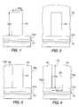
- FIGS. 1-6depict a process for forming a semiconductor device of the present alone invention.
- FIGS. 1-6schematically illustrate a process for forming a trench-gated device 100 of the present invention on a semiconductor substrate 101 , which can be N-doped monocrystalline silicon.
- Substrate 101includes an upper layer 101 a, which can be part of substrate 101 itself or; preferably, an epitaxial layer, of either N-type or P-type, that is thick enough to support breakdown voltage.
- a layer of dielectric materialis grown or deposited on substrate upper layer 101 a and masked and etched to form a dielectric layer 102 , which has thickness and width dimensions 102 t and 102 w, respectively, as shown in FIG. 1 .
- a plurality of dielectric layers 102are formed on the surface of substrate 101 .
- a layer 103 of epitaxial materialis grown on layers 101 a and 102 , as depicted in FIG. 2 . It is, of course, recognized that the dimensions of substrate 101 , dielectric layer 102 , epitaxial layer 103 , and other features as shown in the figures are not to scale but are distorted for increased clarity.
- Layer 103is planarized to layer 103 p, as shown in FIG. 3 .
- the thickness of layer 103 p adjacent to dielectric layer 102is substantially equal to 102 t but becomes thinner in region 104 away from dielectric layer 102 .
- Removal of layer 102 by a chemical etching procedureresults in the formation of a gate trench 105 having sidewalls 106 , as depicted in FIG. 4 .
- Chemical etching of layer 102may be carried out using, for example, an acidic agent such as hydrofluoric acid in a buffered oxide etch (BOE) process.
- Trench 105has height and width dimensions 105 h and 105 w, respectively, that substantially correspond to the dimensions 102 t and 102 w of dielectric layer 102 .
- Gate trench 105is lined with dielectric material 107 , which can be silicon dioxide, and substantially filled with a conductive material 108 such as doped polysilicon to form a trench gate 109 , as shown in FIG. 5.
- a surface cleaning stepcan optionally be employed prior to lining trench 105 with dielectric material 107 ; the trench lining process causes epitaxial layer 103 p to diffuse laterally and vertically around the comer of trench 105 , thereby mitigating possible trench comer-related reliability problems.
- the fabrication of device 100is completed by implantation and thermal activation/diffusion to form N+ source regions 110 and P+ body regions 111 .
- the lower portion of epitaxial layer 103 pserves as a P-well region 112 , and the lower portion of substrate 101 provides a drain region 113 .
- An interlevel dielectric layer 114is formed over source regions 110 and gate trench 109 , and metal layer 115 , which is in electrical contact with source and body regions 110 and 111 , respectively, is deposited over epitaxial layer 103 p and interlevel dielectric layer 114 .
- a metal layer(not shown) is also deposited on the lower surface of substrate 101 to provide a contact with drain region 113 .
- gate trench sidewalls 106are beneficially smoother than they would have been had gate trench 105 been formed by plasma etching. Also as noted above, because the epitaxial layer planarization procedure produces a thinner region 104 of planarized layer 103 p, body regions 111 of device 100 are recessed, which provides a potential advantage of increased contact area and improved unclamped inductive switching (UIS) capability.
- UISunclamped inductive switching
- the sequence of source and body region formation in relation to interlevel dielectric formationcan be altered without affecting the final device function and layout.
- a well regionis defined within the selectively grown P-type epitaxial layer, the uniformly doped well providing a good balance between on-resistance and short channel effects.
- the wellcan also be formed by selectively growing an N-type epitaxial layer, which is then doped by ion implantation and diffusion of a P-type dopant.
- the present inventionis illustrated using an N-channel silicon substrate, but it can also be applied to other devices and other dopants and other semiconductor materials, for example, silicon-germanium.
- the described deviceis a power MOSFET, but the invention is applicable to all trench-gated devices, for example, insulated gate bipolar transistors (IGBTs), MOS-controlled thyristors (MCTs), and the like.
- IGBTsinsulated gate bipolar transistors
- MCTsMOS-controlled thyristors
Landscapes
- Thyristors (AREA)
- Electrodes Of Semiconductors (AREA)
- Insulated Gate Type Field-Effect Transistor (AREA)
- Semiconductor Memories (AREA)
Abstract
Description
Claims (17)
Priority Applications (4)
| Application Number | Priority Date | Filing Date | Title |
|---|---|---|---|
| US09/318,334US6373098B1 (en) | 1999-05-25 | 1999-05-25 | Trench-gated device having trench walls formed by selective epitaxial growth and process for forming device |
| EP00110509AEP1056134A3 (en) | 1999-05-25 | 2000-05-17 | Trench-gated device having trench walls formed by selective epitaxial growth and process for forming the device |
| JP2000152488AJP4733247B2 (en) | 1999-05-25 | 2000-05-24 | Trench gate device with trench walls formed by selective epitaxial growth |
| KR1020000028310AKR100656239B1 (en) | 1999-05-25 | 2000-05-25 | Trench-gate power device with trench walls formed by selective epitaxial growth |
Applications Claiming Priority (1)
| Application Number | Priority Date | Filing Date | Title |
|---|---|---|---|
| US09/318,334US6373098B1 (en) | 1999-05-25 | 1999-05-25 | Trench-gated device having trench walls formed by selective epitaxial growth and process for forming device |
Publications (1)
| Publication Number | Publication Date |
|---|---|
| US6373098B1true US6373098B1 (en) | 2002-04-16 |
Family
ID=23237739
Family Applications (1)
| Application Number | Title | Priority Date | Filing Date |
|---|---|---|---|
| US09/318,334Expired - LifetimeUS6373098B1 (en) | 1999-05-25 | 1999-05-25 | Trench-gated device having trench walls formed by selective epitaxial growth and process for forming device |
Country Status (4)
| Country | Link |
|---|---|
| US (1) | US6373098B1 (en) |
| EP (1) | EP1056134A3 (en) |
| JP (1) | JP4733247B2 (en) |
| KR (1) | KR100656239B1 (en) |
Cited By (16)
| Publication number | Priority date | Publication date | Assignee | Title |
|---|---|---|---|---|
| US20020008284A1 (en)* | 2000-07-20 | 2002-01-24 | Fairchild Semiconductor Corporation | Power mosfet and method for forming same using a self-aligned body implant |
| US20020109135A1 (en)* | 2001-02-09 | 2002-08-15 | Junichi Murota | MOS field-effect transistor comprising layered structure including Si layer and SiGe layer OR SiGeC layer as channel regions |
| US7352036B2 (en) | 2004-08-03 | 2008-04-01 | Fairchild Semiconductor Corporation | Semiconductor power device having a top-side drain using a sinker trench |
| US7429523B2 (en) | 2001-10-17 | 2008-09-30 | Fairchild Semiconductor Corporation | Method of forming schottky diode with charge balance structure |
| US7504306B2 (en) | 2005-04-06 | 2009-03-17 | Fairchild Semiconductor Corporation | Method of forming trench gate field effect transistor with recessed mesas |
| US7582519B2 (en) | 2002-11-05 | 2009-09-01 | Fairchild Semiconductor Corporation | Method of forming a trench structure having one or more diodes embedded therein adjacent a PN junction |
| US7713822B2 (en) | 2006-03-24 | 2010-05-11 | Fairchild Semiconductor Corporation | Method of forming high density trench FET with integrated Schottky diode |
| US8110868B2 (en) | 2005-07-27 | 2012-02-07 | Infineon Technologies Austria Ag | Power semiconductor component with a low on-state resistance |
| US20120126341A1 (en)* | 2010-11-23 | 2012-05-24 | Microchip Technology Incorporated | Using low pressure epi to enable low rdson fet |
| CN103094116A (en)* | 2011-11-01 | 2013-05-08 | 上海华虹Nec电子有限公司 | Technique method of manufacturing groove metal oxide semiconductor (MOS) |
| US9166030B2 (en) | 2010-03-19 | 2015-10-20 | Fujitsu Limited | Compound semiconductor device and method for fabricating |
| US9190511B2 (en) | 2005-07-27 | 2015-11-17 | Infineon Technologies Austria Ag | Semiconductor component with a drift region and a drift control region |
| US9312373B2 (en) | 2010-07-14 | 2016-04-12 | Fujitsu Limited | Compound semiconductor device and manufacturing method of the same |
| CN109671766A (en)* | 2017-10-13 | 2019-04-23 | 联华电子股份有限公司 | Power metal-oxide-semiconductor field effect transistor |
| US20220293733A1 (en)* | 2020-07-21 | 2022-09-15 | IceMos Technology Limited | Radiation Hardened High Voltage Superjunction MOSFET |
| CN115084247A (en)* | 2022-08-22 | 2022-09-20 | 泰科天润半导体科技(北京)有限公司 | Manufacturing method of double-groove type silicon carbide MOSFET |
Families Citing this family (4)
| Publication number | Priority date | Publication date | Assignee | Title |
|---|---|---|---|---|
| US6246090B1 (en)* | 2000-03-14 | 2001-06-12 | Intersil Corporation | Power trench transistor device source region formation using silicon spacer |
| JP4826036B2 (en)* | 2001-07-16 | 2011-11-30 | 株式会社デンソー | Manufacturing method of semiconductor device |
| US9484451B2 (en)* | 2007-10-05 | 2016-11-01 | Vishay-Siliconix | MOSFET active area and edge termination area charge balance |
| JP2012104568A (en) | 2010-11-08 | 2012-05-31 | Sumitomo Electric Ind Ltd | Semiconductor device and method of manufacturing the same |
Citations (9)
| Publication number | Priority date | Publication date | Assignee | Title |
|---|---|---|---|---|
| US5378655A (en)* | 1993-04-01 | 1995-01-03 | U.S. Philips Corporation | Method of manufacturing a semiconductor device comprising an insulated gate field effect device |
| US5489787A (en)* | 1993-07-05 | 1996-02-06 | U.S. Philips Corporation | Semiconductor device having an insulated gate field effect transistor and exhibiting thyristor action |
| US5656843A (en)* | 1992-08-05 | 1997-08-12 | U.S. Philips Corporation | Semiconductor device having a vertical insulated gate field effect device and a breakdown region remote from the gate |
| US5844273A (en)* | 1994-12-09 | 1998-12-01 | Fuji Electric Co. | Vertical semiconductor device and method of manufacturing the same |
| US5864159A (en)* | 1994-12-13 | 1999-01-26 | Mitsubishi Denki Kabushiki Kaisha | Insulated gate semiconductor device structure to prevent a reduction in breakdown voltage |
| US5895951A (en)* | 1996-04-05 | 1999-04-20 | Megamos Corporation | MOSFET structure and fabrication process implemented by forming deep and narrow doping regions through doping trenches |
| US5929482A (en)* | 1997-10-31 | 1999-07-27 | Mitsubishi Denki Kabushiki Kaisha | Power semiconductor device and method for manufacturing the same |
| US5973367A (en)* | 1995-10-13 | 1999-10-26 | Siliconix Incorporated | Multiple gated MOSFET for use in DC-DC converter |
| US6091107A (en)* | 1997-01-21 | 2000-07-18 | Mitel Semiconductor Limited | Semiconductor devices |
Family Cites Families (9)
| Publication number | Priority date | Publication date | Assignee | Title |
|---|---|---|---|---|
| JPS60109278A (en)* | 1983-11-18 | 1985-06-14 | Hitachi Ltd | Semiconductor device |
| US5283201A (en)* | 1988-05-17 | 1994-02-01 | Advanced Power Technology, Inc. | High density power device fabrication process |
| JPH0360076A (en)* | 1989-07-27 | 1991-03-15 | Seiko Instr Inc | Manufacture of vertical field effect transistor |
| JP3647515B2 (en)* | 1995-08-28 | 2005-05-11 | 株式会社デンソー | Method for manufacturing p-type silicon carbide semiconductor |
| JPH09321296A (en)* | 1996-05-27 | 1997-12-12 | Toyota Central Res & Dev Lab Inc | Semiconductor device and manufacturing method thereof |
| KR100225409B1 (en)* | 1997-03-27 | 1999-10-15 | 김덕중 | Trench di-Moose and preparation method thereof |
| JPH10321848A (en)* | 1997-05-22 | 1998-12-04 | Nissan Motor Co Ltd | Method for manufacturing semiconductor device |
| US5955759A (en)* | 1997-12-11 | 1999-09-21 | International Business Machines Corporation | Reduced parasitic resistance and capacitance field effect transistor |
| JP3219045B2 (en)* | 1998-02-20 | 2001-10-15 | 日本電気株式会社 | Manufacturing method of vertical MISFET |
- 1999
- 1999-05-25USUS09/318,334patent/US6373098B1/ennot_activeExpired - Lifetime
- 2000
- 2000-05-17EPEP00110509Apatent/EP1056134A3/ennot_activeWithdrawn
- 2000-05-24JPJP2000152488Apatent/JP4733247B2/ennot_activeExpired - Lifetime
- 2000-05-25KRKR1020000028310Apatent/KR100656239B1/ennot_activeExpired - Lifetime
Patent Citations (9)
| Publication number | Priority date | Publication date | Assignee | Title |
|---|---|---|---|---|
| US5656843A (en)* | 1992-08-05 | 1997-08-12 | U.S. Philips Corporation | Semiconductor device having a vertical insulated gate field effect device and a breakdown region remote from the gate |
| US5378655A (en)* | 1993-04-01 | 1995-01-03 | U.S. Philips Corporation | Method of manufacturing a semiconductor device comprising an insulated gate field effect device |
| US5489787A (en)* | 1993-07-05 | 1996-02-06 | U.S. Philips Corporation | Semiconductor device having an insulated gate field effect transistor and exhibiting thyristor action |
| US5844273A (en)* | 1994-12-09 | 1998-12-01 | Fuji Electric Co. | Vertical semiconductor device and method of manufacturing the same |
| US5864159A (en)* | 1994-12-13 | 1999-01-26 | Mitsubishi Denki Kabushiki Kaisha | Insulated gate semiconductor device structure to prevent a reduction in breakdown voltage |
| US5973367A (en)* | 1995-10-13 | 1999-10-26 | Siliconix Incorporated | Multiple gated MOSFET for use in DC-DC converter |
| US5895951A (en)* | 1996-04-05 | 1999-04-20 | Megamos Corporation | MOSFET structure and fabrication process implemented by forming deep and narrow doping regions through doping trenches |
| US6091107A (en)* | 1997-01-21 | 2000-07-18 | Mitel Semiconductor Limited | Semiconductor devices |
| US5929482A (en)* | 1997-10-31 | 1999-07-27 | Mitsubishi Denki Kabushiki Kaisha | Power semiconductor device and method for manufacturing the same |
Cited By (29)
| Publication number | Priority date | Publication date | Assignee | Title |
|---|---|---|---|---|
| US6921939B2 (en)* | 2000-07-20 | 2005-07-26 | Fairchild Semiconductor Corporation | Power MOSFET and method for forming same using a self-aligned body implant |
| US20050184318A1 (en)* | 2000-07-20 | 2005-08-25 | Fairchild Semiconductor Corporation, State Of Incorporation: Delaware | Power mosfet and method for forming same using a self-aligned body implant |
| US7501323B2 (en) | 2000-07-20 | 2009-03-10 | Fairchild Semiconductor Corporation | Power MOSFET and method for forming same using a self-aligned body implant |
| US20020008284A1 (en)* | 2000-07-20 | 2002-01-24 | Fairchild Semiconductor Corporation | Power mosfet and method for forming same using a self-aligned body implant |
| US20020109135A1 (en)* | 2001-02-09 | 2002-08-15 | Junichi Murota | MOS field-effect transistor comprising layered structure including Si layer and SiGe layer OR SiGeC layer as channel regions |
| US7429523B2 (en) | 2001-10-17 | 2008-09-30 | Fairchild Semiconductor Corporation | Method of forming schottky diode with charge balance structure |
| US7582519B2 (en) | 2002-11-05 | 2009-09-01 | Fairchild Semiconductor Corporation | Method of forming a trench structure having one or more diodes embedded therein adjacent a PN junction |
| US8026558B2 (en) | 2004-08-03 | 2011-09-27 | Fairchild Semiconductor Corporation | Semiconductor power device having a top-side drain using a sinker trench |
| US7352036B2 (en) | 2004-08-03 | 2008-04-01 | Fairchild Semiconductor Corporation | Semiconductor power device having a top-side drain using a sinker trench |
| US8148233B2 (en) | 2004-08-03 | 2012-04-03 | Fairchild Semiconductor Corporation | Semiconductor power device having a top-side drain using a sinker trench |
| US7732876B2 (en) | 2004-08-03 | 2010-06-08 | Fairchild Semiconductor Corporation | Power transistor with trench sinker for contacting the backside |
| US7504306B2 (en) | 2005-04-06 | 2009-03-17 | Fairchild Semiconductor Corporation | Method of forming trench gate field effect transistor with recessed mesas |
| US8084327B2 (en) | 2005-04-06 | 2011-12-27 | Fairchild Semiconductor Corporation | Method for forming trench gate field effect transistor with recessed mesas using spacers |
| US8680611B2 (en) | 2005-04-06 | 2014-03-25 | Fairchild Semiconductor Corporation | Field effect transistor and schottky diode structures |
| US8110868B2 (en) | 2005-07-27 | 2012-02-07 | Infineon Technologies Austria Ag | Power semiconductor component with a low on-state resistance |
| US8643086B2 (en) | 2005-07-27 | 2014-02-04 | Infineon Technologies Austria Ag | Semiconductor component with high breakthrough tension and low forward resistance |
| US9190511B2 (en) | 2005-07-27 | 2015-11-17 | Infineon Technologies Austria Ag | Semiconductor component with a drift region and a drift control region |
| US7713822B2 (en) | 2006-03-24 | 2010-05-11 | Fairchild Semiconductor Corporation | Method of forming high density trench FET with integrated Schottky diode |
| US9166030B2 (en) | 2010-03-19 | 2015-10-20 | Fujitsu Limited | Compound semiconductor device and method for fabricating |
| US9337326B2 (en) | 2010-03-19 | 2016-05-10 | Fujitsu Limited | Compound semiconductor device and method for fabricating the same |
| US9515063B2 (en) | 2010-07-14 | 2016-12-06 | Fujitsu Limited | Compound semiconductor device and manufacturing method of the same |
| US9312373B2 (en) | 2010-07-14 | 2016-04-12 | Fujitsu Limited | Compound semiconductor device and manufacturing method of the same |
| US20120126341A1 (en)* | 2010-11-23 | 2012-05-24 | Microchip Technology Incorporated | Using low pressure epi to enable low rdson fet |
| CN103094116A (en)* | 2011-11-01 | 2013-05-08 | 上海华虹Nec电子有限公司 | Technique method of manufacturing groove metal oxide semiconductor (MOS) |
| CN109671766A (en)* | 2017-10-13 | 2019-04-23 | 联华电子股份有限公司 | Power metal-oxide-semiconductor field effect transistor |
| US20220293733A1 (en)* | 2020-07-21 | 2022-09-15 | IceMos Technology Limited | Radiation Hardened High Voltage Superjunction MOSFET |
| US11757001B2 (en)* | 2020-07-21 | 2023-09-12 | IceMos Technology Limited | Radiation hardened high voltage superjunction MOSFET |
| US12230674B2 (en) | 2020-07-21 | 2025-02-18 | IceMos Technology Limited | Radiation hardened high voltage superjunction MOSFET |
| CN115084247A (en)* | 2022-08-22 | 2022-09-20 | 泰科天润半导体科技(北京)有限公司 | Manufacturing method of double-groove type silicon carbide MOSFET |
Also Published As
| Publication number | Publication date |
|---|---|
| KR100656239B1 (en) | 2006-12-15 |
| JP4733247B2 (en) | 2011-07-27 |
| EP1056134A3 (en) | 2002-06-05 |
| EP1056134A2 (en) | 2000-11-29 |
| KR20000077429A (en) | 2000-12-26 |
| JP2000349092A (en) | 2000-12-15 |
Similar Documents
| Publication | Publication Date | Title |
|---|---|---|
| US7388254B2 (en) | MOS-gated device having a buried gate and process for forming same | |
| US6373098B1 (en) | Trench-gated device having trench walls formed by selective epitaxial growth and process for forming device | |
| US6365942B1 (en) | MOS-gated power device with doped polysilicon body and process for forming same | |
| US6198127B1 (en) | MOS-gated power device having extended trench and doping zone and process for forming same | |
| US8222693B2 (en) | Trench-gate transistors and their manufacture | |
| US5648283A (en) | High density power device fabrication process using undercut oxide sidewalls | |
| US6673681B2 (en) | Process for forming MOS-gated power device having segmented trench and extended doping zone | |
| US6638826B2 (en) | Power MOS device with buried gate | |
| US11239351B2 (en) | Semiconductor device with a LOCOS trench | |
| US20220320295A1 (en) | Sic mosfet structures with asymmetric trench oxide | |
| TWI475614B (en) | Ditch installation structure and manufacturing | |
| CN102347220A (en) | Trench superjunction mosfet with thin epi process | |
| US7439580B2 (en) | Top drain MOSgated device and process of manufacture therefor | |
| KR20120003019A (en) | Power semiconductor device and manufacturing method | |
| CN107112276A (en) | Power module with polysilicon filled trench with tapered oxide thickness | |
| US11652170B2 (en) | Trench field effect transistor structure free from contact hole | |
| US20240222480A1 (en) | Igbt device | |
| CN119562567A (en) | IGBT device and manufacturing method thereof | |
| CN108428742A (en) | A kind of superjunction trench MOS structure semiconductor device |
Legal Events
| Date | Code | Title | Description |
|---|---|---|---|
| AS | Assignment | Owner name:HARRIS CORPORATION, FLORIDA Free format text:ASSIGNMENT OF ASSIGNORS INTEREST;ASSIGNORS:BRUSH, LINDA S.;ZENG, JUN;KOCON, CHRISTOPHER B.;REEL/FRAME:009992/0801 Effective date:19990521 | |
| AS | Assignment | Owner name:INTERSIL CORPORATION, FLORIDA Free format text:AMEND TO ADD PROPERTIES RECORDED ON REEL 10247, FRAME 0043.;ASSIGNOR:HARRIS CORPORATION;REEL/FRAME:010884/0394 Effective date:19990813 | |
| AS | Assignment | Owner name:CREDIT SUISSE FIRST BOSTON, AS COLLATERAL AGENT, N Free format text:SECURITY INTEREST;ASSIGNOR:INTERSIL CORPORATION;REEL/FRAME:010351/0410 Effective date:19990813 | |
| AS | Assignment | Owner name:INTERSIL HOLDING CORPORATION, CALIFORNIA Free format text:INTELLECTUAL PROPERTY PARTIAL RELEASE;ASSIGNOR:CREIDT SUISSE FIRST BOSTON;REEL/FRAME:011667/0166 Effective date:20010303 | |
| AS | Assignment | Owner name:FAIRCHILD SEMICONDUCTOR CORPORATION, MAINE Free format text:REASSIGNMENT OF PATENT APPLICATIONS;ASSIGNOR:INTERSIL CORPORATION;REEL/FRAME:012002/0206 Effective date:20010406 | |
| STCF | Information on status: patent grant | Free format text:PATENTED CASE | |
| FPAY | Fee payment | Year of fee payment:4 | |
| FPAY | Fee payment | Year of fee payment:8 | |
| FPAY | Fee payment | Year of fee payment:12 | |
| AS | Assignment | Owner name:DEUTSCHE BANK AG NEW YORK BRANCH, AS COLLATERAL AGENT, NEW YORK Free format text:PATENT SECURITY AGREEMENT;ASSIGNOR:FAIRCHILD SEMICONDUCTOR CORPORATION;REEL/FRAME:040075/0644 Effective date:20160916 Owner name:DEUTSCHE BANK AG NEW YORK BRANCH, AS COLLATERAL AG Free format text:PATENT SECURITY AGREEMENT;ASSIGNOR:FAIRCHILD SEMICONDUCTOR CORPORATION;REEL/FRAME:040075/0644 Effective date:20160916 | |
| AS | Assignment | Owner name:FAIRCHILD SEMICONDUCTOR CORPORATION, ARIZONA Free format text:RELEASE BY SECURED PARTY;ASSIGNOR:DEUTSCHE BANK AG NEW YORK BRANCH;REEL/FRAME:057969/0206 Effective date:20211027 | |
| AS | Assignment | Owner name:DEUTSCHE BANK AG NEW YORK BRANCH, AS COLLATERAL AGENT, NEW YORK Free format text:SECURITY INTEREST;ASSIGNOR:SEMICONDUCTOR COMPONENTS INDUSTRIES, LLC;REEL/FRAME:058871/0799 Effective date:20211028 | |
| AS | Assignment | Owner name:FAIRCHILD SEMICONDUCTOR CORPORATION, ARIZONA Free format text:RELEASE OF SECURITY INTEREST IN PATENTS RECORDED AT REEL 040075, FRAME 0644;ASSIGNOR:DEUTSCHE BANK AG NEW YORK BRANCH, AS COLLATERAL AGENT;REEL/FRAME:064070/0536 Effective date:20230622 Owner name:SEMICONDUCTOR COMPONENTS INDUSTRIES, LLC, ARIZONA Free format text:RELEASE OF SECURITY INTEREST IN PATENTS RECORDED AT REEL 040075, FRAME 0644;ASSIGNOR:DEUTSCHE BANK AG NEW YORK BRANCH, AS COLLATERAL AGENT;REEL/FRAME:064070/0536 Effective date:20230622 | |
| AS | Assignment | Owner name:FAIRCHILD SEMICONDUCTOR CORPORATION, ARIZONA Free format text:RELEASE OF SECURITY INTEREST IN PATENTS RECORDED AT REEL 058871, FRAME 0799;ASSIGNOR:DEUTSCHE BANK AG NEW YORK BRANCH, AS COLLATERAL AGENT;REEL/FRAME:065653/0001 Effective date:20230622 Owner name:SEMICONDUCTOR COMPONENTS INDUSTRIES, LLC, ARIZONA Free format text:RELEASE OF SECURITY INTEREST IN PATENTS RECORDED AT REEL 058871, FRAME 0799;ASSIGNOR:DEUTSCHE BANK AG NEW YORK BRANCH, AS COLLATERAL AGENT;REEL/FRAME:065653/0001 Effective date:20230622 |