US6373083B1 - Capacitor for semiconductor device and fabrication method thereof - Google Patents
Capacitor for semiconductor device and fabrication method thereofDownload PDFInfo
- Publication number
- US6373083B1 US6373083B1US09/392,632US39263299AUS6373083B1US 6373083 B1US6373083 B1US 6373083B1US 39263299 AUS39263299 AUS 39263299AUS 6373083 B1US6373083 B1US 6373083B1
- Authority
- US
- United States
- Prior art keywords
- insulating film
- capacitor
- electrode
- capacitor according
- pattern
- Prior art date
- Legal status (The legal status is an assumption and is not a legal conclusion. Google has not performed a legal analysis and makes no representation as to the accuracy of the status listed.)
- Expired - Lifetime
Links
Images


Classifications
- H—ELECTRICITY
- H10—SEMICONDUCTOR DEVICES; ELECTRIC SOLID-STATE DEVICES NOT OTHERWISE PROVIDED FOR
- H10D—INORGANIC ELECTRIC SEMICONDUCTOR DEVICES
- H10D1/00—Resistors, capacitors or inductors
- H10D1/60—Capacitors
- H10D1/62—Capacitors having potential barriers
- H—ELECTRICITY
- H10—SEMICONDUCTOR DEVICES; ELECTRIC SOLID-STATE DEVICES NOT OTHERWISE PROVIDED FOR
- H10D—INORGANIC ELECTRIC SEMICONDUCTOR DEVICES
- H10D84/00—Integrated devices formed in or on semiconductor substrates that comprise only semiconducting layers, e.g. on Si wafers or on GaAs-on-Si wafers
- H10D84/201—Integrated devices formed in or on semiconductor substrates that comprise only semiconducting layers, e.g. on Si wafers or on GaAs-on-Si wafers characterised by the integration of only components covered by H10D1/00 or H10D8/00, e.g. RLC circuits
- H10D84/204—Integrated devices formed in or on semiconductor substrates that comprise only semiconducting layers, e.g. on Si wafers or on GaAs-on-Si wafers characterised by the integration of only components covered by H10D1/00 or H10D8/00, e.g. RLC circuits of combinations of diodes or capacitors or resistors
- H10D84/212—Integrated devices formed in or on semiconductor substrates that comprise only semiconducting layers, e.g. on Si wafers or on GaAs-on-Si wafers characterised by the integration of only components covered by H10D1/00 or H10D8/00, e.g. RLC circuits of combinations of diodes or capacitors or resistors of only capacitors
Definitions
- the present inventionrelates to a semiconductor device, and more particularly to a structure and fabrication method of a capacitor which has variable capacitance in accordance with an electrode connection.
- FIG. 1is a diagram illustrating a structure of a conventional capacitor.
- a semiconductor substrate 100consists of an active region 101 and an isolation region 102 on which a field oxide film 102 a is formed by a local oxidation of silicon (LOCOS) process.
- a gate oxide film 103is formed on the active region 101 of the semiconductor substrate 100 and a gate electrode 104 is formed thereon.
- a source/drain 104 ais formed in the semiconductor substrate 100 at both sides of the gate electrode 104 .
- a lower electrode 105 of a capacitor Cis formed on the isolation region, that is, the field oxide film 102 a and a dielectric film 106 and an upper electrode 107 are sequentially formed on the lower electrode 105 , the lower and upper electrodes 105 and 107 being formed of polysilicon.
- an insulating film 108is formed over the gate electrode 104 and an entire surface of the capacitor C and contact holes 109 are respectively formed in the insulating film 108 on predetermined portions of the upper electrode 107 and the source region 104 a .
- Conductive plugs 110are filled in the contact holes 109 , the conductive plugs 110 being connected to each other by a conductive wire 111 .
- the capacitance of the conventional capacitoris proportional to an area in which the upper and lower electrodes face to each other and a dielectric constant of the dielectric film.
- the conventional capacitorhas disadvantages as follows.
- the capacitoris formed on the field oxide film having a step difference which is higher than that of the active part, the step difference between the level of the field oxide film and the active region becomes large after fabricating the capacitor, which affects a planarization in the semiconductor device fabrication process.
- the area occupied by the semiconductor substrateis unavoidably enlarged to increase the capacitance, thereby impeding the high-integration of the semiconductor device.
- the conventional capacitorhas the predetermined capacitance, a complicated circuit must be additionally provided to change the capacitance of the capacitor and thus the number of patterns applied on the semiconductor substrate increases, which results the hindrance of the high-integration of the semiconductor device.
- the present inventionis directed to a structure and fabrication method of a capacitor which obviates the problems and disadvantages in the conventional art.
- An object of the present inventionis to provide a capacitor that improves a step difference between a field oxide film and an active region to obtain planarized surface in a semiconductor device fabricating process and thereby improve the reliability of the semiconductor device.
- Another object of the present inventionis to provide a capacitor that obtains capacitance which is higher than a conventional capacitor with the same area.
- Another object of the present inventionis to provide a capacitor that varies capacitance in accordance with user's intention without adding a complicated circuit.
- a capacitorwhich includes a bottom electrode formed in a device isolation region of a semiconductor substrate, a first dielectric film formed on the bottom electrode, a middle electrode formed on the first dielectric film, a second dielectric film formed on the middle electrode, and a top electrode formed on the second dielectric film.
- the capacitoris formed on the semiconductor substrate having a trench in which an insulating film is filled and the bottom electrode is buried in the insulating film.
- two of the top, bottom and middle electrodesis applied with the same voltage.
- a fabrication method of a capacitorwhich includes forming a trench on a semiconductor substrate, forming a first insulating film having a predetermined thickness in the trench, forming a first conductive layer pattern on the first insulating film, forming a second insulating film pattern on the first conductive layer pattern, forming a second conductive layer pattern on the second insulating pattern, forming an insulating film pattern on the second conductive layer pattern, and forming a third conductive layer on the insulating film pattern.
- FIG. 1is a cross-sectional view illustrating a conventional capacitor
- FIG. 2is a cross-sectional view illustrating a capacitor according to a first embodiment of the present invention
- FIGS. 3A to 3 Jare diagrams sequentially illustrating a process of fabricating a capacitor according to the first embodiment of the present invention
- FIG. 4is a cross-sectional view illustrating a capacitor according to a second embodiment of the present invention.
- FIG. 5is a cross-sectional view illustrating a capacitor according to a third embodiment of the present invention.
- FIGS. 6A and 6Bare diagrams sequentially illustrating a process of fabricating a capacitor according to the second embodiment of the present invention.
- FIG. 2is a cross-sectional view illustrating a capacitor according to a first embodiment of the present invention.
- a semiconductor substrate 200includes an active region 201 and an isolation region 202 , which is fabricated in a device isolation method called a shallow trench isolation process. That is, a trench 202 a is formed in the semiconductor substrate 200 and an insulating film 202 b , which is an insulating film for isolating the semiconductor device, is filled in the trench 202 a .
- a bottom electrode 203 of a capacitor Cis buried in the insulating film 202 b .
- a first dielectric film 204is formed on the bottom electrode 203 , a middle electrode 205 on the first dielectric film 204 and a second dielectric film 206 on the middle electrode 205 . Further, a top electrode 207 is formed on the second dielectric film 206 .
- 203 ′is a gate electrode and 208 is an impurity region corresponding to source/drain region.
- a principle that capacitance of the capacitor C according to the first embodiment of the present invention variedis as follows.
- the capacitor according to the present inventionis a variable capacitance capacitor which obtains different capacitance with the same capacitor in accordance with the voltage application combination of the top, bottom and middle electrodes.
- FIGS. 3A to 3 Jare diagrams sequentially illustrating a process of fabricating the capacitor according to the first embodiment of the present invention.
- a silicon dioxide film SiO 2is formed as a pad oxide film 301 on a semiconductor substrate 300 and a silicon nitride film Si 3 N 4 302 is formed on the pad oxide film 301 .
- the silicon nitride film 302is patterned to form a nitride film pattern 302 a having a window 303 which corresponds to an isolation region of the semiconductor device, and then using the nitride film pattern 302 a as a mask the semiconductor substrate 300 is etched, thereby forming a trench 304 .
- the nitride pattern 302 and the pad oxide film 301are removed and a first insulating film 305 is deposited over the semiconductor substrate 300 including the trench 304 .
- a material of the first insulating film 305is a silicon oxide film formed by a thermal oxidation process or a silicon oxide film formed by a low pressure chemical vapor deposition process.
- the first insulating film in the trench 304is preferably formed to be thinner than the trench.
- a first polysilicon layer 306is formed over the first insulating film 305 and a second insulating film 307 is formed thereon.
- a material of the second insulating film 307is an oxide/nitride/oxide film (hereinafter, referred to an ONO film), the second insulating film 307 being used as a first dielectric film of the capacitor.
- the ONO filmis suitable for the second insulating film because the capacitance uniformity thereof is excellent.
- the second insulating film 307 and the first polysilicon layer 306are patterned so that a second insulating film pattern 307 a and a first polysilicon layer pattern 306 a remain only on an inner portion of the trench 304 .
- a third insulating film 308is formed over the resultant structure of the FIG. 3E, the third insulating film 308 having the same material as the first insulating film 305 .
- a surface level of the semiconductor substrate 300is planarized by a chemical mechanical polishing(CMP) process, which polishes the third insulating film 308 until the surfaces of the second insulating layer 307 and the second insulating film pattern 307 a are exposed.
- CMPchemical mechanical polishing
- the material of the first insulating film 305 or the third insulting film 308is filled in the trench 304 and the first polysilicon pattern 306 a is buried by the first insulating film 305 or the third insulating film 308 filled in the trench 304 , the first polysilicon pattern 306 a corresponding to the bottom electrode 203 shown in FIG. 2 according to the first embodiment of the present invention.
- a heat treatmentis performed to the resultant structure of FIG. 3G, thereby forming a thermally grown oxide film 309 which is to be used as a gate insulation film of a transistor by oxidizing the surface of the semiconductor substrate 300 , and a second polysilicon layer 310 is formed on the oxide film 309 , the second insulating film 307 and the second polysilicon layer pattern 310 a.
- the second polysilicon layer 310is patterned to form a second polysilicon layer pattern 310 a on the second insulating film pattern 307 a , the second polysilicon layer pattern 310 a corresponding to the middle electrode 205 shown in FIG. 2 . While forming the second polysilicon layer pattern 310 a , a gate electrode 310 b is applied on the gate insulating film 309 formed on the semiconductor substrate 300 .
- a fourth insulating film and a third polysilicon layerare sequentially formed on the resultant structure of the FIG. 31 and then patterned, thereby forming a fourth insulating film pattern 311 a and a third polysilicon layer pattern 312 a , respectively, on the second polysilicon layer pattern 310 a , the fourth insulating pattern 311 a and the third polysilicon layer 312 a corresponding to the second dielectric film 206 and the top electrode 207 , respectively, in FIG. 2 .
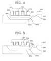
- FIG. 4is a cross-sectional view illustrating a capacitor according to a second embodiment of the present invention.
- the capacitor according to the second embodiment of the present inventionhas the same constituent elements as in the first embodiment, except for which a middle electrode 405 and a top electrode 407 have different shapes from the middle electrode 205 and the top electrode 207 of the capacitor according to the first embodiment of the present invention. Accordingly, the elements which are the same as those in FIG. 2 will have the same reference numbers.
- the middle electrode 405has patterns of which a plurality of stakes are put up.
- the dielectric film 206is formed on surfaces of each of the middle electrodes 405 and the top electrode 407 of the capacitor is formed over the overall surface of the dielectric film.
- the top electrode 407 which is filled in the patterns of the middle electrode 405has a comb shape. According to the second embodiment of the present invention, since the surface area where the middle electrode faces the top electrode is increased compared to the first embodiment, the capacitance thereof is accordingly greater than that of the capacitor according to the first embodiment of the present invention.
- FIG. 5is a cross-sectional view illustrating a capacitor according to a third embodiment of the present invention.
- the capacitor according to the third embodiment of the present inventionhas the same constituent elements as in the second embodiment, except for which a middle electrode 505 has a different shape from the middle electrode 405 of the capacitor according to the second embodiment of the present invention. Accordingly, the elements which are the same as those in FIG. 3 will have the same reference numbers.
- the middle electrode 505is formed in a comb shape.
- a dielectric film 206is formed over the middle electrode 505 .
- the middle electrode 505 and the top electrode 507have the shape of which teeth of two combs bite facing each other.
- the capacitor according to the third embodiment of the present inventionadvantageously has greater capacitance than that of the first embodiment of the present invention.
- the capacitor according to the present inventionvariously changes the shape of the middle electrode or the top electrode to enlarge the surface area thereof and thereby increases the capacitance.
- the fabrication method of the capacitor according to the second embodiment of the present inventionadopts steps which are the same as the steps shown in FIG. 3 A through FIG. 3H employed in the first embodiment of the present invention.
- the second polysilicon layer 310 in FIG. 3His patterned to form second polysilicon layer patterns 310 b , 310 c , the second polysilicon patterns 310 c having patterns of a plurality of stakes which are separately put up on the second insulating film 307 a (that is, the first dielectric film) or island shapes.
- a third polysilicon layer and a fourth insulating filmare formed on the overall surface of the resultant structure of FIG.
- the bottom electrodeis buried in the trench, the height of the capacitor is controlled, which results in reduction of the step difference of the elements formed on the active and isolation regions of the semiconductor substrate. Also, when the same voltage is applied to the bottom and top electrodes, the overall capacitance becomes a value that the capacitance between the bottom and middle electrodes is added to the capacitance between the middle and top electrodes, thus having an effect of increasing the capacitance compared to the conventional art while occupying the the same area on the semiconductor substrate as in the conventional art.
- the capacitor according to the present inventionhas an effect of varying the capacitance in accordance with the combination of the applied voltage with the same electrode structure.
- the capacitor according to the second and third embodiments of the present inventionhas an advantage of increasing the capacitance compared to the first embodiment, as well as having the same effects as the capacitor in the first embodiment, by forming the middle electrode in the stake or comb shape, thereby enlarging the surface area at its maximum.
- a hemispheric conductive film or a plurality of dimplescan be formed on the middle electrode of the capacitor according to one of the above embodiments of the present invention, thereby increasing the surface area of the middle electrode and eventually fabricating a capacitor having high capacitance.
Landscapes
- Semiconductor Integrated Circuits (AREA)
Abstract
Description
Claims (20)
Applications Claiming Priority (2)
| Application Number | Priority Date | Filing Date | Title |
|---|---|---|---|
| KR99-14026 | 1999-04-20 | ||
| KR1019990014026AKR100319618B1 (en) | 1999-04-20 | 1999-04-20 | Capacitor for semiconductor device fabricating method thereof |
Publications (1)
| Publication Number | Publication Date |
|---|---|
| US6373083B1true US6373083B1 (en) | 2002-04-16 |
Family
ID=19581088
Family Applications (1)
| Application Number | Title | Priority Date | Filing Date |
|---|---|---|---|
| US09/392,632Expired - LifetimeUS6373083B1 (en) | 1999-04-20 | 1999-09-09 | Capacitor for semiconductor device and fabrication method thereof |
Country Status (2)
| Country | Link |
|---|---|
| US (1) | US6373083B1 (en) |
| KR (1) | KR100319618B1 (en) |
Cited By (7)
| Publication number | Priority date | Publication date | Assignee | Title |
|---|---|---|---|---|
| US20020090777A1 (en)* | 2001-01-05 | 2002-07-11 | Leonard Forbes | Methods of forming capacitor structures, and capacitor structures |
| US6627936B2 (en)* | 2001-06-07 | 2003-09-30 | Umc Japan | Semiconductor device and method of producing the same |
| US20030183884A1 (en)* | 2002-03-28 | 2003-10-02 | Fujitsu Quantum Devices Limited | Interdigital capacitor and method for adjusting the same |
| US6664580B2 (en)* | 2001-07-16 | 2003-12-16 | Taiwan Semiconductor Manufacturing Company | Buried PIP capacitor for mixed-mode process |
| EP1420442A2 (en) | 2002-11-15 | 2004-05-19 | STMicroelectronics S.r.l. | Process for self-aligned manufacture of integrated electronic devices |
| US20050139887A1 (en)* | 2003-12-31 | 2005-06-30 | Dongbuanam Semiconductor Inc. | Methods of fabricating capacitor |
| US7022565B1 (en)* | 2004-11-26 | 2006-04-04 | Grace Semiconductor Manufacturing Corporation | Method of fabricating a trench capacitor of a mixed mode integrated circuit |
Citations (3)
| Publication number | Priority date | Publication date | Assignee | Title |
|---|---|---|---|---|
| US5770876A (en)* | 1995-04-13 | 1998-06-23 | International Business Machines Corporation | Semiconductor trench capacitor cell having a buried strap |
| US5959326A (en)* | 1996-05-08 | 1999-09-28 | Nec Corporation | Capacitor incorporated in semiconductor device having a lower electrode composed of multi-layers or of graded impurity concentration |
| US6015729A (en)* | 1995-10-06 | 2000-01-18 | Micron Technology, Inc. | Integrated chip multilayer decoupling capcitors |
Family Cites Families (4)
| Publication number | Priority date | Publication date | Assignee | Title |
|---|---|---|---|---|
| JPS6070754A (en)* | 1983-09-27 | 1985-04-22 | Omron Tateisi Electronics Co | Manufacture of hybrid integrated circuit |
| KR920015550A (en)* | 1991-01-23 | 1992-08-27 | 김광호 | Method of manufacturing a capacitor |
| JPH0582761A (en)* | 1991-09-19 | 1993-04-02 | Olympus Optical Co Ltd | Ferroelectric substance memory |
| JPH07111313A (en)* | 1993-10-12 | 1995-04-25 | Rohm Co Ltd | Semiconductor capacitive element |
- 1999
- 1999-04-20KRKR1019990014026Apatent/KR100319618B1/ennot_activeExpired - Fee Related
- 1999-09-09USUS09/392,632patent/US6373083B1/ennot_activeExpired - Lifetime
Patent Citations (3)
| Publication number | Priority date | Publication date | Assignee | Title |
|---|---|---|---|---|
| US5770876A (en)* | 1995-04-13 | 1998-06-23 | International Business Machines Corporation | Semiconductor trench capacitor cell having a buried strap |
| US6015729A (en)* | 1995-10-06 | 2000-01-18 | Micron Technology, Inc. | Integrated chip multilayer decoupling capcitors |
| US5959326A (en)* | 1996-05-08 | 1999-09-28 | Nec Corporation | Capacitor incorporated in semiconductor device having a lower electrode composed of multi-layers or of graded impurity concentration |
Cited By (21)
| Publication number | Priority date | Publication date | Assignee | Title |
|---|---|---|---|---|
| US20050026355A1 (en)* | 2001-01-05 | 2005-02-03 | Leonard Forbes | Capacitor structures |
| US20020164852A1 (en)* | 2001-01-05 | 2002-11-07 | Leonard Forbes | Capacitor structures |
| US7192827B2 (en) | 2001-01-05 | 2007-03-20 | Micron Technology, Inc. | Methods of forming capacitor structures |
| US7166883B2 (en)* | 2001-01-05 | 2007-01-23 | Micron Technology, Inc. | Capacitor structures |
| US20050167723A1 (en)* | 2001-01-05 | 2005-08-04 | Leonard Forbes | Capacitor structures |
| US20020090777A1 (en)* | 2001-01-05 | 2002-07-11 | Leonard Forbes | Methods of forming capacitor structures, and capacitor structures |
| US6627936B2 (en)* | 2001-06-07 | 2003-09-30 | Umc Japan | Semiconductor device and method of producing the same |
| US6664580B2 (en)* | 2001-07-16 | 2003-12-16 | Taiwan Semiconductor Manufacturing Company | Buried PIP capacitor for mixed-mode process |
| US6903402B2 (en)* | 2002-03-28 | 2005-06-07 | Fujitsu Quantum Devices, Ltd. | Interdigital capacitor having a cutting target portion |
| US20050064657A1 (en)* | 2002-03-28 | 2005-03-24 | Naoyuki Miyazawa | Interdigital capacitor and method for adjusting the same |
| US7015109B2 (en) | 2002-03-28 | 2006-03-21 | Fujitsu Quantum Devices Limited | Interdigital capacitor and method for adjusting the same |
| US20030183884A1 (en)* | 2002-03-28 | 2003-10-02 | Fujitsu Quantum Devices Limited | Interdigital capacitor and method for adjusting the same |
| EP1420442A3 (en)* | 2002-11-15 | 2004-12-22 | STMicroelectronics S.r.l. | Process for self-aligned manufacture of integrated electronic devices |
| US20040173869A1 (en)* | 2002-11-15 | 2004-09-09 | Stmicroelectronics S.R.L. | Process for self-aligned manufacture of integrated electronic devices |
| EP1420442A2 (en) | 2002-11-15 | 2004-05-19 | STMicroelectronics S.r.l. | Process for self-aligned manufacture of integrated electronic devices |
| US20080108200A1 (en)* | 2002-11-15 | 2008-05-08 | Stmicroelectronics S.R.L. | Process for self-aligned manufacture of integrated electronic devices |
| US7468535B2 (en) | 2002-11-15 | 2008-12-23 | Roberto Bez | Self-aligned integrated electronic devices |
| US7772084B2 (en) | 2002-11-15 | 2010-08-10 | Roberto Bez | Process for self-aligned manufacture of integrated electronic devices |
| US20050139887A1 (en)* | 2003-12-31 | 2005-06-30 | Dongbuanam Semiconductor Inc. | Methods of fabricating capacitor |
| US7605418B2 (en) | 2003-12-31 | 2009-10-20 | Dongbu Electronics Co., Ltd. | Methods of fabricating capacitor |
| US7022565B1 (en)* | 2004-11-26 | 2006-04-04 | Grace Semiconductor Manufacturing Corporation | Method of fabricating a trench capacitor of a mixed mode integrated circuit |
Also Published As
| Publication number | Publication date |
|---|---|
| KR100319618B1 (en) | 2002-01-05 |
| KR20000066725A (en) | 2000-11-15 |
Similar Documents
| Publication | Publication Date | Title |
|---|---|---|
| US9431476B2 (en) | Semiconductor devices including capacitors and methods of manufacturing the same | |
| JP2994239B2 (en) | SOI trench structure and method of manufacturing the same | |
| JP4167727B2 (en) | Semiconductor memory device | |
| US5804852A (en) | Stacked capacitor DRAM structure featuring a multiple crown shaped polysilicon lower electrode | |
| JPH0653412A (en) | Semiconductor memory device and fabrication thereof | |
| JPH0226065A (en) | Stacked capacitor DRAM cell and its manufacturing method | |
| US6656814B2 (en) | Methods of fabricating integrated circuit devices including distributed and isolated dummy conductive regions | |
| US20030008453A1 (en) | Semiconductor device having a contact window and fabrication method thereof | |
| KR100456577B1 (en) | Capacitor Of Semiconductor Device And Method Of Fabricating The Same | |
| TW200901378A (en) | Recess channel MOS transistor device and fabricating method thereof | |
| US6373083B1 (en) | Capacitor for semiconductor device and fabrication method thereof | |
| JP3321788B2 (en) | MIS type semiconductor device and method of manufacturing the same | |
| US6093622A (en) | Isolation method of semiconductor device using second pad oxide layer formed through chemical vapor deposition (CVD) | |
| US5989954A (en) | Method for forming a cylinder capacitor in the dram process | |
| US6987044B2 (en) | Volatile memory structure and method for forming the same | |
| KR100449251B1 (en) | Method for forming of semiconductor device | |
| JP2002009183A (en) | Semiconductor memory device and method of manufacturing the same | |
| JPH05226583A (en) | Semiconductor device and manufacture thereof | |
| JPH04107858A (en) | Dynamic type semiconductor memory and manufacturing method thereof | |
| KR100445059B1 (en) | Method of fabricating capacitor of semiconductor device for improving physical property of capacitor bottom electrode | |
| TWI248158B (en) | Structure and manufacturing method of composite single sided buried strap | |
| KR960013639B1 (en) | Manufacture and structure of semiconductor memory cell | |
| KR20040009383A (en) | Semiconductor memory device having stacked capacitor and trench capacitor, and method for fabricating the same | |
| JPH07111312A (en) | Semiconductor capacitive element | |
| KR100200747B1 (en) | Device isolation method of semiconductor device |
Legal Events
| Date | Code | Title | Description |
|---|---|---|---|
| AS | Assignment | Owner name:HYUNDAI MICRO ELECTRONICS CO., LTD., KOREA, REPUBL Free format text:ASSIGNMENT OF ASSIGNORS INTEREST;ASSIGNOR:OH, BO-SEOK;REEL/FRAME:010237/0423 Effective date:19990810 | |
| AS | Assignment | Owner name:HYUNDAI ELECTRONICS INDUSTRIES, CO., LTD., KOREA, Free format text:MERGER;ASSIGNOR:LG SEMICON CO., LTD.;REEL/FRAME:010951/0606 Effective date:19991020 | |
| STCF | Information on status: patent grant | Free format text:PATENTED CASE | |
| AS | Assignment | Owner name:HYNIX SEMICONDUCTOR INC., KOREA, REPUBLIC OF Free format text:CHANGE OF NAME;ASSIGNOR:HYUNDAI ELECTRONICS INDUSTRIES CO., LTD.;REEL/FRAME:015242/0899 Effective date:20010329 | |
| AS | Assignment | Owner name:MAGNACHIP SEMICONDUCTOR, LTD., KOREA, REPUBLIC OF Free format text:ASSIGNMENT OF ASSIGNORS INTEREST;ASSIGNOR:HYNIX SEMICONDUCTOR, INC.;REEL/FRAME:016216/0649 Effective date:20041004 | |
| FPAY | Fee payment | Year of fee payment:4 | |
| AS | Assignment | Owner name:U.S. BANK NATIONAL ASSOCIATION, AS COLLATERAL TRUS Free format text:AFTER-ACQUIRED INTELLECTUAL PROPERTY KUN-PLEDGE AGREEMENT;ASSIGNOR:MAGNACHIP SEMICONDUCTOR, LTD.;REEL/FRAME:022277/0133 Effective date:20090217 | |
| FPAY | Fee payment | Year of fee payment:8 | |
| FEPP | Fee payment procedure | Free format text:PAYOR NUMBER ASSIGNED (ORIGINAL EVENT CODE: ASPN); ENTITY STATUS OF PATENT OWNER: LARGE ENTITY | |
| AS | Assignment | Owner name:MAGNACHIP SEMICONDUCTOR LTD.,KOREA, DEMOCRATIC PEO Free format text:RELEASE BY SECURED PARTY;ASSIGNOR:U.S. BANK NATIONAL ASSOCIATION;REEL/FRAME:024563/0807 Effective date:20100527 | |
| FPAY | Fee payment | Year of fee payment:12 | |
| AS | Assignment | Owner name:MAGNACHIP SEMICONDUCTOR LTD., KOREA, REPUBLIC OF Free format text:CORRECTIVE ASSIGNMENT TO CORRECT THE RECEIVING PARTY ADDRESS PREVIOUSLY RECORDED AT REEL: 024563 FRAME: 0807. ASSIGNOR(S) HEREBY CONFIRMS THE RELEASE BY SECURED PARTY;ASSIGNOR:US BANK NATIONAL ASSOCIATION;REEL/FRAME:034469/0001 Effective date:20100527 |