US6372657B1 - Method for selective etching of oxides - Google Patents
Method for selective etching of oxidesDownload PDFInfo
- Publication number
- US6372657B1 US6372657B1US09/653,554US65355400AUS6372657B1US 6372657 B1US6372657 B1US 6372657B1US 65355400 AUS65355400 AUS 65355400AUS 6372657 B1US6372657 B1US 6372657B1
- Authority
- US
- United States
- Prior art keywords
- flow rate
- plasma
- sccm
- gaseous mixture
- source chamber
- Prior art date
- Legal status (The legal status is an assumption and is not a legal conclusion. Google has not performed a legal analysis and makes no representation as to the accuracy of the status listed.)
- Expired - Lifetime, expires
Links
- 238000000034methodMethods0.000titleclaimsabstractdescription67
- 238000005530etchingMethods0.000titleclaimsdescription44
- 239000000758substrateSubstances0.000claimsabstractdescription59
- 239000004065semiconductorSubstances0.000claimsabstractdescription27
- 238000004140cleaningMethods0.000claimsabstractdescription20
- 238000011144upstream manufacturingMethods0.000claimsabstractdescription11
- 239000008246gaseous mixtureSubstances0.000claimsdescription39
- 238000001020plasma etchingMethods0.000claimsdescription10
- QGZKDVFQNNGYKY-UHFFFAOYSA-NAmmoniaChemical compoundNQGZKDVFQNNGYKY-UHFFFAOYSA-N0.000abstractdescription58
- 229910000069nitrogen hydrideInorganic materials0.000abstractdescription41
- 230000008569processEffects0.000abstractdescription26
- 238000006243chemical reactionMethods0.000abstractdescription9
- 229910021529ammoniaInorganic materials0.000abstractdescription8
- QVGXLLKOCUKJST-UHFFFAOYSA-Natomic oxygenChemical compound[O]QVGXLLKOCUKJST-UHFFFAOYSA-N0.000abstractdescription8
- QKCGXXHCELUCKW-UHFFFAOYSA-Nn-[4-[4-(dinaphthalen-2-ylamino)phenyl]phenyl]-n-naphthalen-2-ylnaphthalen-2-amineChemical compoundC1=CC=CC2=CC(N(C=3C=CC(=CC=3)C=3C=CC(=CC=3)N(C=3C=C4C=CC=CC4=CC=3)C=3C=C4C=CC=CC4=CC=3)C3=CC4=CC=CC=C4C=C3)=CC=C21QKCGXXHCELUCKW-UHFFFAOYSA-N0.000abstractdescription8
- 239000001301oxygenSubstances0.000abstractdescription7
- 229910052760oxygenInorganic materials0.000abstractdescription7
- 239000000203mixtureSubstances0.000abstractdescription5
- GVGCUCJTUSOZKP-UHFFFAOYSA-Nnitrogen trifluorideChemical compoundFN(F)FGVGCUCJTUSOZKP-UHFFFAOYSA-N0.000description41
- VYPSYNLAJGMNEJ-UHFFFAOYSA-NSilicium dioxideChemical compoundO=[Si]=OVYPSYNLAJGMNEJ-UHFFFAOYSA-N0.000description35
- 239000007789gasSubstances0.000description24
- 229910052814silicon oxideInorganic materials0.000description21
- XUIMIQQOPSSXEZ-UHFFFAOYSA-NSiliconChemical compound[Si]XUIMIQQOPSSXEZ-UHFFFAOYSA-N0.000description16
- 230000008859changeEffects0.000description16
- 229910052710siliconInorganic materials0.000description16
- 239000010703siliconSubstances0.000description16
- 238000002474experimental methodMethods0.000description13
- 238000011282treatmentMethods0.000description12
- 235000012239silicon dioxideNutrition0.000description7
- KRHYYFGTRYWZRS-UHFFFAOYSA-NFluoraneChemical compoundFKRHYYFGTRYWZRS-UHFFFAOYSA-N0.000description6
- 239000000377silicon dioxideSubstances0.000description6
- 230000004927fusionEffects0.000description4
- 238000005259measurementMethods0.000description4
- QPJSUIGXIBEQAC-UHFFFAOYSA-Nn-(2,4-dichloro-5-propan-2-yloxyphenyl)acetamideChemical compoundCC(C)OC1=CC(NC(C)=O)=C(Cl)C=C1ClQPJSUIGXIBEQAC-UHFFFAOYSA-N0.000description4
- 230000015572biosynthetic processEffects0.000description3
- 239000004020conductorSubstances0.000description3
- 150000002500ionsChemical class0.000description3
- 239000005360phosphosilicate glassSubstances0.000description3
- 239000000126substanceSubstances0.000description3
- ZOXJGFHDIHLPTG-UHFFFAOYSA-NBoronChemical compound[B]ZOXJGFHDIHLPTG-UHFFFAOYSA-N0.000description2
- OAICVXFJPJFONN-UHFFFAOYSA-NPhosphorusChemical compound[P]OAICVXFJPJFONN-UHFFFAOYSA-N0.000description2
- BOTDANWDWHJENH-UHFFFAOYSA-NTetraethyl orthosilicateChemical compoundCCO[Si](OCC)(OCC)OCCBOTDANWDWHJENH-UHFFFAOYSA-N0.000description2
- 230000004888barrier functionEffects0.000description2
- 229910052796boronInorganic materials0.000description2
- 238000011143downstream manufacturingMethods0.000description2
- 238000005108dry cleaningMethods0.000description2
- 239000012212insulatorSubstances0.000description2
- 229910052751metalInorganic materials0.000description2
- 239000002184metalSubstances0.000description2
- 229910052698phosphorusInorganic materials0.000description2
- 239000011574phosphorusSubstances0.000description2
- 239000010936titaniumSubstances0.000description2
- 238000001039wet etchingMethods0.000description2
- JBRZTFJDHDCESZ-UHFFFAOYSA-NAsGaChemical compound[As]#[Ga]JBRZTFJDHDCESZ-UHFFFAOYSA-N0.000description1
- 229910001218Gallium arsenideInorganic materials0.000description1
- UFHFLCQGNIYNRP-UHFFFAOYSA-NHydrogenChemical compound[H][H]UFHFLCQGNIYNRP-UHFFFAOYSA-N0.000description1
- BLRPTPMANUNPDV-UHFFFAOYSA-NSilaneChemical compound[SiH4]BLRPTPMANUNPDV-UHFFFAOYSA-N0.000description1
- 229910000577Silicon-germaniumInorganic materials0.000description1
- RTAQQCXQSZGOHL-UHFFFAOYSA-NTitaniumChemical compound[Ti]RTAQQCXQSZGOHL-UHFFFAOYSA-N0.000description1
- LEVVHYCKPQWKOP-UHFFFAOYSA-N[Si].[Ge]Chemical compound[Si].[Ge]LEVVHYCKPQWKOP-UHFFFAOYSA-N0.000description1
- 238000001816coolingMethods0.000description1
- 238000007598dipping methodMethods0.000description1
- 238000006073displacement reactionMethods0.000description1
- 238000001312dry etchingMethods0.000description1
- 230000000694effectsEffects0.000description1
- MUJOIMFVNIBMKC-UHFFFAOYSA-NfludioxonilChemical compoundC=12OC(F)(F)OC2=CC=CC=1C1=CNC=C1C#NMUJOIMFVNIBMKC-UHFFFAOYSA-N0.000description1
- 229910052732germaniumInorganic materials0.000description1
- GNPVGFCGXDBREM-UHFFFAOYSA-Ngermanium atomChemical compound[Ge]GNPVGFCGXDBREM-UHFFFAOYSA-N0.000description1
- 238000010438heat treatmentMethods0.000description1
- 239000001257hydrogenSubstances0.000description1
- 229910052739hydrogenInorganic materials0.000description1
- 239000011810insulating materialSubstances0.000description1
- 238000010884ion-beam techniqueMethods0.000description1
- 238000012986modificationMethods0.000description1
- 230000004048modificationEffects0.000description1
- 239000003921oilSubstances0.000description1
- 230000003647oxidationEffects0.000description1
- 238000007254oxidation reactionMethods0.000description1
- 238000002161passivationMethods0.000description1
- 230000035515penetrationEffects0.000description1
- 238000000206photolithographyMethods0.000description1
- 229920002120photoresistant polymerPolymers0.000description1
- 238000000623plasma-assisted chemical vapour depositionMethods0.000description1
- 238000012545processingMethods0.000description1
- 239000010453quartzSubstances0.000description1
- 238000010405reoxidation reactionMethods0.000description1
- 229910052594sapphireInorganic materials0.000description1
- 239000010980sapphireSubstances0.000description1
- 229910000077silaneInorganic materials0.000description1
- 238000006467substitution reactionMethods0.000description1
- 229910052719titaniumInorganic materials0.000description1
- WFKWXMTUELFFGS-UHFFFAOYSA-NtungstenChemical compound[W]WFKWXMTUELFFGS-UHFFFAOYSA-N0.000description1
- 229910052721tungstenInorganic materials0.000description1
- 239000010937tungstenSubstances0.000description1
- XLYOFNOQVPJJNP-UHFFFAOYSA-NwaterSubstancesOXLYOFNOQVPJJNP-UHFFFAOYSA-N0.000description1
- 238000009736wettingMethods0.000description1
Images


Classifications
- H—ELECTRICITY
- H01—ELECTRIC ELEMENTS
- H01L—SEMICONDUCTOR DEVICES NOT COVERED BY CLASS H10
- H01L21/00—Processes or apparatus adapted for the manufacture or treatment of semiconductor or solid state devices or of parts thereof
- H01L21/02—Manufacture or treatment of semiconductor devices or of parts thereof
- H01L21/04—Manufacture or treatment of semiconductor devices or of parts thereof the devices having potential barriers, e.g. a PN junction, depletion layer or carrier concentration layer
- H01L21/18—Manufacture or treatment of semiconductor devices or of parts thereof the devices having potential barriers, e.g. a PN junction, depletion layer or carrier concentration layer the devices having semiconductor bodies comprising elements of Group IV of the Periodic Table or AIIIBV compounds with or without impurities, e.g. doping materials
- H01L21/30—Treatment of semiconductor bodies using processes or apparatus not provided for in groups H01L21/20 - H01L21/26
- H01L21/302—Treatment of semiconductor bodies using processes or apparatus not provided for in groups H01L21/20 - H01L21/26 to change their surface-physical characteristics or shape, e.g. etching, polishing, cutting
- H01L21/306—Chemical or electrical treatment, e.g. electrolytic etching
- H01L21/3065—Plasma etching; Reactive-ion etching
- H—ELECTRICITY
- H01—ELECTRIC ELEMENTS
- H01L—SEMICONDUCTOR DEVICES NOT COVERED BY CLASS H10
- H01L21/00—Processes or apparatus adapted for the manufacture or treatment of semiconductor or solid state devices or of parts thereof
- H01L21/02—Manufacture or treatment of semiconductor devices or of parts thereof
- H01L21/02041—Cleaning
- H01L21/02043—Cleaning before device manufacture, i.e. Begin-Of-Line process
- H01L21/02046—Dry cleaning only
- H—ELECTRICITY
- H01—ELECTRIC ELEMENTS
- H01L—SEMICONDUCTOR DEVICES NOT COVERED BY CLASS H10
- H01L21/00—Processes or apparatus adapted for the manufacture or treatment of semiconductor or solid state devices or of parts thereof
- H01L21/02—Manufacture or treatment of semiconductor devices or of parts thereof
- H01L21/02041—Cleaning
- H01L21/02057—Cleaning during device manufacture
- H01L21/0206—Cleaning during device manufacture during, before or after processing of insulating layers
- H01L21/02063—Cleaning during device manufacture during, before or after processing of insulating layers the processing being the formation of vias or contact holes
- H—ELECTRICITY
- H01—ELECTRIC ELEMENTS
- H01L—SEMICONDUCTOR DEVICES NOT COVERED BY CLASS H10
- H01L21/00—Processes or apparatus adapted for the manufacture or treatment of semiconductor or solid state devices or of parts thereof
- H01L21/02—Manufacture or treatment of semiconductor devices or of parts thereof
- H01L21/04—Manufacture or treatment of semiconductor devices or of parts thereof the devices having potential barriers, e.g. a PN junction, depletion layer or carrier concentration layer
- H01L21/18—Manufacture or treatment of semiconductor devices or of parts thereof the devices having potential barriers, e.g. a PN junction, depletion layer or carrier concentration layer the devices having semiconductor bodies comprising elements of Group IV of the Periodic Table or AIIIBV compounds with or without impurities, e.g. doping materials
- H01L21/30—Treatment of semiconductor bodies using processes or apparatus not provided for in groups H01L21/20 - H01L21/26
- H01L21/31—Treatment of semiconductor bodies using processes or apparatus not provided for in groups H01L21/20 - H01L21/26 to form insulating layers thereon, e.g. for masking or by using photolithographic techniques; After treatment of these layers; Selection of materials for these layers
- H01L21/3105—After-treatment
- H01L21/311—Etching the insulating layers by chemical or physical means
- H01L21/31105—Etching inorganic layers
- H01L21/31111—Etching inorganic layers by chemical means
- H01L21/31116—Etching inorganic layers by chemical means by dry-etching
- H—ELECTRICITY
- H01—ELECTRIC ELEMENTS
- H01L—SEMICONDUCTOR DEVICES NOT COVERED BY CLASS H10
- H01L21/00—Processes or apparatus adapted for the manufacture or treatment of semiconductor or solid state devices or of parts thereof
- H01L21/70—Manufacture or treatment of devices consisting of a plurality of solid state components formed in or on a common substrate or of parts thereof; Manufacture of integrated circuit devices or of parts thereof
- H01L21/71—Manufacture of specific parts of devices defined in group H01L21/70
- H01L21/768—Applying interconnections to be used for carrying current between separate components within a device comprising conductors and dielectrics
- H01L21/76801—Applying interconnections to be used for carrying current between separate components within a device comprising conductors and dielectrics characterised by the formation and the after-treatment of the dielectrics, e.g. smoothing
- H01L21/76802—Applying interconnections to be used for carrying current between separate components within a device comprising conductors and dielectrics characterised by the formation and the after-treatment of the dielectrics, e.g. smoothing by forming openings in dielectrics
- H01L21/76814—Applying interconnections to be used for carrying current between separate components within a device comprising conductors and dielectrics characterised by the formation and the after-treatment of the dielectrics, e.g. smoothing by forming openings in dielectrics post-treatment or after-treatment, e.g. cleaning or removal of oxides on underlying conductors
Definitions
- the present inventionrelates to the field of semiconductor integrated circuits and, in particular, to a method for selectively etching of oxides.
- a native oxide residuefor example silicon dioxide, often remains, particularly at the bottom of the opening.
- This native oxide residuemust be removed before a conductor is deposited in the opening, as the oxide residue will undesirably increase resistance and inhibit current flow through the conductor.
- the semiconductor surfacemust also be passivated by hydrogen to further prevent its reoxidation after the removal of the native oxide.
- BOEbuffered oxide etch
- HFhydrofluoric acid
- silicon dioxide grown in dry oxygenhas a slower etch rate than that of the silicon oxide grown in the presence of water. Further, a high concentration of phosphorus in the oxide enhances the etch rate, whereas a high boron concentration reduces the oxide etch rate.
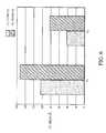
- FIG. 1illustrates a contact opening 22 formed according to well-known photolithography processes in an insulating layer 24 of, for example, BPSG that has been applied over a semiconductor substrate 20 .
- a bit line conductor(not shown) of for example tungsten (W) will be later formed, as known in the art.
- a barrier layer(not shown), formed of a metal such as titanium (Ti) is first applied on surface 21 of tie contact opening 22 prior to the formation of the bit line connector. Since, as explained above, a native oxide 23 (FIG.
- FIG. 1shows how removal of the native oxide 23 increases the diameter D of the contact opening 22 .
- This changeis illustrated by the change in critical dimension CD, that is, ⁇ CD 25 formed as a result of the wet cleaning processes of the prior art.
- FIG. 3exemplifies the time dependency of the change in the critical dimension ( ⁇ CD) for the contact opening 22 of FIG. 1, which undergoes a modified BOE wet etching treatment used in the prior art.
- the BOE treatmentgives an increase in CD because it etches the adjacent insulating layer 24 (FIG. 1 ).
- the change in the critical dimension ⁇ CD 1is high, of about 180 Angstroms.
- This increase in the diameter of the contact opening 22also impacts the displacement of the metal atoms that fill the contact opening.
- electrical contactsmay also become unreliable.
- the present inventionprovides a dry plasma cleaning process for the removal of native oxides, or other oxide films or growth residue, formed on a semiconductor substrate, without damaging the substrate or affecting the critical dimension of a pattern on such substrate and with less damage to a downstream processing chamber.
- the inventionis particularly useful for the selective etching of silicon dioxide residue at the bottom of a contact opening which is formed in a BPSG doped insulating layer.
- the inventionis also useful for the etching of undoped oxides, such as thermally grown SiO 2 , at a faster rate than that for doped oxides, such as BPSG.
- the present inventionuses a gaseous mixture of nitrogen trifluoride (NF 3 ) and ammonia (NH 3 ), which is first injected upstream into a microwave plasma source which excites them, and then both gases flow downstream in plasma form onto a substrate surface.
- NF 3nitrogen trifluoride
- NH 3ammonia
- the method of the present inventionprovides a dry cleaning process for damageless removal of native oxides and/or growth residue from the bottom of a contact opening, without significantly affecting the critical dimension of such contact opening and with less damage to a downstream processing chamber.
- the inventionalso provides a dry plasma technique for etching undoped oxides faster than doped oxides.
- FIG. 1is a schematic cross-sectional view of a portion of a representative semiconductor substrate with a conventional contact opening formed in an insulating layer accordance with the prior art.
- FIG. 2depicts the loss in critical dimension of the contact opening of FIG. 1 when it undergoes a wet cleaning treatment in accordance with the prior art.
- FIG. 3is a graph illustrating the time dependency of changes in the critical dimension of the contact opening of FIG. 1 when it undergoes an etching treatment in accordance with the prior art.
- FIG. 4is a schematic view of the fusion plasma reactor apparatus used in the present invention.
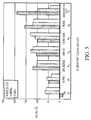
- FIG. 5shows the etching depths for thermally grown SiO 2 and BPSG insulators and the change in the critical dimension of a contact opening which undergo different etching treatments according to a method of the present invention.
- FIG. 6shows a comparison of the change in critical dimension of a contact opening formed using etching treatments according to a method of the prior art and according to a method of the present invention.
- substrateused in the following description may include any semiconductor-based structure. Structure must be understood to include silicon, silicon-on insulator (SOI), silicon-on sapphire (SOS), doped and undoped semiconductors, epitaxial layers of silicon supported by a base semiconductor foundation, and other semiconductor structures.
- SOIsilicon-on insulator
- SOSsilicon-on sapphire
- the semiconductorneed not be silicon-based.
- the semiconductorcould be silicon-germanium, germanium, or gallium arsenide.
- partis used to indicate one of several equal units of which the gaseous mixtures used in the present invention are comprised. Because all gases are used at identical pressures and temperatures, the term part is used instead of other terminology (for example, moles) to underscore the importance of using gases mi particular ratios as opposed to in particular amounts.
- the present inventionprovides a plasma etching and cleaning process for the removal of native oxides, or other oxide films or growth residue, formed over a substrate, without damaging the substrate or affecting the critical dimension of a pattern formed over such substrate.
- the inventionalso provides a method for achieving a faster etching rate for undoped oxides, as opposed to doped oxides.
- the inventionis particularly useful in removing native oxides from the bottom of contact openings etched in an insulating layer formed over a substrate.
- the present inventionuses a mixture of nitrogen trifluoride (NF 3 ) and ammonia (NH 3 ) gases, which is injected upstream into a microwave plasma source which excites them, and then the upstream plasma flows downstream in a plasma form onto the substrate surface.
- NF 3nitrogen trifluoride
- NH 3ammonia
- FIG. 4shows a schematic view of apparatus 100 employed in die present invention.
- a plasma source chamber 12is remotely positioned from a reaction chamber 14 .
- the plasma source chamber 12excites a gaseous mixture 10 into a plasma prior to the transport of the gaseous mixture to the reaction chamber 14 , through a conduit 30 (FIG. 4 ).
- FIG. 4also shows a substrate 32 located on a substrate stage or table 34 , which supports the substrate 32 through a chuck 38 , which mechanically or electrostatically holds the substrate 32 to table 34 .
- the substrate table 34is also provided with a cooling device 36 which cools the substrate table 34 .
- a heating lamp 42 located on die outside of the reaction chamber 14maintains die temperature of the substrate 32 constant and also helps reduce the amount of residue that is eventually formed on the walls of die reaction chamber 14 .
- the plasma apparatus 100is also provided with a microwave cavity 16 , which is connected to the plasma source chamber 12 through a wave inlet 17 .
- Microwaves at, for example, 2.45 GHzare generated in the cavity 16 and applied through the wave inlet 17 to the plasma source chamber 12 .
- gas inlets 12 a , 12 b , and 12 care gas inlets 12 a , 12 b , and 12 c , through which suitable etching gases may be introduced in the source chamber 12 in accordance with the present invention.
- the microwave cavity 16 , the wave inlet 17 , die reaction chamber 14 , the plasma source chamber 12 , and the conduit 30are formed of quartz or, more preferably, of saphire.
- a selective etching and cleaning method for native oxides, such as SiO 2 , from the bottoms of contact openings etched into a BPSG insulating layeris explained below using the apparatus 100 of FIG. 4 .
- the apparatus 100 of FIG. 4may be also used, in general, for etclhing undoped oxides faster than doped oxides.
- the etching process of the present inventionis carried out in the reaction chamber 14 , which is a high density plasma (HDP) etcher.
- HDPhigh density plasma
- a cleaning etchis a reactive ion etch, which is a combination of chemical plasma etching, in which a plasma etches by chemically reacting with the substrate, and ion beam etching, which is a physical process using high energy ions to bombard die substrate in order to etch it.
- the fusion plasma of the present inventionused for selectively etching and cleaning of native oxides, includes a gaseous mixture 10 of nitrogen trifluoride (NF 3 ) and ammonia (NH 3 ). Both gases are first injected through their respective gas inlets 12 a , 12 b (FIG. 4) into the plasma source chamber 12 .
- a microwavetypically of 2.45 GHz at 500 W, housed within the microwave cavity 16 , is excited and the resulting microwave is applied through the wave inlet 17 to tie plasma source chamber 12 containing the NH 3 /NF 3 gaseous mixture 10 .
- a dischargeis generated inside die plasma source chamber 12 and die gases forming the NH 3 /NF 3 gaseous mixture 10 are decomposed.
- both NF 3 and NH 3 gasesare first injected upstream, and only then do both flow downstream as a plasma from tie plasma source chamber 12 , to the reaction chamber 14 onto the surface of the substrate 32 .
- the plasma etching process of the present inventionuses the two etching gases ammonia (NH 3 ) and nitrogen trifluoride (NF 3 ) injected into the plasma source chamber 12 at a rate of approximately 1000-4000 standard cubic centimeters per minute (sccm) for NH 3 , and a rate of approximately 25-200 standard cubic centimeters per minute (sccm) for NF 3 .
- Oxygen (O 2 )may also be injected with the NH 3 /NF 3 gaseous mixture 10 , at a rate of approximately 50-1000 standard cubic centimeters per minute (sccm), so that final gas mixture comprises between 2% to about 10%, more preferably of about 5%, oxygen.
- the addition of oxygen to the fusion plasmaelevates the H + radical concentration, which helps achieve a desired selectivity.
- the NH 3 /NF 3 /O 2 gaseous mixture 10flows downstream, through the conduit 30 (FIG. 4 ), into a diffuser 44 situated inside the reaction chamber 14 , and onto the sample substrate 32 .
- etching depths of thermally grown oxideswhich are undoped oxides
- BPSGboron-phosphosilicate glass
- a first silicon substrate 32 awith contact opening 22 (FIG. 1) formed into a BPSG layer of approximately 1500 Angstroms, was selectively etched with seven different etch chemistries in accordance with the present invention, to allow for the removal of any native oxide from the bottom of the contact opening 22 .
- the seven etch chemistries of the present inventionare represented by process parameters corresponding to points P 1 to P 7 of FIG. 5, and they will be described in more detail below.
- the silicon substrate 32 awas initially patterned by a conventional dry etch and resist strip, as well-known in the art, to form contact opening 22 into the BPSG layer having an approximately 0.3 ⁇ diameter and an approximately 1.5 ⁇ depth.
- a downstream treatment with the NH 3 /NF 3 /O 2 gaseous mixture 10 of the present inventionwas performed on two different insulating layers, thermally grown SiO 2 and BPSG, respectively.
- the effects on both insulating materials for the seven different dry etch chemistries, corresponding to points P 1 to P 7 of FIG. 5, of the present inventionwere measured and compared.
- a thermally grown oxide film of SiO 2was formed to approximately 1000 Angstroms by dry oxidation at elevated temperatures, for example 900° C., on a second silicon substrate 32 b .
- a boron-phosphosilicate glass (BPSG) filmwas grown to approximately 8000 Angstroms and was doped with boron and phosphorus with 3.1 wt % and 6.5 wt %, respectively.
- BPSGboron-phosphosilicate glass
- All three silicon substrates 32 a , 32 b , and 32 cwere also individually contacted with the NH 3 /NF 3 /O 2 gaseous mixture 10 under the following P 2 process parameters:
- P 6reflects the changes in all three silicon substrates 32 a , 32 b , and 32 c , which were individually contacted with the NH 3 /NF 3 /O 2 gaseous mixture 10 under the following conditions:
- the results of the first set of experimentsshow that, under the control conditions (P 5 of FIG. 5 ), the etching depth for thermally grown SiO 2 exceeded that for BPSG (140 Angstroms as opposed to 110 Angstroms).
- FIG. 5also shows that, under all other process conditions of the first set of experiments, the etching depth for thermally grown SiO 2 was about equal to, or slightly lower than, that for BPSG.
- a contact openingsuch as contact opening 22 of FIG. 1, formed on a structure substrate, such as silicon substrate 32 a , underwent etching under two different etching chemistries for two different aspect ratios, that is 0.5 nominal and 0.6 nominal, respectively.
- the change in critical dimensionwas recorded, as shown in FIG. 6 .
- the change in critical dimensionwas recorded and measured for the conventional wet etch modified BOE chemistry (exemplified at E 1 ). Also illustrated in FIG. 6, and by comparison to the wet etch chemistry, the change in critical dimension (CD) bias of the contact opening 22 of the substrate 32 a was also recorded and measured for one of the dry plasma etching chemistries of the present invention, under the process conditions NH 3 /NF 3 /O 2 gaseous mixture at volume ratio 200:5:10 under 60 seconds (exemplified at E 2 ).
- the contact opening 22was formed on the substrate 32 a by etching a BPSG insulating layer of approximately 1500 Angstroms.
- the contact opening 22was initially of about 0.3 ⁇ in diameter and about 1.5 ⁇ in depth. After contact opening 22 was etched with the two different chemistries, the change in the critical dimension for both chemistries were measured and the data plotted in FIG. 6 .
- etching with the NF 3 /NH 3 /O 2 gaseous mixture 10 at point E 2gives a much smaller change in the critical dimension ( ⁇ CD) of the contact opening 22 than etching with die conventional modified BOE chemistry.
- the CD measurementsshow a change in the critical dimension of less than 50 Angstroms for 0.5 nominal aspect ratio, and of about 80 Angstroms for 0.6 nominal aspect ratio.
- the CD measurementsalso show a substantial increase in the critical dimension, of approximately 150 Angstroms, at point E 1 , which corresponds to the conventional wet etch modified BOE chemistry of the prior art.
- the results and measurements of the present inventionconfirm that the mixture of two gases, nitrogen fluoride (NF 3 ) and ammonia (NH 3 ) which are injected upstream into a microwave plasma source, with a small amount of oxygen (O 2 ) and a reduced amount of nitrogen trifluoride, provides an improved etching and dry cleaning process for the removal of native oxides, or other kind of residue, which typically occur oil the bottoms of contact openings etched into BPSG or other insulating layers on semiconductor substrates.
- the improved plasma etching and cleaning process using the gaseous mixture of the present inventionprovides minimal CD loss, reduces striations formed in the surrounding insulating layer, and improves opening uniformity.
- the data of the present inventionalso confirms that the mixture of nitrogen fluoride (NF 3 ) and ammonia (NH 3 ) gases which are injected upstream into a microwave plasma source, with a small amount of oxygen (O 2 ), etches undoped oxides, such as thermally grown SiO 2 , faster than doped oxides, such as BPSG, PSG or BSG.
- undoped oxidessuch as thermally grown SiO 2
- doped oxidessuch as BPSG, PSG or BSG.
- doped oxidessuch as BPSG, PSG or BSG.
Landscapes
- Engineering & Computer Science (AREA)
- Physics & Mathematics (AREA)
- Condensed Matter Physics & Semiconductors (AREA)
- General Physics & Mathematics (AREA)
- Manufacturing & Machinery (AREA)
- Computer Hardware Design (AREA)
- Microelectronics & Electronic Packaging (AREA)
- Power Engineering (AREA)
- Chemical & Material Sciences (AREA)
- Chemical Kinetics & Catalysis (AREA)
- General Chemical & Material Sciences (AREA)
- Inorganic Chemistry (AREA)
- Plasma & Fusion (AREA)
- Drying Of Semiconductors (AREA)
- Internal Circuitry In Semiconductor Integrated Circuit Devices (AREA)
- Oxygen, Ozone, And Oxides In General (AREA)
- Formation Of Insulating Films (AREA)
Abstract
Description
| Pressure: | 1.5 Torr | ||
| RF Power: | 1000 Watts | ||
| Magnetic Field: | 0 Gauss | ||
| Time: | 60 Seconds | ||
| Gas Flows: | |||
| NH3 | 1000-4000 sccm | ||
| NF3 | 50-200 sccm | ||
| O2 | 25-1000 sccm | ||
| Pressure: | 1.5 Torr | ||
| RF Power: | 1000 Watts | ||
| Magnetic Field: | 0 Gauss | ||
| Time: | 30 Seconds | ||
| Gas Flows: | |||
| NH3 | 2000 | ||
| NF | |||
| 3 | 100 | ||
| O | |||
| 2 | 100 sccm | ||
| Pressure: | 1.5 Torr | ||
| RF Power: | 1000 Watts | ||
| Magnetic Field: | 0 Gauss | ||
| Time: | 60 Seconds | ||
| Gas Flows: | |||
| NH3 | 2000 | ||
| NF | |||
| 3 | 50 | ||
| O | |||
| 2 | 100 sccm | ||
| Pressure: | 1.5 Torr | ||
| RF Power: | 1000 Watts | ||
| Magnetic Field: | 0 Gauss | ||
| Time: | 60 Seconds | ||
| Gas Flows: | |||
| NH3 | 2000 | ||
| NF | |||
| 3 | 50 | ||
| O | |||
| 2 | 400 sccm | ||
| Pressure: | 1.5 Torr | ||
| RF Power: | 1000 Watts | ||
| Magnetic Field: | 0 Gauss | ||
| Time: | 60 Seconds | ||
| Gas Flows: | |||
| NH3 | 2000 | ||
| NF | |||
| 3 | 100 | ||
| O | |||
| 2 | 100 sccm | ||
| Pressure: | 1 Torr | ||
| RF Power: | 1000 Watts | ||
| Magnetic Field: | 0 Gauss | ||
| Time: | 60 Seconds | ||
| Gas Flows: | |||
| NH3 | 2000 | ||
| NF | |||
| 3 | 100 | ||
| O | |||
| 2 | 100 sccm | ||
| Pressure: | 1.5 Torr | ||
| RF Power: | 1000 Watts | ||
| Magnetic Field: | 0 Gauss | ||
| Time: | 60 Seconds | ||
| Gas Flows: | |||
| 1000 | |||
| NF | |||
| 3 | 50 | ||
| O | |||
| 2 | 100 sccm | ||
Claims (25)
Priority Applications (10)
| Application Number | Priority Date | Filing Date | Title |
|---|---|---|---|
| US09/653,554US6372657B1 (en) | 2000-08-31 | 2000-08-31 | Method for selective etching of oxides |
| DE60129566TDE60129566T2 (en) | 2000-08-31 | 2001-08-29 | METHOD FOR SELECTIVELY OXIDIZING LAYERS |
| AT01964492TATE368299T1 (en) | 2000-08-31 | 2001-08-29 | METHOD FOR SELECTIVE ETCHING OF OXIDE LAYERS |
| CNB018166539ACN1231952C (en) | 2000-08-31 | 2001-08-29 | Method for selective etching of oxides |
| JP2002524208AJP3921502B2 (en) | 2000-08-31 | 2001-08-29 | Oxide selective etching method |
| KR1020037002938AKR100621707B1 (en) | 2000-08-31 | 2001-08-29 | Selective etching method of oxide |
| CNB2005101192283ACN100440455C (en) | 2000-08-31 | 2001-08-29 | Method for selective etching of oxides |
| AU2001285337AAU2001285337A1 (en) | 2000-08-31 | 2001-08-29 | Method for selective etching of oxides |
| EP01964492AEP1314192B1 (en) | 2000-08-31 | 2001-08-29 | Method for selective etching of oxides |
| PCT/US2001/026833WO2002019409A2 (en) | 2000-08-31 | 2001-08-29 | Method for selective etching of oxides |
Applications Claiming Priority (1)
| Application Number | Priority Date | Filing Date | Title |
|---|---|---|---|
| US09/653,554US6372657B1 (en) | 2000-08-31 | 2000-08-31 | Method for selective etching of oxides |
Publications (1)
| Publication Number | Publication Date |
|---|---|
| US6372657B1true US6372657B1 (en) | 2002-04-16 |
Family
ID=24621350
Family Applications (1)
| Application Number | Title | Priority Date | Filing Date |
|---|---|---|---|
| US09/653,554Expired - LifetimeUS6372657B1 (en) | 2000-08-31 | 2000-08-31 | Method for selective etching of oxides |
Country Status (9)
| Country | Link |
|---|---|
| US (1) | US6372657B1 (en) |
| EP (1) | EP1314192B1 (en) |
| JP (1) | JP3921502B2 (en) |
| KR (1) | KR100621707B1 (en) |
| CN (2) | CN100440455C (en) |
| AT (1) | ATE368299T1 (en) |
| AU (1) | AU2001285337A1 (en) |
| DE (1) | DE60129566T2 (en) |
| WO (1) | WO2002019409A2 (en) |
Cited By (129)
| Publication number | Priority date | Publication date | Assignee | Title |
|---|---|---|---|---|
| US6562707B2 (en) | 2001-04-07 | 2003-05-13 | Samsung Electronics Co., Ltd. | Method of forming a semiconductor device using selective epitaxial growth |
| US6598314B1 (en)* | 2002-01-04 | 2003-07-29 | Taiwan Semiconductor Manufacturing Company | Method of drying wafers |
| US20030228768A1 (en)* | 2002-06-05 | 2003-12-11 | Applied Materials, Inc. | Dielectric etching with reduced striation |
| US20040072431A1 (en)* | 2002-10-08 | 2004-04-15 | Hynix Semiconductor Inc. | Method for fabricating semiconductor device |
| US20040166644A1 (en)* | 2003-02-25 | 2004-08-26 | Powell Don Carl | Transistor fabrication methods |
| US6796314B1 (en)* | 2001-09-07 | 2004-09-28 | Novellus Systems, Inc. | Using hydrogen gas in a post-etch radio frequency-plasma contact cleaning process |
| WO2005071724A1 (en)* | 2004-01-14 | 2005-08-04 | Tokyo Electron Limited | A method of trimming a gate electrode structure |
| US20050191856A1 (en)* | 2004-02-27 | 2005-09-01 | Kevin Torek | Method of forming high aspect ratio structures |
| US20050205110A1 (en)* | 2004-02-26 | 2005-09-22 | Applied Materials, Inc. | Method for front end of line fabrication |
| US20060046513A1 (en)* | 2004-09-02 | 2006-03-02 | Shea Kevin R | Selective etching of oxides to metal nitrides and metal oxides |
| US20060051966A1 (en)* | 2004-02-26 | 2006-03-09 | Applied Materials, Inc. | In-situ chamber clean process to remove by-product deposits from chemical vapor etch chamber |
| US20060073706A1 (en)* | 2004-10-04 | 2006-04-06 | Sharp Laboratories Of America, Inc. | Selective etching processes of silicon nitride and indium oxide thin films for FeRAM device applications |
| US20060148243A1 (en)* | 2004-12-30 | 2006-07-06 | Jeng-Ho Wang | Method for fabricating a dual damascene and polymer removal |
| US20060246217A1 (en)* | 2005-03-18 | 2006-11-02 | Weidman Timothy W | Electroless deposition process on a silicide contact |
| US20060251800A1 (en)* | 2005-03-18 | 2006-11-09 | Weidman Timothy W | Contact metallization scheme using a barrier layer over a silicide layer |
| US20070087573A1 (en)* | 2005-10-19 | 2007-04-19 | Yi-Yiing Chiang | Pre-treatment method for physical vapor deposition of metal layer and method of forming metal silicide layer |
| US20070123051A1 (en)* | 2004-02-26 | 2007-05-31 | Reza Arghavani | Oxide etch with nh4-nf3 chemistry |
| US20070202660A1 (en)* | 2004-10-06 | 2007-08-30 | Commissariat A L'energie Atomique | Method For Producing Mixed Stacked Structures, Different Insulating Areas And/Or Localised Vertical Electrical conducting Areas |
| CN100359647C (en)* | 2004-06-23 | 2008-01-02 | 东京毅力科创株式会社 | Plasma processing method and post-processing method |
| US20080017938A1 (en)* | 2006-07-21 | 2008-01-24 | Jang Jeong Y | Semiconductor device and manufacturing method thereof |
| US20080036039A1 (en)* | 2004-09-30 | 2008-02-14 | Tracit Technologies | New Structure for Microelectronics and Microsystem and Manufacturing Process |
| US20080142483A1 (en)* | 2006-12-07 | 2008-06-19 | Applied Materials, Inc. | Multi-step dep-etch-dep high density plasma chemical vapor deposition processes for dielectric gapfills |
| US20080160210A1 (en)* | 2004-02-26 | 2008-07-03 | Haichun Yang | Passivation layer formation by plasma clean process to reduce native oxide growth |
| US20080182382A1 (en)* | 2006-12-07 | 2008-07-31 | Applied Materials, Inc. | Methods of thin film process |
| US20080214017A1 (en)* | 2001-08-29 | 2008-09-04 | Tokyo Electron Limited | Forming Method and Forming System for Insulation Film |
| US20080289650A1 (en)* | 2007-05-24 | 2008-11-27 | Asm America, Inc. | Low-temperature cleaning of native oxide |
| US20090170321A1 (en)* | 2007-12-28 | 2009-07-02 | Hynix Semiconductor Inc. | Method of Forming Isolation Layer of Semiconductor Memory Device |
| US20090298294A1 (en)* | 2008-05-30 | 2009-12-03 | United Microelectronics Corp. | Method for clearing native oxide |
| US7709305B2 (en) | 2006-02-27 | 2010-05-04 | Tracit Technologies | Method for producing partial SOI structures comprising zones connecting a superficial layer and a substrate |
| US20100129958A1 (en)* | 2008-11-24 | 2010-05-27 | Applied Materials, Inc. | Method and apparatus for trench and via profile modification |
| US7789965B2 (en) | 2006-09-19 | 2010-09-07 | Asm Japan K.K. | Method of cleaning UV irradiation chamber |
| US7871937B2 (en) | 2008-05-16 | 2011-01-18 | Asm America, Inc. | Process and apparatus for treating wafers |
| US20130011940A1 (en)* | 2006-09-21 | 2013-01-10 | Micron Technology, Inc. | Method of reducing damage to an electron beam inspected semiconductor substrate, and methods of inspecting a semiconductor substrate |
| US8679983B2 (en) | 2011-09-01 | 2014-03-25 | Applied Materials, Inc. | Selective suppression of dry-etch rate of materials containing both silicon and nitrogen |
| US8679982B2 (en) | 2011-08-26 | 2014-03-25 | Applied Materials, Inc. | Selective suppression of dry-etch rate of materials containing both silicon and oxygen |
| US8741778B2 (en) | 2010-12-14 | 2014-06-03 | Applied Materials, Inc. | Uniform dry etch in two stages |
| US8765574B2 (en) | 2012-11-09 | 2014-07-01 | Applied Materials, Inc. | Dry etch process |
| US8771539B2 (en) | 2011-02-22 | 2014-07-08 | Applied Materials, Inc. | Remotely-excited fluorine and water vapor etch |
| US8771536B2 (en) | 2011-08-01 | 2014-07-08 | Applied Materials, Inc. | Dry-etch for silicon-and-carbon-containing films |
| US8801952B1 (en) | 2013-03-07 | 2014-08-12 | Applied Materials, Inc. | Conformal oxide dry etch |
| US8808563B2 (en) | 2011-10-07 | 2014-08-19 | Applied Materials, Inc. | Selective etch of silicon by way of metastable hydrogen termination |
| US8895449B1 (en) | 2013-05-16 | 2014-11-25 | Applied Materials, Inc. | Delicate dry clean |
| US8921234B2 (en) | 2012-12-21 | 2014-12-30 | Applied Materials, Inc. | Selective titanium nitride etching |
| US8927390B2 (en) | 2011-09-26 | 2015-01-06 | Applied Materials, Inc. | Intrench profile |
| US8951429B1 (en) | 2013-10-29 | 2015-02-10 | Applied Materials, Inc. | Tungsten oxide processing |
| US8956980B1 (en) | 2013-09-16 | 2015-02-17 | Applied Materials, Inc. | Selective etch of silicon nitride |
| US8969212B2 (en) | 2012-11-20 | 2015-03-03 | Applied Materials, Inc. | Dry-etch selectivity |
| US8975152B2 (en) | 2011-11-08 | 2015-03-10 | Applied Materials, Inc. | Methods of reducing substrate dislocation during gapfill processing |
| US20150072533A1 (en)* | 2013-09-12 | 2015-03-12 | Tokyo Electron Limited | Etching Method, Etching Apparatus, and Storage Medium |
| US8980763B2 (en) | 2012-11-30 | 2015-03-17 | Applied Materials, Inc. | Dry-etch for selective tungsten removal |
| US8999856B2 (en) | 2011-03-14 | 2015-04-07 | Applied Materials, Inc. | Methods for etch of sin films |
| US9023734B2 (en) | 2012-09-18 | 2015-05-05 | Applied Materials, Inc. | Radical-component oxide etch |
| US9023732B2 (en) | 2013-03-15 | 2015-05-05 | Applied Materials, Inc. | Processing systems and methods for halide scavenging |
| US9034770B2 (en) | 2012-09-17 | 2015-05-19 | Applied Materials, Inc. | Differential silicon oxide etch |
| US9040422B2 (en) | 2013-03-05 | 2015-05-26 | Applied Materials, Inc. | Selective titanium nitride removal |
| US9064815B2 (en) | 2011-03-14 | 2015-06-23 | Applied Materials, Inc. | Methods for etch of metal and metal-oxide films |
| US9064816B2 (en) | 2012-11-30 | 2015-06-23 | Applied Materials, Inc. | Dry-etch for selective oxidation removal |
| US9111877B2 (en) | 2012-12-18 | 2015-08-18 | Applied Materials, Inc. | Non-local plasma oxide etch |
| US9117855B2 (en) | 2013-12-04 | 2015-08-25 | Applied Materials, Inc. | Polarity control for remote plasma |
| US9114438B2 (en) | 2013-05-21 | 2015-08-25 | Applied Materials, Inc. | Copper residue chamber clean |
| US9132436B2 (en) | 2012-09-21 | 2015-09-15 | Applied Materials, Inc. | Chemical control features in wafer process equipment |
| US9136273B1 (en) | 2014-03-21 | 2015-09-15 | Applied Materials, Inc. | Flash gate air gap |
| US9159606B1 (en) | 2014-07-31 | 2015-10-13 | Applied Materials, Inc. | Metal air gap |
| US9165786B1 (en) | 2014-08-05 | 2015-10-20 | Applied Materials, Inc. | Integrated oxide and nitride recess for better channel contact in 3D architectures |
| US9190293B2 (en) | 2013-12-18 | 2015-11-17 | Applied Materials, Inc. | Even tungsten etch for high aspect ratio trenches |
| US9236265B2 (en) | 2013-11-04 | 2016-01-12 | Applied Materials, Inc. | Silicon germanium processing |
| US9245762B2 (en) | 2013-12-02 | 2016-01-26 | Applied Materials, Inc. | Procedure for etch rate consistency |
| US9263278B2 (en) | 2013-12-17 | 2016-02-16 | Applied Materials, Inc. | Dopant etch selectivity control |
| US9287095B2 (en) | 2013-12-17 | 2016-03-15 | Applied Materials, Inc. | Semiconductor system assemblies and methods of operation |
| US9287134B2 (en) | 2014-01-17 | 2016-03-15 | Applied Materials, Inc. | Titanium oxide etch |
| US9293568B2 (en) | 2014-01-27 | 2016-03-22 | Applied Materials, Inc. | Method of fin patterning |
| US9299575B2 (en) | 2014-03-17 | 2016-03-29 | Applied Materials, Inc. | Gas-phase tungsten etch |
| US9299557B2 (en) | 2014-03-19 | 2016-03-29 | Asm Ip Holding B.V. | Plasma pre-clean module and process |
| US9299582B2 (en) | 2013-11-12 | 2016-03-29 | Applied Materials, Inc. | Selective etch for metal-containing materials |
| US9299538B2 (en) | 2014-03-20 | 2016-03-29 | Applied Materials, Inc. | Radial waveguide systems and methods for post-match control of microwaves |
| US9299537B2 (en) | 2014-03-20 | 2016-03-29 | Applied Materials, Inc. | Radial waveguide systems and methods for post-match control of microwaves |
| US9309598B2 (en) | 2014-05-28 | 2016-04-12 | Applied Materials, Inc. | Oxide and metal removal |
| US9324576B2 (en) | 2010-05-27 | 2016-04-26 | Applied Materials, Inc. | Selective etch for silicon films |
| US9355856B2 (en) | 2014-09-12 | 2016-05-31 | Applied Materials, Inc. | V trench dry etch |
| US9362130B2 (en) | 2013-03-01 | 2016-06-07 | Applied Materials, Inc. | Enhanced etching processes using remote plasma sources |
| US9373517B2 (en) | 2012-08-02 | 2016-06-21 | Applied Materials, Inc. | Semiconductor processing with DC assisted RF power for improved control |
| US9378978B2 (en) | 2014-07-31 | 2016-06-28 | Applied Materials, Inc. | Integrated oxide recess and floating gate fin trimming |
| US9378969B2 (en) | 2014-06-19 | 2016-06-28 | Applied Materials, Inc. | Low temperature gas-phase carbon removal |
| US9385028B2 (en) | 2014-02-03 | 2016-07-05 | Applied Materials, Inc. | Air gap process |
| US9390937B2 (en) | 2012-09-20 | 2016-07-12 | Applied Materials, Inc. | Silicon-carbon-nitride selective etch |
| US9396989B2 (en) | 2014-01-27 | 2016-07-19 | Applied Materials, Inc. | Air gaps between copper lines |
| US9406523B2 (en) | 2014-06-19 | 2016-08-02 | Applied Materials, Inc. | Highly selective doped oxide removal method |
| US9425058B2 (en) | 2014-07-24 | 2016-08-23 | Applied Materials, Inc. | Simplified litho-etch-litho-etch process |
| US9474163B2 (en) | 2014-12-30 | 2016-10-18 | Asm Ip Holding B.V. | Germanium oxide pre-clean module and process |
| US9493879B2 (en) | 2013-07-12 | 2016-11-15 | Applied Materials, Inc. | Selective sputtering for pattern transfer |
| US9496167B2 (en) | 2014-07-31 | 2016-11-15 | Applied Materials, Inc. | Integrated bit-line airgap formation and gate stack post clean |
| US9553102B2 (en) | 2014-08-19 | 2017-01-24 | Applied Materials, Inc. | Tungsten separation |
| US9576809B2 (en) | 2013-11-04 | 2017-02-21 | Applied Materials, Inc. | Etch suppression with germanium |
| US9659753B2 (en) | 2014-08-07 | 2017-05-23 | Applied Materials, Inc. | Grooved insulator to reduce leakage current |
| US9773648B2 (en) | 2013-08-30 | 2017-09-26 | Applied Materials, Inc. | Dual discharge modes operation for remote plasma |
| US9847289B2 (en) | 2014-05-30 | 2017-12-19 | Applied Materials, Inc. | Protective via cap for improved interconnect performance |
| US9903020B2 (en) | 2014-03-31 | 2018-02-27 | Applied Materials, Inc. | Generation of compact alumina passivation layers on aluminum plasma equipment components |
| US10170282B2 (en) | 2013-03-08 | 2019-01-01 | Applied Materials, Inc. | Insulated semiconductor faceplate designs |
| US10256079B2 (en) | 2013-02-08 | 2019-04-09 | Applied Materials, Inc. | Semiconductor processing systems having multiple plasma configurations |
| US10373850B2 (en) | 2015-03-11 | 2019-08-06 | Asm Ip Holding B.V. | Pre-clean chamber and process with substrate tray for changing substrate temperature |
| US10854426B2 (en) | 2018-01-08 | 2020-12-01 | Applied Materials, Inc. | Metal recess for semiconductor structures |
| US10886137B2 (en) | 2018-04-30 | 2021-01-05 | Applied Materials, Inc. | Selective nitride removal |
| US10892198B2 (en) | 2018-09-14 | 2021-01-12 | Applied Materials, Inc. | Systems and methods for improved performance in semiconductor processing |
| US10903054B2 (en) | 2017-12-19 | 2021-01-26 | Applied Materials, Inc. | Multi-zone gas distribution systems and methods |
| US10903052B2 (en) | 2017-02-03 | 2021-01-26 | Applied Materials, Inc. | Systems and methods for radial and azimuthal control of plasma uniformity |
| US10920319B2 (en) | 2019-01-11 | 2021-02-16 | Applied Materials, Inc. | Ceramic showerheads with conductive electrodes |
| US10943834B2 (en) | 2017-03-13 | 2021-03-09 | Applied Materials, Inc. | Replacement contact process |
| US10964512B2 (en) | 2018-02-15 | 2021-03-30 | Applied Materials, Inc. | Semiconductor processing chamber multistage mixing apparatus and methods |
| US11004689B2 (en) | 2018-03-12 | 2021-05-11 | Applied Materials, Inc. | Thermal silicon etch |
| US11011392B2 (en)* | 2012-11-26 | 2021-05-18 | Applied Materials, Inc. | Stiction-free drying process with contaminant removal for high-aspect ratio semiconductor device structures |
| US11049755B2 (en) | 2018-09-14 | 2021-06-29 | Applied Materials, Inc. | Semiconductor substrate supports with embedded RF shield |
| US11049698B2 (en) | 2016-10-04 | 2021-06-29 | Applied Materials, Inc. | Dual-channel showerhead with improved profile |
| US11062887B2 (en) | 2018-09-17 | 2021-07-13 | Applied Materials, Inc. | High temperature RF heater pedestals |
| US11101136B2 (en) | 2017-08-07 | 2021-08-24 | Applied Materials, Inc. | Process window widening using coated parts in plasma etch processes |
| US11121002B2 (en) | 2018-10-24 | 2021-09-14 | Applied Materials, Inc. | Systems and methods for etching metals and metal derivatives |
| US11158527B2 (en) | 2015-08-06 | 2021-10-26 | Applied Materials, Inc. | Thermal management systems and methods for wafer processing systems |
| US11239061B2 (en) | 2014-11-26 | 2022-02-01 | Applied Materials, Inc. | Methods and systems to enhance process uniformity |
| US11276559B2 (en) | 2017-05-17 | 2022-03-15 | Applied Materials, Inc. | Semiconductor processing chamber for multiple precursor flow |
| US11328909B2 (en) | 2017-12-22 | 2022-05-10 | Applied Materials, Inc. | Chamber conditioning and removal processes |
| US11417534B2 (en) | 2018-09-21 | 2022-08-16 | Applied Materials, Inc. | Selective material removal |
| US11437242B2 (en) | 2018-11-27 | 2022-09-06 | Applied Materials, Inc. | Selective removal of silicon-containing materials |
| US11476093B2 (en) | 2015-08-27 | 2022-10-18 | Applied Materials, Inc. | Plasma etching systems and methods with secondary plasma injection |
| US11594428B2 (en) | 2015-02-03 | 2023-02-28 | Applied Materials, Inc. | Low temperature chuck for plasma processing systems |
| US11682560B2 (en) | 2018-10-11 | 2023-06-20 | Applied Materials, Inc. | Systems and methods for hafnium-containing film removal |
| US11721527B2 (en) | 2019-01-07 | 2023-08-08 | Applied Materials, Inc. | Processing chamber mixing systems |
| US11735441B2 (en) | 2016-05-19 | 2023-08-22 | Applied Materials, Inc. | Systems and methods for improved semiconductor etching and component protection |
| US11915950B2 (en) | 2017-05-17 | 2024-02-27 | Applied Materials, Inc. | Multi-zone semiconductor substrate supports |
| US12057329B2 (en) | 2016-06-29 | 2024-08-06 | Applied Materials, Inc. | Selective etch using material modification and RF pulsing |
| US12340979B2 (en) | 2017-05-17 | 2025-06-24 | Applied Materials, Inc. | Semiconductor processing chamber for improved precursor flow |
Families Citing this family (56)
| Publication number | Priority date | Publication date | Assignee | Title |
|---|---|---|---|---|
| US7276402B2 (en) | 2003-12-25 | 2007-10-02 | Semiconductor Energy Laboratory Co., Ltd. | Semiconductor device and manufacturing method thereof |
| CN101330019B (en)* | 2007-06-18 | 2010-12-22 | 中芯国际集成电路制造(上海)有限公司 | Method for etching through-hole and method for removing passivation layer within the through-hole |
| CN101996901B (en)* | 2009-08-26 | 2013-01-30 | 中芯国际集成电路制造(上海)有限公司 | Method for manufacturing aluminum pad |
| US8211808B2 (en)* | 2009-08-31 | 2012-07-03 | Applied Materials, Inc. | Silicon-selective dry etch for carbon-containing films |
| US10283321B2 (en) | 2011-01-18 | 2019-05-07 | Applied Materials, Inc. | Semiconductor processing system and methods using capacitively coupled plasma |
| CN103071646A (en)* | 2011-10-25 | 2013-05-01 | 深圳市迅捷兴电路技术有限公司 | Method for removing drilling smear on rigid-flexible printed circuit board by using plasma |
| US9267739B2 (en) | 2012-07-18 | 2016-02-23 | Applied Materials, Inc. | Pedestal with multi-zone temperature control and multiple purge capabilities |
| KR20160025591A (en)* | 2013-07-29 | 2016-03-08 | 가부시키가이샤 히다치 고쿠사이 덴키 | Substrate processing device, method for producing semiconductor device, and recording medium |
| US9613822B2 (en) | 2014-09-25 | 2017-04-04 | Applied Materials, Inc. | Oxide etch selectivity enhancement |
| US9966240B2 (en) | 2014-10-14 | 2018-05-08 | Applied Materials, Inc. | Systems and methods for internal surface conditioning assessment in plasma processing equipment |
| US9355922B2 (en) | 2014-10-14 | 2016-05-31 | Applied Materials, Inc. | Systems and methods for internal surface conditioning in plasma processing equipment |
| US10573496B2 (en) | 2014-12-09 | 2020-02-25 | Applied Materials, Inc. | Direct outlet toroidal plasma source |
| US10224210B2 (en) | 2014-12-09 | 2019-03-05 | Applied Materials, Inc. | Plasma processing system with direct outlet toroidal plasma source |
| US11257693B2 (en) | 2015-01-09 | 2022-02-22 | Applied Materials, Inc. | Methods and systems to improve pedestal temperature control |
| US9728437B2 (en) | 2015-02-03 | 2017-08-08 | Applied Materials, Inc. | High temperature chuck for plasma processing systems |
| US9881805B2 (en) | 2015-03-02 | 2018-01-30 | Applied Materials, Inc. | Silicon selective removal |
| US9691645B2 (en) | 2015-08-06 | 2017-06-27 | Applied Materials, Inc. | Bolted wafer chuck thermal management systems and methods for wafer processing systems |
| US9349605B1 (en) | 2015-08-07 | 2016-05-24 | Applied Materials, Inc. | Oxide etch selectivity systems and methods |
| US10522371B2 (en) | 2016-05-19 | 2019-12-31 | Applied Materials, Inc. | Systems and methods for improved semiconductor etching and component protection |
| US10629473B2 (en) | 2016-09-09 | 2020-04-21 | Applied Materials, Inc. | Footing removal for nitride spacer |
| US10062575B2 (en) | 2016-09-09 | 2018-08-28 | Applied Materials, Inc. | Poly directional etch by oxidation |
| US10062585B2 (en) | 2016-10-04 | 2018-08-28 | Applied Materials, Inc. | Oxygen compatible plasma source |
| US9934942B1 (en) | 2016-10-04 | 2018-04-03 | Applied Materials, Inc. | Chamber with flow-through source |
| US10062579B2 (en) | 2016-10-07 | 2018-08-28 | Applied Materials, Inc. | Selective SiN lateral recess |
| US9947549B1 (en) | 2016-10-10 | 2018-04-17 | Applied Materials, Inc. | Cobalt-containing material removal |
| US10163696B2 (en) | 2016-11-11 | 2018-12-25 | Applied Materials, Inc. | Selective cobalt removal for bottom up gapfill |
| US9768034B1 (en) | 2016-11-11 | 2017-09-19 | Applied Materials, Inc. | Removal methods for high aspect ratio structures |
| US10026621B2 (en) | 2016-11-14 | 2018-07-17 | Applied Materials, Inc. | SiN spacer profile patterning |
| US10242908B2 (en) | 2016-11-14 | 2019-03-26 | Applied Materials, Inc. | Airgap formation with damage-free copper |
| US10566206B2 (en) | 2016-12-27 | 2020-02-18 | Applied Materials, Inc. | Systems and methods for anisotropic material breakthrough |
| US10403507B2 (en) | 2017-02-03 | 2019-09-03 | Applied Materials, Inc. | Shaped etch profile with oxidation |
| US10043684B1 (en) | 2017-02-06 | 2018-08-07 | Applied Materials, Inc. | Self-limiting atomic thermal etching systems and methods |
| US10319739B2 (en) | 2017-02-08 | 2019-06-11 | Applied Materials, Inc. | Accommodating imperfectly aligned memory holes |
| US10319649B2 (en) | 2017-04-11 | 2019-06-11 | Applied Materials, Inc. | Optical emission spectroscopy (OES) for remote plasma monitoring |
| US10497579B2 (en) | 2017-05-31 | 2019-12-03 | Applied Materials, Inc. | Water-free etching methods |
| US10049891B1 (en) | 2017-05-31 | 2018-08-14 | Applied Materials, Inc. | Selective in situ cobalt residue removal |
| US10920320B2 (en) | 2017-06-16 | 2021-02-16 | Applied Materials, Inc. | Plasma health determination in semiconductor substrate processing reactors |
| US10541246B2 (en) | 2017-06-26 | 2020-01-21 | Applied Materials, Inc. | 3D flash memory cells which discourage cross-cell electrical tunneling |
| US10727080B2 (en) | 2017-07-07 | 2020-07-28 | Applied Materials, Inc. | Tantalum-containing material removal |
| US10541184B2 (en) | 2017-07-11 | 2020-01-21 | Applied Materials, Inc. | Optical emission spectroscopic techniques for monitoring etching |
| US10354889B2 (en) | 2017-07-17 | 2019-07-16 | Applied Materials, Inc. | Non-halogen etching of silicon-containing materials |
| US10170336B1 (en) | 2017-08-04 | 2019-01-01 | Applied Materials, Inc. | Methods for anisotropic control of selective silicon removal |
| US10043674B1 (en) | 2017-08-04 | 2018-08-07 | Applied Materials, Inc. | Germanium etching systems and methods |
| US10128086B1 (en) | 2017-10-24 | 2018-11-13 | Applied Materials, Inc. | Silicon pretreatment for nitride removal |
| US10283324B1 (en) | 2017-10-24 | 2019-05-07 | Applied Materials, Inc. | Oxygen treatment for nitride etching |
| US10256112B1 (en) | 2017-12-08 | 2019-04-09 | Applied Materials, Inc. | Selective tungsten removal |
| US10679870B2 (en) | 2018-02-15 | 2020-06-09 | Applied Materials, Inc. | Semiconductor processing chamber multistage mixing apparatus |
| TWI766433B (en) | 2018-02-28 | 2022-06-01 | 美商應用材料股份有限公司 | Systems and methods to form airgaps |
| US10593560B2 (en) | 2018-03-01 | 2020-03-17 | Applied Materials, Inc. | Magnetic induction plasma source for semiconductor processes and equipment |
| US10497573B2 (en) | 2018-03-13 | 2019-12-03 | Applied Materials, Inc. | Selective atomic layer etching of semiconductor materials |
| US10573527B2 (en) | 2018-04-06 | 2020-02-25 | Applied Materials, Inc. | Gas-phase selective etching systems and methods |
| US10490406B2 (en) | 2018-04-10 | 2019-11-26 | Appled Materials, Inc. | Systems and methods for material breakthrough |
| US10699879B2 (en) | 2018-04-17 | 2020-06-30 | Applied Materials, Inc. | Two piece electrode assembly with gap for plasma control |
| US10755941B2 (en) | 2018-07-06 | 2020-08-25 | Applied Materials, Inc. | Self-limiting selective etching systems and methods |
| US10872778B2 (en) | 2018-07-06 | 2020-12-22 | Applied Materials, Inc. | Systems and methods utilizing solid-phase etchants |
| US10672642B2 (en) | 2018-07-24 | 2020-06-02 | Applied Materials, Inc. | Systems and methods for pedestal configuration |
Citations (2)
| Publication number | Priority date | Publication date | Assignee | Title |
|---|---|---|---|---|
| US5030319A (en) | 1988-12-27 | 1991-07-09 | Kabushiki Kaisha Toshiba | Method of oxide etching with condensed plasma reaction product |
| US5783495A (en)* | 1995-11-13 | 1998-07-21 | Micron Technology, Inc. | Method of wafer cleaning, and system and cleaning solution regarding same |
Family Cites Families (1)
| Publication number | Priority date | Publication date | Assignee | Title |
|---|---|---|---|---|
| US5505816A (en)* | 1993-12-16 | 1996-04-09 | International Business Machines Corporation | Etching of silicon dioxide selectively to silicon nitride and polysilicon |
- 2000
- 2000-08-31USUS09/653,554patent/US6372657B1/ennot_activeExpired - Lifetime
- 2001
- 2001-08-29AUAU2001285337Apatent/AU2001285337A1/ennot_activeAbandoned
- 2001-08-29CNCNB2005101192283Apatent/CN100440455C/ennot_activeExpired - Lifetime
- 2001-08-29EPEP01964492Apatent/EP1314192B1/ennot_activeExpired - Lifetime
- 2001-08-29CNCNB018166539Apatent/CN1231952C/ennot_activeExpired - Lifetime
- 2001-08-29WOPCT/US2001/026833patent/WO2002019409A2/enactiveIP Right Grant
- 2001-08-29ATAT01964492Tpatent/ATE368299T1/ennot_activeIP Right Cessation
- 2001-08-29JPJP2002524208Apatent/JP3921502B2/ennot_activeExpired - Lifetime
- 2001-08-29KRKR1020037002938Apatent/KR100621707B1/ennot_activeExpired - Lifetime
- 2001-08-29DEDE60129566Tpatent/DE60129566T2/ennot_activeExpired - Lifetime
Patent Citations (2)
| Publication number | Priority date | Publication date | Assignee | Title |
|---|---|---|---|---|
| US5030319A (en) | 1988-12-27 | 1991-07-09 | Kabushiki Kaisha Toshiba | Method of oxide etching with condensed plasma reaction product |
| US5783495A (en)* | 1995-11-13 | 1998-07-21 | Micron Technology, Inc. | Method of wafer cleaning, and system and cleaning solution regarding same |
Non-Patent Citations (2)
| Title |
|---|
| H. Nishino, et al.-"Damage-free selective etching of Si native oxides using NH3/NF3 and SF6H2O down-flow etching" Jpn. J. Appl. Phys. vol. 74, No. 2, Jul. 1993, pp. 1345-1348. |
| Jun Kikuchi, et al.-"Native Oxide Removal on Si Surfaces by NF3-Added Hydrogen and Water Vapor Plasma Downstream Treatment" Jpn. J. Appl. Phys. vol. 33, Part 1, No. 4B, Apr. 1994, pp. 2207-2211. |
Cited By (188)
| Publication number | Priority date | Publication date | Assignee | Title |
|---|---|---|---|---|
| US6562707B2 (en) | 2001-04-07 | 2003-05-13 | Samsung Electronics Co., Ltd. | Method of forming a semiconductor device using selective epitaxial growth |
| US20080214017A1 (en)* | 2001-08-29 | 2008-09-04 | Tokyo Electron Limited | Forming Method and Forming System for Insulation Film |
| US6796314B1 (en)* | 2001-09-07 | 2004-09-28 | Novellus Systems, Inc. | Using hydrogen gas in a post-etch radio frequency-plasma contact cleaning process |
| US6598314B1 (en)* | 2002-01-04 | 2003-07-29 | Taiwan Semiconductor Manufacturing Company | Method of drying wafers |
| US20030228768A1 (en)* | 2002-06-05 | 2003-12-11 | Applied Materials, Inc. | Dielectric etching with reduced striation |
| US7026250B2 (en)* | 2002-10-08 | 2006-04-11 | Hynix Semiconductor Inc. | Method for reducing contact resistance of a semiconductor device |
| US20040072431A1 (en)* | 2002-10-08 | 2004-04-15 | Hynix Semiconductor Inc. | Method for fabricating semiconductor device |
| US20040166644A1 (en)* | 2003-02-25 | 2004-08-26 | Powell Don Carl | Transistor fabrication methods |
| US7015151B2 (en) | 2003-02-25 | 2006-03-21 | Micron Technology, Inc. | Transistor fabrication methods comprising selective wet oxidation |
| US6890867B2 (en) | 2003-02-25 | 2005-05-10 | Micron Technology, Inc. | Transistor fabrication methods comprising selective wet-oxidation |
| US7129188B2 (en) | 2003-02-25 | 2006-10-31 | Micron Technology, Inc. | Transistor fabrication methods |
| US20050170623A1 (en)* | 2003-02-25 | 2005-08-04 | Powell Don C. | Transistor fabrication methods |
| WO2005071724A1 (en)* | 2004-01-14 | 2005-08-04 | Tokyo Electron Limited | A method of trimming a gate electrode structure |
| US20080160210A1 (en)* | 2004-02-26 | 2008-07-03 | Haichun Yang | Passivation layer formation by plasma clean process to reduce native oxide growth |
| US7780793B2 (en) | 2004-02-26 | 2010-08-24 | Applied Materials, Inc. | Passivation layer formation by plasma clean process to reduce native oxide growth |
| CN101916715B (en)* | 2004-02-26 | 2012-11-28 | 应用材料有限公司 | In-situ dry clean chamber for front end of line fabrication |
| US7396480B2 (en)* | 2004-02-26 | 2008-07-08 | Applied Materials, Inc. | Method for front end of line fabrication |
| US7767024B2 (en) | 2004-02-26 | 2010-08-03 | Appplied Materials, Inc. | Method for front end of line fabrication |
| US20060051966A1 (en)* | 2004-02-26 | 2006-03-09 | Applied Materials, Inc. | In-situ chamber clean process to remove by-product deposits from chemical vapor etch chamber |
| US20050230350A1 (en)* | 2004-02-26 | 2005-10-20 | Applied Materials, Inc. | In-situ dry clean chamber for front end of line fabrication |
| US20080268645A1 (en)* | 2004-02-26 | 2008-10-30 | Chien-Teh Kao | Method for front end of line fabrication |
| US20070123051A1 (en)* | 2004-02-26 | 2007-05-31 | Reza Arghavani | Oxide etch with nh4-nf3 chemistry |
| US10593539B2 (en) | 2004-02-26 | 2020-03-17 | Applied Materials, Inc. | Support assembly |
| US20050205110A1 (en)* | 2004-02-26 | 2005-09-22 | Applied Materials, Inc. | Method for front end of line fabrication |
| US7468323B2 (en) | 2004-02-27 | 2008-12-23 | Micron Technology, Inc. | Method of forming high aspect ratio structures |
| US7932550B2 (en) | 2004-02-27 | 2011-04-26 | Micron Technology, Inc. | Method of forming high aspect ratio structures |
| US20050287795A1 (en)* | 2004-02-27 | 2005-12-29 | Micron Technology, Inc. | Method of forming high aspect ratio structures |
| US20050191856A1 (en)* | 2004-02-27 | 2005-09-01 | Kevin Torek | Method of forming high aspect ratio structures |
| CN100359647C (en)* | 2004-06-23 | 2008-01-02 | 东京毅力科创株式会社 | Plasma processing method and post-processing method |
| US8119537B2 (en) | 2004-09-02 | 2012-02-21 | Micron Technology, Inc. | Selective etching of oxides to metal nitrides and metal oxides |
| US20060046513A1 (en)* | 2004-09-02 | 2006-03-02 | Shea Kevin R | Selective etching of oxides to metal nitrides and metal oxides |
| US20080036039A1 (en)* | 2004-09-30 | 2008-02-14 | Tracit Technologies | New Structure for Microelectronics and Microsystem and Manufacturing Process |
| US7338907B2 (en) | 2004-10-04 | 2008-03-04 | Sharp Laboratories Of America, Inc. | Selective etching processes of silicon nitride and indium oxide thin films for FeRAM device applications |
| US20060073706A1 (en)* | 2004-10-04 | 2006-04-06 | Sharp Laboratories Of America, Inc. | Selective etching processes of silicon nitride and indium oxide thin films for FeRAM device applications |
| US20070202660A1 (en)* | 2004-10-06 | 2007-08-30 | Commissariat A L'energie Atomique | Method For Producing Mixed Stacked Structures, Different Insulating Areas And/Or Localised Vertical Electrical conducting Areas |
| US7781300B2 (en) | 2004-10-06 | 2010-08-24 | Commissariat A L'energie Atomique | Method for producing mixed stacked structures, different insulating areas and/or localised vertical electrical conducting areas |
| US20060148243A1 (en)* | 2004-12-30 | 2006-07-06 | Jeng-Ho Wang | Method for fabricating a dual damascene and polymer removal |
| US20060246717A1 (en)* | 2004-12-30 | 2006-11-02 | Jeng-Ho Wang | Method for fabricating a dual damascene and polymer removal |
| US20100107927A1 (en)* | 2005-03-18 | 2010-05-06 | Stewart Michael P | Electroless deposition process on a silicon contact |
| US8308858B2 (en) | 2005-03-18 | 2012-11-13 | Applied Materials, Inc. | Electroless deposition process on a silicon contact |
| US7514353B2 (en) | 2005-03-18 | 2009-04-07 | Applied Materials, Inc. | Contact metallization scheme using a barrier layer over a silicide layer |
| WO2006102318A3 (en)* | 2005-03-18 | 2009-04-09 | Applied Materials Inc | Electroless deposition process on a contact containing silicon or silicide |
| US20060246217A1 (en)* | 2005-03-18 | 2006-11-02 | Weidman Timothy W | Electroless deposition process on a silicide contact |
| US20060264043A1 (en)* | 2005-03-18 | 2006-11-23 | Stewart Michael P | Electroless deposition process on a silicon contact |
| US7659203B2 (en)* | 2005-03-18 | 2010-02-09 | Applied Materials, Inc. | Electroless deposition process on a silicon contact |
| US20060251800A1 (en)* | 2005-03-18 | 2006-11-09 | Weidman Timothy W | Contact metallization scheme using a barrier layer over a silicide layer |
| US20060251801A1 (en)* | 2005-03-18 | 2006-11-09 | Weidman Timothy W | In-situ silicidation metallization process |
| US20070087573A1 (en)* | 2005-10-19 | 2007-04-19 | Yi-Yiing Chiang | Pre-treatment method for physical vapor deposition of metal layer and method of forming metal silicide layer |
| US7709305B2 (en) | 2006-02-27 | 2010-05-04 | Tracit Technologies | Method for producing partial SOI structures comprising zones connecting a superficial layer and a substrate |
| US20100176397A1 (en)* | 2006-02-27 | 2010-07-15 | Tracit Technologies | Method for producing partial soi structures comprising zones connecting a superficial layer and a substrate |
| US8044465B2 (en) | 2006-02-27 | 2011-10-25 | S.O.I.TEC Solicon On Insulator Technologies | Method for producing partial SOI structures comprising zones connecting a superficial layer and a substrate |
| US20080017938A1 (en)* | 2006-07-21 | 2008-01-24 | Jang Jeong Y | Semiconductor device and manufacturing method thereof |
| US7678677B2 (en) | 2006-07-21 | 2010-03-16 | Dongbu Hitek Co., Ltd. | Semiconductor device and manufacturing method thereof |
| US7789965B2 (en) | 2006-09-19 | 2010-09-07 | Asm Japan K.K. | Method of cleaning UV irradiation chamber |
| US20130011940A1 (en)* | 2006-09-21 | 2013-01-10 | Micron Technology, Inc. | Method of reducing damage to an electron beam inspected semiconductor substrate, and methods of inspecting a semiconductor substrate |
| US8563435B2 (en)* | 2006-09-21 | 2013-10-22 | Micron Technology, Inc. | Method of reducing damage to an electron beam inspected semiconductor substrate, and methods of inspecting a semiconductor substrate |
| US7939422B2 (en) | 2006-12-07 | 2011-05-10 | Applied Materials, Inc. | Methods of thin film process |
| US20110151676A1 (en)* | 2006-12-07 | 2011-06-23 | Applied Materials, Inc. | Methods of thin film process |
| US20080142483A1 (en)* | 2006-12-07 | 2008-06-19 | Applied Materials, Inc. | Multi-step dep-etch-dep high density plasma chemical vapor deposition processes for dielectric gapfills |
| US20080182382A1 (en)* | 2006-12-07 | 2008-07-31 | Applied Materials, Inc. | Methods of thin film process |
| EP1944796A3 (en)* | 2007-01-11 | 2008-12-17 | Applied Materials, Inc. | Oxide etch with NH3-NF3 chemistry |
| CN101231951B (en)* | 2007-01-11 | 2010-09-08 | 应用材料股份有限公司 | Oxidation Etching Using NH3-NF3 Chemistry |
| US20080289650A1 (en)* | 2007-05-24 | 2008-11-27 | Asm America, Inc. | Low-temperature cleaning of native oxide |
| US20090170321A1 (en)* | 2007-12-28 | 2009-07-02 | Hynix Semiconductor Inc. | Method of Forming Isolation Layer of Semiconductor Memory Device |
| US8148267B2 (en)* | 2007-12-28 | 2012-04-03 | Hynix Semiconductor Inc. | Method of forming isolation layer of semiconductor memory device |
| US7871937B2 (en) | 2008-05-16 | 2011-01-18 | Asm America, Inc. | Process and apparatus for treating wafers |
| US20090298294A1 (en)* | 2008-05-30 | 2009-12-03 | United Microelectronics Corp. | Method for clearing native oxide |
| US8969209B2 (en) | 2008-05-30 | 2015-03-03 | United Microelectronics Corp. | Method for removing oxide |
| US8536060B2 (en) | 2008-05-30 | 2013-09-17 | United Microelectronics Corp. | Method for clearing native oxide |
| US8642477B2 (en)* | 2008-05-30 | 2014-02-04 | United Microelectronics Corp. | Method for clearing native oxide |
| US20100129958A1 (en)* | 2008-11-24 | 2010-05-27 | Applied Materials, Inc. | Method and apparatus for trench and via profile modification |
| US7994002B2 (en) | 2008-11-24 | 2011-08-09 | Applied Materials, Inc. | Method and apparatus for trench and via profile modification |
| US8268684B2 (en) | 2008-11-24 | 2012-09-18 | Applied Materials, Inc. | Method and apparatus for trench and via profile modification |
| US9324576B2 (en) | 2010-05-27 | 2016-04-26 | Applied Materials, Inc. | Selective etch for silicon films |
| US8741778B2 (en) | 2010-12-14 | 2014-06-03 | Applied Materials, Inc. | Uniform dry etch in two stages |
| US8771539B2 (en) | 2011-02-22 | 2014-07-08 | Applied Materials, Inc. | Remotely-excited fluorine and water vapor etch |
| US9064815B2 (en) | 2011-03-14 | 2015-06-23 | Applied Materials, Inc. | Methods for etch of metal and metal-oxide films |
| US8999856B2 (en) | 2011-03-14 | 2015-04-07 | Applied Materials, Inc. | Methods for etch of sin films |
| US8771536B2 (en) | 2011-08-01 | 2014-07-08 | Applied Materials, Inc. | Dry-etch for silicon-and-carbon-containing films |
| US9236266B2 (en) | 2011-08-01 | 2016-01-12 | Applied Materials, Inc. | Dry-etch for silicon-and-carbon-containing films |
| US8679982B2 (en) | 2011-08-26 | 2014-03-25 | Applied Materials, Inc. | Selective suppression of dry-etch rate of materials containing both silicon and oxygen |
| US8679983B2 (en) | 2011-09-01 | 2014-03-25 | Applied Materials, Inc. | Selective suppression of dry-etch rate of materials containing both silicon and nitrogen |
| US8927390B2 (en) | 2011-09-26 | 2015-01-06 | Applied Materials, Inc. | Intrench profile |
| US9012302B2 (en) | 2011-09-26 | 2015-04-21 | Applied Materials, Inc. | Intrench profile |
| US8808563B2 (en) | 2011-10-07 | 2014-08-19 | Applied Materials, Inc. | Selective etch of silicon by way of metastable hydrogen termination |
| US8975152B2 (en) | 2011-11-08 | 2015-03-10 | Applied Materials, Inc. | Methods of reducing substrate dislocation during gapfill processing |
| US9373517B2 (en) | 2012-08-02 | 2016-06-21 | Applied Materials, Inc. | Semiconductor processing with DC assisted RF power for improved control |
| US9034770B2 (en) | 2012-09-17 | 2015-05-19 | Applied Materials, Inc. | Differential silicon oxide etch |
| US9023734B2 (en) | 2012-09-18 | 2015-05-05 | Applied Materials, Inc. | Radical-component oxide etch |
| US9390937B2 (en) | 2012-09-20 | 2016-07-12 | Applied Materials, Inc. | Silicon-carbon-nitride selective etch |
| US11264213B2 (en) | 2012-09-21 | 2022-03-01 | Applied Materials, Inc. | Chemical control features in wafer process equipment |
| US9132436B2 (en) | 2012-09-21 | 2015-09-15 | Applied Materials, Inc. | Chemical control features in wafer process equipment |
| US8765574B2 (en) | 2012-11-09 | 2014-07-01 | Applied Materials, Inc. | Dry etch process |
| US8969212B2 (en) | 2012-11-20 | 2015-03-03 | Applied Materials, Inc. | Dry-etch selectivity |
| US11011392B2 (en)* | 2012-11-26 | 2021-05-18 | Applied Materials, Inc. | Stiction-free drying process with contaminant removal for high-aspect ratio semiconductor device structures |
| US9064816B2 (en) | 2012-11-30 | 2015-06-23 | Applied Materials, Inc. | Dry-etch for selective oxidation removal |
| US8980763B2 (en) | 2012-11-30 | 2015-03-17 | Applied Materials, Inc. | Dry-etch for selective tungsten removal |
| US9111877B2 (en) | 2012-12-18 | 2015-08-18 | Applied Materials, Inc. | Non-local plasma oxide etch |
| US9449845B2 (en) | 2012-12-21 | 2016-09-20 | Applied Materials, Inc. | Selective titanium nitride etching |
| US8921234B2 (en) | 2012-12-21 | 2014-12-30 | Applied Materials, Inc. | Selective titanium nitride etching |
| US10256079B2 (en) | 2013-02-08 | 2019-04-09 | Applied Materials, Inc. | Semiconductor processing systems having multiple plasma configurations |
| US11024486B2 (en) | 2013-02-08 | 2021-06-01 | Applied Materials, Inc. | Semiconductor processing systems having multiple plasma configurations |
| US9362130B2 (en) | 2013-03-01 | 2016-06-07 | Applied Materials, Inc. | Enhanced etching processes using remote plasma sources |
| US9040422B2 (en) | 2013-03-05 | 2015-05-26 | Applied Materials, Inc. | Selective titanium nitride removal |
| US9093390B2 (en) | 2013-03-07 | 2015-07-28 | Applied Materials, Inc. | Conformal oxide dry etch |
| US8801952B1 (en) | 2013-03-07 | 2014-08-12 | Applied Materials, Inc. | Conformal oxide dry etch |
| US10170282B2 (en) | 2013-03-08 | 2019-01-01 | Applied Materials, Inc. | Insulated semiconductor faceplate designs |
| US9093371B2 (en) | 2013-03-15 | 2015-07-28 | Applied Materials, Inc. | Processing systems and methods for halide scavenging |
| US9023732B2 (en) | 2013-03-15 | 2015-05-05 | Applied Materials, Inc. | Processing systems and methods for halide scavenging |
| US9153442B2 (en) | 2013-03-15 | 2015-10-06 | Applied Materials, Inc. | Processing systems and methods for halide scavenging |
| US9184055B2 (en) | 2013-03-15 | 2015-11-10 | Applied Materials, Inc. | Processing systems and methods for halide scavenging |
| US9991134B2 (en) | 2013-03-15 | 2018-06-05 | Applied Materials, Inc. | Processing systems and methods for halide scavenging |
| US8895449B1 (en) | 2013-05-16 | 2014-11-25 | Applied Materials, Inc. | Delicate dry clean |
| US9114438B2 (en) | 2013-05-21 | 2015-08-25 | Applied Materials, Inc. | Copper residue chamber clean |
| US9493879B2 (en) | 2013-07-12 | 2016-11-15 | Applied Materials, Inc. | Selective sputtering for pattern transfer |
| US9773648B2 (en) | 2013-08-30 | 2017-09-26 | Applied Materials, Inc. | Dual discharge modes operation for remote plasma |
| US20150072533A1 (en)* | 2013-09-12 | 2015-03-12 | Tokyo Electron Limited | Etching Method, Etching Apparatus, and Storage Medium |
| US9362149B2 (en)* | 2013-09-12 | 2016-06-07 | Tokyo Electron Limited | Etching method, etching apparatus, and storage medium |
| US9209012B2 (en) | 2013-09-16 | 2015-12-08 | Applied Materials, Inc. | Selective etch of silicon nitride |
| US8956980B1 (en) | 2013-09-16 | 2015-02-17 | Applied Materials, Inc. | Selective etch of silicon nitride |
| US8951429B1 (en) | 2013-10-29 | 2015-02-10 | Applied Materials, Inc. | Tungsten oxide processing |
| US9576809B2 (en) | 2013-11-04 | 2017-02-21 | Applied Materials, Inc. | Etch suppression with germanium |
| US9236265B2 (en) | 2013-11-04 | 2016-01-12 | Applied Materials, Inc. | Silicon germanium processing |
| US9520303B2 (en) | 2013-11-12 | 2016-12-13 | Applied Materials, Inc. | Aluminum selective etch |
| US9299582B2 (en) | 2013-11-12 | 2016-03-29 | Applied Materials, Inc. | Selective etch for metal-containing materials |
| US9245762B2 (en) | 2013-12-02 | 2016-01-26 | Applied Materials, Inc. | Procedure for etch rate consistency |
| US9117855B2 (en) | 2013-12-04 | 2015-08-25 | Applied Materials, Inc. | Polarity control for remote plasma |
| US9263278B2 (en) | 2013-12-17 | 2016-02-16 | Applied Materials, Inc. | Dopant etch selectivity control |
| US9287095B2 (en) | 2013-12-17 | 2016-03-15 | Applied Materials, Inc. | Semiconductor system assemblies and methods of operation |
| US9190293B2 (en) | 2013-12-18 | 2015-11-17 | Applied Materials, Inc. | Even tungsten etch for high aspect ratio trenches |
| US9287134B2 (en) | 2014-01-17 | 2016-03-15 | Applied Materials, Inc. | Titanium oxide etch |
| US9396989B2 (en) | 2014-01-27 | 2016-07-19 | Applied Materials, Inc. | Air gaps between copper lines |
| US9293568B2 (en) | 2014-01-27 | 2016-03-22 | Applied Materials, Inc. | Method of fin patterning |
| US9385028B2 (en) | 2014-02-03 | 2016-07-05 | Applied Materials, Inc. | Air gap process |
| US9299575B2 (en) | 2014-03-17 | 2016-03-29 | Applied Materials, Inc. | Gas-phase tungsten etch |
| US9299557B2 (en) | 2014-03-19 | 2016-03-29 | Asm Ip Holding B.V. | Plasma pre-clean module and process |
| US9514927B2 (en) | 2014-03-19 | 2016-12-06 | Asm Ip Holding B.V. | Plasma pre-clean module and process |
| US9299538B2 (en) | 2014-03-20 | 2016-03-29 | Applied Materials, Inc. | Radial waveguide systems and methods for post-match control of microwaves |
| US9299537B2 (en) | 2014-03-20 | 2016-03-29 | Applied Materials, Inc. | Radial waveguide systems and methods for post-match control of microwaves |
| US9136273B1 (en) | 2014-03-21 | 2015-09-15 | Applied Materials, Inc. | Flash gate air gap |
| US9903020B2 (en) | 2014-03-31 | 2018-02-27 | Applied Materials, Inc. | Generation of compact alumina passivation layers on aluminum plasma equipment components |
| US9309598B2 (en) | 2014-05-28 | 2016-04-12 | Applied Materials, Inc. | Oxide and metal removal |
| US9847289B2 (en) | 2014-05-30 | 2017-12-19 | Applied Materials, Inc. | Protective via cap for improved interconnect performance |
| US9378969B2 (en) | 2014-06-19 | 2016-06-28 | Applied Materials, Inc. | Low temperature gas-phase carbon removal |
| US9406523B2 (en) | 2014-06-19 | 2016-08-02 | Applied Materials, Inc. | Highly selective doped oxide removal method |
| US9425058B2 (en) | 2014-07-24 | 2016-08-23 | Applied Materials, Inc. | Simplified litho-etch-litho-etch process |
| US9378978B2 (en) | 2014-07-31 | 2016-06-28 | Applied Materials, Inc. | Integrated oxide recess and floating gate fin trimming |
| US9159606B1 (en) | 2014-07-31 | 2015-10-13 | Applied Materials, Inc. | Metal air gap |
| US9496167B2 (en) | 2014-07-31 | 2016-11-15 | Applied Materials, Inc. | Integrated bit-line airgap formation and gate stack post clean |
| US9165786B1 (en) | 2014-08-05 | 2015-10-20 | Applied Materials, Inc. | Integrated oxide and nitride recess for better channel contact in 3D architectures |
| US9659753B2 (en) | 2014-08-07 | 2017-05-23 | Applied Materials, Inc. | Grooved insulator to reduce leakage current |
| US9553102B2 (en) | 2014-08-19 | 2017-01-24 | Applied Materials, Inc. | Tungsten separation |
| US9355856B2 (en) | 2014-09-12 | 2016-05-31 | Applied Materials, Inc. | V trench dry etch |
| US11239061B2 (en) | 2014-11-26 | 2022-02-01 | Applied Materials, Inc. | Methods and systems to enhance process uniformity |
| US9474163B2 (en) | 2014-12-30 | 2016-10-18 | Asm Ip Holding B.V. | Germanium oxide pre-clean module and process |
| US12009228B2 (en) | 2015-02-03 | 2024-06-11 | Applied Materials, Inc. | Low temperature chuck for plasma processing systems |
| US11594428B2 (en) | 2015-02-03 | 2023-02-28 | Applied Materials, Inc. | Low temperature chuck for plasma processing systems |
| US11264255B2 (en) | 2015-03-11 | 2022-03-01 | Asm Ip Holding B.V. | Pre-clean chamber and process with substrate tray for changing substrate temperature |
| US10373850B2 (en) | 2015-03-11 | 2019-08-06 | Asm Ip Holding B.V. | Pre-clean chamber and process with substrate tray for changing substrate temperature |
| US11158527B2 (en) | 2015-08-06 | 2021-10-26 | Applied Materials, Inc. | Thermal management systems and methods for wafer processing systems |
| US11476093B2 (en) | 2015-08-27 | 2022-10-18 | Applied Materials, Inc. | Plasma etching systems and methods with secondary plasma injection |
| US11735441B2 (en) | 2016-05-19 | 2023-08-22 | Applied Materials, Inc. | Systems and methods for improved semiconductor etching and component protection |
| US12057329B2 (en) | 2016-06-29 | 2024-08-06 | Applied Materials, Inc. | Selective etch using material modification and RF pulsing |
| US11049698B2 (en) | 2016-10-04 | 2021-06-29 | Applied Materials, Inc. | Dual-channel showerhead with improved profile |
| US10903052B2 (en) | 2017-02-03 | 2021-01-26 | Applied Materials, Inc. | Systems and methods for radial and azimuthal control of plasma uniformity |
| US10943834B2 (en) | 2017-03-13 | 2021-03-09 | Applied Materials, Inc. | Replacement contact process |
| US11276559B2 (en) | 2017-05-17 | 2022-03-15 | Applied Materials, Inc. | Semiconductor processing chamber for multiple precursor flow |
| US12340979B2 (en) | 2017-05-17 | 2025-06-24 | Applied Materials, Inc. | Semiconductor processing chamber for improved precursor flow |
| US11915950B2 (en) | 2017-05-17 | 2024-02-27 | Applied Materials, Inc. | Multi-zone semiconductor substrate supports |
| US11361939B2 (en) | 2017-05-17 | 2022-06-14 | Applied Materials, Inc. | Semiconductor processing chamber for multiple precursor flow |
| US11101136B2 (en) | 2017-08-07 | 2021-08-24 | Applied Materials, Inc. | Process window widening using coated parts in plasma etch processes |
| US10903054B2 (en) | 2017-12-19 | 2021-01-26 | Applied Materials, Inc. | Multi-zone gas distribution systems and methods |
| US12148597B2 (en) | 2017-12-19 | 2024-11-19 | Applied Materials, Inc. | Multi-zone gas distribution systems and methods |
| US11328909B2 (en) | 2017-12-22 | 2022-05-10 | Applied Materials, Inc. | Chamber conditioning and removal processes |
| US10854426B2 (en) | 2018-01-08 | 2020-12-01 | Applied Materials, Inc. | Metal recess for semiconductor structures |
| US10861676B2 (en) | 2018-01-08 | 2020-12-08 | Applied Materials, Inc. | Metal recess for semiconductor structures |
| US10964512B2 (en) | 2018-02-15 | 2021-03-30 | Applied Materials, Inc. | Semiconductor processing chamber multistage mixing apparatus and methods |
| US11004689B2 (en) | 2018-03-12 | 2021-05-11 | Applied Materials, Inc. | Thermal silicon etch |
| US10886137B2 (en) | 2018-04-30 | 2021-01-05 | Applied Materials, Inc. | Selective nitride removal |
| US10892198B2 (en) | 2018-09-14 | 2021-01-12 | Applied Materials, Inc. | Systems and methods for improved performance in semiconductor processing |
| US11049755B2 (en) | 2018-09-14 | 2021-06-29 | Applied Materials, Inc. | Semiconductor substrate supports with embedded RF shield |
| US11062887B2 (en) | 2018-09-17 | 2021-07-13 | Applied Materials, Inc. | High temperature RF heater pedestals |
| US11417534B2 (en) | 2018-09-21 | 2022-08-16 | Applied Materials, Inc. | Selective material removal |
| US11682560B2 (en) | 2018-10-11 | 2023-06-20 | Applied Materials, Inc. | Systems and methods for hafnium-containing film removal |
| US11121002B2 (en) | 2018-10-24 | 2021-09-14 | Applied Materials, Inc. | Systems and methods for etching metals and metal derivatives |
| US11437242B2 (en) | 2018-11-27 | 2022-09-06 | Applied Materials, Inc. | Selective removal of silicon-containing materials |
| US11721527B2 (en) | 2019-01-07 | 2023-08-08 | Applied Materials, Inc. | Processing chamber mixing systems |
| US10920319B2 (en) | 2019-01-11 | 2021-02-16 | Applied Materials, Inc. | Ceramic showerheads with conductive electrodes |
Also Published As
| Publication number | Publication date |
|---|---|
| AU2001285337A1 (en) | 2002-03-13 |
| DE60129566D1 (en) | 2007-09-06 |
| EP1314192B1 (en) | 2007-07-25 |
| CN1231952C (en) | 2005-12-14 |
| KR20030031173A (en) | 2003-04-18 |
| CN100440455C (en) | 2008-12-03 |
| EP1314192A2 (en) | 2003-05-28 |
| WO2002019409A3 (en) | 2002-07-25 |
| CN1468445A (en) | 2004-01-14 |
| JP2004508709A (en) | 2004-03-18 |
| KR100621707B1 (en) | 2006-09-13 |
| JP3921502B2 (en) | 2007-05-30 |
| WO2002019409A2 (en) | 2002-03-07 |
| ATE368299T1 (en) | 2007-08-15 |
| CN1805123A (en) | 2006-07-19 |
| DE60129566T2 (en) | 2008-04-17 |
Similar Documents
| Publication | Publication Date | Title |
|---|---|---|
| US6372657B1 (en) | Method for selective etching of oxides | |
| US9514953B2 (en) | Methods for barrier layer removal | |
| US6277752B1 (en) | Multiple etch method for forming residue free patterned hard mask layer | |
| CN101064244B (en) | Etch methods to form anisotropic features for high aspect ratio applications | |
| US6670278B2 (en) | Method of plasma etching of silicon carbide | |
| US4214946A (en) | Selective reactive ion etching of polysilicon against SiO2 utilizing SF6 -Cl2 -inert gas etchant | |
| US7265056B2 (en) | Method for forming novel BARC open for precision critical dimension control | |
| US20070202700A1 (en) | Etch methods to form anisotropic features for high aspect ratio applications | |
| KR20010042983A (en) | Method of forming high aspect ratio apertures | |
| US6184119B1 (en) | Methods for reducing semiconductor contact resistance | |
| JP2006013190A (en) | Method of manufacturing semiconductor device | |
| US20110079918A1 (en) | Plasma-based organic mask removal with silicon fluoride | |
| US7074724B2 (en) | Etchant and method of use | |
| US7470628B2 (en) | Etching methods | |
| KR100838502B1 (en) | Manufacturing Method of Semiconductor Device | |
| US6372634B1 (en) | Plasma etch chemistry and method of improving etch control | |
| US7202171B2 (en) | Method for forming a contact opening in a semiconductor device | |
| US6069087A (en) | Highly selective dry etching process | |
| US5968278A (en) | High aspect ratio contact | |
| KR100549204B1 (en) | Silicon anisotropic etching method | |
| US7288487B1 (en) | Metal/oxide etch after polish to prevent bridging between adjacent features of a semiconductor structure | |
| US10937659B2 (en) | Method of anisotropically etching adjacent lines with multi-color selectivity | |
| JPH06283477A (en) | Method for manufacturing semiconductor device | |
| US20080203056A1 (en) | Methods for etching high aspect ratio features | |
| JPH11204500A (en) | Manufacture of semiconductor device |
Legal Events
| Date | Code | Title | Description |
|---|---|---|---|
| AS | Assignment | Owner name:MICRON TECHNOLOGY, INC., IDAHO Free format text:ASSIGNMENT OF ASSIGNORS INTEREST;ASSIGNORS:HINEMAN, MAX F.;TOREK, KEVIN J.;REEL/FRAME:012194/0244 Effective date:20000830 | |
| STCF | Information on status: patent grant | Free format text:PATENTED CASE | |
| FPAY | Fee payment | Year of fee payment:4 | |
| FEPP | Fee payment procedure | Free format text:PAYER NUMBER DE-ASSIGNED (ORIGINAL EVENT CODE: RMPN); ENTITY STATUS OF PATENT OWNER: LARGE ENTITY Free format text:PAYOR NUMBER ASSIGNED (ORIGINAL EVENT CODE: ASPN); ENTITY STATUS OF PATENT OWNER: LARGE ENTITY | |
| FPAY | Fee payment | Year of fee payment:8 | |
| FPAY | Fee payment | Year of fee payment:12 | |
| AS | Assignment | Owner name:U.S. BANK NATIONAL ASSOCIATION, AS COLLATERAL AGENT, CALIFORNIA Free format text:SECURITY INTEREST;ASSIGNOR:MICRON TECHNOLOGY, INC.;REEL/FRAME:038669/0001 Effective date:20160426 Owner name:U.S. BANK NATIONAL ASSOCIATION, AS COLLATERAL AGEN Free format text:SECURITY INTEREST;ASSIGNOR:MICRON TECHNOLOGY, INC.;REEL/FRAME:038669/0001 Effective date:20160426 | |
| AS | Assignment | Owner name:MORGAN STANLEY SENIOR FUNDING, INC., AS COLLATERAL AGENT, MARYLAND Free format text:PATENT SECURITY AGREEMENT;ASSIGNOR:MICRON TECHNOLOGY, INC.;REEL/FRAME:038954/0001 Effective date:20160426 Owner name:MORGAN STANLEY SENIOR FUNDING, INC., AS COLLATERAL Free format text:PATENT SECURITY AGREEMENT;ASSIGNOR:MICRON TECHNOLOGY, INC.;REEL/FRAME:038954/0001 Effective date:20160426 | |
| AS | Assignment | Owner name:U.S. BANK NATIONAL ASSOCIATION, AS COLLATERAL AGENT, CALIFORNIA Free format text:CORRECTIVE ASSIGNMENT TO CORRECT THE REPLACE ERRONEOUSLY FILED PATENT #7358718 WITH THE CORRECT PATENT #7358178 PREVIOUSLY RECORDED ON REEL 038669 FRAME 0001. ASSIGNOR(S) HEREBY CONFIRMS THE SECURITY INTEREST;ASSIGNOR:MICRON TECHNOLOGY, INC.;REEL/FRAME:043079/0001 Effective date:20160426 Owner name:U.S. BANK NATIONAL ASSOCIATION, AS COLLATERAL AGEN Free format text:CORRECTIVE ASSIGNMENT TO CORRECT THE REPLACE ERRONEOUSLY FILED PATENT #7358718 WITH THE CORRECT PATENT #7358178 PREVIOUSLY RECORDED ON REEL 038669 FRAME 0001. ASSIGNOR(S) HEREBY CONFIRMS THE SECURITY INTEREST;ASSIGNOR:MICRON TECHNOLOGY, INC.;REEL/FRAME:043079/0001 Effective date:20160426 | |
| AS | Assignment | Owner name:JPMORGAN CHASE BANK, N.A., AS COLLATERAL AGENT, ILLINOIS Free format text:SECURITY INTEREST;ASSIGNORS:MICRON TECHNOLOGY, INC.;MICRON SEMICONDUCTOR PRODUCTS, INC.;REEL/FRAME:047540/0001 Effective date:20180703 Owner name:JPMORGAN CHASE BANK, N.A., AS COLLATERAL AGENT, IL Free format text:SECURITY INTEREST;ASSIGNORS:MICRON TECHNOLOGY, INC.;MICRON SEMICONDUCTOR PRODUCTS, INC.;REEL/FRAME:047540/0001 Effective date:20180703 | |
| AS | Assignment | Owner name:MICRON TECHNOLOGY, INC., IDAHO Free format text:RELEASE BY SECURED PARTY;ASSIGNOR:U.S. BANK NATIONAL ASSOCIATION, AS COLLATERAL AGENT;REEL/FRAME:047243/0001 Effective date:20180629 | |
| AS | Assignment | Owner name:MICRON TECHNOLOGY, INC., IDAHO Free format text:RELEASE BY SECURED PARTY;ASSIGNOR:MORGAN STANLEY SENIOR FUNDING, INC., AS COLLATERAL AGENT;REEL/FRAME:050937/0001 Effective date:20190731 | |
| AS | Assignment | Owner name:MICRON TECHNOLOGY, INC., IDAHO Free format text:RELEASE BY SECURED PARTY;ASSIGNOR:JPMORGAN CHASE BANK, N.A., AS COLLATERAL AGENT;REEL/FRAME:051028/0001 Effective date:20190731 Owner name:MICRON SEMICONDUCTOR PRODUCTS, INC., IDAHO Free format text:RELEASE BY SECURED PARTY;ASSIGNOR:JPMORGAN CHASE BANK, N.A., AS COLLATERAL AGENT;REEL/FRAME:051028/0001 Effective date:20190731 |