US6372554B1 - Semiconductor integrated circuit device and method for production of the same - Google Patents
Semiconductor integrated circuit device and method for production of the sameDownload PDFInfo
- Publication number
- US6372554B1 US6372554B1US09/390,682US39068299AUS6372554B1US 6372554 B1US6372554 B1US 6372554B1US 39068299 AUS39068299 AUS 39068299AUS 6372554 B1US6372554 B1US 6372554B1
- Authority
- US
- United States
- Prior art keywords
- film
- region
- fuse
- forming
- conductive layer
- Prior art date
- Legal status (The legal status is an assumption and is not a legal conclusion. Google has not performed a legal analysis and makes no representation as to the accuracy of the status listed.)
- Expired - Lifetime
Links
Images


Classifications
- H—ELECTRICITY
- H10—SEMICONDUCTOR DEVICES; ELECTRIC SOLID-STATE DEVICES NOT OTHERWISE PROVIDED FOR
- H10D—INORGANIC ELECTRIC SEMICONDUCTOR DEVICES
- H10D99/00—Subject matter not provided for in other groups of this subclass
- H—ELECTRICITY
- H01—ELECTRIC ELEMENTS
- H01L—SEMICONDUCTOR DEVICES NOT COVERED BY CLASS H10
- H01L23/00—Details of semiconductor or other solid state devices
- H01L23/52—Arrangements for conducting electric current within the device in operation from one component to another, i.e. interconnections, e.g. wires, lead frames
- H01L23/522—Arrangements for conducting electric current within the device in operation from one component to another, i.e. interconnections, e.g. wires, lead frames including external interconnections consisting of a multilayer structure of conductive and insulating layers inseparably formed on the semiconductor body
- H01L23/525—Arrangements for conducting electric current within the device in operation from one component to another, i.e. interconnections, e.g. wires, lead frames including external interconnections consisting of a multilayer structure of conductive and insulating layers inseparably formed on the semiconductor body with adaptable interconnections
- H01L23/5256—Arrangements for conducting electric current within the device in operation from one component to another, i.e. interconnections, e.g. wires, lead frames including external interconnections consisting of a multilayer structure of conductive and insulating layers inseparably formed on the semiconductor body with adaptable interconnections comprising fuses, i.e. connections having their state changed from conductive to non-conductive
- H01L23/5258—Arrangements for conducting electric current within the device in operation from one component to another, i.e. interconnections, e.g. wires, lead frames including external interconnections consisting of a multilayer structure of conductive and insulating layers inseparably formed on the semiconductor body with adaptable interconnections comprising fuses, i.e. connections having their state changed from conductive to non-conductive the change of state resulting from the use of an external beam, e.g. laser beam or ion beam
- H—ELECTRICITY
- H10—SEMICONDUCTOR DEVICES; ELECTRIC SOLID-STATE DEVICES NOT OTHERWISE PROVIDED FOR
- H10B—ELECTRONIC MEMORY DEVICES
- H10B12/00—Dynamic random access memory [DRAM] devices
- H10B12/01—Manufacture or treatment
- H10B12/09—Manufacture or treatment with simultaneous manufacture of the peripheral circuit region and memory cells
- H—ELECTRICITY
- H01—ELECTRIC ELEMENTS
- H01L—SEMICONDUCTOR DEVICES NOT COVERED BY CLASS H10
- H01L2924/00—Indexing scheme for arrangements or methods for connecting or disconnecting semiconductor or solid-state bodies as covered by H01L24/00
- H01L2924/0001—Technical content checked by a classifier
- H01L2924/0002—Not covered by any one of groups H01L24/00, H01L24/00 and H01L2224/00
- H—ELECTRICITY
- H10—SEMICONDUCTOR DEVICES; ELECTRIC SOLID-STATE DEVICES NOT OTHERWISE PROVIDED FOR
- H10B—ELECTRONIC MEMORY DEVICES
- H10B12/00—Dynamic random access memory [DRAM] devices
- H10B12/30—DRAM devices comprising one-transistor - one-capacitor [1T-1C] memory cells
- H10B12/31—DRAM devices comprising one-transistor - one-capacitor [1T-1C] memory cells having a storage electrode stacked over the transistor
- H10B12/315—DRAM devices comprising one-transistor - one-capacitor [1T-1C] memory cells having a storage electrode stacked over the transistor with the capacitor higher than a bit line
- H—ELECTRICITY
- H10—SEMICONDUCTOR DEVICES; ELECTRIC SOLID-STATE DEVICES NOT OTHERWISE PROVIDED FOR
- H10D—INORGANIC ELECTRIC SEMICONDUCTOR DEVICES
- H10D1/00—Resistors, capacitors or inductors
- H10D1/60—Capacitors
- H10D1/68—Capacitors having no potential barriers
- H10D1/692—Electrodes
- H10D1/711—Electrodes having non-planar surfaces, e.g. formed by texturisation
- H10D1/712—Electrodes having non-planar surfaces, e.g. formed by texturisation being rough surfaces, e.g. using hemispherical grains
- H—ELECTRICITY
- H10—SEMICONDUCTOR DEVICES; ELECTRIC SOLID-STATE DEVICES NOT OTHERWISE PROVIDED FOR
- H10D—INORGANIC ELECTRIC SEMICONDUCTOR DEVICES
- H10D1/00—Resistors, capacitors or inductors
- H10D1/60—Capacitors
- H10D1/68—Capacitors having no potential barriers
- H10D1/692—Electrodes
- H10D1/711—Electrodes having non-planar surfaces, e.g. formed by texturisation
- H10D1/716—Electrodes having non-planar surfaces, e.g. formed by texturisation having vertical extensions
Definitions
- the present inventionrelates in general to semiconductor integrated circuit (IC) device manufacturing technologies; and, more particularly, the invention relates to a technique which is applicable for use in the manufacture of semiconductor IC chips with redundancy circuitry for correcting or “curing” defective bits through the use of fuse cutting processes.
- ICsemiconductor integrated circuit
- LSIsemiconductor large-scale integrated circuit
- DRAMdynamic random access memory
- One prior known approach to achieving such defect curing functionis to pre-equip memory circuitry with redundant or “spare” rows and columns (redundancy circuit), one or several of which is/are selected for alternative use upon inputting of an address signal to a defective cell (malfunction bit) within a memory array to ensure that a memory chip will no longer exhibit operation failures as a whole even when the circuit partly contains defective portions therein.
- Replacing or “switching” between a defective portion and its corresponding spare partis performed by cutting a fuse connected to an address switch/change circuit operatively associated therewith.
- electrical disconnection or cut-off of such fusemay be accomplished by presently available current blowout schemes or laser fusion methods in most cases, the latter is preferably employable for such purposes because of several which are advantages afforded thereby, including enhanced flexibility of replacement software programs along with an increased area efficiency.
- a prior art LSI memory device with built-in laser meltable fuse elements for use in replacing defective cells with redundant cellshas been disclosed in patent publications such as, for example, Japanese Patent Laid-Open No. 25055/1990.
- Built-in defect-curing fuse elements of the type referred to aboveare typically made of electrode lead materials, such as metals or polycrystalline silicon or other similar suitable conductive easy-to-melt materials, and are manufacturable on the principal surface of a silicon wafer simultaneously with the fabrication of semiconductor elements and/or associative electrical on-chip leads (at the wafer processing stage).
- electrode lead materialssuch as metals or polycrystalline silicon or other similar suitable conductive easy-to-melt materials
- the present inventorhas studied the manufacturing processes of an LSI memory with redundant circuitry for use in curing defective bits by use of fuse cutoff techniques. A result of such study will be set forth below. Note that this should not be deemed as prior art, but is uniquely evaluated art, as will be summarized as follows.
- memory cell defect curingis achieved by cutting or “breaking” for disconnection a selected fuse element in the address change/switch circuit at the final stage in the wafer processing procedure.
- the cutting of a fuseis carried out by irradiating it with a laser beam from a light source placed over a wafer of interest. To this end, it a certain region of the principal surface of the wafer having more than one fuse formed therein should be formed such that part of an insulative film overlying the fuse is removed to form an opening to thereby permit the energy of such laser beam to readily reach the fuse.
- a surface protection filmknown as a “final passivation film” in the semiconductor art
- a final passivation filmis formed to overlie a metal lead pattern of the uppermost layer, which film in turn is covered by a heat-resistant resin layer made of polyimide that is deposited thereon.
- the passivation filmis a protective film for use in preventing an unwanted mixture or “invasion” of a water component from wafer surfaces into on-chip electrical circuitry, which may typically be comprised of a dense dielectric film,such as a silicon oxide film or silicon nitride film fabricated by plasma chemical vapor deposition (CVD) techniques.
- CVDplasma chemical vapor deposition
- thisis formed by deposition for various intended purposes, including elimination of the so-called “soft errors” otherwise occurring due to alpha ( ⁇ ) ray irradiation, elimination of chip surface damage due to residual silicon fillers in chip sealing resin (mold resin), and moderation or “relaxation” of stresses at the interface between the passivation film and the mold resin.
- the passivation film and resin layer referred to aboveare formed to relatively increased thicknesses in the order of micrometers ( ⁇ m), those portions of the passivation film and resin layer which overlie the fuse must be removed prior to execution of probe test/inspection tasks.
- the fuseis formed of a conductive layer at a relatively lower layer, an interlayer dielectric film underlying the passivation film will also have to be removed away.
- Removal of specified components of the passivation film and resin layer overlying the fusemay be attained by forming on or over the resin layer a first photoresist film provided with an opening or hole overlying the fuse, and by then letting the resin layer overlying the fuse undergo wet etching treatment with the photoresist film being used as a mask therefor.
- This photoresist filmis also provided with an opening at a location that overlies a pad constituting an external connection terminal of the chip—the pad is made of part of the uppermost lead and thus is also called a “bonding pad”—thus allowing the resin layer overlying the pad to be subject to etching simultaneously.
- a second photoresist film having an opening overlying the fuseis fabricated on the resist layer, which is used as a mask to apply dry etching to the passivation film overlying the fuse (and also its underlying interlayer dielectric film as the need arises), thereby forming a fuse-cut opening that overlies the fuse.
- This photoresist filmis also provided with another opening overlying the pad to allow simultaneous etching of the passivation film overlying the pad, to thereby cause the pad to be exposed on the surface thereof.
- the process technologyis modifiable to continuously use, after completion of the wet etching of the resin layer using the first photoresist film, this first photoresist film for effecting a dry etching of the passivation film; however such approach—namely, using the same photoresist film for removal of the resin layer by dry etching and also for removal of the passivation film (and its underlying interlayer dielectric film if needed)—is not preferable because of the risks of a decrease in etching controllability.
- a fuse/pad-hole fabrication procedure in the case of employing a photosensitive resininvolves first depositing a resin layer made, for example, of a photosensitive polyimide resin layer, on or over the passivation film; and then, openings or holes that overlie a fuse and a pad of interest are defined through exposure and development processes applied to this resin layer.
- the resin layeris used as a mask to remove, by dry etching techniques, specified portions of the passivation film overlying the fuse and pad to thereby form a fuse-cutting opening that overlies the fuse, while simultaneously forcing the pad to be exposed at its surface.
- Those wafers containing therein defective bits which are cured by fuse blowout/cutoff processingare cut into chips, which are then transported toward the succeeding facility for post-processing (chip packaging/assembly processes).
- Subdividing a wafer into chipsis done by using a dicing blade instrument to cut a lattice-shaped scribe region that is provided between adjacent ones of a plurality of chip regions partitioned on the wafer's principal surface.
- cutting thick resin layers deposited on the wafer surfacecan result in a decrease in the lifetime of the dicing blade due to the fact that most or all dicing blade tools are inherently designed for use in cutting silicon wafers made of brittle materials.
- Such blade lifetime reductionmight necessitate increases in the frequency of parts replacement, which in turn serves to increase LSI production costs undesirably.
- a remedy for the foregoing problemis to make use of a specially designed photomask for use in defining, in the photosensitive resin layer those openings or apertures overlying fuses and pads by exposure and development processing, which photomask is patterned to ensure that any residual components of such photosensitive resin layer will hardly occur at locations overlying scribe regions.
- TEGtest element group
- a semiconductor integrated circuit device with built-in fuse elementsis arranged so that laminated electrical lead layers include a layer as high in level as possible for use in constituting requisite fuse elements to thereby allow openings provided in an insulative film overlying such fuse elements to have a decreased depth, which in turn makes it possible to facilitate the manufacture of the semiconductor integrated circuit device,while increasing the production yields thereof.
- a photosensitive resin film coating the surface of a test-use element or elements as formed in scribe regionsenables elimination of test-use element destruction even in the case of employing such a photosensitive resin film.
- fuse elementsbe made of a certain lead layer that is the same as a second electrode of a capacitive element allows a photosensitive resin film to be formed so as to merely cover a conductive layer or layers overlying the fuse elements, which in turn makes it possible to reduce the requisite area of such photosensitive resin film in scribe regions, thus increasing or extending the lifetime of a dicing blade.
- FIG. 1is a diagram showing a plan view of part of a semiconductor wafer 1 having a DRAM formed thereon in accordance with one embodiment of the present invention.
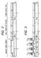
- FIGS. 2 through 15 and FIGS. 17 to 19are diagrams which illustrate, in cross-section, some of the major steps in the manufacture of a DRAM embodying the invention.
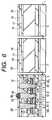
- FIG. 16is a diagram which depicts a plan view of a pattern of a resin layer as formed in a scribe region SR.
- FIG.1is a diagram showing a plan view of part (one chip region 1 A and its surrounding scribe region SR) of a semiconductor wafer 1 on which a DRAM embodying the invention is formed.
- multiple memory arrays-MARYare laid out,each of which includes rows and columns of memory cells arranged in the form of a matrix.
- fuses (second fuses) Fbare preformed for use in changing or “switching” defective cells, which may be produced within the memory arrays MARY during manufacturing processes, to one or more redundant cells.
- peripheral circuitryincluding word drivers WD and redundant circuits RC and bonding pads BP are disposed at the center of the principal surface of the chip region 1 A.
- a TEGis laid out in the scribe region SR along the periphery of the chip region 1 A, at part of which test-use or “testing” pads TP are formed along with a fuse Fa (first fuse) as electrically connected thereto.
- FIGS. 2 to 19A method of manufacturing the DRAM will next be explained by reference to FIGS. 2 to 19 .
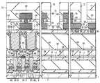
- the left-hand partrepresents a portion (first region) of the memory array (MARY)
- the central partindicates a region (second region) reserved for fabrication of the fuses Fb
- the right-hand partshows the scribe region SR.
- an element isolation groove 6is formed in the principal surface of the semiconductor substrate (wafer) 1 made for example of single-crystalline silicon of p type conductivity; and, thereafter, the semiconductor substrate 1 is doped by ion implantation techniques with a chosen impurity to thereby form therein a p-type well 2 and n-type well 4 . Additionally an n-type semiconductor region 3 is formed at the lower part of the p-type well 3 of the memory arrays for purposes of preventing unwanted immersion or “invasion” of noises from input/output circuitry formed in other regions of the semiconductor substrate 1 .
- an impurityis doped into the p-type well 2 and n-type well 4 for use in adjustment of the threshold voltage of MISFETs, such as BF 2 (boron fluoride) by way of example; and, then, after using HF (hydrofluoric acid) based cleaning fluid to clean the surfaces of the p-type well 2 and n-type well 4 , the semiconductor substrate 1 is subject to wet oxidation processing,thereby forming a clean gate oxide film 7 on the surface of an active region or regions.
- MISFETssuch as BF 2 (boron fluoride)
- a gate electrode 8(word line WL) is fabricated on the gate oxide film 7 .
- the gate oxide film 8(word line WL) is typically formed by a method including,for-example,the steps of depositing by chemical vapor deposition (CVD) techniques an n-type impurity-doped polycrystalline silicon film on or over the semiconductor substrate 1 , depositing by sputtering methods a WN (tungsten nitride) film and W film thereon, further depositing thereon a silicon nitride film 12 using CVD techniques, and then patterning these films with a photoresist film being used as a mask therefor.
- CVDchemical vapor deposition
- ion implantationis used to dope an n-type TiN film and Ta 2 O 5 film 46 , to thereby form an impurity into the p-type well 2 to form n ⁇ -type semiconductor regions 9 a in the p-type well 2 at locations lying between adjacent ones of patterned insulated gate electrodes 8 .
- MISFETs Qsare formed for use in selecting memory cells in the illustrated memory array.
- a silicon nitride film 13is deposited by CVD methods on the semiconductor substrate 1 ; then, selected portions of the silicon nitride film 13 residing in regions other than the memory array are removed through etching treatment; and, thereafter, the semiconductor substrate 1 is spin-coated with an SOG film 16 .
- a silicon oxide film 17is deposited over the SOG film 16 ; and, then, after having planarized the surface of this silicon oxide film 17 by chemical/mechanical polishing (CMP) techniques, a silicon oxide film 18 is deposited thereon.
- the silicon oxide film 18is deposited in order to repair ultrafine injuries or “scars” in the surface of the silicon oxide film 17 which can occur during the CMP process.
- those portions of the silicon oxide film 18 overlying the n ⁇ -type semiconductor regions (source, drain) 9 a of memory cell-select MISFETs Qsare removed, while further removing the underlying silicon nitride film 13 ,to thereby form a contact hole 19 overlying one of the n ⁇ -type semiconductor regions (source, drain) 9 a with a contact hole 20 formed at a location overlying the other.
- plugs 21are formed inside of the contact holes 19 , 20 .
- the plugs 21are formed by, for example, depositing by CVD methods a polycrystalline silicon film with an n-type impurity doped therein on the silicon oxide film 18 , and then polishing this polycrystalline silicon film by CMP techniques thus causing it to reside within the contact holes 19 , 20 .
- a silicon oxide film 28is deposited on the silicon oxide film 18 , part of which overlying the contact hole 19 is then etched away to, define a through-going hole 22 therein; and, thereafter, a plug 35 is fabricated inside of the through-hole 22 .
- the plug 35may typically be formed by depositing a TiN film and W film overlying the silicon oxide film 28 and then removing the W film 41 and TiN film overlying the silicon oxide film 28 using CMP methods. Subsequently, the W film that has been deposited by sputtering methods on the silicon oxide film 28 is patterned forming bit lines BL in the memory arrays involved.
- the silicon oxide film 39is subjected to surface planarization using CMP techniques. Subsequently, etching treatment is applied to the silicon oxide films 38 , 39 overlying the contact hole 20 to form a through-hole 48 ; and, thereafter, within the through-hole 48 a plug 49 is fabricated, which plug is comprised of a polycrystalline silicon film.
- a silicon nitride film 44is deposited by CVD methods on the-silicon oxide film 39 while CVD-depositing a silicon oxide film 50 on the silicon nitride film 44 ; and, thereafter, the silicon oxide film 50 and its underlying silicon nitride film 44 are dry-etched with a photoresist film (not shown) used as-a mask-to thereby form a groove 73 overlying the through-hole 48 .
- a lower-side electrode 45 of an information storage capacitive element C to be later discussedis formed along inner walls of this groove 73 , which is required in order to increase the carrier storage amount that the silicon oxide film 50 be deposited to an increased thickness.
- CVD techniquesare used to deposit, on or over the silicon oxide film 50 having the groove 73 , an amorphous silicon film 45 A with an n-type impurity doped thereinto.
- This amorphous silicon film 45 Awill be used as a lower-side electrode material of the information storage capacitor element C.
- the amorphous silicon film 45 A overlying the silicon oxide film 50the resultant surface of the amorphous silicon film 45 A residing inside of the groove 73 is cleaned using hydrofluoric acid-based cleaning fluid.
- the lower electrode 45may alternatively be made of conductive materials other than polycrystalline silicon, such as for example high-melting-point metals including Ru (ruthenium) or conductive metal oxide materials including RuO (ruthenium oxide) and IrO (iridium oxide) or other similar suitable materials.
- a Ta 2 O 5 film 46is deposited, which is then thermally processed at high temperatures in an oxidizing atmosphere to improve the film quality thereof.
- a TiN filmis deposited overlying the Ta 2 O 5 film 46 ; then, a photoresist film (not shown) is used as a mask to effectuate dry etching for patterning of the TiN film and Ta 2 O 5 film 46 , to thereby form an information storage capacitor element C which is comprised of an upper electrode 47 made of the TiN film and a capacitance dielectric film formed of the Ta 2 O 5 film 46 , as well as the lower electrode 45 made of polycrystalline silicon film.
- the TiN film (and the Ta 2 O 5 film 46 ) in a fuse formation regionis simultaneously patterned to fabricate more than one fuse Fb (fuse element) made of the TiN film.
- patterning of the TiN film (and Ta 2 O 5 film 46 ) in the scribe region SRalso results in fabrication of a fuse Fa (conductive layer) made of such a TiN film.
- the Ta 2 O 5 film 46is deposited by CVD techniques using pentaethoxytantalum (Ta(OC 2 H 5 ) 5 ) as a source gas, for example,whereas the TiN film is deposited by use of CVD and sputtering methods in combination.
- pentaethoxytantalumTi(OC 2 H 5 ) 5
- the intended memory cellshave been completed, each of which consists essentially of a memory cell-select MISFET Qs and information storing capacitive element C serially connected thereto.
- the capacitance dielectric film of the information storage capacitor element Cmay alternatively be made of high (strong) dielectric films formed of chosen metal oxides including, but not limited to, BST, STO, BaTiO 3 (barium titanate), PbTiO 3 (lead titanate), PZT (PbZr x Ti 1 ⁇ x O 3 ), PLT (PbLa x Ti 1 ⁇ x O 3 ), and PLZT.
- the upper electrode 47may be conductive films other than the TiN film—for instance, a W film or the like.
- a silicon oxide film 51is deposited by CVD techniques on the information storage capacitor element C, and is then polished by. CMP methods for surface planarization; and, thereafter, a silicon oxide film 52 is CVD-deposited thereon.
- An insulative film to be deposited overlying the information storage capacitor element Cmay consist of a single-layered silicon oxide film 51 only.
- the silicon oxide films 52 , 51 in the scribe region SRare etched with a photoresist film (not shown) used as a mask to thereby define a through-hole 55 overlying the fuse Fa; and, thereafter, a plug 56 is formed inside of the through-hole 55 .
- the plug 56is typically formed by deposition, using sputtering techniques, of a Ti film on the silicon oxide film 52 , further depositing thereon a TiN film and a W film by CVD methods, and then etching back these films to retain those portions which reside within the through-hole 55 .
- second-layered electrical lead patterns 53 , 54 , 57 , 58 , 59are formed on the silicon oxide film 52 .
- Certain leads 58 , 59 of such second-layer leads 53 , 54 , 57 , 58 , 59 which are formed in the scribe region SRare electrically connected to the fuse Fa via the through-hole 55 .
- the second-layer leads 53 , 54 , 57 , 58 , 59may be fabricated by sequentially depositing on the silicon oxide film 52 a TiN film, Al (aluminum) alloy film, Ti film, and TiN film using sputtering techniques, and by patterning these films by dry etching with a photoresist film used as a mask therefor, by way of example.
- a photoresist film(not shown) is used as a mask to etch the silicon oxide films 60 , 61 to thereby form a through-hole 62 overlying the lead 53 of the memory array (MARY) while forming through-holes 63 , 64 overlying the leads 54 , 57 in the fuse formation region and also forming a through-hole 65 overlying the lead 58 in the scribe region SR.
- plugs 66are fabricated inside of the through-holes 62 - 65 .
- the plugs 66are typically formed by depositing a Ti film on the silicon oxide film 61 , using sputtering techniques, further depositing thereon a TiN film and W film by CVD methods, and then etching back these films to retain portions thereof in the through-holes 62 - 65 .
- third-layered leads(uppermost-layer leads) 67 , 68 , 69 , 70 are formed on the silicon oxide film 61 .
- the third-layer leads 62 - 70are formed by, for example, sequentially depositing on the silicon oxide film 61 a TiN film, Al (aluminum) alloy film, Ti film and TiN film by sputtering methods, and then these films are patterned through dry etching with a photoresist film used as a mask.
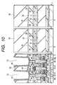
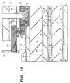
- FIG. 14is an enlarged cross-sectional diagram of the scribe region SR for indicating the third-layer lead 70 that is electrically connected to a fuse Fa via the through-hole 65 and second-layer lead 58 plus through-hole 55 .
- a passivation film 71is deposited on the third-layer leads (uppermost-layer leads) 62 - 70 .
- the passivation film 71is comprised of a lamination of a silicon oxide film and silicon nitride film deposited by plasma CVD techniques as an example.
- a photosensitive polyimide resin materialis deposited on the passivation film 71 ; then, a photomask with a predefined pattern formed therein is used to subject the photosensitive polyimide resin to exposure treatment and then development processing in this order, thereby forming on the passivation film 71 a resin layer 72 which is opened in specified regions.
- the resin layer 72is such that openings (first openings) 73 are formed overlying the fuses Fb formed in the fuse formation region.
- the resin layer 72has openings or holes which are formed overlying selected regions in which the bonding pads BP within the chip region 1 A are formed (see FIG. 1 ).
- FIG. 16is a diagram showing a planar pattern of the resin layer formed in the scribe region SR; while, FIG. 17 depicts a cross-section of the layer taken along line a-a′ of FIG. 16 .
- the resin layer 72 in the scribe region SRis selectively formed only at portions overlying those conductive layers that overlie the fuse Fa—namely over the plug 56 formed inside of the through-hole 55 , the second-layer leads 58 - 59 , the plug 66 formed within the through-hole 65 , and the third-layer lead 70 —and is not formed in any of the remaining regions.
- the resin layer 72 coveringterminate ends of-the third-layer lead 70 has openings or apertures formed therein for forming the testing pads TP.
- the above-noted pattern of the resin layer 72may be formed by a method including the steps of applying OR processing to the patterns of specific conductive layers overlying the fuse Fa, i.e. the plug 56 , second-layer leads 58 - 59 , plug 66 and third-layer lead 70 , fabricating a combined or “synthetic” pattern along with an opening 74 pattern for use in forming the testing pads TP, and forming this synthetic pattern in a photomask for effectuation of the intended exposure and development processes of a photosensitive polyimide resin.
- this synthetic patternwill be desirable when forming this synthetic pattern that, in view of possible position alignment deviation between different conductive layers such as the plug 56 , second-layer leads 58 - 59 , plug 66 , third-layer lead 70 and opening 74 , the synthetic pattern be subjected to size enlargement (broadening) processing to absorb such alignment deviation therebetween.
- the resin layer 72is used as a mask to dry-etch the passivation film 71 thereby forming an opening 75 which overlies the defect-curing fuse Fb that was formed in the fuse formation region while simultaneously forming one or more testing pads TP in the scribe region SR with more than one bonding pad BP being formed in the chip region 1 A.
- the fuse elementbe constituted from the upper electrode of a capacitive element makes it possible to reduce the resultant aspect ratio of the opening 75 , which may in turn facilitate fabrication of the opening 75 . Additionally, the production yields may also be improved.
- each such openingis limited in depth so that it does not reach the fuse Fa. Accordingly, in the scribe region SR, those conductive layers forming fuses Fa and their underlying conductive layer(s) are free from any damage occurring due to dry etching during formation of the openings or apertures. In other words, it is possible in the scribe region SR to freely use the conductive layers forming the fuses Fa and their underlying conductive layer(s) while allowing the photosensitive polyimide resin layer 72 to no longer cover these conductive layer. This makes it possible to improve the lead layout flexibility in the scribe region SR while at the same time reducing the requisite area of photosensitive polyimide resin layer 72 .
- a dicing blade instrumentsuch as a dicing cutter, is used to saw the scribe region SR of the semiconductor wafer 1 thereby cutting the wafer 1 into small square chips, or dice.
- a dicing blade instrumentsuch as a dicing cutter, is used to saw the scribe region SR of the semiconductor wafer 1 thereby cutting the wafer 1 into small square chips, or dice.
- the fusesare formed using the upper electrode material of an information storing capacitance element
- the fusesmay alternatively be modified so that they employ other similar suitable electrode lead materials including but not limited to high-melting-point metal silicide.
- the inventionmay also be applicable to fuse-opening formation processes of those LSIs other than DRAMs, such as static RAMs (SRAMs), nonvolatile memories, and the like.
- the present inventionit is possible to successfully prevent any possible destruction of the TEG as formed in scribe regions while simultaneously suppressing lifetime reduction of a dicing blade instrument used for cutting a wafer into chips.
- a resin layer, deposited on or over the wafer surface, which is made of photosensitive polyimide resin materialsmakes it possible to reduce the requisite number of wafer processing steps. It is thus possible to reduce or minimize production costs of intended semiconductor integrated circuit devices.
Landscapes
- Engineering & Computer Science (AREA)
- Physics & Mathematics (AREA)
- Condensed Matter Physics & Semiconductors (AREA)
- General Physics & Mathematics (AREA)
- Computer Hardware Design (AREA)
- Microelectronics & Electronic Packaging (AREA)
- Power Engineering (AREA)
- Manufacturing & Machinery (AREA)
- Design And Manufacture Of Integrated Circuits (AREA)
- Semiconductor Memories (AREA)
Abstract
Description
Claims (21)
Applications Claiming Priority (2)
| Application Number | Priority Date | Filing Date | Title |
|---|---|---|---|
| JP25160998AJP4322330B2 (en) | 1998-09-04 | 1998-09-04 | Manufacturing method of semiconductor integrated circuit device |
| JP10-251609 | 1998-09-04 |
Publications (1)
| Publication Number | Publication Date |
|---|---|
| US6372554B1true US6372554B1 (en) | 2002-04-16 |
Family
ID=17225371
Family Applications (1)
| Application Number | Title | Priority Date | Filing Date |
|---|---|---|---|
| US09/390,682Expired - LifetimeUS6372554B1 (en) | 1998-09-04 | 1999-09-07 | Semiconductor integrated circuit device and method for production of the same |
Country Status (4)
| Country | Link |
|---|---|
| US (1) | US6372554B1 (en) |
| JP (1) | JP4322330B2 (en) |
| KR (1) | KR20000022792A (en) |
| TW (1) | TW463320B (en) |
Cited By (54)
| Publication number | Priority date | Publication date | Assignee | Title |
|---|---|---|---|---|
| US20020153539A1 (en)* | 2001-04-23 | 2002-10-24 | Toshio Miyamoto | Semiconductor integrated circuit device and method of manufacturing the same |
| US6586282B1 (en)* | 1999-05-11 | 2003-07-01 | Seiko Instruments Inc. | Method of manufacturing a semiconductor device |
| US20030128615A1 (en)* | 2001-01-05 | 2003-07-10 | Micron Technology, Inc. | Integrated circuit having aligned fuses and methods for forming and programming the fuses |
| US20030146514A1 (en)* | 2002-02-01 | 2003-08-07 | Mitsubishi Denki Kabushiki Kaisha And Ryoden Semiconductor System Engineering Corporation | Semiconductor device and method of fabricating the same |
| US6611010B2 (en)* | 1999-12-03 | 2003-08-26 | Kabushiki Kaisha Toshiba | Semiconductor device |
| US20030213953A1 (en)* | 2002-05-15 | 2003-11-20 | Kwon-Il Sohn | Integrated circuit chips and wafers including on-chip test element group circuits, and methods of fabricating and testing same |
| US6737743B2 (en)* | 2001-07-10 | 2004-05-18 | Kabushiki Kaisha Toshiba | Memory chip and semiconductor device using the memory chip and manufacturing method of those |
| US20040150051A1 (en)* | 2003-01-30 | 2004-08-05 | Kim Do Woo | SRAM cell and method of manufacturing the same |
| US20040159906A1 (en)* | 2002-05-01 | 2004-08-19 | Shingo Hashimoto | Semiconductor device and blowout method of fuse |
| US6838367B1 (en)* | 2000-08-24 | 2005-01-04 | Micron Technology, Inc. | Method for simultaneous formation of fuse and capacitor plate and resulting structure |
| US20050023260A1 (en)* | 2003-01-10 | 2005-02-03 | Shinya Takyu | Semiconductor wafer dividing apparatus and semiconductor device manufacturing method |
| US6897110B1 (en)* | 2002-11-26 | 2005-05-24 | Advanced Micro Devices, Inc. | Method of protecting a memory array from charge damage during fabrication |
| US20050287780A1 (en)* | 2003-09-04 | 2005-12-29 | Micron Technology, Inc. | Semiconductor constructions |
| US20060014344A1 (en)* | 2004-07-19 | 2006-01-19 | Manning H M | Methods of forming semiconductor structures and capacitor devices |
| US6989577B2 (en)* | 2000-09-14 | 2006-01-24 | Kabushiki Kaisha Toshiba | Semiconductor device having multiple insulation layers |
| US20060017153A1 (en)* | 2004-07-22 | 2006-01-26 | Samsung Electronics Co., Ltd. | Interconnections of semiconductor device and method of forming the same |
| US20060046420A1 (en)* | 2004-08-27 | 2006-03-02 | Manning H M | Methods of forming a plurality of capacitors |
| US20060113547A1 (en)* | 2004-11-29 | 2006-06-01 | Samsung Electronics Co., Ltd. | Methods of fabricating memory devices including fuses and load resistors in a peripheral circuit region |
| US20060148190A1 (en)* | 2004-08-30 | 2006-07-06 | Busch Brett W | Methods of forming a plurality of capacitors |
| US20060170528A1 (en)* | 2005-01-28 | 2006-08-03 | Yasuhiro Fukushige | Dual fuse link thin film fuse |
| US20060211211A1 (en)* | 2005-03-18 | 2006-09-21 | Sandhu Gurtej S | Methods of forming pluralities of capacitors |
| US20060256597A1 (en)* | 2005-05-13 | 2006-11-16 | Stmicroelectronics S.R.L | Method and relative circuit for generating a control voltage of a synchronous rectifier |
| US20060263968A1 (en)* | 2005-05-18 | 2006-11-23 | Micron Technology, Inc. | Methods of forming pluralities of capacitors |
| US20060261440A1 (en)* | 2005-05-18 | 2006-11-23 | Micron Technology, Inc. | Methods of forming a plurality of capacitors, and integrated circuitry comprising a pair of capacitors |
| US20060273371A1 (en)* | 2005-06-07 | 2006-12-07 | Matsushita Electric Industrial Co., Ltd. | Evaluation semiconductor device |
| US20070093022A1 (en)* | 2004-12-06 | 2007-04-26 | Cem Basceri | Integrated circuitry |
| US20070105303A1 (en)* | 2004-08-27 | 2007-05-10 | Busch Brett W | Methods of forming a plurality of circuit components and methods of forming a plurality of structures suspended elevationally above a substrate |
| US20070126084A1 (en)* | 2005-12-01 | 2007-06-07 | Samsung Electronics Co., Ltd. | Semiconductor device including fuse focus detector, fabrication method thereof and laser repair method using the fuse detector |
| US20070134872A1 (en)* | 2005-08-02 | 2007-06-14 | Sandhu Gurtej S | Methods of forming pluralities of capacitors |
| US20070238259A1 (en)* | 2006-04-10 | 2007-10-11 | Micron Technology, Inc. | Methods of forming a plurality of capacitors |
| US20080012070A1 (en)* | 2005-07-08 | 2008-01-17 | Werner Juengling | Apparatus for a self-aligned recessed access device (rad) transistor gate |
| US20080054263A1 (en)* | 2006-09-04 | 2008-03-06 | Samsung Electronics Co., Ltd. | Semiconductor device and method of fabricating the same |
| US20080090416A1 (en)* | 2006-10-11 | 2008-04-17 | Micro Technology, Inc. | Methods of etching polysilicon and methods of forming pluralities of capacitors |
| US20080206950A1 (en)* | 2007-02-26 | 2008-08-28 | Micron Technology, Inc. | Methods of forming a plurality of capacitors |
| US20090176011A1 (en)* | 2008-01-08 | 2009-07-09 | Mark Kiehlbauch | Capacitor Forming Methods |
| US20090239343A1 (en)* | 2006-07-17 | 2009-09-24 | Fernando Gonzalez | Methods Of Forming Lines Of Capacitorless One Transistor DRAM Cells, Methods Of Patterning Substrates, And Methods Of Forming Two Conductive Lines |
| US20090251845A1 (en)* | 2008-04-08 | 2009-10-08 | Micron Technology, Inc. | High aspect ratio openings |
| US20100009512A1 (en)* | 2008-07-09 | 2010-01-14 | Fred Fishburn | Methods of forming a plurality of capacitors |
| US7655968B2 (en) | 2003-09-04 | 2010-02-02 | Micron Technology, Inc. | Semiconductor devices |
| US7682924B2 (en) | 2007-08-13 | 2010-03-23 | Micron Technology, Inc. | Methods of forming a plurality of capacitors |
| US20110012182A1 (en)* | 2004-09-01 | 2011-01-20 | Micron Technology Inc. | Semiconductor Constructions and Transistors, and Methods of Forming Semiconductor Constructions and Transistors |
| US20110086476A1 (en)* | 2005-08-30 | 2011-04-14 | Micron Technology, Inc. | Methods of Forming Field Effect Transistors on Substrates |
| US20110124168A1 (en)* | 2006-02-02 | 2011-05-26 | Micron Technology, Inc. | Methods of Forming Field Effect Transistors, Methods of Forming Field Effect Transistor Gates, Methods of Forming Integrated Circuitry Comprising a Transistor Gate Array and Circuitry Peripheral to the Gate Array, and Methods of Forming Integrated Circuitry Comprising a Transistor Gate Array Including First Gates and Second Grounded Isolation Gates |
| US20110175192A1 (en)* | 2008-03-11 | 2011-07-21 | Hynix Semiconductor Inc. | Semiconductor device and method for fabricating the same |
| US8394699B2 (en) | 2006-08-21 | 2013-03-12 | Micron Technology, Inc. | Memory arrays and methods of fabricating memory arrays |
| US8446762B2 (en) | 2006-09-07 | 2013-05-21 | Micron Technology, Inc. | Methods of making a semiconductor memory device |
| US8518788B2 (en) | 2010-08-11 | 2013-08-27 | Micron Technology, Inc. | Methods of forming a plurality of capacitors |
| US8652926B1 (en) | 2012-07-26 | 2014-02-18 | Micron Technology, Inc. | Methods of forming capacitors |
| CN103681555A (en)* | 2012-08-29 | 2014-03-26 | 台湾积体电路制造股份有限公司 | Structure to increase resistance to electromigration |
| US8946043B2 (en) | 2011-12-21 | 2015-02-03 | Micron Technology, Inc. | Methods of forming capacitors |
| US9076680B2 (en) | 2011-10-18 | 2015-07-07 | Micron Technology, Inc. | Integrated circuitry, methods of forming capacitors, and methods of forming integrated circuitry comprising an array of capacitors and circuitry peripheral to the array |
| US10515801B2 (en) | 2007-06-04 | 2019-12-24 | Micron Technology, Inc. | Pitch multiplication using self-assembling materials |
| US20210126041A1 (en)* | 2018-07-12 | 2021-04-29 | Shenzhen Xpectvision Technology Co., Ltd. | Methods of making a radiation detector |
| CN115802745A (en)* | 2022-11-21 | 2023-03-14 | 长鑫存储技术有限公司 | Manufacturing method of semiconductor device, semiconductor device and DRAM |
Families Citing this family (1)
| Publication number | Priority date | Publication date | Assignee | Title |
|---|---|---|---|---|
| CN114975485B (en)* | 2022-06-14 | 2024-08-13 | 福建华佳彩有限公司 | Preparation method for improving silicon oxide cracking and pinholes of metal oxide insulating layer |
Citations (7)
| Publication number | Priority date | Publication date | Assignee | Title |
|---|---|---|---|---|
| JPH0225055A (en) | 1988-07-13 | 1990-01-26 | Hitachi Ltd | Semiconductor memory device |
| US5627400A (en)* | 1994-08-01 | 1997-05-06 | Nec Corporation | Semiconductor memory device |
| US5891762A (en)* | 1995-08-07 | 1999-04-06 | Matsushita Electronics Corporation | Method of forming a semiconductor device by using a conductive film as an etching stopper |
| US5972756A (en)* | 1995-11-30 | 1999-10-26 | Mitsubishi Denki Kabushiki Kaisha | Method of fabricating semiconductor device with a fuse portion |
| US6100117A (en)* | 1998-03-20 | 2000-08-08 | Nanya Technology Corp. | Method for manufacturing DRAM having a redundancy circuit region |
| US6124165A (en)* | 1999-05-26 | 2000-09-26 | Vanguard International Semiconductor Corporation | Method for making openings in a passivation layer over polycide fuses using a single mask while forming reliable tungsten via plugs on DRAMs |
| US6180503B1 (en)* | 1999-07-29 | 2001-01-30 | Vanguard International Semiconductor Corporation | Passivation layer etching process for memory arrays with fusible links |
- 1998
- 1998-09-04JPJP25160998Apatent/JP4322330B2/ennot_activeExpired - Fee Related
- 1999
- 1999-08-30KRKR1019990036295Apatent/KR20000022792A/ennot_activeCeased
- 1999-09-07USUS09/390,682patent/US6372554B1/ennot_activeExpired - Lifetime
- 2000
- 2000-03-02TWTW088115300Apatent/TW463320B/enactive
Patent Citations (7)
| Publication number | Priority date | Publication date | Assignee | Title |
|---|---|---|---|---|
| JPH0225055A (en) | 1988-07-13 | 1990-01-26 | Hitachi Ltd | Semiconductor memory device |
| US5627400A (en)* | 1994-08-01 | 1997-05-06 | Nec Corporation | Semiconductor memory device |
| US5891762A (en)* | 1995-08-07 | 1999-04-06 | Matsushita Electronics Corporation | Method of forming a semiconductor device by using a conductive film as an etching stopper |
| US5972756A (en)* | 1995-11-30 | 1999-10-26 | Mitsubishi Denki Kabushiki Kaisha | Method of fabricating semiconductor device with a fuse portion |
| US6100117A (en)* | 1998-03-20 | 2000-08-08 | Nanya Technology Corp. | Method for manufacturing DRAM having a redundancy circuit region |
| US6124165A (en)* | 1999-05-26 | 2000-09-26 | Vanguard International Semiconductor Corporation | Method for making openings in a passivation layer over polycide fuses using a single mask while forming reliable tungsten via plugs on DRAMs |
| US6180503B1 (en)* | 1999-07-29 | 2001-01-30 | Vanguard International Semiconductor Corporation | Passivation layer etching process for memory arrays with fusible links |
Cited By (135)
| Publication number | Priority date | Publication date | Assignee | Title |
|---|---|---|---|---|
| US6586282B1 (en)* | 1999-05-11 | 2003-07-01 | Seiko Instruments Inc. | Method of manufacturing a semiconductor device |
| US6611010B2 (en)* | 1999-12-03 | 2003-08-26 | Kabushiki Kaisha Toshiba | Semiconductor device |
| US6838367B1 (en)* | 2000-08-24 | 2005-01-04 | Micron Technology, Inc. | Method for simultaneous formation of fuse and capacitor plate and resulting structure |
| US6989577B2 (en)* | 2000-09-14 | 2006-01-24 | Kabushiki Kaisha Toshiba | Semiconductor device having multiple insulation layers |
| US6784043B2 (en)* | 2001-01-05 | 2004-08-31 | Micron Technology, Inc. | Methods for forming aligned fuses disposed in an integrated circuit |
| US20030128615A1 (en)* | 2001-01-05 | 2003-07-10 | Micron Technology, Inc. | Integrated circuit having aligned fuses and methods for forming and programming the fuses |
| US20040227254A1 (en)* | 2001-04-23 | 2004-11-18 | Toshio Miyamoto | Semiconductor integrated circuit device and method of manufacturing the same |
| US20020153539A1 (en)* | 2001-04-23 | 2002-10-24 | Toshio Miyamoto | Semiconductor integrated circuit device and method of manufacturing the same |
| US6720591B2 (en)* | 2001-04-23 | 2004-04-13 | Renesas Technology Corp. | Semiconductor integrated circuit device |
| US6949416B2 (en) | 2001-04-23 | 2005-09-27 | Renesas Technology Corp. | Method of manufacturing a semiconductor integrated circuit device |
| US20050116315A1 (en)* | 2001-05-24 | 2005-06-02 | Shingo Hashimoto | Semiconductor device and blowout method of fuse |
| US6972474B2 (en) | 2001-05-24 | 2005-12-06 | Nec Electronics Corporation | Semiconductor device having a fuse and a low heat conductive section for blowout of fuse |
| US7977159B2 (en) | 2001-07-10 | 2011-07-12 | Kabushiki Kaisha Toshiba | Memory chip and semiconductor device using the memory chip and manufacturing method of those |
| US6737743B2 (en)* | 2001-07-10 | 2004-05-18 | Kabushiki Kaisha Toshiba | Memory chip and semiconductor device using the memory chip and manufacturing method of those |
| US20060148130A1 (en)* | 2001-07-10 | 2006-07-06 | Yukihiro Urakawa | Memory chip and semiconductor device using the memory chip and manufacturing method of those |
| US7466029B2 (en) | 2001-07-10 | 2008-12-16 | Kabushiki Kaisha Toshiba | Chip on chip device including basic chips capable of functioning independently from each other, and a system in package device including the chip on chip device |
| US6815265B2 (en)* | 2002-02-01 | 2004-11-09 | Renesas Technology Corp. | Method of fabricating a semiconductor device with a passivation film |
| US20030146514A1 (en)* | 2002-02-01 | 2003-08-07 | Mitsubishi Denki Kabushiki Kaisha And Ryoden Semiconductor System Engineering Corporation | Semiconductor device and method of fabricating the same |
| US20040159906A1 (en)* | 2002-05-01 | 2004-08-19 | Shingo Hashimoto | Semiconductor device and blowout method of fuse |
| US20030213953A1 (en)* | 2002-05-15 | 2003-11-20 | Kwon-Il Sohn | Integrated circuit chips and wafers including on-chip test element group circuits, and methods of fabricating and testing same |
| US7307441B2 (en) | 2002-05-15 | 2007-12-11 | Samsung Electronics Co., Ltd. | Integrated circuit chips and wafers including on-chip test element group circuits, and methods of fabricating and testing same |
| US6897110B1 (en)* | 2002-11-26 | 2005-05-24 | Advanced Micro Devices, Inc. | Method of protecting a memory array from charge damage during fabrication |
| US20050023260A1 (en)* | 2003-01-10 | 2005-02-03 | Shinya Takyu | Semiconductor wafer dividing apparatus and semiconductor device manufacturing method |
| US6902963B2 (en)* | 2003-01-30 | 2005-06-07 | Hynix Semiconductor Inc. | SRAM cell and method of manufacturing the same |
| US20040150051A1 (en)* | 2003-01-30 | 2004-08-05 | Kim Do Woo | SRAM cell and method of manufacturing the same |
| US8786001B2 (en) | 2003-09-04 | 2014-07-22 | Round Rock Research, Llc | Semiconductor devices |
| US7420238B2 (en) | 2003-09-04 | 2008-09-02 | Micron Technology, Inc. | Semiconductor constructions |
| US20050287780A1 (en)* | 2003-09-04 | 2005-12-29 | Micron Technology, Inc. | Semiconductor constructions |
| US7449391B2 (en) | 2003-09-04 | 2008-11-11 | Micron Technology, Inc. | Methods of forming plurality of capacitor devices |
| US20100117196A1 (en)* | 2003-09-04 | 2010-05-13 | Manning Homer M | Support For Vertically-Oriented Capacitors During The Formation of a Semiconductor Device |
| US7655968B2 (en) | 2003-09-04 | 2010-02-02 | Micron Technology, Inc. | Semiconductor devices |
| US7585741B2 (en) | 2004-07-19 | 2009-09-08 | Micron Technology, Inc. | Methods of forming capacitors |
| US20060249798A1 (en)* | 2004-07-19 | 2006-11-09 | Manning H M | Methods of forming capacitors |
| US8164132B2 (en) | 2004-07-19 | 2012-04-24 | Round Rock Research, Llc | Methods of forming integrated circuit devices |
| US20090286377A1 (en)* | 2004-07-19 | 2009-11-19 | Micron Technology, Inc | Methods of Forming Integrated Circuit Devices |
| US20110186964A1 (en)* | 2004-07-19 | 2011-08-04 | Round Rock Research, Llc | Methods of forming integrated circuit devices |
| US7387939B2 (en) | 2004-07-19 | 2008-06-17 | Micron Technology, Inc. | Methods of forming semiconductor structures and capacitor devices |
| US20060014344A1 (en)* | 2004-07-19 | 2006-01-19 | Manning H M | Methods of forming semiconductor structures and capacitor devices |
| US7915136B2 (en) | 2004-07-19 | 2011-03-29 | Round Rock Research, Llc | Methods of forming integrated circuit devices |
| US20060017153A1 (en)* | 2004-07-22 | 2006-01-26 | Samsung Electronics Co., Ltd. | Interconnections of semiconductor device and method of forming the same |
| US7445991B2 (en) | 2004-08-27 | 2008-11-04 | Micron Technology, Inc. | Methods of forming a plurality of capacitors |
| US20070173030A1 (en)* | 2004-08-27 | 2007-07-26 | Micron Technology, Inc. | Methods of forming a plurality of capacitors |
| US20070161202A1 (en)* | 2004-08-27 | 2007-07-12 | Manning H M | Methods of forming a plurality of capacitors |
| US20060046420A1 (en)* | 2004-08-27 | 2006-03-02 | Manning H M | Methods of forming a plurality of capacitors |
| US20070105303A1 (en)* | 2004-08-27 | 2007-05-10 | Busch Brett W | Methods of forming a plurality of circuit components and methods of forming a plurality of structures suspended elevationally above a substrate |
| US7439152B2 (en) | 2004-08-27 | 2008-10-21 | Micron Technology, Inc. | Methods of forming a plurality of capacitors |
| US7534694B2 (en) | 2004-08-27 | 2009-05-19 | Micron Technology, Inc. | Methods of forming a plurality of capacitors |
| US20060246678A1 (en)* | 2004-08-27 | 2006-11-02 | Manning H M | Methods of forming a plurality of capacitors |
| US7393743B2 (en) | 2004-08-27 | 2008-07-01 | Micron Technology, Inc. | Methods of forming a plurality of capacitors |
| US7413952B2 (en) | 2004-08-27 | 2008-08-19 | Micron Technology, Inc. | Methods of forming a plurality of circuit components and methods of forming a plurality of structures suspended elevationally above a substrate |
| US20060148190A1 (en)* | 2004-08-30 | 2006-07-06 | Busch Brett W | Methods of forming a plurality of capacitors |
| US7445990B2 (en) | 2004-08-30 | 2008-11-04 | Micron Technology, Inc. | Methods of forming a plurality of capacitors |
| US8120101B2 (en) | 2004-09-01 | 2012-02-21 | Micron Technology, Inc. | Semiconductor constructions and transistors, and methods of forming semiconductor constructions and transistors |
| US20110012182A1 (en)* | 2004-09-01 | 2011-01-20 | Micron Technology Inc. | Semiconductor Constructions and Transistors, and Methods of Forming Semiconductor Constructions and Transistors |
| US20060113547A1 (en)* | 2004-11-29 | 2006-06-01 | Samsung Electronics Co., Ltd. | Methods of fabricating memory devices including fuses and load resistors in a peripheral circuit region |
| US20070093022A1 (en)* | 2004-12-06 | 2007-04-26 | Cem Basceri | Integrated circuitry |
| US8207563B2 (en) | 2004-12-06 | 2012-06-26 | Round Rock Research, Llc | Integrated circuitry |
| US7477130B2 (en) | 2005-01-28 | 2009-01-13 | Littelfuse, Inc. | Dual fuse link thin film fuse |
| US20060170528A1 (en)* | 2005-01-28 | 2006-08-03 | Yasuhiro Fukushige | Dual fuse link thin film fuse |
| US20090209080A1 (en)* | 2005-03-18 | 2009-08-20 | Sandhu Gurtej S | Methods of Forming Pluralities of Capacitors |
| US7557015B2 (en) | 2005-03-18 | 2009-07-07 | Micron Technology, Inc. | Methods of forming pluralities of capacitors |
| US7919386B2 (en) | 2005-03-18 | 2011-04-05 | Micron Technology, Inc. | Methods of forming pluralities of capacitors |
| US20060211211A1 (en)* | 2005-03-18 | 2006-09-21 | Sandhu Gurtej S | Methods of forming pluralities of capacitors |
| US20060256597A1 (en)* | 2005-05-13 | 2006-11-16 | Stmicroelectronics S.R.L | Method and relative circuit for generating a control voltage of a synchronous rectifier |
| US20060263968A1 (en)* | 2005-05-18 | 2006-11-23 | Micron Technology, Inc. | Methods of forming pluralities of capacitors |
| US20070196978A1 (en)* | 2005-05-18 | 2007-08-23 | Manning H M | Integrated circuitry comprising a pair of adjacent capacitors |
| US7825451B2 (en) | 2005-05-18 | 2010-11-02 | Micron Technology, Inc. | Array of capacitors with electrically insulative rings |
| US20100261331A1 (en)* | 2005-05-18 | 2010-10-14 | Manning H Montgomery | Methods Of Forming A Plurality Of Capacitors |
| US7517753B2 (en) | 2005-05-18 | 2009-04-14 | Micron Technology, Inc. | Methods of forming pluralities of capacitors |
| US7544563B2 (en) | 2005-05-18 | 2009-06-09 | Micron Technology, Inc. | Methods of forming a plurality of capacitors |
| US20060261440A1 (en)* | 2005-05-18 | 2006-11-23 | Micron Technology, Inc. | Methods of forming a plurality of capacitors, and integrated circuitry comprising a pair of capacitors |
| US7858486B2 (en) | 2005-05-18 | 2010-12-28 | Micron Technology, Inc. | Methods of forming a plurality of capacitors |
| US20060273371A1 (en)* | 2005-06-07 | 2006-12-07 | Matsushita Electric Industrial Co., Ltd. | Evaluation semiconductor device |
| US8916912B2 (en) | 2005-07-08 | 2014-12-23 | Micron Technology, Inc. | Semiconductor device comprising a transistor gate having multiple vertically oriented sidewalls |
| US20080012070A1 (en)* | 2005-07-08 | 2008-01-17 | Werner Juengling | Apparatus for a self-aligned recessed access device (rad) transistor gate |
| US9536971B2 (en) | 2005-07-08 | 2017-01-03 | Micron Technology, Inc. | Semiconductor device comprising a transistor gate having multiple vertically oriented sidewalls |
| US8399920B2 (en) | 2005-07-08 | 2013-03-19 | Werner Juengling | Semiconductor device comprising a transistor gate having multiple vertically oriented sidewalls |
| US20070134872A1 (en)* | 2005-08-02 | 2007-06-14 | Sandhu Gurtej S | Methods of forming pluralities of capacitors |
| US7393741B2 (en) | 2005-08-02 | 2008-07-01 | Micron Technology, Inc. | Methods of forming pluralities of capacitors |
| US20110086476A1 (en)* | 2005-08-30 | 2011-04-14 | Micron Technology, Inc. | Methods of Forming Field Effect Transistors on Substrates |
| US8877589B2 (en) | 2005-08-30 | 2014-11-04 | Micron Technology, Inc. | Methods of forming field effect transistors on substrates |
| US8426273B2 (en) | 2005-08-30 | 2013-04-23 | Micron Technology, Inc. | Methods of forming field effect transistors on substrates |
| US7671361B2 (en)* | 2005-12-01 | 2010-03-02 | Samsung Electronics Co., Ltd | Semiconductor device including fuse focus detector, fabricating method thereof and laser repair method using the fuse focus detector |
| US20070126084A1 (en)* | 2005-12-01 | 2007-06-07 | Samsung Electronics Co., Ltd. | Semiconductor device including fuse focus detector, fabrication method thereof and laser repair method using the fuse detector |
| US8389363B2 (en) | 2006-02-02 | 2013-03-05 | Micron Technology, Inc. | Methods of forming field effect transistors, methods of forming field effect transistor gates, methods of forming integrated circuitry comprising a transistor gate array and circuitry peripheral to the gate array, and methods of forming integrated circuitry comprising a transistor gate array including first gates and second grounded isolation gates |
| US20110124168A1 (en)* | 2006-02-02 | 2011-05-26 | Micron Technology, Inc. | Methods of Forming Field Effect Transistors, Methods of Forming Field Effect Transistor Gates, Methods of Forming Integrated Circuitry Comprising a Transistor Gate Array and Circuitry Peripheral to the Gate Array, and Methods of Forming Integrated Circuitry Comprising a Transistor Gate Array Including First Gates and Second Grounded Isolation Gates |
| US20070238259A1 (en)* | 2006-04-10 | 2007-10-11 | Micron Technology, Inc. | Methods of forming a plurality of capacitors |
| US7557013B2 (en) | 2006-04-10 | 2009-07-07 | Micron Technology, Inc. | Methods of forming a plurality of capacitors |
| US20090239343A1 (en)* | 2006-07-17 | 2009-09-24 | Fernando Gonzalez | Methods Of Forming Lines Of Capacitorless One Transistor DRAM Cells, Methods Of Patterning Substrates, And Methods Of Forming Two Conductive Lines |
| US8551823B2 (en) | 2006-07-17 | 2013-10-08 | Micron Technology, Inc. | Methods of forming lines of capacitorless one transistor DRAM cells, methods of patterning substrates, and methods of forming two conductive lines |
| US9129847B2 (en) | 2006-07-17 | 2015-09-08 | Micron Technology, Inc. | Transistor structures and integrated circuitry comprising an array of transistor structures |
| US8394699B2 (en) | 2006-08-21 | 2013-03-12 | Micron Technology, Inc. | Memory arrays and methods of fabricating memory arrays |
| US7763887B2 (en)* | 2006-09-04 | 2010-07-27 | Samsung Electronics Co., Ltd. | Semiconductor device and method of fabricating the same |
| US20100279500A1 (en)* | 2006-09-04 | 2010-11-04 | Han Myoung-Hee | Semiconductor device and method of fabricating the same |
| US8071469B2 (en) | 2006-09-04 | 2011-12-06 | Samsung Electronics Co., Ltd. | Semiconductor device and method of fabricating the same |
| US20080054263A1 (en)* | 2006-09-04 | 2008-03-06 | Samsung Electronics Co., Ltd. | Semiconductor device and method of fabricating the same |
| US8446762B2 (en) | 2006-09-07 | 2013-05-21 | Micron Technology, Inc. | Methods of making a semiconductor memory device |
| US7902081B2 (en) | 2006-10-11 | 2011-03-08 | Micron Technology, Inc. | Methods of etching polysilicon and methods of forming pluralities of capacitors |
| US20080090416A1 (en)* | 2006-10-11 | 2008-04-17 | Micro Technology, Inc. | Methods of etching polysilicon and methods of forming pluralities of capacitors |
| US7785962B2 (en) | 2007-02-26 | 2010-08-31 | Micron Technology, Inc. | Methods of forming a plurality of capacitors |
| US8129240B2 (en) | 2007-02-26 | 2012-03-06 | Micron Technology, Inc. | Methods of forming a plurality of capacitors |
| US8263457B2 (en) | 2007-02-26 | 2012-09-11 | Micron Technology, Inc. | Methods of forming a plurality of capacitors |
| US20080206950A1 (en)* | 2007-02-26 | 2008-08-28 | Micron Technology, Inc. | Methods of forming a plurality of capacitors |
| US20100311219A1 (en)* | 2007-02-26 | 2010-12-09 | Micron Technology, Inc. | Methods of Forming a Plurality of Capacitors |
| US10515801B2 (en) | 2007-06-04 | 2019-12-24 | Micron Technology, Inc. | Pitch multiplication using self-assembling materials |
| US20100151653A1 (en)* | 2007-08-13 | 2010-06-17 | Micron Technology, Inc. | Methods Of Forming A Plurality Of Capacitors |
| US8450164B2 (en) | 2007-08-13 | 2013-05-28 | Micron Technology, Inc. | Methods of forming a plurality of capacitors |
| US7682924B2 (en) | 2007-08-13 | 2010-03-23 | Micron Technology, Inc. | Methods of forming a plurality of capacitors |
| US8388851B2 (en) | 2008-01-08 | 2013-03-05 | Micron Technology, Inc. | Capacitor forming methods |
| US9224798B2 (en) | 2008-01-08 | 2015-12-29 | Micron Technology, Inc. | Capacitor forming methods |
| US20090176011A1 (en)* | 2008-01-08 | 2009-07-09 | Mark Kiehlbauch | Capacitor Forming Methods |
| US8734656B2 (en) | 2008-01-08 | 2014-05-27 | Micron Technology, Inc. | Capacitor forming methods |
| US20110175192A1 (en)* | 2008-03-11 | 2011-07-21 | Hynix Semiconductor Inc. | Semiconductor device and method for fabricating the same |
| US8373201B2 (en) | 2008-03-11 | 2013-02-12 | Hynix Semiconductor Inc. | Semiconductor device and method for fabricating the same |
| US9595387B2 (en) | 2008-04-08 | 2017-03-14 | Micron Technology, Inc. | High aspect ratio openings |
| US8274777B2 (en) | 2008-04-08 | 2012-09-25 | Micron Technology, Inc. | High aspect ratio openings |
| US20090251845A1 (en)* | 2008-04-08 | 2009-10-08 | Micron Technology, Inc. | High aspect ratio openings |
| US8760841B2 (en) | 2008-04-08 | 2014-06-24 | Micron Technology, Inc. | High aspect ratio openings |
| US20100266962A1 (en)* | 2008-07-09 | 2010-10-21 | Micron Technology, Inc. | Methods Of Forming A Plurality Of Capacitors |
| US8163613B2 (en) | 2008-07-09 | 2012-04-24 | Micron Technology, Inc. | Methods of forming a plurality of capacitors |
| US7759193B2 (en) | 2008-07-09 | 2010-07-20 | Micron Technology, Inc. | Methods of forming a plurality of capacitors |
| US20100009512A1 (en)* | 2008-07-09 | 2010-01-14 | Fred Fishburn | Methods of forming a plurality of capacitors |
| US8518788B2 (en) | 2010-08-11 | 2013-08-27 | Micron Technology, Inc. | Methods of forming a plurality of capacitors |
| US9076757B2 (en) | 2010-08-11 | 2015-07-07 | Micron Technology, Inc. | Methods of forming a plurality of capacitors |
| US9076680B2 (en) | 2011-10-18 | 2015-07-07 | Micron Technology, Inc. | Integrated circuitry, methods of forming capacitors, and methods of forming integrated circuitry comprising an array of capacitors and circuitry peripheral to the array |
| US8946043B2 (en) | 2011-12-21 | 2015-02-03 | Micron Technology, Inc. | Methods of forming capacitors |
| US9196673B2 (en) | 2012-07-26 | 2015-11-24 | Micron Technology, Inc. | Methods of forming capacitors |
| US8652926B1 (en) | 2012-07-26 | 2014-02-18 | Micron Technology, Inc. | Methods of forming capacitors |
| CN103681555B (en)* | 2012-08-29 | 2016-10-05 | 台湾积体电路制造股份有限公司 | Increase the structure to electromigratory resistance |
| CN103681555A (en)* | 2012-08-29 | 2014-03-26 | 台湾积体电路制造股份有限公司 | Structure to increase resistance to electromigration |
| US8754508B2 (en)* | 2012-08-29 | 2014-06-17 | Taiwan Semiconductor Manufacturing Company, Ltd. | Structure to increase resistance to electromigration |
| US20210126041A1 (en)* | 2018-07-12 | 2021-04-29 | Shenzhen Xpectvision Technology Co., Ltd. | Methods of making a radiation detector |
| US11901244B2 (en)* | 2018-07-12 | 2024-02-13 | Shenzhen Xpectvision Technology Co., Ltd. | Methods of making a radiation detector |
| CN115802745A (en)* | 2022-11-21 | 2023-03-14 | 长鑫存储技术有限公司 | Manufacturing method of semiconductor device, semiconductor device and DRAM |
| CN115802745B (en)* | 2022-11-21 | 2024-05-17 | 长鑫存储技术有限公司 | Method for manufacturing semiconductor device, semiconductor device and DRAM |
Also Published As
| Publication number | Publication date |
|---|---|
| JP2000082746A (en) | 2000-03-21 |
| KR20000022792A (en) | 2000-04-25 |
| JP4322330B2 (en) | 2009-08-26 |
| TW463320B (en) | 2001-11-11 |
Similar Documents
| Publication | Publication Date | Title |
|---|---|---|
| US6372554B1 (en) | Semiconductor integrated circuit device and method for production of the same | |
| US5807786A (en) | Method of making a barrier layer to protect programmable antifuse structure from damage during fabrication sequence | |
| US6437411B1 (en) | Semiconductor device having chamfered silicide layer and method for manufacturing the same | |
| KR100225715B1 (en) | Semiconductor device and manufacturing method thereof | |
| US7556989B2 (en) | Semiconductor device having fuse pattern and methods of fabricating the same | |
| US20070235788A1 (en) | Poly-Insulator-Poly Capacitor and Fabrication Method for Making the Same | |
| US5252844A (en) | Semiconductor device having a redundant circuit and method of manufacturing thereof | |
| KR101993854B1 (en) | Antifuse of semiconductor device, module and system having the semiconductor device and manufacturing method for the antifuse | |
| US6265257B1 (en) | Method of making a barrier layer to protect programmable antifuse structure from damage during fabrication sequence | |
| US7402464B2 (en) | Fuse box of semiconductor device and fabrication method thereof | |
| US20080001250A1 (en) | Semiconductor device and fabrication method therefor | |
| US7893465B2 (en) | Semiconductor device and method of manufacturing same | |
| US6174753B1 (en) | Mask reduction process with a method of forming a raised fuse and a fuse window with sidewall passivation | |
| US6342337B1 (en) | Ferroelectric memory cell fabrication method | |
| KR100336952B1 (en) | Semiconductor memory device with fuse cutting performance improved | |
| JP2000332114A (en) | Method for manufacturing semiconductor integrated circuit device | |
| KR100690983B1 (en) | Method of forming fuses and capacitors in semiconductor devices | |
| KR100285757B1 (en) | Semiconductor integrated circuit device and manufacturing method same | |
| KR20000059830A (en) | A fuse array in a semiconductor device and a fabricating method thereof | |
| US20230389285A1 (en) | Semiconductor device and semiconductor chip with programmable feature | |
| US20230389272A1 (en) | Method of fabricating semiconductor device with programmble feature | |
| JPH1126589A (en) | Manufacture of semiconductor device | |
| KR100235529B1 (en) | Fabrication of semiconductor integrated circuit device | |
| KR20000019250A (en) | Manufacturing method of fuse in semiconductor device | |
| US6686266B2 (en) | Method for forming a fuse in a semiconductor device |
Legal Events
| Date | Code | Title | Description |
|---|---|---|---|
| AS | Assignment | Owner name:HITACHI, LTD., JAPAN Free format text:ASSIGNMENT OF ASSIGNORS INTEREST;ASSIGNORS:KAWAKITA, KEIZO;KAJIGAYA, KAZUHIKO;NARUI, SEIJI;AND OTHERS;REEL/FRAME:010640/0622;SIGNING DATES FROM 19990121 TO 20000112 Owner name:HITACHI ULSI SYSTEMS CO., LTD., JAPAN Free format text:ASSIGNMENT OF ASSIGNORS INTEREST;ASSIGNORS:KAWAKITA, KEIZO;KAJIGAYA, KAZUHIKO;NARUI, SEIJI;AND OTHERS;REEL/FRAME:010640/0622;SIGNING DATES FROM 19990121 TO 20000112 | |
| STCF | Information on status: patent grant | Free format text:PATENTED CASE | |
| FEPP | Fee payment procedure | Free format text:PAYOR NUMBER ASSIGNED (ORIGINAL EVENT CODE: ASPN); ENTITY STATUS OF PATENT OWNER: LARGE ENTITY | |
| FPAY | Fee payment | Year of fee payment:4 | |
| AS | Assignment | Owner name:ELPIDA MEMORY, INC., JAPAN Free format text:ASSIGNMENT OF ASSIGNORS INTEREST;ASSIGNORS:HITACHI, LTD.;HITACHI ULSI SYSTEMS CO., LTD.;REEL/FRAME:018645/0707;SIGNING DATES FROM 20060612 TO 20060614 | |
| FPAY | Fee payment | Year of fee payment:8 | |
| AS | Assignment | Owner name:APPLE INC., CALIFORNIA Free format text:SECURITY AGREEMENT;ASSIGNOR:ELPIDA MEMORY, INC.;REEL/FRAME:028209/0477 Effective date:20120410 | |
| AS | Assignment | Owner name:ELPIDA MEMORY INC., JAPAN Free format text:SECURITY AGREEMENT;ASSIGNOR:PS4 LUXCO S.A.R.L.;REEL/FRAME:032414/0261 Effective date:20130726 | |
| FPAY | Fee payment | Year of fee payment:12 | |
| AS | Assignment | Owner name:ELPIDA MEMORY, INC., JAPAN Free format text:RELEASE BY SECURED PARTY;ASSIGNOR:APPLE, INC;REEL/FRAME:032331/0637 Effective date:20140114 | |
| AS | Assignment | Owner name:PS4 LUXCO S.A.R.L., LUXEMBOURG Free format text:ASSIGNMENT OF ASSIGNORS INTEREST;ASSIGNOR:ELPIDA MEMORY, INC.;REEL/FRAME:032901/0196 Effective date:20130726 | |
| AS | Assignment | Owner name:PS5 LUXCO S.A.R.L., LUXEMBOURG Free format text:ASSIGNMENT OF ASSIGNORS INTEREST;ASSIGNOR:PS4 LUXCO S.A.R.L.;REEL/FRAME:039818/0506 Effective date:20130829 Owner name:LONGITUDE SEMICONDUCTOR S.A.R.L., LUXEMBOURG Free format text:CHANGE OF NAME;ASSIGNOR:PS5 LUXCO S.A.R.L.;REEL/FRAME:039793/0880 Effective date:20131112 | |
| AS | Assignment | Owner name:LONGITUDE LICENSING LIMITED, IRELAND Free format text:ASSIGNMENT OF ASSIGNORS INTEREST;ASSIGNOR:LONGITUDE SEMICONDUCTOR S.A.R.L.;REEL/FRAME:046863/0001 Effective date:20180731 |