US6372356B1 - Compliant substrates for growing lattice mismatched films - Google Patents
Compliant substrates for growing lattice mismatched filmsDownload PDFInfo
- Publication number
- US6372356B1 US6372356B1US09/559,828US55982800AUS6372356B1US 6372356 B1US6372356 B1US 6372356B1US 55982800 AUS55982800 AUS 55982800AUS 6372356 B1US6372356 B1US 6372356B1
- Authority
- US
- United States
- Prior art keywords
- single crystal
- crystal layer
- layer
- compliant
- amorphous buffer
- Prior art date
- Legal status (The legal status is an assumption and is not a legal conclusion. Google has not performed a legal analysis and makes no representation as to the accuracy of the status listed.)
- Expired - Lifetime
Links
Images


Classifications
- C—CHEMISTRY; METALLURGY
- C30—CRYSTAL GROWTH
- C30B—SINGLE-CRYSTAL GROWTH; UNIDIRECTIONAL SOLIDIFICATION OF EUTECTIC MATERIAL OR UNIDIRECTIONAL DEMIXING OF EUTECTOID MATERIAL; REFINING BY ZONE-MELTING OF MATERIAL; PRODUCTION OF A HOMOGENEOUS POLYCRYSTALLINE MATERIAL WITH DEFINED STRUCTURE; SINGLE CRYSTALS OR HOMOGENEOUS POLYCRYSTALLINE MATERIAL WITH DEFINED STRUCTURE; AFTER-TREATMENT OF SINGLE CRYSTALS OR A HOMOGENEOUS POLYCRYSTALLINE MATERIAL WITH DEFINED STRUCTURE; APPARATUS THEREFOR
- C30B25/00—Single-crystal growth by chemical reaction of reactive gases, e.g. chemical vapour-deposition growth
- C30B25/02—Epitaxial-layer growth
- C30B25/18—Epitaxial-layer growth characterised by the substrate
- B—PERFORMING OPERATIONS; TRANSPORTING
- B32—LAYERED PRODUCTS
- B32B—LAYERED PRODUCTS, i.e. PRODUCTS BUILT-UP OF STRATA OF FLAT OR NON-FLAT, e.g. CELLULAR OR HONEYCOMB, FORM
- B32B15/00—Layered products comprising a layer of metal
- B32B15/01—Layered products comprising a layer of metal all layers being exclusively metallic
- H—ELECTRICITY
- H01—ELECTRIC ELEMENTS
- H01L—SEMICONDUCTOR DEVICES NOT COVERED BY CLASS H10
- H01L21/00—Processes or apparatus adapted for the manufacture or treatment of semiconductor or solid state devices or of parts thereof
- H01L21/02—Manufacture or treatment of semiconductor devices or of parts thereof
- H01L21/02104—Forming layers
- H01L21/02365—Forming inorganic semiconducting materials on a substrate
- H01L21/02367—Substrates
- H01L21/0237—Materials
- H01L21/02387—Group 13/15 materials
- H01L21/02395—Arsenides
- H—ELECTRICITY
- H01—ELECTRIC ELEMENTS
- H01L—SEMICONDUCTOR DEVICES NOT COVERED BY CLASS H10
- H01L21/00—Processes or apparatus adapted for the manufacture or treatment of semiconductor or solid state devices or of parts thereof
- H01L21/02—Manufacture or treatment of semiconductor devices or of parts thereof
- H01L21/02104—Forming layers
- H01L21/02365—Forming inorganic semiconducting materials on a substrate
- H01L21/02436—Intermediate layers between substrates and deposited layers
- H01L21/02439—Materials
- H01L21/02455—Group 13/15 materials
- H01L21/02463—Arsenides
- H—ELECTRICITY
- H01—ELECTRIC ELEMENTS
- H01L—SEMICONDUCTOR DEVICES NOT COVERED BY CLASS H10
- H01L21/00—Processes or apparatus adapted for the manufacture or treatment of semiconductor or solid state devices or of parts thereof
- H01L21/02—Manufacture or treatment of semiconductor devices or of parts thereof
- H01L21/02104—Forming layers
- H01L21/02365—Forming inorganic semiconducting materials on a substrate
- H01L21/02436—Intermediate layers between substrates and deposited layers
- H01L21/02439—Materials
- H01L21/02488—Insulating materials
- H—ELECTRICITY
- H01—ELECTRIC ELEMENTS
- H01L—SEMICONDUCTOR DEVICES NOT COVERED BY CLASS H10
- H01L21/00—Processes or apparatus adapted for the manufacture or treatment of semiconductor or solid state devices or of parts thereof
- H01L21/02—Manufacture or treatment of semiconductor devices or of parts thereof
- H01L21/02104—Forming layers
- H01L21/02365—Forming inorganic semiconducting materials on a substrate
- H01L21/02436—Intermediate layers between substrates and deposited layers
- H01L21/02494—Structure
- H01L21/02513—Microstructure
- H—ELECTRICITY
- H01—ELECTRIC ELEMENTS
- H01L—SEMICONDUCTOR DEVICES NOT COVERED BY CLASS H10
- H01L21/00—Processes or apparatus adapted for the manufacture or treatment of semiconductor or solid state devices or of parts thereof
- H01L21/02—Manufacture or treatment of semiconductor devices or of parts thereof
- H01L21/02104—Forming layers
- H01L21/02365—Forming inorganic semiconducting materials on a substrate
- H01L21/02518—Deposited layers
- H01L21/02521—Materials
- H01L21/02538—Group 13/15 materials
- H01L21/02543—Phosphides
- H—ELECTRICITY
- H01—ELECTRIC ELEMENTS
- H01L—SEMICONDUCTOR DEVICES NOT COVERED BY CLASS H10
- H01L21/00—Processes or apparatus adapted for the manufacture or treatment of semiconductor or solid state devices or of parts thereof
- H01L21/02—Manufacture or treatment of semiconductor devices or of parts thereof
- H01L21/02104—Forming layers
- H01L21/02365—Forming inorganic semiconducting materials on a substrate
- H01L21/02518—Deposited layers
- H01L21/02521—Materials
- H01L21/02538—Group 13/15 materials
- H01L21/02546—Arsenides
- Y—GENERAL TAGGING OF NEW TECHNOLOGICAL DEVELOPMENTS; GENERAL TAGGING OF CROSS-SECTIONAL TECHNOLOGIES SPANNING OVER SEVERAL SECTIONS OF THE IPC; TECHNICAL SUBJECTS COVERED BY FORMER USPC CROSS-REFERENCE ART COLLECTIONS [XRACs] AND DIGESTS
- Y10—TECHNICAL SUBJECTS COVERED BY FORMER USPC
- Y10S—TECHNICAL SUBJECTS COVERED BY FORMER USPC CROSS-REFERENCE ART COLLECTIONS [XRACs] AND DIGESTS
- Y10S257/00—Active solid-state devices, e.g. transistors, solid-state diodes
- Y10S257/918—Light emitting regenerative switching device, e.g. light emitting scr arrays, circuitry
- Y—GENERAL TAGGING OF NEW TECHNOLOGICAL DEVELOPMENTS; GENERAL TAGGING OF CROSS-SECTIONAL TECHNOLOGIES SPANNING OVER SEVERAL SECTIONS OF THE IPC; TECHNICAL SUBJECTS COVERED BY FORMER USPC CROSS-REFERENCE ART COLLECTIONS [XRACs] AND DIGESTS
- Y10—TECHNICAL SUBJECTS COVERED BY FORMER USPC
- Y10T—TECHNICAL SUBJECTS COVERED BY FORMER US CLASSIFICATION
- Y10T428/00—Stock material or miscellaneous articles
- Y10T428/26—Web or sheet containing structurally defined element or component, the element or component having a specified physical dimension
Definitions
- This inventionrelates to compliant substrates that can be used as templates for epitaxial growth.
- This inventionalso relates to semiconductor structures including electronic and optoelectronic devices formed on the compliant substrates.
- This inventionfurther relates to processes for forming the compliant substrates and the semiconductor structures.
- Pseudomorphic epitaxyinvolves the epitaxial growth of high-quality single crystal thin films on lattice-mismatched substrates.
- Pseudomorphic epitaxyhas found many applications. For example, high-performance lasers utilizing strained InGaAsP quantum wells have been fabricated on InP for telecommunications applications.
- lattice-mismatched filmscannot be grown beyond their “critical thickness” limit, which decreases with increasing lattice mismatch, without generating misfit dislocations that seriously impair the performance of devices made from the films.
- strained p-i-n photodetectorsFor structures that require thick layers of lattice-mismatched films, such as strained p-i-n photodetectors, a specially prepared substrate must be developed on which to grow the films.
- Compliant substratesthat have sufficient mechanical flexibility to comply to the lattice parameter of an epitaxial layer grown on them, have been proposed as a possible solution for growing lattice mismatched films such as GaN on GaAs.
- the substrateis made to accommodate the lattice preference of the film grown above it, rather than the reverse roles that characterizes typical epitaxial growth.
- Previous ideas for realizing compliant substratesinclude using thin, free-standing GaAs membranes, thin silicon films bonded to another substrate through a SiO 2 intermediate layer, and intentionally misaligned wafer-fused III-V films. See, for example, Appl. Phys. Lett ., vol. 64(14), pp. 1856-1858, 1994 ; Appl. Phys.
- Wafer bonded filmshave recently shown great promise as compliant substrates; however, they require cumbersome wafer-bonding and substrate removal steps to fabricate them. See, for example, IEEE J. Quantum Elect ., vol. 3, pp. 943-951, 1997, which is incorporated herein by reference in its entirety.
- This inventionprovides compliant substrates that overcome the above-described problems of known compliant substrates.
- This inventionseparately provides semiconductor structures comprising devices formed on the compliant substrates.
- This inventionalso separately provides processes for forming the compliant substrates.
- This inventionfurther provides processes for forming the semiconductor structures.
- Exemplary embodiments of the compliant substrates according to this inventioncomprise a first single crystal layer; an amorphous buffer layer on the first single crystal layer; and a second single crystal layer on the amorphous buffer layer.
- the second single crystal layeris compliant and able to mechanically deform, or comply, to match the lattice parameter of an epitaxial film grown on the second single crystal layer.
- III-V materialscan be used to form the compliant substrates.
- Exemplary embodiments of the semiconductor structures according to this inventioncan comprise various electronic and optoelectronic devices, that include lattice mismatched single crystal layers, formed on the compliant substrates.
- Exemplary embodiments of the processes for forming the compliant substrates according to this inventioncomprise growing an epitaxial laminate of an intermediate single crystal layer between a thin single crystal layer and another single crystal layer.
- the intermediate single crystal layeris then treated so that it forms an amorphous buffer layer.
- the formation of the amorphous buffer layerpartially “releases” the thin single crystal layer, so that it can comply with an epitaxial film grown on the thin single crystal layer.
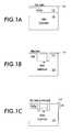
- FIGS. 1A-1Care cross-sectional schematic views illustrating steps used in fabricating a compliant substrate according to an exemplary embodiment of the processes of this invention
- FIG. 2is a plan view of an exemplary embodiment of a compliant substrate according to this invention.
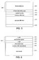
- FIG. 3illustrates an exemplary embodiment of a semiconductor structure according to this invention including one or more lattice mismatched single crystal layers formed on the compliant substrate of FIG. 1C;
- FIG. 4illustrates an exemplary embodiment of a semiconductor structure including a p-i-n photodetector grown on a compliant substrate according to this invention
- FIG. 5illustrates an exemplary embodiment of a semiconductor structure including a long-wavelength semiconductor light-emitting device grown on a compliant substrate according to this invention.
- FIG. 6illustrates an exemplary embodiment of a semiconductor structure including a short-wavelength semiconductor light-emitting device grown on a compliant substrate according to this invention.
- Exemplary embodiments of the compliant substrates according to this inventioninclude a first single crystal layer; an amorphous buffer layer on the first single crystal layer; and a compliant second single crystal layer on the amorphous buffer layer.
- the first single crystal layercan be composed of an element or, alternatively, from a compound or alloy formed from two or more different elements.
- the first single crystal layercan comprise any suitable material, including, but not limited to, GaAs, Si, InP and the like. In embodiments in which the compliant substrate is to be used to grow GaN, GaAs is the preferred material of the first single crystal layer.
- the first single crystal layercan have any desirable thickness, depending on the intended use of the compliant substrate.
- the first single crystal layercan typically have a thickness between about 50 ⁇ m and 2 mm.
- the amorphous buffer layercan comprise an oxidized epitaxial layer.
- the amorphous buffer layercan comprise oxidized AlAs, oxidized AlGaAs, oxidized AlInP and oxidized AlAsSb.
- the amorphous buffer layercan comprise any suitable oxidized material that is sufficiently lattice matched to both the first and second single crystal layers. Suitable exemplary materials for forming the amorphous buffer layer that meet these criteria include, but are not limited to, AlAs, AlGaAs, AlGaAsSb and AlGaInP.
- the buffer layermust have a sufficient thickness (typically at least several nanometers) in order to form a continuous layer. There is no particular upper limit on the thickness of the amorphous buffer layer.
- the amorphous buffer layercan typically have a thickness of from about 20 nm to about 1000 nm.
- the second single crystal layercan be composed of an element or, alternatively, from a compound or alloy formed from two or more elements.
- the second single crystal layercan be a III-V compound semiconductor.
- III-V compoundrefers to compounds and alloys formed from at least one element from Group III of the periodic table and at least one element from Group V of the periodic table.
- Exemplary suitable III-V compoundsinclude, for example, GaAs, InGaAs and GaInP.
- GaAsis the preferred material of the second single crystal layer.
- the second single crystal layerpreferably must be thick enough to provide sufficient coverage of the amorphous buffer layer.
- the second single crystal layerforms a continuous layer on the amorphous buffer layer so that the entire bottom surface of the second single crystal layer contacts with, and is fully supported by, the amorphous buffer layer.
- the second single crystal layeralso preferably must be thin enough to comply or stretch in response to stress being imparted to it by a film being deposited on the second single crystal layer.
- the second single crystal layeris no thicker than a desired thickness, which is related to the “critical thickness” of the second single crystal layer.
- the “critical thickness” of the second single crystal layeris the thickness below which the energy associated with strain in the second single crystal layer is sufficiently low that it does not force defects into a layer grown epitaxially on the second single crystal layer.
- the energy required to deform or to generate defects in the second single crystal layeris less than the energy required to form defects in the epitaxial layer grown on the second single crystal layer. Consequently, defects that may be generated grow downward and not upward into the epitaxially grown layer on the second single crystal layer.
- the critical thickness of the second single crystal layerdepends on the magnitude of the lattice mismatch between the second single crystal layer and the epitaxial layer grown on the second single crystal layer.
- the maximum permissible thickness of the second single crystal layersvaries depending on the composition of the second single crystal layer, the composition of the epitaxial layer grown on it, and the corresponding magnitude of the lattice mismatch between the second single crystal layer and the epitaxial layer.
- This maximum permissible thicknessdecreases with increasing lattice mismatch because the strain energy increases faster with layer thickness for larger lattice mismatch.
- the maximum permissible thicknessalso depends on the growth conditions of the lattice mismatched epitaxial layer. Lower growth temperatures and higher growth rates relax the maximum thickness requirement and allow a thicker second crystal layer. A lower temperature is favorable because it slows the multiplication of dislocations during growth, while faster growth reduces the time needed to grow the epitaxial layer.
- a calculated relationship between the maximum permissible thickness of the second crystal layer and the lattice mismatchcan be found in C. L. Chua, et.
- the second single crystal layerhas a thickness, t, that is no greater than the critical thickness, t crit , (i.e., t ⁇ t crit ).
- tcritical thickness
- the second single crystal layercan be expected to comply or stretch in response to stress being imparted to it by a film deposited on it.
- the second single crystal layercan have a thickness, t, up to about fifteen times the critical thickness, t crit , (i.e., t ⁇ 15 t crit ).
- tcritical thickness
- Such embodimentsprovide a higher thickness tolerance, which can simplify the process of forming the compliant substrates.
- the GaAs layershould preferably have a thickness between about 2 nm and about 20 nm.
- the GaAs layercan have a thickness of up to about 300 nm.
- the present inventionis not limited to these thicknesses, and other thicknesses can be used, if desired.
- this inventionalso provides processes for forming the above-described compliant substrates that comprise an amorphous buffer layer disposed between the first and second single crystal layers.
- Exemplary embodiments of the processes according to this inventioninclude providing a first single crystal layer; forming an intermediate single crystal layer on the first single crystal layer; forming a second single crystal layer on the intermediate single crystal layer; and forming an amorphous buffer layer from the intermediate single crystal layer.
- the second single crystal layershould preferably have a thickness, t, that is no greater than fifteen times the critical thickness, t crit , (i.e., t ⁇ 15 t crit ).
- the thickness of the second single crystal layeris no greater than the critical thickness for reducing, or even substantially preventing, defect formation in epitaxial films grown on the second single crystal layer.
- the amorphous buffer layercan be formed from the intermediate single crystal layer by first forming a trench (i.e., trenching) through the second single crystal layer and exposing the intermediate single crystal layer. After the trench is formed, the intermediate single crystal layer can be oxidized to form the amorphous buffer layer.
- a trenchi.e., trenching
- the intermediate single crystal layercan be converted to amorphous material using any suitable process.
- the intermediate single crystal layeris oxidixed by exposing it to any suitable oxygen-containing gas in an oxidation process.
- the oxygen-containing gascan be a nitrogen gas bubbled through heated water or steam.
- suitable exemplary processes for oxidizing the intermediate single crystal layerinclude, for example, dry O 2 oxidation and anodic oxidation.
- steam in flowing nitrogencan be used as the oxygen-containing gas for oxidizing AlAs single crystal layers.
- An ambient temperatureof from about 380° C. to about 550°C. can typically be used to oxidize the AlAs and form an amorphous buffer layer.
- the oxidation rate of AlAs in steamvaries depending upon the ambient temperature and the composition of the AlAs. The oxidation rate increases with increasing temperature. For example, the presence of small amounts of gallium in the aluminum arsenide tends to inhibit the oxidation. That is, for Al x Ga 1 ⁇ x As, (where x is from 0 to 1), as x increases and the aluminum content accordingly increases, the oxidation rate of the Al x ,Ga 1 ⁇ x As increases.
- GaN-based devicesare currently fabricated on III-V films grown on substrates such as sapphire and SiC. These substrates have a large lattice mismatch with GaN. Consequently, films with low defect densities are difficult to grow and devices that are produced on these substrates exhibit poor performance.
- GaAs substratessuch as shown in FIGS. 1A-1C, are attractive because, unlike sapphire, they can be readily cleaved along certain crystal orientations to form laser facets.
- GaAs substratescan be easily etched using standard chemical etching techniques, thereby increasing process flexibility.
- compliant substrates formed on GaAs wafers in accordance with this inventioncan be more easily processed than can conventional substrates for GaN-based devices.
- FIG. 1Ashows an AlAs intermediate single crystal layer 12 on a GaAs wafer substrate, which forms a first single crystal layer 10 .
- a thin GaAs second single crystal layer 14is formed on top of the AlAs intermediate single crystal layer 12 .
- the GaAs second single crystal layer 14forms a continuous layer on the AlAs intermediate single crystal layer 12 .
- Both the AlAs intermediate single crystal layer 12 and the thin GaAs second single crystal layer 14are first grown on the GaAs first single crystal layer 10 by any suitable epitaxial deposition technique.
- the AlAs intermediate single crystal layer 12 and the thin GaAs second single crystal layer 14can be grown on the GaAs first single crystal layer 10 by metal organic chemical vapor deposition (MOCVD), molecular beam epitaxy (MBE), or any other suitable method.
- MOCVDmetal organic chemical vapor deposition
- MBEmolecular beam epitaxy
- trenches 16can be formed through the thin GaAs second crystal layer 14 to expose the AlAs intermediate single crystal layer 12 .
- the trenches 16can be formed, for example, by patterning narrow openings in photoresist on the surface of the thin GaAs second single crystal layer 14 , so that portions of the thin GaAs second single crystal layer 14 are not covered by resist, and then etching through the thin GaAs second single crystal layer 14 to the AlAs intermediate single crystal layer 12 using any suitable etching technique.
- RIEreactive ion etching
- the AlAs intermediate single crystal buffer layer 12is selectively wet oxidized in the lateral direction until it is completely converted into an amorphous buffer layer 20 .
- the amorphous buffer layer 20 formed by treating the AlAs intermediate single crystal layer 12comprises aluminum oxide (Al x O y ). This oxidation process partially “releases” the thin GaAs second single crystal layer 14 from the amorphous buffer layer 20 , so that these layers are only weakly bonded to each other. As a result of the oxidation process, the GaAs second single crystal layer 14 has the mechanical flexibility that is characteristic of compliant substrates.
- optimization of the adhesion properties of the thin GaAs second single crystal layer 14 to the amorphous buffer layer 20can be accomplished by appropriately grading the composition of an intermediate single crystal layer 12 comprising Al x ,Ga 1 ⁇ x As and the thin GaAs second single crystal layer 14 prior to oxidizing the intermediate single crystal layer 12 to form the amorphous structure of the amorphous buffer layer 20 .
- the aluminum content, xcan be varied typically between 1 and about 0.8 at different distances from the second single crystal layer 14 .
- FIG. 2shows a plan view of the wafer formed by the exemplary process shown in FIGS. 1A-1C. Intersecting trenches 16 separate mesas 18 from each other. Each mesa 18 includes a partially “released” thin GaAs second single crystal layer 14 forming a surface layer.
- the thin GaAs second single crystal layer 14is partially “released” from the underlying amorphous buffer layer 20 , one or more lattice mismatched films can be grown on the thin GaAs second single crystal layer 14 . Because the partially released thin GaAs second single crystal layer 14 has a certain thickness, this layer can comply, or deform, under an epitaxial film grown on the GaAs single crystal layer, so as to match the lattice parameter of the overlying epitaxial film. The deformation of the thin GaAs second single crystal layer 14 minimizes the creation of defects in the overlying epitaxial film, resulting in high-quality epitaxial film material.
- the weak bonding between the amorphous buffer layer 20 and the second single crystal layer 14 of the compliant substratesenables layers of materials that are not lattice matched to the second single crystal layer 14 material (i.e., lattice mismatched layers) to be formed on the compliant substrates.
- lattice mismatched layersAs these lattice mismatched layers grow, the second single crystal layer 14 can deform and allow any defects (dislocations) that may be generated to grow downward and not upward into the lattice mismatched layers. Consequently, high-quality epitaxial films composed of certain materials can be successfully grown on the compliant substrates of this invention, where these same films previously could not be successfully grown on substrates formed from the same materials as the compliant substrates.
- the compliant substrates of this inventionto deform as necessary to accommodate the magnitude of the lattice mismatch between the compliant layers and layers formed on the compliant substrates allows these epitaxial films, and thus also semiconductor structures including the epitaxial films, to be formed on the compliant substrates.
- lattice mismatched layers of increased thicknesscan be grown on the compliant substrates according to this invention, due to the ability of the compliant layers to deform during the growth of the lattice mismatched films.
- the thicker layerscan improve the performance of various electronic and optoelectronic devices as described below.
- the compliant substrates according to this inventioncan be used as templates for the growth of epitaxial films and semiconductor structures that could not previously be successfully formed on the same materials that can form the compliant substrates, and also that include layers that are thicker than those that could previously be grown on substrates.
- this inventionprovides semiconductor structures formed on the compliant substrates.
- the semiconductor structuresinclude one or more substantially lattice mismatched single crystal layers formed on the second single crystal layer 14 (compliant layer) of the compliant substrate.
- Exemplary lattice mismatched film compositionsthat can be grown on the compliant layers of the compliant substrates of this invention include, for example, but are not limited to, InAlGaAsN, InAlGaAsP, InAlGaAsSb and the like.
- the amount of each Group III or Group V element, relative to other Group III or Group V elements in the respective compoundcan range from 0% to 100%.
- FIG. 3illustrates an exemplary semiconductor structures 30 formed on the compliant substrate shown in FIG. 1 C.
- the semiconductor structure 30includes at least one lattice mismatched layer 32 formed on the second single crystal layer 14 of the compliant substrate.
- the semiconductor substratescan comprise various electronic and optoelectronic devices including, for example, photodetectors, multiple quantum well optical modulators, semiconductor lasers, transistors and light emitting diodes (LEDs).
- highly-strained p-i-n photodetectorscomprising an intrinsic semiconductor layer sandwiched between an n-type semiconductor layer and a p-type semiconductor layer can be formed on the compliant substrates of this invention.
- FIG. 4shows an exemplary highly-strained p-i-n photodetector 130 comprising an intrinsic In, 0.14 Ga 0.86 As layer 142 sandwiched between an n-type In 0.14 Ga 0.86 As layer 140 formed on a GaAs compliant layer 114 of the compliant substrate, and a p-type In 0.14 Ga 0.86 As layer 144 .
- Other material compositions for the layers of the p-i-n photodetector 130can also be used.
- the p-i-n photodetectorscan comprise thick layers of strained absorbing material. Such photodetectors containing thick strained layers could not previously be grown above a certain thickness without inducing substantial crystal defects. A thick absorbing region is essential for providing good photodetector sensitivity, which is desirable because it produces a large signal for a given detected light intensity.
- the n-type In 0.14 Ga 0.86 As layer 140 , the intrinsic In 0.14 Ga 0.86 As layer 142 , and the p-type In 0.14 Ga 0.86 As layer 144can each be about 1 ⁇ m thick.
- the composite structurecan comprise a 1% strained photodetector on GaAs.
- the compliant substrates of this inventioncan also be used as substrates for growing long-wavelength semiconductor light-emitting devices, such as long-wavelength semiconductor lasers and light-emitting diodes.
- semiconductor light-emitting devicesemit at a wavelength of from about 1.1 ⁇ m to about 2 ⁇ m.
- InP-based long-wavelength semiconductor laserscan be grown on GaAs compliant substrates according to this invention.
- InP-based laser materials on GaAs compliant substratesprovides increased flexibility in the device structures because GaAs-based epi layers, that are not normally available to InP-based systems, can be incorporated in the structures.
- long-wavelength, vertical-cavity, surface-emitting lasersrequire a low bandgap light-emitting material.
- Such materialscan be realized using InP-based epi-layers.
- these lasersalso need a highly reflective mirror that is very difficult to form using InP-based materials.
- the InP-based light-emitting regioncan be integrated with GaAs-based mirrors, which have a higher reflectivity and a wider reflectivity bandwidth than their InP-based counterparts.
- the semiconductor structurecomprises a GaAs-based distributed bragg reflector (DBR) mirror 215 grown on a GaAs substrate 210 and typically includes about thirty-five pairs of quarter-wavelength thick alternating layers of AlAs/GaAs.
- An InP-based light-emitting region 250is formed on a compliant GaAs layer 214 .
- the InP-based light-emitting regionincludes an InGaAsP multiple quantum well region including material compositions that can emit light at a wavelength of 1.55 microns.
- a dielectric DBR mirror 252is formed on the InP-based light-emitting region 250 .
- the dielectric DBR mirror 252typically comprises four pairs of quarter-wavelength thick alternating layers of Si/SiO 2 , which can be formed by any suitable process such as electron-beam evaporation.
- short-wavelength semiconductor light-emitting devicesincluding lasers and light-emitting diodes. These light-emitting devices emit at a wavelength of less than about 600 nm and include yellow light emitting devices (i.e., devices emitting at a wavelength of from about 570-590 nm) and blue light emitting devices (i.e., lasers and LEDs emitting at a wavelength of from about 450-490 nm).
- Short-wavelength semiconductor light-emitting devices including thick, highly strained epitaxial filmscan be grown on compliant substrates according to this invention.
- GaNcan be grown on the compliant substrates of this invention.
- the thin GaAs second single crystal layer 14can minimize the creation of defects in such expitaxial GaN films, resulting in the formation of high-quality GaN material.
- Low-defect GaNis particularly well suited for fabricating high-quality light emitting devices that emit blue light.
- FIG. 6An exemplary embodiment of a semiconductor structure including a semiconductor short-wavelength light-emitting device 330 including GaN-based epitaxial layers is shown in FIG. 6 .
- the light-emitting device 330comprises an n-GaN layer 360 grown on a GaAs compliant layer 314 of a compliant substrate, an InGaN multiple quantum well region 362 formed on the n-GaN layer 360 , and a p-GaN layer 364 formed on the InGaN multiple quantum well region 362 .
- the compliant substrates of this inventioncan also be used in optoelectronic integration applications.
- GaN devicescan be formed on GaAs containing GaAs-based devices to make multiple-wavelength emitting light sources.
- Such multiple-wavelength light sourcescan be used, for example, in high speed printing where each wavelength encodes a separate data stream.
- InP-based devicescan also be integrated with GaAs-based transistors using the compliant substrates of this invention, providing increased device design flexibility.
- this inventionprovides compliant substrates that include single crystal layers that are compliant and able to mechanically deform, or comply, to match the lattice parameter of epitaxial films grown on them.
- the compliant substratescan be formed from various materials, including III-V compound materials, using conventional processing techniques.
- the compliant substratescan be used as templates for the growth of various semiconductor structures that include lattice mismatched layers that previously have not been successfully grown on substrates.
Landscapes
- Engineering & Computer Science (AREA)
- Microelectronics & Electronic Packaging (AREA)
- Computer Hardware Design (AREA)
- Power Engineering (AREA)
- Condensed Matter Physics & Semiconductors (AREA)
- General Physics & Mathematics (AREA)
- Manufacturing & Machinery (AREA)
- Physics & Mathematics (AREA)
- Chemical & Material Sciences (AREA)
- Crystallography & Structural Chemistry (AREA)
- Materials Engineering (AREA)
- General Chemical & Material Sciences (AREA)
- Chemical Kinetics & Catalysis (AREA)
- Metallurgy (AREA)
- Organic Chemistry (AREA)
- Recrystallisation Techniques (AREA)
Abstract
Description
Claims (43)
Priority Applications (1)
| Application Number | Priority Date | Filing Date | Title |
|---|---|---|---|
| US09/559,828US6372356B1 (en) | 1998-06-04 | 2000-04-28 | Compliant substrates for growing lattice mismatched films |
Applications Claiming Priority (2)
| Application Number | Priority Date | Filing Date | Title |
|---|---|---|---|
| US9034498A | 1998-06-04 | 1998-06-04 | |
| US09/559,828US6372356B1 (en) | 1998-06-04 | 2000-04-28 | Compliant substrates for growing lattice mismatched films |
Related Parent Applications (1)
| Application Number | Title | Priority Date | Filing Date |
|---|---|---|---|
| US9034498AContinuation-In-Part | 1998-06-04 | 1998-06-04 |
Publications (1)
| Publication Number | Publication Date |
|---|---|
| US6372356B1true US6372356B1 (en) | 2002-04-16 |
Family
ID=22222382
Family Applications (1)
| Application Number | Title | Priority Date | Filing Date |
|---|---|---|---|
| US09/559,828Expired - LifetimeUS6372356B1 (en) | 1998-06-04 | 2000-04-28 | Compliant substrates for growing lattice mismatched films |
Country Status (1)
| Country | Link |
|---|---|
| US (1) | US6372356B1 (en) |
Cited By (71)
| Publication number | Priority date | Publication date | Assignee | Title |
|---|---|---|---|---|
| US20010054717A1 (en)* | 2000-06-22 | 2001-12-27 | Showa Denko K.K | Group-III nitride semiconductor light-emitting device and production method thereof |
| US20020084000A1 (en)* | 1997-06-24 | 2002-07-04 | Eugene A. Fitzgerald | Controlling threading dislocation densities in Ge on Si using graded GeSi layers and planarization |
| US20020167070A1 (en)* | 2000-06-30 | 2002-11-14 | Motorola, Inc. | Hybrid semiconductor structure and device |
| US20030034529A1 (en)* | 2000-12-04 | 2003-02-20 | Amberwave Systems Corporation | CMOS inverter and integrated circuits utilizing strained silicon surface channel MOSFETs |
| US20030077867A1 (en)* | 2001-03-02 | 2003-04-24 | Fitzergald Eugene A. | Relaxed silicon germanium platform for high speed CMOS electronics and high speed analog circuits |
| US6555946B1 (en) | 2000-07-24 | 2003-04-29 | Motorola, Inc. | Acoustic wave device and process for forming the same |
| US6573126B2 (en) | 2000-08-16 | 2003-06-03 | Massachusetts Institute Of Technology | Process for producing semiconductor article using graded epitaxial growth |
| US20030102498A1 (en)* | 2001-09-24 | 2003-06-05 | Glyn Braithwaite | RF circuits including transistors having strained material layers |
| US6576113B1 (en)* | 1999-10-29 | 2003-06-10 | California Institute Of Technology | Method of electroplating of high aspect ratio metal structures into semiconductors |
| US20030113948A1 (en)* | 2000-01-20 | 2003-06-19 | Amberwave Systems Corporation | Low threading dislocation density relaxed mismatched epilayers without high temperature growth |
| US6589856B2 (en) | 2001-08-06 | 2003-07-08 | Motorola, Inc. | Method and apparatus for controlling anti-phase domains in semiconductor structures and devices |
| US6602613B1 (en)* | 2000-01-20 | 2003-08-05 | Amberwave Systems Corporation | Heterointegration of materials using deposition and bonding |
| US6639249B2 (en) | 2001-08-06 | 2003-10-28 | Motorola, Inc. | Structure and method for fabrication for a solid-state lighting device |
| US6638838B1 (en) | 2000-10-02 | 2003-10-28 | Motorola, Inc. | Semiconductor structure including a partially annealed layer and method of forming the same |
| US20030207589A1 (en)* | 2002-05-03 | 2003-11-06 | Thoughtbeam, Inc. | Method for growing a monocrystalline oxide layer and for fabricating a semiconductor device on a monocrystalline substrate |
| US6646293B2 (en) | 2001-07-18 | 2003-11-11 | Motorola, Inc. | Structure for fabricating high electron mobility transistors utilizing the formation of complaint substrates |
| US6649480B2 (en) | 2000-12-04 | 2003-11-18 | Amberwave Systems Corporation | Method of fabricating CMOS inverter and integrated circuits utilizing strained silicon surface channel MOSFETs |
| US20030213950A1 (en)* | 2000-05-31 | 2003-11-20 | Applied Optoelectronics, Inc. | Alternative substrates for epitaxial growth |
| US20030227029A1 (en)* | 2002-06-07 | 2003-12-11 | Amberwave Systems Corporation | Elevated source and drain elements for strained-channel heterojuntion field-effect transistors |
| US20030227057A1 (en)* | 2002-06-07 | 2003-12-11 | Lochtefeld Anthony J. | Strained-semiconductor-on-insulator device structures |
| US6667196B2 (en) | 2001-07-25 | 2003-12-23 | Motorola, Inc. | Method for real-time monitoring and controlling perovskite oxide film growth and semiconductor structure formed using the method |
| US20040000268A1 (en)* | 1998-04-10 | 2004-01-01 | Massachusetts Institute Of Technology | Etch stop layer system |
| US6673646B2 (en) | 2001-02-28 | 2004-01-06 | Motorola, Inc. | Growth of compound semiconductor structures on patterned oxide films and process for fabricating same |
| US6673667B2 (en) | 2001-08-15 | 2004-01-06 | Motorola, Inc. | Method for manufacturing a substantially integral monolithic apparatus including a plurality of semiconductor materials |
| US20040005740A1 (en)* | 2002-06-07 | 2004-01-08 | Amberwave Systems Corporation | Strained-semiconductor-on-insulator device structures |
| US6693298B2 (en) | 2001-07-20 | 2004-02-17 | Motorola, Inc. | Structure and method for fabricating epitaxial semiconductor on insulator (SOI) structures and devices utilizing the formation of a compliant substrate for materials used to form same |
| US6693033B2 (en) | 2000-02-10 | 2004-02-17 | Motorola, Inc. | Method of removing an amorphous oxide from a monocrystalline surface |
| US20040031979A1 (en)* | 2002-06-07 | 2004-02-19 | Amberwave Systems Corporation | Strained-semiconductor-on-insulator device structures |
| US20040043548A1 (en)* | 2002-08-27 | 2004-03-04 | Redd Randy D. | Method for forming a semiconductor device |
| US20040040493A1 (en)* | 2002-08-30 | 2004-03-04 | Amberwave Systems Corporation | Reduction of dislocation pile-up formation during relaxed lattice-mismatched epitaxy |
| US6703688B1 (en) | 2001-03-02 | 2004-03-09 | Amberwave Systems Corporation | Relaxed silicon germanium platform for high speed CMOS electronics and high speed analog circuits |
| US6709989B2 (en) | 2001-06-21 | 2004-03-23 | Motorola, Inc. | Method for fabricating a semiconductor structure including a metal oxide interface with silicon |
| US6724008B2 (en) | 2001-03-02 | 2004-04-20 | Amberwave Systems Corporation | Relaxed silicon germanium platform for high speed CMOS electronics and high speed analog circuits |
| US20040075105A1 (en)* | 2002-08-23 | 2004-04-22 | Amberwave Systems Corporation | Semiconductor heterostructures having reduced dislocation pile-ups and related methods |
| US6750130B1 (en) | 2000-01-20 | 2004-06-15 | Amberwave Systems Corporation | Heterointegration of materials using deposition and bonding |
| US6855992B2 (en) | 2001-07-24 | 2005-02-15 | Motorola Inc. | Structure and method for fabricating configurable transistor devices utilizing the formation of a compliant substrate for materials used to form the same |
| US20050042849A1 (en)* | 2002-06-25 | 2005-02-24 | Amberwave Systems Corporation | Reacted conductive gate electrodes |
| US20050054168A1 (en)* | 2001-09-21 | 2005-03-10 | Amberwave Systems Corporation | Semiconductor structures employing strained material layers with defined impurity gradients and methods for fabricating same |
| US6885065B2 (en) | 2002-11-20 | 2005-04-26 | Freescale Semiconductor, Inc. | Ferromagnetic semiconductor structure and method for forming the same |
| US20050176204A1 (en)* | 2002-06-10 | 2005-08-11 | Amberwave Systems Corporation | Source and drain elements |
| US6940089B2 (en) | 2001-04-04 | 2005-09-06 | Massachusetts Institute Of Technology | Semiconductor device structure |
| US20050195012A1 (en)* | 2004-03-02 | 2005-09-08 | Atsushi Sueoka | Semiconductor device |
| US6965128B2 (en) | 2003-02-03 | 2005-11-15 | Freescale Semiconductor, Inc. | Structure and method for fabricating semiconductor microresonator devices |
| US20060014366A1 (en)* | 2002-06-07 | 2006-01-19 | Amberwave Systems Corporation | Control of strain in device layers by prevention of relaxation |
| US20060011984A1 (en)* | 2002-06-07 | 2006-01-19 | Amberwave Systems Corporation | Control of strain in device layers by selective relaxation |
| US6992321B2 (en) | 2001-07-13 | 2006-01-31 | Motorola, Inc. | Structure and method for fabricating semiconductor structures and devices utilizing piezoelectric materials |
| US7005717B2 (en) | 2000-05-31 | 2006-02-28 | Freescale Semiconductor, Inc. | Semiconductor device and method |
| US7019332B2 (en) | 2001-07-20 | 2006-03-28 | Freescale Semiconductor, Inc. | Fabrication of a wavelength locker within a semiconductor structure |
| US7020374B2 (en) | 2003-02-03 | 2006-03-28 | Freescale Semiconductor, Inc. | Optical waveguide structure and method for fabricating the same |
| US7045815B2 (en) | 2001-04-02 | 2006-05-16 | Freescale Semiconductor, Inc. | Semiconductor structure exhibiting reduced leakage current and method of fabricating same |
| US7060632B2 (en) | 2002-03-14 | 2006-06-13 | Amberwave Systems Corporation | Methods for fabricating strained layers on semiconductor substrates |
| US7067856B2 (en) | 2000-02-10 | 2006-06-27 | Freescale Semiconductor, Inc. | Semiconductor structure, semiconductor device, communicating device, integrated circuit, and process for fabricating the same |
| US20060172505A1 (en)* | 2005-01-31 | 2006-08-03 | Koester Steven J | Structure and method of integrating compound and elemental semiconductors for high-performace CMOS |
| US7105866B2 (en) | 2000-07-24 | 2006-09-12 | Freescale Semiconductor, Inc. | Heterojunction tunneling diodes and process for fabricating same |
| US20060246267A1 (en)* | 2005-04-08 | 2006-11-02 | Versatilis Llc | System and method for manufacturing thick and thin film devices using a donee layer cleaved from a crystalline donor |
| US7161227B2 (en) | 2001-08-14 | 2007-01-09 | Motorola, Inc. | Structure and method for fabricating semiconductor structures and devices for detecting an object |
| US7169619B2 (en) | 2002-11-19 | 2007-01-30 | Freescale Semiconductor, Inc. | Method for fabricating semiconductor structures on vicinal substrates using a low temperature, low pressure, alkaline earth metal-rich process |
| US7211852B2 (en) | 2001-01-19 | 2007-05-01 | Freescale Semiconductor, Inc. | Structure and method for fabricating GaN devices utilizing the formation of a compliant substrate |
| US7332417B2 (en) | 2003-01-27 | 2008-02-19 | Amberwave Systems Corporation | Semiconductor structures with structural homogeneity |
| US7342276B2 (en) | 2001-10-17 | 2008-03-11 | Freescale Semiconductor, Inc. | Method and apparatus utilizing monocrystalline insulator |
| US7393733B2 (en) | 2004-12-01 | 2008-07-01 | Amberwave Systems Corporation | Methods of forming hybrid fin field-effect transistor structures |
| US20080179636A1 (en)* | 2007-01-27 | 2008-07-31 | International Business Machines Corporation | N-fets with tensilely strained semiconductor channels, and method for fabricating same using buried pseudomorphic layers |
| US7504704B2 (en) | 2003-03-07 | 2009-03-17 | Amberwave Systems Corporation | Shallow trench isolation process |
| US20100254425A1 (en)* | 2007-06-29 | 2010-10-07 | International Business Machines Corporation | Phase change material based temperature sensor |
| US8822282B2 (en) | 2001-03-02 | 2014-09-02 | Taiwan Semiconductor Manufacturing Company, Ltd. | Methods of fabricating contact regions for FET incorporating SiGe |
| TWI506675B (en)* | 2007-12-28 | 2015-11-01 | Sumitomo Chemical Co | Semiconductor substrate, method of manufacturing semiconductor substrate, and electronic device |
| US9818872B2 (en)* | 2015-06-30 | 2017-11-14 | Taiwan Semiconductor Manufacturing Company, Ltd. | Multi-gate device and method of fabrication thereof |
| US9853107B2 (en)* | 2014-03-28 | 2017-12-26 | Intel Corporation | Selective epitaxially grown III-V materials based devices |
| CN107785238A (en)* | 2016-08-25 | 2018-03-09 | 西安电子科技大学 | InGaAs materials, based on the MOS device of InGaAs materials as raceway groove and preparation method thereof |
| US20180277368A1 (en)* | 2017-03-23 | 2018-09-27 | International Business Machines Corporation | Post growth heteroepitaxial layer separation for defect reduction in heteroepitaxial films |
| US10217900B2 (en)* | 2017-07-06 | 2019-02-26 | Globalfoundries Inc. | Light emitting diode structures |
Citations (14)
| Publication number | Priority date | Publication date | Assignee | Title |
|---|---|---|---|---|
| US4876219A (en)* | 1988-03-04 | 1989-10-24 | Fujitsu Limited | Method of forming a heteroepitaxial semiconductor thin film using amorphous buffer layers |
| US5300320A (en) | 1992-06-23 | 1994-04-05 | President And Fellows Of Harvard College | Chemical vapor deposition from single organometallic precursors |
| US5486857A (en) | 1989-08-15 | 1996-01-23 | Minnesota Mining And Manufacturing Company | Thermal imaging system |
| US5498595A (en) | 1988-07-02 | 1996-03-12 | British Technology Group Limited | Method of activation of superconductors and devices produced thereby |
| US5506420A (en) | 1994-09-14 | 1996-04-09 | The Regents Of The University Of California | Semiconductor bio-electronic devices incorporating biochemical stabilization layers |
| US5617446A (en)* | 1994-07-11 | 1997-04-01 | Sony Corporation | Surface-emitting semiconductor light emitting device |
| US5633516A (en)* | 1994-07-25 | 1997-05-27 | Hitachi, Ltd. | Lattice-mismatched crystal structures and semiconductor device using the same |
| US5661112A (en) | 1987-07-24 | 1997-08-26 | Hatta; Shinichiro | Superconductor |
| US5780163A (en) | 1996-06-05 | 1998-07-14 | Dow Corning Corporation | Multilayer coating for microelectronic devices |
| US5824418A (en) | 1995-09-05 | 1998-10-20 | Northrop Grumman Corporation | Optically transparent, electrically conductive semiconductor windows |
| US5841156A (en)* | 1996-10-11 | 1998-11-24 | Mitsubishi Denki Kabushiki Kaisha | Semiconductor device including T1 GaAs layer |
| US5883911A (en)* | 1995-12-20 | 1999-03-16 | Electronics And Telecommunications Research Institute | Surface-emitting laser device |
| US5903017A (en)* | 1996-02-26 | 1999-05-11 | Kabushiki Kaisha Toshiba | Compound semiconductor device formed of nitrogen-containing gallium compound such as GaN, AlGaN or InGaN |
| US6072202A (en)* | 1996-09-26 | 2000-06-06 | Nec Corporation | II-VI compound semiconductor device with III-V buffer layer |
- 2000
- 2000-04-28USUS09/559,828patent/US6372356B1/ennot_activeExpired - Lifetime
Patent Citations (14)
| Publication number | Priority date | Publication date | Assignee | Title |
|---|---|---|---|---|
| US5661112A (en) | 1987-07-24 | 1997-08-26 | Hatta; Shinichiro | Superconductor |
| US4876219A (en)* | 1988-03-04 | 1989-10-24 | Fujitsu Limited | Method of forming a heteroepitaxial semiconductor thin film using amorphous buffer layers |
| US5498595A (en) | 1988-07-02 | 1996-03-12 | British Technology Group Limited | Method of activation of superconductors and devices produced thereby |
| US5486857A (en) | 1989-08-15 | 1996-01-23 | Minnesota Mining And Manufacturing Company | Thermal imaging system |
| US5300320A (en) | 1992-06-23 | 1994-04-05 | President And Fellows Of Harvard College | Chemical vapor deposition from single organometallic precursors |
| US5617446A (en)* | 1994-07-11 | 1997-04-01 | Sony Corporation | Surface-emitting semiconductor light emitting device |
| US5633516A (en)* | 1994-07-25 | 1997-05-27 | Hitachi, Ltd. | Lattice-mismatched crystal structures and semiconductor device using the same |
| US5506420A (en) | 1994-09-14 | 1996-04-09 | The Regents Of The University Of California | Semiconductor bio-electronic devices incorporating biochemical stabilization layers |
| US5824418A (en) | 1995-09-05 | 1998-10-20 | Northrop Grumman Corporation | Optically transparent, electrically conductive semiconductor windows |
| US5883911A (en)* | 1995-12-20 | 1999-03-16 | Electronics And Telecommunications Research Institute | Surface-emitting laser device |
| US5903017A (en)* | 1996-02-26 | 1999-05-11 | Kabushiki Kaisha Toshiba | Compound semiconductor device formed of nitrogen-containing gallium compound such as GaN, AlGaN or InGaN |
| US5780163A (en) | 1996-06-05 | 1998-07-14 | Dow Corning Corporation | Multilayer coating for microelectronic devices |
| US6072202A (en)* | 1996-09-26 | 2000-06-06 | Nec Corporation | II-VI compound semiconductor device with III-V buffer layer |
| US5841156A (en)* | 1996-10-11 | 1998-11-24 | Mitsubishi Denki Kabushiki Kaisha | Semiconductor device including T1 GaAs layer |
Non-Patent Citations (6)
| Title |
|---|
| A. Black, A.R. Hawkins, N.M. Margalit, D.I. Babic, A.L. Holmes, Jr., Y.L. Chang, P. Abrahams, J.E. Bowers, and E.L. Hu, "Wafer Fusion: Materials Issues and Device Results," IEEE Journal of Selected Topics in Quantum Electronics, vol. 3, No. 3, pp. 943-951, 1997. |
| A.R. Powell, S.S. Iyer and F.K. LeGoues, "New Approach to the Growth of Low Dislocation Relaxed SiGe Material", Appl. Phys. Lett. 64 (14), pp. 1856-1858, 1994. |
| C.L. Chua, W.Y. Hsu, F. Ejeckam, A. Tran, and Y.H. Lo, "Growing Pseudomorphic Layers Beyond the Critical Thickness Using Free-Standing Compliant Substrates," Mat. Res. Soc. Symp. Proc. vol. 326, pp. 21-26, 1994. |
| C.L. Chura, W.Y. Hsu, C.H. Lin, G. Christenson, and Y.H. Lo, "Overcoming the pseudomorphic critical thickness limit using compliant substrates," Appl. Phys. Lett., vol. 64 (26), pp. 3640-3642, 1994. |
| F.E. Ejeckam, Y. Qian, Z.H. Zhu, Y.H. Lo, S. Subramanian, and S.L. Sass, "Misaligned (or twist) wafer-bonding: a new technology for making III-V compliant substrates," LEOS '96, Boston, MA, paper ThK2, 1996, pp. 352-353. |
| L.B. Freund and W.D. Nix, "A critical thickness condition for a strained compliant substrate/epitaxial film system," Appl. Phys. Lett., vol. 69 (2), pp. 173-175, 1996. |
Cited By (139)
| Publication number | Priority date | Publication date | Assignee | Title |
|---|---|---|---|---|
| US20020084000A1 (en)* | 1997-06-24 | 2002-07-04 | Eugene A. Fitzgerald | Controlling threading dislocation densities in Ge on Si using graded GeSi layers and planarization |
| US7250359B2 (en) | 1997-06-24 | 2007-07-31 | Massachusetts Institute Of Technology | Controlling threading dislocation densities in Ge on Si using graded GeSi layers and planarization |
| US20040262631A1 (en)* | 1997-06-24 | 2004-12-30 | Massachusetts Institute Of Technology | Controlling threading dislocation densities in Ge on Si using graded GeSi layers and planarization |
| US7081410B2 (en) | 1997-06-24 | 2006-07-25 | Massachusetts Institute Of Technology | Controlling threading dislocation densities in Ge on Si using graded GeSi layers and planarization |
| US6876010B1 (en) | 1997-06-24 | 2005-04-05 | Massachusetts Institute Of Technology | Controlling threading dislocation densities in Ge on Si using graded GeSi layers and planarization |
| US7227176B2 (en) | 1998-04-10 | 2007-06-05 | Massachusetts Institute Of Technology | Etch stop layer system |
| US20040000268A1 (en)* | 1998-04-10 | 2004-01-01 | Massachusetts Institute Of Technology | Etch stop layer system |
| US6576113B1 (en)* | 1999-10-29 | 2003-06-10 | California Institute Of Technology | Method of electroplating of high aspect ratio metal structures into semiconductors |
| US6750130B1 (en) | 2000-01-20 | 2004-06-15 | Amberwave Systems Corporation | Heterointegration of materials using deposition and bonding |
| US20030113948A1 (en)* | 2000-01-20 | 2003-06-19 | Amberwave Systems Corporation | Low threading dislocation density relaxed mismatched epilayers without high temperature growth |
| US6864115B2 (en) | 2000-01-20 | 2005-03-08 | Amberwave Systems Corporation | Low threading dislocation density relaxed mismatched epilayers without high temperature growth |
| US6602613B1 (en)* | 2000-01-20 | 2003-08-05 | Amberwave Systems Corporation | Heterointegration of materials using deposition and bonding |
| US6703144B2 (en) | 2000-01-20 | 2004-03-09 | Amberwave Systems Corporation | Heterointegration of materials using deposition and bonding |
| US6693033B2 (en) | 2000-02-10 | 2004-02-17 | Motorola, Inc. | Method of removing an amorphous oxide from a monocrystalline surface |
| US7067856B2 (en) | 2000-02-10 | 2006-06-27 | Freescale Semiconductor, Inc. | Semiconductor structure, semiconductor device, communicating device, integrated circuit, and process for fabricating the same |
| US6746777B1 (en)* | 2000-05-31 | 2004-06-08 | Applied Optoelectronics, Inc. | Alternative substrates for epitaxial growth |
| US20030213950A1 (en)* | 2000-05-31 | 2003-11-20 | Applied Optoelectronics, Inc. | Alternative substrates for epitaxial growth |
| US7005717B2 (en) | 2000-05-31 | 2006-02-28 | Freescale Semiconductor, Inc. | Semiconductor device and method |
| US6787814B2 (en)* | 2000-06-22 | 2004-09-07 | Showa Denko Kabushiki Kaisha | Group-III nitride semiconductor light-emitting device and production method thereof |
| US20010054717A1 (en)* | 2000-06-22 | 2001-12-27 | Showa Denko K.K | Group-III nitride semiconductor light-emitting device and production method thereof |
| US7211836B2 (en) | 2000-06-22 | 2007-05-01 | Showa Denko Kabushiki Kaisha | Group-III nitride semiconductor light-emitting device and production method thereof |
| US20040144990A1 (en)* | 2000-06-22 | 2004-07-29 | Showa Denko K.K. | Group-III nitride semiconductor light-emitting device and production method thereof |
| US20020167070A1 (en)* | 2000-06-30 | 2002-11-14 | Motorola, Inc. | Hybrid semiconductor structure and device |
| US7105866B2 (en) | 2000-07-24 | 2006-09-12 | Freescale Semiconductor, Inc. | Heterojunction tunneling diodes and process for fabricating same |
| US6555946B1 (en) | 2000-07-24 | 2003-04-29 | Motorola, Inc. | Acoustic wave device and process for forming the same |
| US6573126B2 (en) | 2000-08-16 | 2003-06-03 | Massachusetts Institute Of Technology | Process for producing semiconductor article using graded epitaxial growth |
| US6921914B2 (en) | 2000-08-16 | 2005-07-26 | Massachusetts Institute Of Technology | Process for producing semiconductor article using graded epitaxial growth |
| US20030168654A1 (en)* | 2000-08-16 | 2003-09-11 | Massachusetts Institute Of Technology | Process for producing semiconductor article using graded epitaxial growth |
| US20040173791A1 (en)* | 2000-08-16 | 2004-09-09 | Massachusetts Institute Of Technology | Semiconductor substrate structure |
| US6737670B2 (en) | 2000-08-16 | 2004-05-18 | Massachusetts Institute Of Technology | Semiconductor substrate structure |
| US6713326B2 (en) | 2000-08-16 | 2004-03-30 | Masachusetts Institute Of Technology | Process for producing semiconductor article using graded epitaxial growth |
| US6638838B1 (en) | 2000-10-02 | 2003-10-28 | Motorola, Inc. | Semiconductor structure including a partially annealed layer and method of forming the same |
| US6881632B2 (en) | 2000-12-04 | 2005-04-19 | Amberwave Systems Corporation | Method of fabricating CMOS inverter and integrated circuits utilizing strained surface channel MOSFETS |
| US20030034529A1 (en)* | 2000-12-04 | 2003-02-20 | Amberwave Systems Corporation | CMOS inverter and integrated circuits utilizing strained silicon surface channel MOSFETs |
| US6649480B2 (en) | 2000-12-04 | 2003-11-18 | Amberwave Systems Corporation | Method of fabricating CMOS inverter and integrated circuits utilizing strained silicon surface channel MOSFETs |
| US20040075149A1 (en)* | 2000-12-04 | 2004-04-22 | Amberwave Systems Corporation | CMOS inverter and integrated circuits utilizing strained silicon surface channel MOSFETs |
| US7211852B2 (en) | 2001-01-19 | 2007-05-01 | Freescale Semiconductor, Inc. | Structure and method for fabricating GaN devices utilizing the formation of a compliant substrate |
| US6673646B2 (en) | 2001-02-28 | 2004-01-06 | Motorola, Inc. | Growth of compound semiconductor structures on patterned oxide films and process for fabricating same |
| US7256142B2 (en) | 2001-03-02 | 2007-08-14 | Amberwave Systems Corporation | Relaxed SiGe platform for high speed CMOS electronics and high speed analog circuits |
| US6703688B1 (en) | 2001-03-02 | 2004-03-09 | Amberwave Systems Corporation | Relaxed silicon germanium platform for high speed CMOS electronics and high speed analog circuits |
| US6723661B2 (en) | 2001-03-02 | 2004-04-20 | Amberwave Systems Corporation | Relaxed silicon germanium platform for high speed CMOS electronics and high speed analog circuits |
| US6724008B2 (en) | 2001-03-02 | 2004-04-20 | Amberwave Systems Corporation | Relaxed silicon germanium platform for high speed CMOS electronics and high speed analog circuits |
| US7501351B2 (en) | 2001-03-02 | 2009-03-10 | Amberwave Systems Corporation | Relaxed SiGe platform for high speed CMOS electronics and high speed analog circuits |
| US8822282B2 (en) | 2001-03-02 | 2014-09-02 | Taiwan Semiconductor Manufacturing Company, Ltd. | Methods of fabricating contact regions for FET incorporating SiGe |
| US20030077867A1 (en)* | 2001-03-02 | 2003-04-24 | Fitzergald Eugene A. | Relaxed silicon germanium platform for high speed CMOS electronics and high speed analog circuits |
| US7045815B2 (en) | 2001-04-02 | 2006-05-16 | Freescale Semiconductor, Inc. | Semiconductor structure exhibiting reduced leakage current and method of fabricating same |
| US6940089B2 (en) | 2001-04-04 | 2005-09-06 | Massachusetts Institute Of Technology | Semiconductor device structure |
| US7348259B2 (en) | 2001-04-04 | 2008-03-25 | Massachusetts Institute Of Technology | Method of fabricating a semiconductor structure that includes transferring one or more material layers to a substrate and smoothing an exposed surface of at least one of the material layers |
| US6709989B2 (en) | 2001-06-21 | 2004-03-23 | Motorola, Inc. | Method for fabricating a semiconductor structure including a metal oxide interface with silicon |
| US6992321B2 (en) | 2001-07-13 | 2006-01-31 | Motorola, Inc. | Structure and method for fabricating semiconductor structures and devices utilizing piezoelectric materials |
| US6646293B2 (en) | 2001-07-18 | 2003-11-11 | Motorola, Inc. | Structure for fabricating high electron mobility transistors utilizing the formation of complaint substrates |
| US7019332B2 (en) | 2001-07-20 | 2006-03-28 | Freescale Semiconductor, Inc. | Fabrication of a wavelength locker within a semiconductor structure |
| US6693298B2 (en) | 2001-07-20 | 2004-02-17 | Motorola, Inc. | Structure and method for fabricating epitaxial semiconductor on insulator (SOI) structures and devices utilizing the formation of a compliant substrate for materials used to form same |
| US6855992B2 (en) | 2001-07-24 | 2005-02-15 | Motorola Inc. | Structure and method for fabricating configurable transistor devices utilizing the formation of a compliant substrate for materials used to form the same |
| US6667196B2 (en) | 2001-07-25 | 2003-12-23 | Motorola, Inc. | Method for real-time monitoring and controlling perovskite oxide film growth and semiconductor structure formed using the method |
| US6589856B2 (en) | 2001-08-06 | 2003-07-08 | Motorola, Inc. | Method and apparatus for controlling anti-phase domains in semiconductor structures and devices |
| US6639249B2 (en) | 2001-08-06 | 2003-10-28 | Motorola, Inc. | Structure and method for fabrication for a solid-state lighting device |
| US7161227B2 (en) | 2001-08-14 | 2007-01-09 | Motorola, Inc. | Structure and method for fabricating semiconductor structures and devices for detecting an object |
| US6673667B2 (en) | 2001-08-15 | 2004-01-06 | Motorola, Inc. | Method for manufacturing a substantially integral monolithic apparatus including a plurality of semiconductor materials |
| US7884353B2 (en) | 2001-09-21 | 2011-02-08 | Taiwan Semiconductor Manufacturing Company, Ltd. | Semiconductor structures employing strained material layers with defined impurity gradients and methods for fabricating same |
| US20070293003A1 (en)* | 2001-09-21 | 2007-12-20 | Matthew Currie | Semiconductor structures employing strained material layers with defined impurity gradients and methods for fabricating same |
| US20050054168A1 (en)* | 2001-09-21 | 2005-03-10 | Amberwave Systems Corporation | Semiconductor structures employing strained material layers with defined impurity gradients and methods for fabricating same |
| US7846802B2 (en) | 2001-09-21 | 2010-12-07 | Taiwan Semiconductor Manufacturing Company, Ltd. | Semiconductor structures employing strained material layers with defined impurity gradients and methods for fabricating same |
| US7776697B2 (en) | 2001-09-21 | 2010-08-17 | Taiwan Semiconductor Manufacturing Company, Ltd. | Semiconductor structures employing strained material layers with defined impurity gradients and methods for fabricating same |
| US6933518B2 (en) | 2001-09-24 | 2005-08-23 | Amberwave Systems Corporation | RF circuits including transistors having strained material layers |
| US7709828B2 (en) | 2001-09-24 | 2010-05-04 | Taiwan Semiconductor Manufacturing Company, Ltd. | RF circuits including transistors having strained material layers |
| US7906776B2 (en) | 2001-09-24 | 2011-03-15 | Taiwan Semiconductor Manufacturing Company, Ltd. | RF circuits including transistors having strained material layers |
| US20030102498A1 (en)* | 2001-09-24 | 2003-06-05 | Glyn Braithwaite | RF circuits including transistors having strained material layers |
| US7342276B2 (en) | 2001-10-17 | 2008-03-11 | Freescale Semiconductor, Inc. | Method and apparatus utilizing monocrystalline insulator |
| US7259108B2 (en) | 2002-03-14 | 2007-08-21 | Amberwave Systems Corporation | Methods for fabricating strained layers on semiconductor substrates |
| US7060632B2 (en) | 2002-03-14 | 2006-06-13 | Amberwave Systems Corporation | Methods for fabricating strained layers on semiconductor substrates |
| US20030207589A1 (en)* | 2002-05-03 | 2003-11-06 | Thoughtbeam, Inc. | Method for growing a monocrystalline oxide layer and for fabricating a semiconductor device on a monocrystalline substrate |
| US6916717B2 (en) | 2002-05-03 | 2005-07-12 | Motorola, Inc. | Method for growing a monocrystalline oxide layer and for fabricating a semiconductor device on a monocrystalline substrate |
| US7297612B2 (en) | 2002-06-07 | 2007-11-20 | Amberwave Systems Corporation | Methods for forming strained-semiconductor-on-insulator device structures by use of cleave planes |
| US7307273B2 (en) | 2002-06-07 | 2007-12-11 | Amberwave Systems Corporation | Control of strain in device layers by selective relaxation |
| US7074623B2 (en) | 2002-06-07 | 2006-07-11 | Amberwave Systems Corporation | Methods of forming strained-semiconductor-on-insulator finFET device structures |
| US8748292B2 (en) | 2002-06-07 | 2014-06-10 | Taiwan Semiconductor Manufacturing Company, Ltd. | Methods of forming strained-semiconductor-on-insulator device structures |
| US20040031979A1 (en)* | 2002-06-07 | 2004-02-19 | Amberwave Systems Corporation | Strained-semiconductor-on-insulator device structures |
| US20060186510A1 (en)* | 2002-06-07 | 2006-08-24 | Amberwave Systems Corporation | Strained-semiconductor-on-insulator bipolar device structures |
| US20060197126A1 (en)* | 2002-06-07 | 2006-09-07 | Amberwave Systems Corporation | Methods for forming structures including strained-semiconductor-on-insulator devices |
| US20040005740A1 (en)* | 2002-06-07 | 2004-01-08 | Amberwave Systems Corporation | Strained-semiconductor-on-insulator device structures |
| US7109516B2 (en) | 2002-06-07 | 2006-09-19 | Amberwave Systems Corporation | Strained-semiconductor-on-insulator finFET device structures |
| US7838392B2 (en) | 2002-06-07 | 2010-11-23 | Taiwan Semiconductor Manufacturing Company, Ltd. | Methods for forming III-V semiconductor device structures |
| US20050212061A1 (en)* | 2002-06-07 | 2005-09-29 | Amberwave Systems Corporation | Methods for forming strained-semiconductor-on-insulator device structures by use of cleave planes |
| US7615829B2 (en) | 2002-06-07 | 2009-11-10 | Amberwave Systems Corporation | Elevated source and drain elements for strained-channel heterojuntion field-effect transistors |
| US7588994B2 (en) | 2002-06-07 | 2009-09-15 | Amberwave Systems Corporation | Methods for forming strained-semiconductor-on-insulator device structures by mechanically inducing strain |
| US7420201B2 (en) | 2002-06-07 | 2008-09-02 | Amberwave Systems Corporation | Strained-semiconductor-on-insulator device structures with elevated source/drain regions |
| US7414259B2 (en) | 2002-06-07 | 2008-08-19 | Amberwave Systems Corporation | Strained germanium-on-insulator device structures |
| US20050280103A1 (en)* | 2002-06-07 | 2005-12-22 | Amberwave Systems Corporation | Strained-semiconductor-on-insulator finFET device structures |
| US20030227057A1 (en)* | 2002-06-07 | 2003-12-11 | Lochtefeld Anthony J. | Strained-semiconductor-on-insulator device structures |
| US20030227029A1 (en)* | 2002-06-07 | 2003-12-11 | Amberwave Systems Corporation | Elevated source and drain elements for strained-channel heterojuntion field-effect transistors |
| US20060014366A1 (en)* | 2002-06-07 | 2006-01-19 | Amberwave Systems Corporation | Control of strain in device layers by prevention of relaxation |
| US6995430B2 (en) | 2002-06-07 | 2006-02-07 | Amberwave Systems Corporation | Strained-semiconductor-on-insulator device structures |
| US7259388B2 (en) | 2002-06-07 | 2007-08-21 | Amberwave Systems Corporation | Strained-semiconductor-on-insulator device structures |
| US7335545B2 (en) | 2002-06-07 | 2008-02-26 | Amberwave Systems Corporation | Control of strain in device layers by prevention of relaxation |
| US20060011984A1 (en)* | 2002-06-07 | 2006-01-19 | Amberwave Systems Corporation | Control of strain in device layers by selective relaxation |
| US20050176204A1 (en)* | 2002-06-10 | 2005-08-11 | Amberwave Systems Corporation | Source and drain elements |
| US7439164B2 (en) | 2002-06-10 | 2008-10-21 | Amberwave Systems Corporation | Methods of fabricating semiconductor structures having epitaxially grown source and drain elements |
| US7122449B2 (en) | 2002-06-10 | 2006-10-17 | Amberwave Systems Corporation | Methods of fabricating semiconductor structures having epitaxially grown source and drain elements |
| US8129821B2 (en) | 2002-06-25 | 2012-03-06 | Taiwan Semiconductor Manufacturing Co., Ltd. | Reacted conductive gate electrodes |
| US20050042849A1 (en)* | 2002-06-25 | 2005-02-24 | Amberwave Systems Corporation | Reacted conductive gate electrodes |
| US7217603B2 (en) | 2002-06-25 | 2007-05-15 | Amberwave Systems Corporation | Methods of forming reacted conductive gate electrodes |
| US20040075105A1 (en)* | 2002-08-23 | 2004-04-22 | Amberwave Systems Corporation | Semiconductor heterostructures having reduced dislocation pile-ups and related methods |
| US7375385B2 (en) | 2002-08-23 | 2008-05-20 | Amberwave Systems Corporation | Semiconductor heterostructures having reduced dislocation pile-ups |
| US7368308B2 (en) | 2002-08-23 | 2008-05-06 | Amberwave Systems Corporation | Methods of fabricating semiconductor heterostructures |
| US20040087117A1 (en)* | 2002-08-23 | 2004-05-06 | Amberwave Systems Corporation | Semiconductor heterostructures and related methods |
| US7829442B2 (en) | 2002-08-23 | 2010-11-09 | Taiwan Semiconductor Manufacturing Company, Ltd. | Semiconductor heterostructures having reduced dislocation pile-ups and related methods |
| US7049627B2 (en) | 2002-08-23 | 2006-05-23 | Amberwave Systems Corporation | Semiconductor heterostructures and related methods |
| US6780703B2 (en)* | 2002-08-27 | 2004-08-24 | Freescale Semiconductor, Inc. | Method for forming a semiconductor device |
| US20040043548A1 (en)* | 2002-08-27 | 2004-03-04 | Redd Randy D. | Method for forming a semiconductor device |
| US20040040493A1 (en)* | 2002-08-30 | 2004-03-04 | Amberwave Systems Corporation | Reduction of dislocation pile-up formation during relaxed lattice-mismatched epitaxy |
| US7594967B2 (en) | 2002-08-30 | 2009-09-29 | Amberwave Systems Corporation | Reduction of dislocation pile-up formation during relaxed lattice-mismatched epitaxy |
| US7169619B2 (en) | 2002-11-19 | 2007-01-30 | Freescale Semiconductor, Inc. | Method for fabricating semiconductor structures on vicinal substrates using a low temperature, low pressure, alkaline earth metal-rich process |
| US6885065B2 (en) | 2002-11-20 | 2005-04-26 | Freescale Semiconductor, Inc. | Ferromagnetic semiconductor structure and method for forming the same |
| US7332417B2 (en) | 2003-01-27 | 2008-02-19 | Amberwave Systems Corporation | Semiconductor structures with structural homogeneity |
| US20080135830A1 (en)* | 2003-01-27 | 2008-06-12 | Amberwave Systems Corporation | Semiconductor structures with structural homogeneity |
| US7020374B2 (en) | 2003-02-03 | 2006-03-28 | Freescale Semiconductor, Inc. | Optical waveguide structure and method for fabricating the same |
| US6965128B2 (en) | 2003-02-03 | 2005-11-15 | Freescale Semiconductor, Inc. | Structure and method for fabricating semiconductor microresonator devices |
| US7504704B2 (en) | 2003-03-07 | 2009-03-17 | Amberwave Systems Corporation | Shallow trench isolation process |
| US20050195012A1 (en)* | 2004-03-02 | 2005-09-08 | Atsushi Sueoka | Semiconductor device |
| US8183627B2 (en) | 2004-12-01 | 2012-05-22 | Taiwan Semiconductor Manufacturing Company, Ltd. | Hybrid fin field-effect transistor structures and related methods |
| US7393733B2 (en) | 2004-12-01 | 2008-07-01 | Amberwave Systems Corporation | Methods of forming hybrid fin field-effect transistor structures |
| US7282425B2 (en)* | 2005-01-31 | 2007-10-16 | International Business Machines Corporation | Structure and method of integrating compound and elemental semiconductors for high-performance CMOS |
| US20060172505A1 (en)* | 2005-01-31 | 2006-08-03 | Koester Steven J | Structure and method of integrating compound and elemental semiconductors for high-performace CMOS |
| US7687372B2 (en) | 2005-04-08 | 2010-03-30 | Versatilis Llc | System and method for manufacturing thick and thin film devices using a donee layer cleaved from a crystalline donor |
| US20060246267A1 (en)* | 2005-04-08 | 2006-11-02 | Versatilis Llc | System and method for manufacturing thick and thin film devices using a donee layer cleaved from a crystalline donor |
| US20100133546A1 (en)* | 2005-04-08 | 2010-06-03 | Jain Ajaykumar R | System and Method for Manufacturing Thick and Thin Film Devices Using a Donee Layer Cleaved From a Crystalline Donor |
| US20080179636A1 (en)* | 2007-01-27 | 2008-07-31 | International Business Machines Corporation | N-fets with tensilely strained semiconductor channels, and method for fabricating same using buried pseudomorphic layers |
| US20100254425A1 (en)* | 2007-06-29 | 2010-10-07 | International Business Machines Corporation | Phase change material based temperature sensor |
| TWI506675B (en)* | 2007-12-28 | 2015-11-01 | Sumitomo Chemical Co | Semiconductor substrate, method of manufacturing semiconductor substrate, and electronic device |
| US9853107B2 (en)* | 2014-03-28 | 2017-12-26 | Intel Corporation | Selective epitaxially grown III-V materials based devices |
| US9818872B2 (en)* | 2015-06-30 | 2017-11-14 | Taiwan Semiconductor Manufacturing Company, Ltd. | Multi-gate device and method of fabrication thereof |
| US10516049B2 (en) | 2015-06-30 | 2019-12-24 | Taiwan Semiconductor Manufacturing Company, Ltd. | Multi-gate device and method of fabrication thereof |
| US11942548B2 (en) | 2015-06-30 | 2024-03-26 | Taiwan Semiconductor Manufacturing Company, Ltd. | Multi-gate device and method of fabrication thereof |
| CN107785238A (en)* | 2016-08-25 | 2018-03-09 | 西安电子科技大学 | InGaAs materials, based on the MOS device of InGaAs materials as raceway groove and preparation method thereof |
| US20180277368A1 (en)* | 2017-03-23 | 2018-09-27 | International Business Machines Corporation | Post growth heteroepitaxial layer separation for defect reduction in heteroepitaxial films |
| US10453683B2 (en) | 2017-03-23 | 2019-10-22 | International Business Machines Corporation | Post growth heteroepitaxial layer separation for defect reduction in heteroepitaxial films |
| US10460937B2 (en)* | 2017-03-23 | 2019-10-29 | International Business Machines Corporation | Post growth heteroepitaxial layer separation for defect reduction in heteroepitaxial films |
| US10217900B2 (en)* | 2017-07-06 | 2019-02-26 | Globalfoundries Inc. | Light emitting diode structures |
Similar Documents
| Publication | Publication Date | Title |
|---|---|---|
| US6372356B1 (en) | Compliant substrates for growing lattice mismatched films | |
| EP1326290B1 (en) | Method of fabricating semiconductor structures | |
| US7101444B2 (en) | Defect-free semiconductor templates for epitaxial growth | |
| US6285696B1 (en) | Algainn pendeoepitaxy led and laser diode structures for pure blue or green emission | |
| US8502263B2 (en) | Light-emitter-based devices with lattice-mismatched semiconductor structures | |
| JP2792785B2 (en) | Semiconductor device and method of manufacturing the same | |
| US7935956B2 (en) | Optoelectronic device based on compound semiconductor quantum dots in SiGe cladding layers | |
| EP1386348B9 (en) | Method of forming a lattice-mismatched semiconductor layer | |
| US20030213950A1 (en) | Alternative substrates for epitaxial growth | |
| KR20220140890A (en) | Semiconductor structure and manufacturing method | |
| US7485902B2 (en) | Nitride-based semiconductor light-emitting device | |
| CN1964094A (en) | Nitride semiconductor device | |
| US20220006264A1 (en) | Semiconductor device and fabrication method | |
| US7700395B2 (en) | Hybrid integration based on wafer-bonding of devices to AlSb monolithically grown on Si | |
| US11152539B2 (en) | Reducing or eliminating nanopipe defects in III-nitride structures | |
| US20070160100A1 (en) | Misfit dislocation forming interfacial self-assembly for growth of highly-mismatched III-Sb alloys | |
| US9401404B2 (en) | Semiconductor device and fabrication method | |
| US20020070125A1 (en) | Method for lift-off of epitaxially grown semiconductors by electrochemical anodic etching | |
| US7588954B2 (en) | InGaAs/GaAs lasers on silicon produced by LEPECVD and MOCVD | |
| WO2007103419A2 (en) | Structures and designs for improved efficiency and reduced strain iii-nitride heterostructure semiconductor devices | |
| US20220131033A1 (en) | Growth Structure for a Radiation-Emitting Semiconductor Component, and Radiation-Emitting Semiconductor Component | |
| US11025029B2 (en) | Monolithic III-V nanolaser on silicon with blanket growth | |
| JPH10125894A (en) | Photoelectronic integrated circuit and its manufacture | |
| JP2564334B2 (en) | Semiconductor laser device | |
| Guina et al. | Quantum-well Laser Emitting at 1.2 μm-1.3 μm Window Monolithically Integrated on Ge Substrate |
Legal Events
| Date | Code | Title | Description |
|---|---|---|---|
| AS | Assignment | Owner name:XEROX CORPORATION, CONNECTICUT Free format text:ASSIGNMENT OF ASSIGNORS INTEREST;ASSIGNORS:THORNTON, ROBERT L.;CHUA, CHRISTOPHER L.;REEL/FRAME:010779/0298;SIGNING DATES FROM 20000421 TO 20000428 | |
| FEPP | Fee payment procedure | Free format text:PAYOR NUMBER ASSIGNED (ORIGINAL EVENT CODE: ASPN); ENTITY STATUS OF PATENT OWNER: LARGE ENTITY | |
| STCF | Information on status: patent grant | Free format text:PATENTED CASE | |
| AS | Assignment | Owner name:BANK ONE, NA, AS ADMINISTRATIVE AGENT, ILLINOIS Free format text:SECURITY INTEREST;ASSIGNOR:XEROX CORPORATION;REEL/FRAME:013153/0001 Effective date:20020621 | |
| AS | Assignment | Owner name:JPMORGAN CHASE BANK, AS COLLATERAL AGENT, TEXAS Free format text:SECURITY AGREEMENT;ASSIGNOR:XEROX CORPORATION;REEL/FRAME:015134/0476 Effective date:20030625 Owner name:JPMORGAN CHASE BANK, AS COLLATERAL AGENT,TEXAS Free format text:SECURITY AGREEMENT;ASSIGNOR:XEROX CORPORATION;REEL/FRAME:015134/0476 Effective date:20030625 | |
| FPAY | Fee payment | Year of fee payment:4 | |
| FPAY | Fee payment | Year of fee payment:8 | |
| FPAY | Fee payment | Year of fee payment:12 | |
| AS | Assignment | Owner name:XEROX CORPORATION, NEW YORK Free format text:RELEASE BY SECURED PARTY;ASSIGNOR:BANK ONE, NA;REEL/FRAME:034692/0917 Effective date:20030625 Owner name:XEROX CORPORATION, NEW YORK Free format text:RELEASE BY SECURED PARTY;ASSIGNOR:JPMORGAN CHASE BANK, N.A.;REEL/FRAME:034695/0720 Effective date:20061204 | |
| AS | Assignment | Owner name:XEROX CORPORATION, CONNECTICUT Free format text:RELEASE BY SECURED PARTY;ASSIGNOR:JPMORGAN CHASE BANK, N.A. AS SUCCESSOR-IN-INTEREST ADMINISTRATIVE AGENT AND COLLATERAL AGENT TO JPMORGAN CHASE BANK;REEL/FRAME:066728/0193 Effective date:20220822 |