US6368899B1 - Electronic device packaging - Google Patents
Electronic device packagingDownload PDFInfo
- Publication number
- US6368899B1 US6368899B1US09/520,928US52092800AUS6368899B1US 6368899 B1US6368899 B1US 6368899B1US 52092800 AUS52092800 AUS 52092800AUS 6368899 B1US6368899 B1US 6368899B1
- Authority
- US
- United States
- Prior art keywords
- layer
- integrated semiconductor
- semiconductor circuit
- circuit die
- plastic package
- Prior art date
- Legal status (The legal status is an assumption and is not a legal conclusion. Google has not performed a legal analysis and makes no representation as to the accuracy of the status listed.)
- Expired - Lifetime
Links
Images


Classifications
- H—ELECTRICITY
- H01—ELECTRIC ELEMENTS
- H01L—SEMICONDUCTOR DEVICES NOT COVERED BY CLASS H10
- H01L23/00—Details of semiconductor or other solid state devices
- H01L23/28—Encapsulations, e.g. encapsulating layers, coatings, e.g. for protection
- H01L23/29—Encapsulations, e.g. encapsulating layers, coatings, e.g. for protection characterised by the material, e.g. carbon
- H01L23/293—Organic, e.g. plastic
- H—ELECTRICITY
- H01—ELECTRIC ELEMENTS
- H01L—SEMICONDUCTOR DEVICES NOT COVERED BY CLASS H10
- H01L23/00—Details of semiconductor or other solid state devices
- H01L23/28—Encapsulations, e.g. encapsulating layers, coatings, e.g. for protection
- H01L23/29—Encapsulations, e.g. encapsulating layers, coatings, e.g. for protection characterised by the material, e.g. carbon
- H—ELECTRICITY
- H01—ELECTRIC ELEMENTS
- H01L—SEMICONDUCTOR DEVICES NOT COVERED BY CLASS H10
- H01L23/00—Details of semiconductor or other solid state devices
- H01L23/28—Encapsulations, e.g. encapsulating layers, coatings, e.g. for protection
- H01L23/31—Encapsulations, e.g. encapsulating layers, coatings, e.g. for protection characterised by the arrangement or shape
- H01L23/3107—Encapsulations, e.g. encapsulating layers, coatings, e.g. for protection characterised by the arrangement or shape the device being completely enclosed
- H01L23/3135—Double encapsulation or coating and encapsulation
- H—ELECTRICITY
- H01—ELECTRIC ELEMENTS
- H01L—SEMICONDUCTOR DEVICES NOT COVERED BY CLASS H10
- H01L24/00—Arrangements for connecting or disconnecting semiconductor or solid-state bodies; Methods or apparatus related thereto
- H01L24/01—Means for bonding being attached to, or being formed on, the surface to be connected, e.g. chip-to-package, die-attach, "first-level" interconnects; Manufacturing methods related thereto
- H01L24/42—Wire connectors; Manufacturing methods related thereto
- H01L24/47—Structure, shape, material or disposition of the wire connectors after the connecting process
- H01L24/48—Structure, shape, material or disposition of the wire connectors after the connecting process of an individual wire connector
- H—ELECTRICITY
- H01—ELECTRIC ELEMENTS
- H01L—SEMICONDUCTOR DEVICES NOT COVERED BY CLASS H10
- H01L2224/00—Indexing scheme for arrangements for connecting or disconnecting semiconductor or solid-state bodies and methods related thereto as covered by H01L24/00
- H01L2224/01—Means for bonding being attached to, or being formed on, the surface to be connected, e.g. chip-to-package, die-attach, "first-level" interconnects; Manufacturing methods related thereto
- H01L2224/02—Bonding areas; Manufacturing methods related thereto
- H01L2224/04—Structure, shape, material or disposition of the bonding areas prior to the connecting process
- H01L2224/05—Structure, shape, material or disposition of the bonding areas prior to the connecting process of an individual bonding area
- H01L2224/0554—External layer
- H01L2224/05599—Material
- H—ELECTRICITY
- H01—ELECTRIC ELEMENTS
- H01L—SEMICONDUCTOR DEVICES NOT COVERED BY CLASS H10
- H01L2224/00—Indexing scheme for arrangements for connecting or disconnecting semiconductor or solid-state bodies and methods related thereto as covered by H01L24/00
- H01L2224/01—Means for bonding being attached to, or being formed on, the surface to be connected, e.g. chip-to-package, die-attach, "first-level" interconnects; Manufacturing methods related thereto
- H01L2224/26—Layer connectors, e.g. plate connectors, solder or adhesive layers; Manufacturing methods related thereto
- H01L2224/31—Structure, shape, material or disposition of the layer connectors after the connecting process
- H01L2224/32—Structure, shape, material or disposition of the layer connectors after the connecting process of an individual layer connector
- H01L2224/321—Disposition
- H01L2224/32151—Disposition the layer connector connecting between a semiconductor or solid-state body and an item not being a semiconductor or solid-state body, e.g. chip-to-substrate, chip-to-passive
- H01L2224/32221—Disposition the layer connector connecting between a semiconductor or solid-state body and an item not being a semiconductor or solid-state body, e.g. chip-to-substrate, chip-to-passive the body and the item being stacked
- H01L2224/32245—Disposition the layer connector connecting between a semiconductor or solid-state body and an item not being a semiconductor or solid-state body, e.g. chip-to-substrate, chip-to-passive the body and the item being stacked the item being metallic
- H—ELECTRICITY
- H01—ELECTRIC ELEMENTS
- H01L—SEMICONDUCTOR DEVICES NOT COVERED BY CLASS H10
- H01L2224/00—Indexing scheme for arrangements for connecting or disconnecting semiconductor or solid-state bodies and methods related thereto as covered by H01L24/00
- H01L2224/01—Means for bonding being attached to, or being formed on, the surface to be connected, e.g. chip-to-package, die-attach, "first-level" interconnects; Manufacturing methods related thereto
- H01L2224/42—Wire connectors; Manufacturing methods related thereto
- H01L2224/47—Structure, shape, material or disposition of the wire connectors after the connecting process
- H01L2224/48—Structure, shape, material or disposition of the wire connectors after the connecting process of an individual wire connector
- H01L2224/4805—Shape
- H01L2224/4807—Shape of bonding interfaces, e.g. interlocking features
- H—ELECTRICITY
- H01—ELECTRIC ELEMENTS
- H01L—SEMICONDUCTOR DEVICES NOT COVERED BY CLASS H10
- H01L2224/00—Indexing scheme for arrangements for connecting or disconnecting semiconductor or solid-state bodies and methods related thereto as covered by H01L24/00
- H01L2224/01—Means for bonding being attached to, or being formed on, the surface to be connected, e.g. chip-to-package, die-attach, "first-level" interconnects; Manufacturing methods related thereto
- H01L2224/42—Wire connectors; Manufacturing methods related thereto
- H01L2224/47—Structure, shape, material or disposition of the wire connectors after the connecting process
- H01L2224/48—Structure, shape, material or disposition of the wire connectors after the connecting process of an individual wire connector
- H01L2224/4805—Shape
- H01L2224/4809—Loop shape
- H01L2224/48091—Arched
- H—ELECTRICITY
- H01—ELECTRIC ELEMENTS
- H01L—SEMICONDUCTOR DEVICES NOT COVERED BY CLASS H10
- H01L2224/00—Indexing scheme for arrangements for connecting or disconnecting semiconductor or solid-state bodies and methods related thereto as covered by H01L24/00
- H01L2224/01—Means for bonding being attached to, or being formed on, the surface to be connected, e.g. chip-to-package, die-attach, "first-level" interconnects; Manufacturing methods related thereto
- H01L2224/42—Wire connectors; Manufacturing methods related thereto
- H01L2224/47—Structure, shape, material or disposition of the wire connectors after the connecting process
- H01L2224/48—Structure, shape, material or disposition of the wire connectors after the connecting process of an individual wire connector
- H01L2224/481—Disposition
- H01L2224/48151—Connecting between a semiconductor or solid-state body and an item not being a semiconductor or solid-state body, e.g. chip-to-substrate, chip-to-passive
- H01L2224/48221—Connecting between a semiconductor or solid-state body and an item not being a semiconductor or solid-state body, e.g. chip-to-substrate, chip-to-passive the body and the item being stacked
- H01L2224/48225—Connecting between a semiconductor or solid-state body and an item not being a semiconductor or solid-state body, e.g. chip-to-substrate, chip-to-passive the body and the item being stacked the item being non-metallic, e.g. insulating substrate with or without metallisation
- H01L2224/48227—Connecting between a semiconductor or solid-state body and an item not being a semiconductor or solid-state body, e.g. chip-to-substrate, chip-to-passive the body and the item being stacked the item being non-metallic, e.g. insulating substrate with or without metallisation connecting the wire to a bond pad of the item
- H—ELECTRICITY
- H01—ELECTRIC ELEMENTS
- H01L—SEMICONDUCTOR DEVICES NOT COVERED BY CLASS H10
- H01L2224/00—Indexing scheme for arrangements for connecting or disconnecting semiconductor or solid-state bodies and methods related thereto as covered by H01L24/00
- H01L2224/01—Means for bonding being attached to, or being formed on, the surface to be connected, e.g. chip-to-package, die-attach, "first-level" interconnects; Manufacturing methods related thereto
- H01L2224/42—Wire connectors; Manufacturing methods related thereto
- H01L2224/47—Structure, shape, material or disposition of the wire connectors after the connecting process
- H01L2224/48—Structure, shape, material or disposition of the wire connectors after the connecting process of an individual wire connector
- H01L2224/481—Disposition
- H01L2224/48151—Connecting between a semiconductor or solid-state body and an item not being a semiconductor or solid-state body, e.g. chip-to-substrate, chip-to-passive
- H01L2224/48221—Connecting between a semiconductor or solid-state body and an item not being a semiconductor or solid-state body, e.g. chip-to-substrate, chip-to-passive the body and the item being stacked
- H01L2224/48245—Connecting between a semiconductor or solid-state body and an item not being a semiconductor or solid-state body, e.g. chip-to-substrate, chip-to-passive the body and the item being stacked the item being metallic
- H01L2224/48247—Connecting between a semiconductor or solid-state body and an item not being a semiconductor or solid-state body, e.g. chip-to-substrate, chip-to-passive the body and the item being stacked the item being metallic connecting the wire to a bond pad of the item
- H—ELECTRICITY
- H01—ELECTRIC ELEMENTS
- H01L—SEMICONDUCTOR DEVICES NOT COVERED BY CLASS H10
- H01L2224/00—Indexing scheme for arrangements for connecting or disconnecting semiconductor or solid-state bodies and methods related thereto as covered by H01L24/00
- H01L2224/01—Means for bonding being attached to, or being formed on, the surface to be connected, e.g. chip-to-package, die-attach, "first-level" interconnects; Manufacturing methods related thereto
- H01L2224/42—Wire connectors; Manufacturing methods related thereto
- H01L2224/47—Structure, shape, material or disposition of the wire connectors after the connecting process
- H01L2224/48—Structure, shape, material or disposition of the wire connectors after the connecting process of an individual wire connector
- H01L2224/484—Connecting portions
- H01L2224/4845—Details of ball bonds
- H01L2224/48451—Shape
- H01L2224/48453—Shape of the interface with the bonding area
- H—ELECTRICITY
- H01—ELECTRIC ELEMENTS
- H01L—SEMICONDUCTOR DEVICES NOT COVERED BY CLASS H10
- H01L2224/00—Indexing scheme for arrangements for connecting or disconnecting semiconductor or solid-state bodies and methods related thereto as covered by H01L24/00
- H01L2224/01—Means for bonding being attached to, or being formed on, the surface to be connected, e.g. chip-to-package, die-attach, "first-level" interconnects; Manufacturing methods related thereto
- H01L2224/42—Wire connectors; Manufacturing methods related thereto
- H01L2224/47—Structure, shape, material or disposition of the wire connectors after the connecting process
- H01L2224/48—Structure, shape, material or disposition of the wire connectors after the connecting process of an individual wire connector
- H01L2224/484—Connecting portions
- H01L2224/48463—Connecting portions the connecting portion on the bonding area of the semiconductor or solid-state body being a ball bond
- H01L2224/48465—Connecting portions the connecting portion on the bonding area of the semiconductor or solid-state body being a ball bond the other connecting portion not on the bonding area being a wedge bond, i.e. ball-to-wedge, regular stitch
- H—ELECTRICITY
- H01—ELECTRIC ELEMENTS
- H01L—SEMICONDUCTOR DEVICES NOT COVERED BY CLASS H10
- H01L2224/00—Indexing scheme for arrangements for connecting or disconnecting semiconductor or solid-state bodies and methods related thereto as covered by H01L24/00
- H01L2224/73—Means for bonding being of different types provided for in two or more of groups H01L2224/10, H01L2224/18, H01L2224/26, H01L2224/34, H01L2224/42, H01L2224/50, H01L2224/63, H01L2224/71
- H01L2224/732—Location after the connecting process
- H01L2224/73251—Location after the connecting process on different surfaces
- H01L2224/73265—Layer and wire connectors
- H—ELECTRICITY
- H01—ELECTRIC ELEMENTS
- H01L—SEMICONDUCTOR DEVICES NOT COVERED BY CLASS H10
- H01L2224/00—Indexing scheme for arrangements for connecting or disconnecting semiconductor or solid-state bodies and methods related thereto as covered by H01L24/00
- H01L2224/80—Methods for connecting semiconductor or other solid state bodies using means for bonding being attached to, or being formed on, the surface to be connected
- H01L2224/85—Methods for connecting semiconductor or other solid state bodies using means for bonding being attached to, or being formed on, the surface to be connected using a wire connector
- H01L2224/852—Applying energy for connecting
- H01L2224/85201—Compression bonding
- H01L2224/85205—Ultrasonic bonding
- H—ELECTRICITY
- H01—ELECTRIC ELEMENTS
- H01L—SEMICONDUCTOR DEVICES NOT COVERED BY CLASS H10
- H01L2224/00—Indexing scheme for arrangements for connecting or disconnecting semiconductor or solid-state bodies and methods related thereto as covered by H01L24/00
- H01L2224/80—Methods for connecting semiconductor or other solid state bodies using means for bonding being attached to, or being formed on, the surface to be connected
- H01L2224/85—Methods for connecting semiconductor or other solid state bodies using means for bonding being attached to, or being formed on, the surface to be connected using a wire connector
- H01L2224/8538—Bonding interfaces outside the semiconductor or solid-state body
- H01L2224/85399—Material
- H—ELECTRICITY
- H01—ELECTRIC ELEMENTS
- H01L—SEMICONDUCTOR DEVICES NOT COVERED BY CLASS H10
- H01L2224/00—Indexing scheme for arrangements for connecting or disconnecting semiconductor or solid-state bodies and methods related thereto as covered by H01L24/00
- H01L2224/80—Methods for connecting semiconductor or other solid state bodies using means for bonding being attached to, or being formed on, the surface to be connected
- H01L2224/85—Methods for connecting semiconductor or other solid state bodies using means for bonding being attached to, or being formed on, the surface to be connected using a wire connector
- H01L2224/85909—Post-treatment of the connector or wire bonding area
- H01L2224/8592—Applying permanent coating, e.g. protective coating
- H—ELECTRICITY
- H01—ELECTRIC ELEMENTS
- H01L—SEMICONDUCTOR DEVICES NOT COVERED BY CLASS H10
- H01L24/00—Arrangements for connecting or disconnecting semiconductor or solid-state bodies; Methods or apparatus related thereto
- H01L24/73—Means for bonding being of different types provided for in two or more of groups H01L24/10, H01L24/18, H01L24/26, H01L24/34, H01L24/42, H01L24/50, H01L24/63, H01L24/71
- H—ELECTRICITY
- H01—ELECTRIC ELEMENTS
- H01L—SEMICONDUCTOR DEVICES NOT COVERED BY CLASS H10
- H01L2924/00—Indexing scheme for arrangements or methods for connecting or disconnecting semiconductor or solid-state bodies as covered by H01L24/00
- H01L2924/0001—Technical content checked by a classifier
- H01L2924/00014—Technical content checked by a classifier the subject-matter covered by the group, the symbol of which is combined with the symbol of this group, being disclosed without further technical details
- H—ELECTRICITY
- H01—ELECTRIC ELEMENTS
- H01L—SEMICONDUCTOR DEVICES NOT COVERED BY CLASS H10
- H01L2924/00—Indexing scheme for arrangements or methods for connecting or disconnecting semiconductor or solid-state bodies as covered by H01L24/00
- H01L2924/01—Chemical elements
- H01L2924/01006—Carbon [C]
- H—ELECTRICITY
- H01—ELECTRIC ELEMENTS
- H01L—SEMICONDUCTOR DEVICES NOT COVERED BY CLASS H10
- H01L2924/00—Indexing scheme for arrangements or methods for connecting or disconnecting semiconductor or solid-state bodies as covered by H01L24/00
- H01L2924/01—Chemical elements
- H01L2924/01007—Nitrogen [N]
- H—ELECTRICITY
- H01—ELECTRIC ELEMENTS
- H01L—SEMICONDUCTOR DEVICES NOT COVERED BY CLASS H10
- H01L2924/00—Indexing scheme for arrangements or methods for connecting or disconnecting semiconductor or solid-state bodies as covered by H01L24/00
- H01L2924/01—Chemical elements
- H01L2924/01012—Magnesium [Mg]
- H—ELECTRICITY
- H01—ELECTRIC ELEMENTS
- H01L—SEMICONDUCTOR DEVICES NOT COVERED BY CLASS H10
- H01L2924/00—Indexing scheme for arrangements or methods for connecting or disconnecting semiconductor or solid-state bodies as covered by H01L24/00
- H01L2924/01—Chemical elements
- H01L2924/01013—Aluminum [Al]
- H—ELECTRICITY
- H01—ELECTRIC ELEMENTS
- H01L—SEMICONDUCTOR DEVICES NOT COVERED BY CLASS H10
- H01L2924/00—Indexing scheme for arrangements or methods for connecting or disconnecting semiconductor or solid-state bodies as covered by H01L24/00
- H01L2924/01—Chemical elements
- H01L2924/01014—Silicon [Si]
- H—ELECTRICITY
- H01—ELECTRIC ELEMENTS
- H01L—SEMICONDUCTOR DEVICES NOT COVERED BY CLASS H10
- H01L2924/00—Indexing scheme for arrangements or methods for connecting or disconnecting semiconductor or solid-state bodies as covered by H01L24/00
- H01L2924/01—Chemical elements
- H01L2924/01015—Phosphorus [P]
- H—ELECTRICITY
- H01—ELECTRIC ELEMENTS
- H01L—SEMICONDUCTOR DEVICES NOT COVERED BY CLASS H10
- H01L2924/00—Indexing scheme for arrangements or methods for connecting or disconnecting semiconductor or solid-state bodies as covered by H01L24/00
- H01L2924/01—Chemical elements
- H01L2924/01018—Argon [Ar]
- H—ELECTRICITY
- H01—ELECTRIC ELEMENTS
- H01L—SEMICONDUCTOR DEVICES NOT COVERED BY CLASS H10
- H01L2924/00—Indexing scheme for arrangements or methods for connecting or disconnecting semiconductor or solid-state bodies as covered by H01L24/00
- H01L2924/01—Chemical elements
- H01L2924/01022—Titanium [Ti]
- H—ELECTRICITY
- H01—ELECTRIC ELEMENTS
- H01L—SEMICONDUCTOR DEVICES NOT COVERED BY CLASS H10
- H01L2924/00—Indexing scheme for arrangements or methods for connecting or disconnecting semiconductor or solid-state bodies as covered by H01L24/00
- H01L2924/01—Chemical elements
- H01L2924/01029—Copper [Cu]
- H—ELECTRICITY
- H01—ELECTRIC ELEMENTS
- H01L—SEMICONDUCTOR DEVICES NOT COVERED BY CLASS H10
- H01L2924/00—Indexing scheme for arrangements or methods for connecting or disconnecting semiconductor or solid-state bodies as covered by H01L24/00
- H01L2924/01—Chemical elements
- H01L2924/01038—Strontium [Sr]
- H—ELECTRICITY
- H01—ELECTRIC ELEMENTS
- H01L—SEMICONDUCTOR DEVICES NOT COVERED BY CLASS H10
- H01L2924/00—Indexing scheme for arrangements or methods for connecting or disconnecting semiconductor or solid-state bodies as covered by H01L24/00
- H01L2924/01—Chemical elements
- H01L2924/0104—Zirconium [Zr]
- H—ELECTRICITY
- H01—ELECTRIC ELEMENTS
- H01L—SEMICONDUCTOR DEVICES NOT COVERED BY CLASS H10
- H01L2924/00—Indexing scheme for arrangements or methods for connecting or disconnecting semiconductor or solid-state bodies as covered by H01L24/00
- H01L2924/01—Chemical elements
- H01L2924/01041—Niobium [Nb]
- H—ELECTRICITY
- H01—ELECTRIC ELEMENTS
- H01L—SEMICONDUCTOR DEVICES NOT COVERED BY CLASS H10
- H01L2924/00—Indexing scheme for arrangements or methods for connecting or disconnecting semiconductor or solid-state bodies as covered by H01L24/00
- H01L2924/01—Chemical elements
- H01L2924/01055—Cesium [Cs]
- H—ELECTRICITY
- H01—ELECTRIC ELEMENTS
- H01L—SEMICONDUCTOR DEVICES NOT COVERED BY CLASS H10
- H01L2924/00—Indexing scheme for arrangements or methods for connecting or disconnecting semiconductor or solid-state bodies as covered by H01L24/00
- H01L2924/01—Chemical elements
- H01L2924/01056—Barium [Ba]
- H—ELECTRICITY
- H01—ELECTRIC ELEMENTS
- H01L—SEMICONDUCTOR DEVICES NOT COVERED BY CLASS H10
- H01L2924/00—Indexing scheme for arrangements or methods for connecting or disconnecting semiconductor or solid-state bodies as covered by H01L24/00
- H01L2924/01—Chemical elements
- H01L2924/01057—Lanthanum [La]
- H—ELECTRICITY
- H01—ELECTRIC ELEMENTS
- H01L—SEMICONDUCTOR DEVICES NOT COVERED BY CLASS H10
- H01L2924/00—Indexing scheme for arrangements or methods for connecting or disconnecting semiconductor or solid-state bodies as covered by H01L24/00
- H01L2924/01—Chemical elements
- H01L2924/01058—Cerium [Ce]
- H—ELECTRICITY
- H01—ELECTRIC ELEMENTS
- H01L—SEMICONDUCTOR DEVICES NOT COVERED BY CLASS H10
- H01L2924/00—Indexing scheme for arrangements or methods for connecting or disconnecting semiconductor or solid-state bodies as covered by H01L24/00
- H01L2924/01—Chemical elements
- H01L2924/01072—Hafnium [Hf]
- H—ELECTRICITY
- H01—ELECTRIC ELEMENTS
- H01L—SEMICONDUCTOR DEVICES NOT COVERED BY CLASS H10
- H01L2924/00—Indexing scheme for arrangements or methods for connecting or disconnecting semiconductor or solid-state bodies as covered by H01L24/00
- H01L2924/01—Chemical elements
- H01L2924/01073—Tantalum [Ta]
- H—ELECTRICITY
- H01—ELECTRIC ELEMENTS
- H01L—SEMICONDUCTOR DEVICES NOT COVERED BY CLASS H10
- H01L2924/00—Indexing scheme for arrangements or methods for connecting or disconnecting semiconductor or solid-state bodies as covered by H01L24/00
- H01L2924/01—Chemical elements
- H01L2924/01078—Platinum [Pt]
- H—ELECTRICITY
- H01—ELECTRIC ELEMENTS
- H01L—SEMICONDUCTOR DEVICES NOT COVERED BY CLASS H10
- H01L2924/00—Indexing scheme for arrangements or methods for connecting or disconnecting semiconductor or solid-state bodies as covered by H01L24/00
- H01L2924/01—Chemical elements
- H01L2924/01083—Bismuth [Bi]
- H—ELECTRICITY
- H01—ELECTRIC ELEMENTS
- H01L—SEMICONDUCTOR DEVICES NOT COVERED BY CLASS H10
- H01L2924/00—Indexing scheme for arrangements or methods for connecting or disconnecting semiconductor or solid-state bodies as covered by H01L24/00
- H01L2924/013—Alloys
- H01L2924/014—Solder alloys
- H—ELECTRICITY
- H01—ELECTRIC ELEMENTS
- H01L—SEMICONDUCTOR DEVICES NOT COVERED BY CLASS H10
- H01L2924/00—Indexing scheme for arrangements or methods for connecting or disconnecting semiconductor or solid-state bodies as covered by H01L24/00
- H01L2924/10—Details of semiconductor or other solid state devices to be connected
- H01L2924/11—Device type
- H01L2924/12—Passive devices, e.g. 2 terminal devices
- H01L2924/1204—Optical Diode
- H01L2924/12042—LASER
- H—ELECTRICITY
- H01—ELECTRIC ELEMENTS
- H01L—SEMICONDUCTOR DEVICES NOT COVERED BY CLASS H10
- H01L2924/00—Indexing scheme for arrangements or methods for connecting or disconnecting semiconductor or solid-state bodies as covered by H01L24/00
- H01L2924/10—Details of semiconductor or other solid state devices to be connected
- H01L2924/11—Device type
- H01L2924/14—Integrated circuits
- H—ELECTRICITY
- H01—ELECTRIC ELEMENTS
- H01L—SEMICONDUCTOR DEVICES NOT COVERED BY CLASS H10
- H01L2924/00—Indexing scheme for arrangements or methods for connecting or disconnecting semiconductor or solid-state bodies as covered by H01L24/00
- H01L2924/15—Details of package parts other than the semiconductor or other solid state devices to be connected
- H01L2924/181—Encapsulation
- H—ELECTRICITY
- H01—ELECTRIC ELEMENTS
- H01L—SEMICONDUCTOR DEVICES NOT COVERED BY CLASS H10
- H01L2924/00—Indexing scheme for arrangements or methods for connecting or disconnecting semiconductor or solid-state bodies as covered by H01L24/00
- H01L2924/30—Technical effects
- H01L2924/301—Electrical effects
- H01L2924/3011—Impedance
Definitions
- the present inventionrelates to electronic device packaging, and more particularly to hermetic packaging of electronic devices. Even more particularly, the present invention relates to multilayer hermetic coating in electronic device packaging.
- Integrated semiconductor circuitsare critical devices in most electronic systems today. These integrated semiconductor circuits have been broadly used in a variety of fields. Historically, two versions of many integrated semiconductor circuits were designed by manufacturers, one packaged in a non-hermetic plastic package (plastic encapsulated microelectronics (PEM) device), such as molded epoxy, silicone or phenolic; and another packaged in a hermetic ceramic package.
- the hermetic ceramic packageswere typically used in very sensitive, harsh environment and/or high reliability applications, such as military applications, including weapon systems; space applications, such as for use on Earth space orbit satellites; aerospace applications; ruggedized commercial and medical applications; and transportation applications, such as automotive and avionics applications.
- hermetic ceramic packagesOne problem heretofore addressed by hermetic ceramic packages was to prevent the invasion of moisture, ions and other impurities, including oxygen, into critical portions of the package, for example, wire bond sites, and into an integrated semiconductor circuit die. This invasion of impurities can cause oxidation and other erosion of the integrity of the affected structures thereby causing failure of the device. This invasion takes place readily in plastic package devices through cracks or gaps occurring in the molding and in some cases through diffusion through the plastic itself, both of which form paths from an outside environment to the packages contents.
- Microelectronicsare highly susceptible to gases, chemicals and particulates that invade plastic package devices. Pitfalls associated with this sensitivity can include: moisture causing corrosion; chemicals destroying wire bonds, internal circuitry and other pertinent aspects of the device. Further, before a package is added to a device, particulates present in injection molded or otherwise manufactured packages are capable of scratching the surface of the integrated semiconductor circuit die, potentially breaking wire bonds and causing shorts/opens inside the device, and are capable of reacting with or corroding the wire bonds, wires, leads or integrated semiconductor circuit die.
- hermetically sealed packagesare required for many applications where contaminants can jeopardize the functional integrity of the device, or where longterm reliability and/or operation in extreme environments are required.
- Ceramic packaging technologyprovides the hermetic sealing and long-term reliability required by many entities.
- the downfall of these packageshas been that they are more expensive than similar plastic packages, tend to weigh more, and require specialized manufacturing equipment to produce.
- the ceramic package devicedoes effectively address the issue of hermeticity, the ceramic package device frequently provides a level of reliability and ruggedness that exceeds the levels actually required for most applications.
- plastic package devicesIn contrast, the main advantage of plastic package devices is their ability to be mass-produced more cheaply and more easily than other currently available technologies. However, unlike with ceramic package devices, the largest percentages of failures in plastic package devices can be directly or indirectly related to their inherent lack of hermeticity and to the manufacturing techniques employed. Current users of plastic package devices in high-reliability applications are either incurring higher costs for maintenance of inferior products or suffering from a lack of long-term reliability.
- plastic package devicesare their abilities to operate at higher frequencies due to the lower dielectric constant of plastic, as compared to ceramic. Also, smaller sizes achievable in plastic package devices enables components to be placed closer together, thereby reducing propagation delays. Further, copper leads in plastic package devices have better electrical and thermal conductivity than KOVAR alloy that is used in the leads of ceramic package devices.
- Ceramic package devicesperform more consistently at high frequency than plastic package devices because moisture in the plastic can vary, changing the dielectric constant of the package and altering the operating speed of the integrated semiconductor circuit die.
- Hermetic coatingshave also been applied to the integrated semiconductor circuit die and wire bonds after the die is attached to a die attach substrate and the wires are wire bonded to the integrated semi-conductor circuit die and leads. These hermetic coatings use plasma chemical vapor deposition of silicon nitride to prevent moisture from contaminating the device. This process can also be done to deposit diamond-like carbon, silicon oxide and other insulating materials.
- This type of hermetic coatingis shown in U.S. Pat. No. 5,096,851, issued to Yamazaki et al.
- Single layer PARYLENE coatings(para-xylylene) have been applied to the integrated semiconductor circuit die and wire bonds prior to packaging for the purpose of allowing for distortion of the wire bonds without short circuiting and reducing the requirements for high tolerances associated with relatively short length wires.
- U.S. Pat. No. 5,824,568, issued to Zechmansdescribes single layer PARYLENE coatings.
- Bi-layer and tri-layer coating technologieshave also been developed to provide moisture and oxygen barriers using any of parylene/BCB (cyclotene®)/SiO2, parylene/A1203, and parylene/SiO2.
- a PARYLENE layeris first applied, and then one or more subsequent ceramic layers are applied.
- the present inventionadvantageously provides an approach for hermetic packaging of integrated semiconductor circuits.
- the present inventioncan be characterized in one embodiment as a hermetically coated device comprising an integrated semiconductor circuit die; a first layer comprising an inorganic material, the first layer enveloping the integrated semiconductor circuit die; and a second layer, the second layer enveloping the integrated semiconductor circuit die.
- the present inventioncan be characterized as a method of making a hermetically coated device.
- the methodcomprises providing an integrated semiconductor circuit die; applying a first layer comprising an inorganic material, the first layer enveloping the integrated semiconductor circuit die; and applying a second layer, the second layer enveloping the integrated semiconductor circuit die.
- FIG. 1Ais a cross-sectional view illustrative of a typical plastic package device, including a plastic package, a die attach substrate, an integrated semiconductor circuit die, wires, wire bonds and leads;
- FIG. 1Bis a partial cross sectional view of a plastic package device, such as in FIG. 1, showing failure modes that affect such plastic package device due to a lack of hermeticity;
- FIG. 2is a cross-sectional view illustrative of a die/wire/lead structure such as may be assembled prior to application of duplex coatings in accordance with a first embodiment of the present invention
- FIG. 3is a cross-sectional view showing the die/wire/lead structure with an inorganic coating applied thereover;
- FIG. 4is a cross-sectional view showing the die/wire/lead structure with the inorganic coating applied over the die/wire/lead structure applied over the inorganic coating;
- FIG. 5is a cross-sectional view showing the die/wire/lead structure with duplex coatings, i.e., the inorganic coating with the organic coating thereover, having been enclosed in a plastic package;
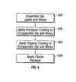
- FIG. 6is a flowchart illustrating the method applied in FIGS. 2 through 5;
- FIG. 7is a cross-sectional view showing a plastic packaged device, the die attach substrate, including the plastic package, integrated semiconductor circuit die, the wires and the leads within the plastic package, having been encapsulated by an inorganic coating;
- FIG. 8is a cross-sectional view showing the die/substrate/wire/lead/package structure with the inorganic coating encapsulating the die/substrate/wire/lead/package structure and an organic coating applied over the inorganic coating;
- FIG. 9shows a flowchart outlining the steps applied in FIGS. 7 through 9.
- FIG. 10is a perspective assembly view of one variation of a plastic case that benefits from the embodiments of FIGS. 2 through 8;
- FIG. 11is a perspective assembly view of another variation of the plastic case of FIG. 10;
- FIG. 12is a perspective view, partially in cross section, of a variation of a plastic package device showing a die/wire/lead structure with an inorganic coating encapsulating the die/wire/lead structure, with an organic coating applied thereover, such as in FIG. 4, and further showing the die/wire/lead structure packaged within a plastic package, such as in FIG. 5, forming a die/substrate/wire/lead/package structure, the die/substrate/wire/lead/package structure being shown with another inorganic coating encapsulating the die/substrate/wire/lead/package structure and another organic coating applied over the other inorganic coating, such as in FIG. 8 .
- FIG. 1Aa cross-sectional view is shown of a plastic package structure 10 (or plastic encapsulated microelectronic (PEM) device), including the plastic package 12 , a die attach substrate 14 , an integrated semiconductor circuit die 16 , wires 18 , wire bonds 20 and leads 22 .
- the leads 22form part of a lead frame prior to assembly of the plastic package structure. The lead frame holds and aligns the leads 22 until the leads are encapsulated at respective interior ends of the leads by the plastic package.
- the die 16 and die attach substrate 14are positioned near a center of the lead frame, near the interior ends 24 of the leads 22 , and wire bonds 20 are formed in a conventional manner, such as by thermocompression, thermosonic ultrasonic bonding, between bond pads 26 on the integrated semiconductor circuit die 16 , and the interior ends 24 of the leads 22 .
- wire bonds 20are formed by bonding a first end 28 of each of the wires to a respective bond pad 26 on the die 16 , and by bonding a second end 30 of each of the wires to a respective one of the interior ends 24 of the leads 22 .
- the resulting structure(such as is shown in FIG. 2) is encapsulated in the plastic package 12 , such as by injection molding.
- This encapsulation of the resulting structureincludes leaving exterior ends 32 of the leads 22 exposed and protruding from the plastic package 12 , so that the are available for connection to an electrical system, such as by soldering the exterior ends 32 of the leads 22 to a printed circuit board.
- an electrical systemsuch as by soldering the exterior ends 32 of the leads 22 to a printed circuit board.
- plastic package integrated circuit devicerepresents just one plastic package device known in the art, a dual inline pin device.
- plastic package integrated semiconductor circuit of FIG. 1Aand the examples described below, should be appreciated as just that, examples.
- the above-described plastic packaged integrated semiconductor circuitis susceptible to the infusion and moisture and other contaminants, such as oxygen, which can cause the corrosion or oxidation of the wires, the wire bonds, and the integrated semiconductor circuit die.
- contaminantsenter the plastic package through cracks, such as may form between the plastic package and the exterior ends of the leads where the exterior ends of the leads exit the plastic package; and in some cases may enter by diffusing through the plastic package itself.
- FIG. 1Ba partial cross section view is shown illustrating various failure modes addressed by the embodiments described herein. These include infiltration of moisture and ions through the plastic package, package delamination 100 , chemical contamination from agents in the plastic package 102 , ball bond fracture 104 , package cracks, and the like.
- FIGS. 2 through 6 belowrepresent one approach in accordance with the teachings herein for hermetically sealing the integrated semiconductor circuit die, wires, and wire bonds so as to prevent the infusion of contaminants, and thus contamination and ultimately failure of the plastic packaged system.
- FIG. 2(and step 600 in FIG. 6 ), shown is an assembly made up of the die, the wires, the wire bonds and the leads (which, as mentioned above are, at this point, part of a lead frame).
- This assemblysuch as may be used in the plastic package system of FIG. 1 is also one possible starting point for the present embodiments.
- the wiresare connected electrically between respective bonding pads on an upper surface of the integrated semiconductor circuit die and respective leads of the lead frame.
- the bonding of the wires to the bonding pads and to the leadsmay be achieved in a conventional manner using, for example, thermocompression, thermosonic ultrasonic bonding techniques, as are well known in the art.
- an assemblymade up of the integrated semiconductor circuit die 16 , the wires 18 , the wire bonds 20 and the leads 22 .
- a first layer 300 of a duplex coatingis a layer of an inorganic ceramic-like material applied so as to encapsulate the integrated semiconductor circuit die 16 , the wire bonds 20 , the wires 18 , and the interior ends 24 of the leads 22 .
- Encapsulation of the integrated semiconductor circuit die, the wires, the wire bonds and the leads with the first layer of the duplex coating, i.e., the inorganic ceramic like materialis preferably effected by non-line-of-sight processes such as CVD, PECVD, metalorganic chemical vapor deposition and sputtering at temperatures below approximately 300 C.
- non-line-of-sight processessuch as CVD, PECVD, metalorganic chemical vapor deposition and sputtering at temperatures below approximately 300 C.
- the preferred techniquesuse a low pressure chamber with the chemicals introduced in a vapor phase, although other approaches are contemplated, such as atmospheric pressure processes.
- ALDatomic layer deposition
- Atomic layer depositionALD and atomic layer epitaxial (ALE), and their companion technique metalorganic chemical vapor deposition (MOCVD), are well suited to producing layered structures, either epitaxial or non-epitaxial.
- Metalorganic chemical vapor depositioncan also deposit thicker monolithic layers. A large number of materials can be deposited by these techniques.
- Dielectrics which may be deposited by atomic layer epitaxial (ALE) in polycrystalline or amorphous forminclude, for example, aluminum nitride, silicon nitride, silicon carbide, alumina, titania, zirconia, hafnia, silica, magnesia, yttria, ceria, niobium oxide, tantalum oxide, lanthanum oxide, strontium titanate and barium titanate.
- ALEatomic layer epitaxial
- Thin-film technologymakes it possible to deposit a very thin (down to a few atoms in thickness) layer of material on a substrate or surface. With proper system design, both metalorganic chemical vapor deposition and atomic layer epitaxial modes can be carried out in the same deposition system.
- the thin films grown by the metalorganic chemical vapor deposition techniqueare either textured polycrystalline or epitaxial single crystal depending on the substrates used.
- Atomic layer epitaxyis a special modification of the chemical vapor deposition technique for depositing thin films and related surface structures.
- the unique feature of atomic layer epitaxialis the self-limiting film growth mechanism which gives it a number of attractive properties, like accurate and simple film thickness control, sharp interfaces, uniformity over large areas, excellent conformality, good reproducibility, multilayer processing capability, and high film qualities at relatively low temperatures.
- Thickness controlis simple and precise since the deposition is ‘pulsed’ and each pulse deposits the same thickness increment.
- High quality filmscan be deposited at low temperatures.
- the deposition rateis low (less than 5000 A/hr) but the quality of the film may be so high that thinner layers are as effective as thick layers from ‘cruder’ processes.
- thisis a gaseous-based process, large volumes of materials can be uniformly coated at one time, so the throughput in terms of the number of parts coated per hour could be competitive or better than other techniques that are more difficult to scale up.
- the metalorganic chemical vapor deposition techniqueuses liquid metalorganic precursors which vaporize in a carrier gas stream before reaching the substrate surface.
- the carrier gascan be either oxidizing (air, oxygen) or non-oxidizing such as hydrogen, nitrogen or argon.
- the formation of the desired compoundoccurs via the pyrolysis of the metalorganics and the subsequent recombination of the atomic or molecular species at or near the heated substrate.
- Liquid metalorganic precursors with relatively high vapor pressuresare preferred if they are safe, especially if no toxic byproducts are produced.
- the deposition ratescan be as high as 10 ⁇ m/h.
- the metalorganic chemical vapor deposition chambercan be optimized to deposit over large areas.
- CCVDcombustion chemical vapor deposition
- Advantagesinclude an order-of-magnitude reduction in operating and capital costs, improved materials quality and performance characteristics, and the ability to tailor-make materials for specific applications (including multi-layered structures).
- combustion chemical vapor deposition's relative ease-of-usepermits rapid development of new coating/substrate combinations.
- combustion chemical vapor deposition (CCVD) processhas demonstrated its potential to address the aforementioned requirements.
- Combustion chemical vapor deposition technologyhas significant promise to overcome many of the shortcomings of traditional vapor deposition techniques while yielding equal and/or better quality coatings at a lower cost.
- One advantage of the CCVD technologyis its ability to deposit thin films in the open atmosphere using inexpensive precursor chemicals in solution. This obviates the need for costly furnaces, vacuum equipment, reaction chambers, and post-deposition treatment (e.g. annealing). As a result, capital requirements and operating costs are reduced at least tenfold when compared to competing vacuum-based technologies (e.g. sputtering and metalorganic chemical vapor deposition).
- the ability to deposit thin films in the open atmosphereenables continuous, production-line manufacturing. Consequently, throughput potential is far greater than with conventional thin-film technologies, most of which are generally restricted to batch processing.
- precursorsare dissolved in a solvent, which typically also acts as the combustible fuel.
- This solutionis atomized to form submicron droplets by means of NANOMISER technology, owned by MicroCoating Technologies, Inc., of Georgia.
- the dropletsare then convected by an oxygen stream to a flame where they are combusted.
- a substrateis coated by simply drawing it over the flame plasma. The heat from the flame provides the energy required to evaporate the droplets and for the precursors to react and to deposit on the substrates.
- flame temperaturescan be in excess of 800° C.
- the substratemay dwell in the flame zone only briefly thus remaining cool ( ⁇ 100° C.).
- the substratecan be actively cooled.
- Substrate temperatureis therefore an independent process parameter that can be varied to actively control the film's microstructure. The process generally takes no more than two hours from set-up to post-deposition cleaning.
- the combustion chemical vapor deposition processis well-suited for high-rate deposition (up to 1 ⁇ m/min.) of dielectrics such as SiO 2 .
- diamond-like carbonshows a great deal of promise. It can be deposited to present either a hydrophobic or a hydrophilic surface to the ‘outside world’.
- GORE-TEXa fluorocarbon foam tape, that conforms by flowing tightly around irregular surfaces (such as rectangular cross section leads on integrated semiconductor circuit die devices) when compressed may be used as a masking material. This material may be too expensive, however, unless it can be sufficiently reusable. Reusable cast rubber molds (commercially available to protect connectors during soldering operations) can provide a more cost effective alternative, as can polyimide tape, tape, organic maskants, metal masks, rubber masks, and plastic masks.
- a UV lasermay provide one mechanism for stripping the coating, by ablating the coating from the leads.
- any ceramic or glassy materialis suitable as the first layer of the duplex coating.
- the materialshould be electrically insulating, e.g., greater than 10 8 ohm-meters; able to be deposited as a conformal film around all the constituent assembled parts of the device; able to be deposited as an essentially pin-hole-free coating, e.g., having a moisture permeability of less than 10 ⁇ 10 g/cm-sec-torr; able to be deposited at a temperature low enough to avoid detrimental effects to the device and constituents, e.g., at less than 300° C.
- Preferred ceramic materialsare oxide ceramics (including alumina, titania and zirconia) silicon-based ceramics (including silicon nitride, silicon oxide and silicon oxynitrides) and diamond-like carbons in amorphous or crystalline forms.
- any thickness able to reliably produce a coherent, essentially pin-hole-free filmis satisfactory (typically in excess of 500-1000 Angstroms). Thicker films improve the degree of hermeticity (unless they self-destruct from internal stresses). 5000-10,000 Angstroms is a practical upper limit for economic reasons.
- an assemblymade up of the integrated semiconductor circuit die 16 , the wires 18 , the wire bonds 20 , the leads 22 , and the first layer 300 of the duplex coating.
- a second layer 400 of the duplex coatingis a layer of an organic overcoat applied so as to encapsulate the integrated semiconductor circuit die, the wire bonds, the wires, the interior ends of the leads, and the first layer of the duplex coating.
- Encapsulation of the integrated semiconductor circuit die, the wires, the wire bonds, the leads and the first layer of the duplex coating with the second layer of the duplex coating, i.e., the organic overcoatis preferably effected by applying a layer of PARYLENE C, a form of para-xylylene.
- PARYLENE Chas many ideal properties for this part of the duplex coating.
- Other PARYLENE formulationsmay also be suitable in various embodiments.
- the thickness of the coatingshould preferably be optimized. Thicker coatings will increase the rigidity of the bond wires, be a better cushion against the abrasive and stress effects of the molding compound and provide better physical protection of the ceramic layer. However, thicker coatings are more expensive to apply and will reduce the heat dissipation of the die through the package when applied internally.
- sol-gel hybridsor sol-gel derivative materials, or fluoropolymer-silica hybrids
- sol-gel hybridswhich differ significantly from conventional sol-gels.
- These materialsmay be applied thick enough to act as a compliant layer or external scratch resistant layer as an alternative to PARYLENE, since they should have a significantly lower permeability and be harder than PARYLENE.
- Sol-gel hybrid coatingscan also be applied as a hard thin layer, one that may even qualify as a barrier layer, but also as a leveling layer, should one become necessary or desirable before application of the first layer.
- As a leveling layerit should be far superior to FOx (flowable oxide) since it can be cured in minutes at 40 to 80° C. in air as opposed to hours at 250-450° C. or higher (in a nitrogen atmosphere) for the FOx coating.
- FOxflowable oxide
- the fluoropolymer-silica hybridsare a new generation of super-adherent coatings having the combined properties of the constituent coating materials: good chemical and excellent water resistance, polymer flexibility, hydrophobicity (water repellency), low surface energy, low dielectric constant and thermal stability (above 200° C.), combined with high transparency, hardness and mechanical strength of the silica network
- the second layerextends beyond the first layer, such layers may not overlap in practice so that masking efficiency can be achieved, i.e., so that the mask does not have to be removed and repositioned between coatings.
- the inorganic ceramic-like material of the first layer of the duplex coatingserves as a primary barrier layer to moisture and ionic contamination.
- the organic overcoat of the second layer of the duplex coatingalso has some barrier properties but it also provides a physical protective layer for the thinner, more brittle inorganic ceramic-like material of the first layer of the duplex coating. Both layers are electrically insulating.
- any organic materialis suitable as the organic overcoat of the second layer of the duplex coating.
- the materialshould be electrically insulating, e.g., greater than 10 8 ohm-m resistivity; able to be deposited as a conformal film around all the constituent assembled parts of the device without damage to the first layer; able to be deposited as an essentially pin-hole-free coating, e.g., less than 0.5 g-mil/100 in 2 moisture barrier transmission rate; able to be deposited at a temperature low enough to avoid detrimental effects to the device and constituents; able to be readily built up into thicknesses to at least 0.5 mils, e.g., preferably between 1 and 3 mils; adherent to the first layer so as not to delaminate or bubble in the presence of moisture or ions; compliant and tear resistant, e.g., having an elongation ability of 10% or more; impervious to moisture, alkali metal ions and halogen ions; non-reactive and otherwise compatible (
- the second layer of the duplex layeris applied directly over the top of the first layer and, as mentioned above, is preferably PARYLENE C, other grades of PARYLENE, sol-gel hybrids, or other condensed or plasma polymerized organic films.
- PARYLENE Cis an excellent moisture and ion barrier for an organic material, is an electrical insulator, is pinhole free in sub-micron thick films yet can easily be deposited in layers over 25-75 microns thick. Thick films over 25 microns thick provide rigidity to fragile bond wires during molding and its malleability provides protection from abrasive particles in the molding resin and decouples stresses between components and the molding compound.
- the first layeris a barrier layer and has as its primary function the prevention of moisture and/or ion passage.
- the second layeris a compliant or protective layer and has as its primary function the protection of the more brittle first layer during handling and manufacture, such as injection molding.
- the duplex coatingis preferably applied to partially assembled lead frames containing attached dice and wire bonds, i.e. at the stage just prior to when the parts are transfer molded in standard commercial practices.
- a completed plastic package devicemade up of the integrated semiconductor circuit die 16 , the wires 18 , the wire bonds 20 , the leads 22 , the first layer 300 of the duplex coating, the second layer 400 of the duplex coating, and a die attach substrate 14 .
- a plastic package 12having been injection molded in a convention manner over the integrated semiconductor circuit die 16 , the wires 18 , the wire bonds 20 , the leads 22 , the first layer 300 of the duplex coating, the second layer 400 of the duplex coating, and the die attach substrate 14 .
- plastic package 12is applied in a conventional manner is it noted that conventional additives, added to protect against moisture and ions may not be needed in plastic packages in accordance with which the present embodiment or other embodiments described herein are employed.
- the duplex coating of the present embodimentprovides a hermetic barrier that protects the integrated semiconductor circuit die, the wires, and the wire bonds from contaminants, such as water and oxygen that enter the plastic package.
- the present embodimentthus provides a plastic packaged, yet hermetic integrated semiconductor circuit device, thereby achieving the economic advantages associated with plastic package devices, while achieving the high-reliability and long-life advantages of ceramic packaged devices.
- embodiments described hereinprovide much greater packaging flexibility than conventional ceramic packaging designs, while allowing operation in chemically severe environments.
- the first layeris in contact with the integrated semiconductor circuit die, such contact is not needed. As illustrated below, see FIG. 8, all that is needed is for the first layer to envelope the integrated semiconductor circuit die.
- FIG. 8illustrates a plastic package interposed between the first layer and the integrated semiconductor circuit die, it is contemplated that one or more additional layers of coating may be interposed between the first layer and the integrated semiconductor circuit die, with the plastic package also so being interposed, or being outside the first layer as in FIG. 5 .
- one or more additional layers, or the plastic packagemay be interposed between the first layer and the second layer, with (which is not preferred) or without (which is preferred) the plastic package being so interposed.
- the second layermay envelope the first layer.
- One or more tertiary layersmay also envelope the second layer, just as the plastic package envelops the second layer in FIG. 8 .
- the present embodimentis not limited to just two coating layers, or such that the inorganic first layer and the organic second layer are in contact. Similarly, the first layer need not be in contact with the integrated semiconductor circuit die.
- this same duplex coatingas described above, can also be applied, in another embodiment, over the plastic package of a conventional plastic packed system in order to provide much of the same protection as is provided by application of the duplex coating to bare assembly of the integrated semiconductor circuit die, the wire bonds, the wires, and the lead of the lead frame.
- a cross-sectional viewis shown of a plastic package structure, such as in FIG. 1, including the plastic package 12 , the die attach substrate 14 , the integrated semiconductor circuit die 16 , the wires 18 , the wire-bonds 20 and the leads 22 .
- the first layer 300 of the duplex coatingis a layer of an inorganic ceramic-like material applied, however, so as to encapsulate the plastic package 12 , and the proximal portion of the exterior ends 24 of the leads 22 .
- Application and composition of the first layer 300 of the duplex coatingis substantially as described above in reference to FIG. 3, except of course in the present embodiment, the first layer 300 is applied so as to encapsulate the plastic package 12 and its contents, as opposed to just the integrated semiconductor circuit die, wire bonds, wires, and interior ends of the leads.
- FIG. 9, Block 900the assembly comprising the integrated semiconductor circuit die, wire bonds, wires, and leads is formed in a conventional manner as described above.
- FIG. 9, Block 902the assembly, with the exception of the exterior ends of the leads, is encapsulated in the plastic package, as also described above.
- the first layer of the duplex coatingis applied, substantially as described above, but so as to encapsulate the plastic package and its contents, as opposed to just the integrated semiconductor circuit die, wire bonds, wires, and interior ends of the leads.
- the thickness of the second layermay also be greater in the present embodiment in that more handling of the second coating would be expected than in the prior embodiment.
- a cross-sectional viewis shown of a plastic package structure, such as in FIG. 1, including the plastic package 12 , the die attach substrate 14 , the integrated semiconductor circuit die 16 , the wires 18 , the wire-bonds 20 and the leads 22 .
- the first layer 300 of the duplex coatingas in FIG. 7 .
- the second layer 400 of the duplex coatingis a layer of an organic overcoat applied, however, so as to encapsulate the plastic package 12 , and the proximal portion of the exterior ends 32 of the leads 22 , and the first layer 300 of the duplex coating.
- the second layer of the duplex coatingis substantially as described above in reference to FIG. 4, except of course in the present embodiment, the second layer is applied so as to encapsulate the plastic package and its contents as well as the first layer of the duplex coating, as opposed to just the integrated semiconductor circuit die, wire bonds, wires, interior ends of the leads, and the first layer of the duplex coating.
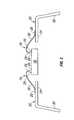
- FIG. 10shown is an assembly view of a plastic case structure in which the principles described herein may be incorporated. Shown are a plastic cap, a first epoxy seal, a lead frame, an integrated semiconductor circuit die, wires and wire bonds, a second epoxy seal, and a plastic base.
- the illustrated assemblyis conventional in structure and manufacturing except that prior to assembly, the duplex coating described above is applied to the integrated semiconductor circuit die 1006 , the wire bonds 1010 , the wires 1008 , and interior ends of leads of the lead frame.
- Masking of or removal of the duplex coating from exterior ends of the leads of the lead frameis effected as described above in order to maintain the exterior ends of the leads for electrical connection.
- FIG. 11shown is an assembly view of another plastic case structure in which the principles described herein may be incorporated. Shown in a plastic cap 2000 , a first epoxy seal 2002 , a plastic side wall 2004 , a second epoxy seal 2006 , a lead frame 2008 , an integrated semiconductor circuit die 2010 , wires 2012 and wire bonds 2014 , a third epoxy seal 2016 , and a plastic base 2018 .
- the illustrated assemblyis conventional in structure and manufacturing except, as with the embodiment of FIG. 10, prior to assembly, the duplex coating described above is applied to the integrated semiconductor circuit die 2010 , the wire bonds 2014 , the wires 2012 , and interior ends of leads of the lead frame 2008 .
- masking of or removal of the duplex coating from exterior ends of the leads of the lead frameis effected as described above in order to maintain the exterior ends of the leads for electrical connection.
- FIG. 12a perspective view is shown, partially in cross section, of a device having both the coating approach of FIGS. 2 through 6 and the coating approach of FIGS. 7 through 9 applied thereto.
- the approach of the illustrated embodimentis identical to the individual approaches described in reference to these groups of figures, except that both approaches are applied to the same device, further explanation of these approaches is not made herein.
- the illustrated embodimentmay provide even greater hermeticity than either of the approaches described above in their numerous variations.
Landscapes
- Engineering & Computer Science (AREA)
- Computer Hardware Design (AREA)
- Microelectronics & Electronic Packaging (AREA)
- Power Engineering (AREA)
- Physics & Mathematics (AREA)
- Condensed Matter Physics & Semiconductors (AREA)
- General Physics & Mathematics (AREA)
- Structures Or Materials For Encapsulating Or Coating Semiconductor Devices Or Solid State Devices (AREA)
- Encapsulation Of And Coatings For Semiconductor Or Solid State Devices (AREA)
- Control And Other Processes For Unpacking Of Materials (AREA)
Abstract
Description
Claims (16)
Priority Applications (12)
| Application Number | Priority Date | Filing Date | Title |
|---|---|---|---|
| US09/520,928US6368899B1 (en) | 2000-03-08 | 2000-03-08 | Electronic device packaging |
| JP2001566180AJP2003526920A (en) | 2000-03-08 | 2001-03-07 | Electronic device packaging |
| MXPA02008736AMXPA02008736A (en) | 2000-03-08 | 2001-03-07 | PACKAGING FOR ELECTRONIC DEVICE. |
| BR0109077-1ABR0109077A (en) | 2000-03-08 | 2001-03-07 | Hermetically coated device and method of manufacture |
| EP01913337AEP1269531A1 (en) | 2000-03-08 | 2001-03-07 | Electronic device packaging |
| KR1020027011713AKR20030003696A (en) | 2000-03-08 | 2001-03-07 | Electronic device packaging |
| IL15149801AIL151498A0 (en) | 2000-03-08 | 2001-03-07 | Electronic device packaging |
| PCT/US2001/007281WO2001067504A1 (en) | 2000-03-08 | 2001-03-07 | Electronic device packaging |
| CN01806244ACN1416593A (en) | 2000-03-08 | 2001-03-07 | Electronic device packaging |
| CA002401702ACA2401702A1 (en) | 2000-03-08 | 2001-03-07 | Electronic device packaging |
| AU2001242012AAU2001242012A1 (en) | 2000-03-08 | 2001-03-07 | Electronic device packaging |
| US10/075,706US6963125B2 (en) | 2000-03-08 | 2002-02-13 | Electronic device packaging |
Applications Claiming Priority (1)
| Application Number | Priority Date | Filing Date | Title |
|---|---|---|---|
| US09/520,928US6368899B1 (en) | 2000-03-08 | 2000-03-08 | Electronic device packaging |
Related Child Applications (1)
| Application Number | Title | Priority Date | Filing Date |
|---|---|---|---|
| US10/075,706ContinuationUS6963125B2 (en) | 2000-03-08 | 2002-02-13 | Electronic device packaging |
Publications (1)
| Publication Number | Publication Date |
|---|---|
| US6368899B1true US6368899B1 (en) | 2002-04-09 |
Family
ID=24074614
Family Applications (2)
| Application Number | Title | Priority Date | Filing Date |
|---|---|---|---|
| US09/520,928Expired - LifetimeUS6368899B1 (en) | 2000-03-08 | 2000-03-08 | Electronic device packaging |
| US10/075,706Expired - LifetimeUS6963125B2 (en) | 2000-03-08 | 2002-02-13 | Electronic device packaging |
Family Applications After (1)
| Application Number | Title | Priority Date | Filing Date |
|---|---|---|---|
| US10/075,706Expired - LifetimeUS6963125B2 (en) | 2000-03-08 | 2002-02-13 | Electronic device packaging |
Country Status (11)
| Country | Link |
|---|---|
| US (2) | US6368899B1 (en) |
| EP (1) | EP1269531A1 (en) |
| JP (1) | JP2003526920A (en) |
| KR (1) | KR20030003696A (en) |
| CN (1) | CN1416593A (en) |
| AU (1) | AU2001242012A1 (en) |
| BR (1) | BR0109077A (en) |
| CA (1) | CA2401702A1 (en) |
| IL (1) | IL151498A0 (en) |
| MX (1) | MXPA02008736A (en) |
| WO (1) | WO2001067504A1 (en) |
Cited By (45)
| Publication number | Priority date | Publication date | Assignee | Title |
|---|---|---|---|---|
| US20020050371A1 (en)* | 1993-06-18 | 2002-05-02 | Czjakowski David R. | Radiation shielding of three dimensional multi-chip modules |
| US20020089069A1 (en)* | 2000-11-20 | 2002-07-11 | Lamson Michael A. | Low capacitance coupling wire bonded semiconductor device |
| US20020113322A1 (en)* | 2000-06-12 | 2002-08-22 | Shinichi Terashima | Semiconductor device and method to produce the same |
| US20030176080A1 (en)* | 2002-03-13 | 2003-09-18 | Haiying Fu | Hermetic silicon carbide |
| US6649446B1 (en)* | 2001-11-29 | 2003-11-18 | Clarisay, Inc. | Hermetic package for multiple contact-sensitive electronic devices and methods of manufacturing thereof |
| US6726996B2 (en)* | 2001-05-16 | 2004-04-27 | International Business Machines Corporation | Laminated diffusion barrier |
| US20040175905A1 (en)* | 2003-03-04 | 2004-09-09 | Won Seok-Jun | Method of forming thin film using atomic layer deposition |
| US20040178498A1 (en)* | 2003-03-10 | 2004-09-16 | Low Qwai H. | Wire bonding to full array bonding pads on active circuitry |
| US20040259291A1 (en)* | 2003-06-23 | 2004-12-23 | Sandisk Corporation | Method for efficiently producing removable peripheral cards |
| US20040262749A1 (en)* | 2003-06-30 | 2004-12-30 | Matayabas J. Christopher | Wire-bonded package with electrically insulating wire encapsulant and thermally conductive overmold |
| US6847122B1 (en) | 2003-10-16 | 2005-01-25 | Kulicke & Soffa Investments, Inc. | System and method for preventing and alleviating short circuiting in a semiconductor device |
| US6852567B1 (en)* | 1999-05-31 | 2005-02-08 | Infineon Technologies A.G. | Method of assembling a semiconductor device package |
| US20050085019A1 (en)* | 2003-10-16 | 2005-04-21 | Rakesh Batish | System and method for reducing or eliminating semiconductor device wire sweep |
| US20050116357A1 (en)* | 2002-10-31 | 2005-06-02 | International Business Machines Corporation | Method and structure to enhance temperature/humidity/bias performance of semiconductor devices by surface modification |
| US20050121798A1 (en)* | 2003-10-16 | 2005-06-09 | Kulicke & Soffa Investments, Inc. | Method for reducing or eliminating semiconductor device wire sweep in a multi-tier bonding device and a device produced by the method |
| US20050145994A1 (en)* | 2004-01-06 | 2005-07-07 | International Business Machines Corporation | Compliant passivated edge seal for low-k interconnect structures |
| US20050255628A1 (en)* | 2003-09-18 | 2005-11-17 | Micron Technology, Inc. | Microelectronic devices and methods for packaging microelectronic devices |
| US20060035402A1 (en)* | 2004-08-10 | 2006-02-16 | Street Bret K | Microelectronic imaging units and methods of manufacturing microelectronic imaging units |
| DE102004047510A1 (en)* | 2004-09-28 | 2006-04-13 | Infineon Technologies Ag | Semiconductor device having semiconductor device components embedded in plastic package |
| US20060102597A1 (en)* | 2004-11-16 | 2006-05-18 | Exponent, Inc. | Electron beam welding method and apparatus using controlled volumetric heating |
| DE102005025465A1 (en)* | 2005-05-31 | 2006-12-14 | Infineon Technologies Ag | Semiconductor unit comprises a circuit carrier with interior contact areas, a semiconductor chip with an active surface and flipside and bonding wire connections between chip contact areas and interior contact areas of the circuit carrier |
| DE102005061248A1 (en)* | 2005-12-20 | 2007-06-28 | Infineon Technologies Ag | Semiconductor device having semiconductor device components embedded in plastic package |
| KR100762878B1 (en) | 2006-01-23 | 2007-10-08 | 주식회사 하이닉스반도체 | Planner Stack Package |
| US20080096317A1 (en)* | 2006-10-20 | 2008-04-24 | Warren Middlekauff | Method for producing portable memory devices |
| US7382043B2 (en) | 2002-09-25 | 2008-06-03 | Maxwell Technologies, Inc. | Method and apparatus for shielding an integrated circuit from radiation |
| US20080128876A1 (en)* | 2006-11-30 | 2008-06-05 | Chenglin Liu | Chip on leads |
| US20080157307A1 (en)* | 2006-12-28 | 2008-07-03 | Semiconductor Manufacturing International (Shanghai) Corporation | Lead frame |
| US20080185582A1 (en)* | 2006-10-20 | 2008-08-07 | Warren Middlekauff | Portable memory devices |
| US20080251895A1 (en)* | 2003-07-16 | 2008-10-16 | Janet Patterson | Apparatus for shielding integrated circuit devices |
| DE102007035608A1 (en)* | 2007-07-30 | 2009-02-05 | Infineon Technologies Ag | Semiconductor module, has connecting element connecting electrode of semiconductor chip with contact connection surface of substrate, and semiconductor chip, connecting element and substrate embedded in cover of flexible group layer |
| US20090146268A1 (en)* | 2007-12-07 | 2009-06-11 | Rui Huang | Integrated circuit package system for electromagnetic isolation |
| US20100044841A1 (en)* | 2008-08-20 | 2010-02-25 | Infineon Technologies Ag | Semiconductor device |
| US20100119843A1 (en)* | 2008-11-10 | 2010-05-13 | Applied Materials, Inc. | Plasma resistant coatings for plasma chamber components |
| US20120313296A1 (en)* | 2011-06-10 | 2012-12-13 | Aliphcom | Component protective overmolding |
| US20120313272A1 (en)* | 2011-06-10 | 2012-12-13 | Aliphcom, Inc. | Component protective overmolding |
| US9069380B2 (en) | 2011-06-10 | 2015-06-30 | Aliphcom | Media device, application, and content management using sensory input |
| WO2014028408A3 (en)* | 2012-08-13 | 2015-07-16 | Aliphcom | Component protective overmolding using protective external coatings |
| EP1843816B1 (en)* | 2005-02-01 | 2017-07-12 | Second Sight Medical Products, Inc. | Micro-miniature implantable coated device |
| US20170338169A1 (en)* | 2016-05-20 | 2017-11-23 | Infineon Technologies Ag | Chip package, method of forming a chip package and method of forming an electrical contact |
| US20180174936A1 (en)* | 2016-12-15 | 2018-06-21 | Infineon Technologies Ag | Power Semiconductor Modules with Protective Coating |
| US20180350780A1 (en)* | 2016-04-04 | 2018-12-06 | Infineon Technologies Ag | An Electronic Device Package |
| US10811371B2 (en) | 2016-01-14 | 2020-10-20 | Mitsubishi Electric Corporation | Semiconductor device and manufacturing method thereof |
| US11264296B2 (en) | 2018-08-07 | 2022-03-01 | Corning Incorporated | Hermetically sealed package |
| US11552006B2 (en)* | 2020-07-22 | 2023-01-10 | Texas Instruments Incorporated | Coated semiconductor devices |
| US20240321663A1 (en)* | 2023-03-22 | 2024-09-26 | Wolfspeed, Inc. | High-performance stress buffer die-coat and devices and processes implementing the same |
Families Citing this family (34)
| Publication number | Priority date | Publication date | Assignee | Title |
|---|---|---|---|---|
| US7723162B2 (en)* | 2002-03-22 | 2010-05-25 | White Electronic Designs Corporation | Method for producing shock and tamper resistant microelectronic devices |
| KR20060006840A (en) | 2003-05-16 | 2006-01-19 | 이 아이 듀폰 디 네모아 앤드 캄파니 | Barrier film for plastic substrate produced by atomic layer deposition |
| DE102004015403A1 (en)* | 2004-03-26 | 2005-11-03 | Infineon Technologies Ag | Use of nanoscale particles for the production of scratch-resistant protective coatings on semiconductor chips |
| US7705432B2 (en)* | 2004-04-13 | 2010-04-27 | Vertical Circuits, Inc. | Three dimensional six surface conformal die coating |
| ES2559410T3 (en)* | 2004-04-23 | 2016-02-12 | Philip Morris Products S.A. | Aerosol generators and methods for producing aerosols |
| US8501277B2 (en)* | 2004-06-04 | 2013-08-06 | Applied Microstructures, Inc. | Durable, heat-resistant multi-layer coatings and coated articles |
| JP2006118669A (en)* | 2004-10-25 | 2006-05-11 | Sanoh Industrial Co Ltd | Resin tube |
| US7409878B2 (en)* | 2005-04-08 | 2008-08-12 | Honeywell International Inc. | Torqueshaft magnetic field measurement systems for gas turbine engines |
| CN100399037C (en)* | 2005-04-30 | 2008-07-02 | 中国科学院空间科学与应用研究中心 | A Screening Method for Spatial Applications of Commercial Plastic Packaged Devices |
| DE102005025083B4 (en)* | 2005-05-30 | 2007-05-24 | Infineon Technologies Ag | Thermoplastic thermoset composite and method for bonding a thermoplastic material to a thermoset material |
| DE102005028704B4 (en)* | 2005-06-20 | 2016-09-08 | Infineon Technologies Ag | A method of manufacturing a semiconductor device having semiconductor device components embedded in plastic package |
| US20070135552A1 (en)* | 2005-12-09 | 2007-06-14 | General Atomics | Gas barrier |
| DE112006003861B4 (en)* | 2006-05-10 | 2015-09-17 | Infineon Technologies Ag | Semiconductor module and method for producing a semiconductor module |
| US8110906B2 (en)* | 2007-01-23 | 2012-02-07 | Infineon Technologies Ag | Semiconductor device including isolation layer |
| US7923823B2 (en)* | 2007-01-23 | 2011-04-12 | Infineon Technologies Ag | Semiconductor device with parylene coating |
| US20080248263A1 (en)* | 2007-04-02 | 2008-10-09 | Applied Microstructures, Inc. | Method of creating super-hydrophobic and-or super-hydrophilic surfaces on substrates, and articles created thereby |
| US8236379B2 (en) | 2007-04-02 | 2012-08-07 | Applied Microstructures, Inc. | Articles with super-hydrophobic and-or super-hydrophilic surfaces and method of formation |
| US7939932B2 (en)* | 2007-06-20 | 2011-05-10 | Analog Devices, Inc. | Packaged chip devices with atomic layer deposition protective films |
| US8097934B1 (en) | 2007-09-27 | 2012-01-17 | National Semiconductor Corporation | Delamination resistant device package having low moisture sensitivity |
| WO2009081723A1 (en)* | 2007-12-20 | 2009-07-02 | Fuji Electric Device Technology Co., Ltd. | Semiconductor device and method for manufacturing the same |
| US20100164083A1 (en)* | 2008-12-29 | 2010-07-01 | Numonyx B.V. | Protective thin film coating in chip packaging |
| JP5150597B2 (en)* | 2009-10-08 | 2013-02-20 | 新電元工業株式会社 | Semiconductor package and manufacturing method thereof |
| DE102009058796A1 (en) | 2009-12-18 | 2011-06-22 | OSRAM Opto Semiconductors GmbH, 93055 | Optoelectronic component and method for producing an optoelectronic component |
| JP5427680B2 (en)* | 2010-04-14 | 2014-02-26 | 株式会社金陽社 | Manufacturing method of organic thin film solar cell |
| US20120166665A1 (en)* | 2010-12-22 | 2012-06-28 | Research In Motion Limited | Method and system for selectively performing proxy services |
| JP5956783B2 (en)* | 2012-03-02 | 2016-07-27 | ルネサスエレクトロニクス株式会社 | Manufacturing method of semiconductor device |
| US20150040388A1 (en)* | 2012-03-20 | 2015-02-12 | Applied Nanotech Holdings, Inc. | Application of Dielectric Layer and Circuit Traces on Heat Sink |
| DE102012108770A1 (en)* | 2012-09-18 | 2014-03-20 | Rudolf Heicks | Electronic assembly with a spatially injection-molded electronic circuit carrier |
| US20140141191A1 (en)* | 2012-11-20 | 2014-05-22 | Veeco Ald Inc. | Hydrophobic and Oleophobic Encapsulation Material with Alternating Layers |
| US9233842B2 (en)* | 2013-03-15 | 2016-01-12 | Robert Bosch Gmbh | Passivation layer for harsh environments and methods of fabrication thereof |
| JP6064928B2 (en)* | 2014-02-13 | 2017-01-25 | トヨタ自動車株式会社 | Semiconductor device |
| US10847384B2 (en)* | 2017-05-31 | 2020-11-24 | Palo Alto Research Center Incorporated | Method and fixture for chip attachment to physical objects |
| DE102024200461A1 (en) | 2024-01-18 | 2025-07-24 | Infineon Technologies Ag | SEMICONDUCTOR HOUSING AND METHOD FOR MANUFACTURING A SEMICONDUCTOR HOUSING |
| WO2025177211A1 (en)* | 2024-02-21 | 2025-08-28 | Baker Hughes Inteq Gmbh | Cost-efficient core-shell parylene coating improving wire bond stiffness and damping |
Citations (85)
| Publication number | Priority date | Publication date | Assignee | Title |
|---|---|---|---|---|
| US3646409A (en)* | 1968-07-30 | 1972-02-29 | Philips Corp | Heat-sinking package for semiconductor integrated circuit |
| US3706840A (en) | 1971-05-10 | 1972-12-19 | Intersil Inc | Semiconductor device packaging |
| US3771025A (en) | 1969-10-02 | 1973-11-06 | Gen Electric | Semiconductor device including low impedance connections |
| US3828425A (en) | 1970-10-16 | 1974-08-13 | Texas Instruments Inc | Method for making semiconductor packaged devices and assemblies |
| US3914858A (en) | 1974-08-23 | 1975-10-28 | Nitto Electric Ind Co | Method of making sealed cavity molded semiconductor devices |
| US4089575A (en) | 1976-09-27 | 1978-05-16 | Amp Incorporated | Connector for connecting a circuit element to the surface of a substrate |
| US4091407A (en) | 1976-11-01 | 1978-05-23 | Rca Corporation | Combination glass/low temperature deposited Siw Nx Hy O.sub.z |
| US4100675A (en) | 1976-11-01 | 1978-07-18 | Mansol Ceramics Company | Novel method and apparatus for hermetic encapsulation for integrated circuits and the like |
| JPS544781A (en) | 1977-06-03 | 1979-01-13 | Buichi Kataoka | Fishing rod arranging apparatus in setting and throwing machine of fishing rod with reel |
| US4173683A (en) | 1977-06-13 | 1979-11-06 | Rca Corporation | Chemically treating the overcoat of a semiconductor device |
| US4198444A (en)* | 1975-08-04 | 1980-04-15 | General Electric Company | Method for providing substantially hermetic sealing means for electronic components |
| US4250347A (en) | 1977-05-05 | 1981-02-10 | Fierkens Richardus H | Method of encapsulating microelectronic elements |
| JPS56103452A (en) | 1980-01-22 | 1981-08-18 | Fujitsu Ltd | Semiconductor device |
| JPS5795650A (en) | 1980-12-05 | 1982-06-14 | Nec Corp | Semiconductor device |
| US4468411A (en) | 1982-04-05 | 1984-08-28 | Motorola, Inc. | Method for providing alpha particle protection for an integrated circuit die |
| US4506108A (en) | 1983-04-01 | 1985-03-19 | Sperry Corporation | Copper body power hybrid package and method of manufacture |
| JPS60106150A (en) | 1983-11-15 | 1985-06-11 | Nippon Telegr & Teleph Corp <Ntt> | Radiation proof package |
| US4523372A (en) | 1984-05-07 | 1985-06-18 | Motorola, Inc. | Process for fabricating semiconductor device |
| JPS60124834A (en) | 1983-12-09 | 1985-07-03 | Nec Corp | Inspecting process of semiconductor device |
| JPS60180150A (en) | 1984-02-27 | 1985-09-13 | Nippon Telegr & Teleph Corp <Ntt> | Semiconductor device |
| EP0160327A1 (en) | 1984-03-05 | 1985-11-06 | Mitsubishi Cable Industries, Ltd. | Laminar radiation-shielding article |
| JPS614249A (en) | 1984-06-19 | 1986-01-10 | Sumitomo Electric Ind Ltd | Package for semiconductor device |
| JPS614250A (en) | 1984-06-19 | 1986-01-10 | Sumitomo Electric Ind Ltd | Package for semiconductor device |
| US4633573A (en) | 1982-10-12 | 1987-01-06 | Aegis, Inc. | Microcircuit package and sealing method |
| FR2584863A1 (en) | 1985-07-12 | 1987-01-16 | Inf Milit Spatiale Aeronaut | CURRENT ELECTRONIC COMPONENT WITH REGARD TO RADIATION |
| US4652465A (en) | 1984-05-14 | 1987-03-24 | Nissan Chemical Industries Ltd. | Process for the production of a silver coated copper powder and conductive coating composition |
| US4661837A (en) | 1982-05-28 | 1987-04-28 | Fujitsu Limited | Resin-sealed radiation shield for a semiconductor device |
| US4663240A (en) | 1984-11-06 | 1987-05-05 | Enthone, Incorporated | RFI shielded plastic articles and process for making same |
| JPS62125651A (en) | 1985-11-26 | 1987-06-06 | Nippon Telegr & Teleph Corp <Ntt> | Radiation resistant package |
| US4687622A (en) | 1985-10-29 | 1987-08-18 | Irt Corporation | Nuclear event detector |
| US4769344A (en) | 1984-06-04 | 1988-09-06 | Mitsubishi Denki Kabushiki Kaisha | Method of resin encapsulating a semiconductor device |
| US4833334A (en) | 1986-04-16 | 1989-05-23 | Aerospatiale, Societe Nationale Industrielle | Protective box for electronic circuits hardened with respect to X-rays |
| US4835120A (en) | 1987-01-12 | 1989-05-30 | Debendra Mallik | Method of making a multilayer molded plastic IC package |
| US4837448A (en) | 1986-04-16 | 1989-06-06 | Aerospatiale Societe Nationale Industrielle | Protective sheath for electrical or optical conductors hardened with respect to X-rays |
| US4839716A (en) | 1987-06-01 | 1989-06-13 | Olin Corporation | Semiconductor packaging |
| US4888449A (en) | 1988-01-04 | 1989-12-19 | Olin Corporation | Semiconductor package |
| US4891687A (en) | 1987-01-12 | 1990-01-02 | Intel Corporation | Multi-layer molded plastic IC package |
| US4935174A (en) | 1986-01-13 | 1990-06-19 | Canon Kabushiki Kaisha | Resin molded article bearing electric circuit patterns and process for producing the same |
| US4953002A (en) | 1988-03-31 | 1990-08-28 | Honeywell Inc. | Semiconductor device housing with magnetic field protection |
| JPH02237053A (en) | 1989-03-09 | 1990-09-19 | Fujitsu Ltd | Semiconductor chip mounting method |
| US4967315A (en) | 1990-01-02 | 1990-10-30 | General Electric Company | Metallized ceramic circuit package |
| JPH02278740A (en) | 1989-04-19 | 1990-11-15 | Matsushita Electric Works Ltd | Packaging of semiconductor device |
| US4975762A (en) | 1981-06-11 | 1990-12-04 | General Electric Ceramics, Inc. | Alpha-particle-emitting ceramic composite cover |
| US4979019A (en) | 1988-05-11 | 1990-12-18 | Refractory Composites, Inc. | Printed circuit board with inorganic insulating matrix |
| US5047260A (en) | 1987-02-06 | 1991-09-10 | Key-Tech, Inc. | Method for producing a shielded plastic enclosure to house electronic equipment |
| US5096851A (en) | 1988-05-19 | 1992-03-17 | Semiconductor Energy Laboratory Co., Ltd. | Method of packaging an electronic device using a common holder to carry the device in both a cvd and molding step |
| JPH0494560A (en) | 1990-08-10 | 1992-03-26 | Seiko Epson Corp | semiconductor equipment |
| US5138430A (en) | 1991-06-06 | 1992-08-11 | International Business Machines Corporation | High performance versatile thermally enhanced IC chip mounting |
| US5139969A (en) | 1990-05-30 | 1992-08-18 | Mitsubishi Denki Kabushiki Kaisha | Method of making resin molded semiconductor device |
| US5149662A (en) | 1991-03-27 | 1992-09-22 | Integrated System Assemblies Corporation | Methods for testing and burn-in of integrated circuit chips |
| US5151770A (en) | 1989-11-24 | 1992-09-29 | Mitsubishi Denki Kabushiki Kaisha | Shielded semiconductor device |
| JPH04273200A (en) | 1991-02-27 | 1992-09-29 | Toshiba Corp | Shield device |
| US5166772A (en) | 1991-02-22 | 1992-11-24 | Motorola, Inc. | Transfer molded semiconductor device package with integral shield |
| US5180513A (en) | 1987-02-06 | 1993-01-19 | Key-Tech, Inc. | Shielded plastic enclosure to house electronic equipment |
| US5202536A (en) | 1992-02-03 | 1993-04-13 | Schlegel Corporation | EMI shielding seal with partial conductive sheath |
| US5206794A (en) | 1991-12-20 | 1993-04-27 | Vlsi Technology, Inc. | Integrated circuit package with device and wire coat assembly |
| US5239126A (en) | 1990-01-17 | 1993-08-24 | Sony Corporation | High-frequency circuit package |
| US5250845A (en) | 1990-11-30 | 1993-10-05 | Hughes Aircraft Company | Totally enclosed hermetic electronic module |
| US5268331A (en) | 1992-01-07 | 1993-12-07 | Texas Instruments Incorporated | Stabilizer/spacer for semiconductor device lead frames |
| US5294826A (en) | 1993-04-16 | 1994-03-15 | Northern Telecom Limited | Integrated circuit package and assembly thereof for thermal and EMI management |
| US5304750A (en) | 1988-05-27 | 1994-04-19 | G + H Montage Gmbh | Absorber for electromagnetic and acoustic waves |
| US5317107A (en) | 1992-09-24 | 1994-05-31 | Motorola, Inc. | Shielded stripline configuration semiconductor device and method for making the same |
| US5384477A (en) | 1993-03-09 | 1995-01-24 | National Semiconductor Corporation | CMOS latchup suppression by localized minority carrier lifetime reduction |
| US5406117A (en) | 1993-12-09 | 1995-04-11 | Dlugokecki; Joseph J. | Radiation shielding for integrated circuit devices using reconstructed plastic packages |
| US5424251A (en) | 1991-03-20 | 1995-06-13 | Fujitsu Limited | Method of producing semiconductor device having radiation part made of resin containing insulator powders |
| US5527742A (en) | 1993-07-26 | 1996-06-18 | National Semiconductor Corporation | Process for coated bonding wires in high lead count packages |
| US5552338A (en) | 1994-09-26 | 1996-09-03 | Intel Corporation | Method of using latchup current to blow a fuse in an integrated circuit |
| US5561265A (en) | 1993-03-24 | 1996-10-01 | Northern Telecom Limited | Integrated circuit packaging |
| US5577319A (en) | 1995-03-31 | 1996-11-26 | Motorola, Inc. | Method of encapsulating a crystal oscillator |
| US5589129A (en) | 1993-02-19 | 1996-12-31 | Kabushiki Kaisha Toshiba | Method of manufacturing a molding using a filler or an additive concentrated on an arbitrary portion or distributed at a gradient concentration |
| US5610443A (en) | 1994-09-08 | 1997-03-11 | General Instrument Of Taiwan, Ltd. | Method for encapsulating a semiconductor utilizing an epoxy resin and an onium salt compound |
| US5629559A (en)* | 1993-04-06 | 1997-05-13 | Tokuyama Corporation | Package for semiconductor device |
| US5672918A (en) | 1994-08-18 | 1997-09-30 | The United States Of America As Represented By The United States Department Of Energy | System level latchup mitigation for single event and transient radiation effects on electronics |
| US5714102A (en) | 1992-01-02 | 1998-02-03 | International Business Machines Corporation | Method for manufacturing electro-magnetic shield having multiple polymeric layers of differing fill compositions |
| US5770304A (en) | 1994-07-11 | 1998-06-23 | Nippon Paint Co., Ltd. | Wide bandwidth electromagnetic wave absorbing material |
| US5780163A (en) | 1996-06-05 | 1998-07-14 | Dow Corning Corporation | Multilayer coating for microelectronic devices |
| US5824568A (en) | 1992-12-10 | 1998-10-20 | International Business Machines Corporation | Process of making an integrated circuit chip composite |
| US5825042A (en) | 1993-06-18 | 1998-10-20 | Space Electronics, Inc. | Radiation shielding of plastic integrated circuits |
| US5834891A (en) | 1996-06-18 | 1998-11-10 | Ppg Industries, Inc. | Spacers, spacer units, image display panels and methods for making and using the same |
| US5847467A (en)* | 1990-08-31 | 1998-12-08 | Texas Instruments Incorporated | Device packaging using heat spreaders and assisted deposition of wire bonds |
| US5851852A (en) | 1996-02-13 | 1998-12-22 | Northrop Grumman Corporation | Die attached process for SiC |
| US5864088A (en) | 1994-01-20 | 1999-01-26 | Tokin Corporation | Electronic device having the electromagnetic interference suppressing body |
| US5880403A (en) | 1994-04-01 | 1999-03-09 | Space Electronics, Inc. | Radiation shielding of three dimensional multi-chip modules |
| US5888850A (en) | 1997-09-29 | 1999-03-30 | International Business Machines Corporation | Method for providing a protective coating and electronic package utilizing same |
| US5946556A (en)* | 1998-01-09 | 1999-08-31 | Nec Corporation | Fabrication method of plastic-packaged semiconductor device |
Family Cites Families (6)
| Publication number | Priority date | Publication date | Assignee | Title |
|---|---|---|---|---|
| JPS5795850A (en) | 1980-12-04 | 1982-06-14 | Ukenori Fukushi | Method of drawing picture on glass surface and said glass picture |
| US4804625A (en) | 1984-09-27 | 1989-02-14 | Amoco Corporation | Assay procedures |
| US4625465A (en)* | 1985-12-19 | 1986-12-02 | Kirt Daryl L | Hone stop assembly |
| JPS644781A (en) | 1987-06-29 | 1989-01-09 | Olympus Optical Co | Suction type liquid developing head |
| JP2734443B2 (en)* | 1996-03-19 | 1998-03-30 | 日本電気株式会社 | Resin-sealed semiconductor device |
| US6365521B1 (en)* | 1997-12-31 | 2002-04-02 | Intel Corporation | Passivation for tight metal geometry |
- 2000
- 2000-03-08USUS09/520,928patent/US6368899B1/ennot_activeExpired - Lifetime
- 2001
- 2001-03-07WOPCT/US2001/007281patent/WO2001067504A1/ennot_activeApplication Discontinuation
- 2001-03-07ILIL15149801Apatent/IL151498A0/enunknown
- 2001-03-07BRBR0109077-1Apatent/BR0109077A/ennot_activeApplication Discontinuation
- 2001-03-07CNCN01806244Apatent/CN1416593A/enactivePending
- 2001-03-07KRKR1020027011713Apatent/KR20030003696A/ennot_activeWithdrawn
- 2001-03-07CACA002401702Apatent/CA2401702A1/ennot_activeAbandoned
- 2001-03-07AUAU2001242012Apatent/AU2001242012A1/ennot_activeAbandoned
- 2001-03-07EPEP01913337Apatent/EP1269531A1/ennot_activeWithdrawn
- 2001-03-07JPJP2001566180Apatent/JP2003526920A/enactivePending
- 2001-03-07MXMXPA02008736Apatent/MXPA02008736A/ennot_activeApplication Discontinuation
- 2002
- 2002-02-13USUS10/075,706patent/US6963125B2/ennot_activeExpired - Lifetime
Patent Citations (87)
| Publication number | Priority date | Publication date | Assignee | Title |
|---|---|---|---|---|
| US3646409A (en)* | 1968-07-30 | 1972-02-29 | Philips Corp | Heat-sinking package for semiconductor integrated circuit |
| US3771025A (en) | 1969-10-02 | 1973-11-06 | Gen Electric | Semiconductor device including low impedance connections |
| US3828425A (en) | 1970-10-16 | 1974-08-13 | Texas Instruments Inc | Method for making semiconductor packaged devices and assemblies |
| US3706840A (en) | 1971-05-10 | 1972-12-19 | Intersil Inc | Semiconductor device packaging |
| US3914858A (en) | 1974-08-23 | 1975-10-28 | Nitto Electric Ind Co | Method of making sealed cavity molded semiconductor devices |
| US4198444A (en)* | 1975-08-04 | 1980-04-15 | General Electric Company | Method for providing substantially hermetic sealing means for electronic components |
| US4089575A (en) | 1976-09-27 | 1978-05-16 | Amp Incorporated | Connector for connecting a circuit element to the surface of a substrate |
| US4100675A (en) | 1976-11-01 | 1978-07-18 | Mansol Ceramics Company | Novel method and apparatus for hermetic encapsulation for integrated circuits and the like |
| US4091407A (en) | 1976-11-01 | 1978-05-23 | Rca Corporation | Combination glass/low temperature deposited Siw Nx Hy O.sub.z |
| US4250347A (en) | 1977-05-05 | 1981-02-10 | Fierkens Richardus H | Method of encapsulating microelectronic elements |
| JPS544781A (en) | 1977-06-03 | 1979-01-13 | Buichi Kataoka | Fishing rod arranging apparatus in setting and throwing machine of fishing rod with reel |
| US4173683A (en) | 1977-06-13 | 1979-11-06 | Rca Corporation | Chemically treating the overcoat of a semiconductor device |
| JPS56103452A (en) | 1980-01-22 | 1981-08-18 | Fujitsu Ltd | Semiconductor device |
| JPS5795650A (en) | 1980-12-05 | 1982-06-14 | Nec Corp | Semiconductor device |
| US4975762A (en) | 1981-06-11 | 1990-12-04 | General Electric Ceramics, Inc. | Alpha-particle-emitting ceramic composite cover |
| US4468411A (en) | 1982-04-05 | 1984-08-28 | Motorola, Inc. | Method for providing alpha particle protection for an integrated circuit die |
| US4661837A (en) | 1982-05-28 | 1987-04-28 | Fujitsu Limited | Resin-sealed radiation shield for a semiconductor device |
| US4633573A (en) | 1982-10-12 | 1987-01-06 | Aegis, Inc. | Microcircuit package and sealing method |
| US4506108A (en) | 1983-04-01 | 1985-03-19 | Sperry Corporation | Copper body power hybrid package and method of manufacture |
| JPS60106150A (en) | 1983-11-15 | 1985-06-11 | Nippon Telegr & Teleph Corp <Ntt> | Radiation proof package |
| JPS60124834A (en) | 1983-12-09 | 1985-07-03 | Nec Corp | Inspecting process of semiconductor device |
| JPS60180150A (en) | 1984-02-27 | 1985-09-13 | Nippon Telegr & Teleph Corp <Ntt> | Semiconductor device |
| EP0160327A1 (en) | 1984-03-05 | 1985-11-06 | Mitsubishi Cable Industries, Ltd. | Laminar radiation-shielding article |
| US4523372A (en) | 1984-05-07 | 1985-06-18 | Motorola, Inc. | Process for fabricating semiconductor device |
| US4652465A (en) | 1984-05-14 | 1987-03-24 | Nissan Chemical Industries Ltd. | Process for the production of a silver coated copper powder and conductive coating composition |
| US4769344A (en) | 1984-06-04 | 1988-09-06 | Mitsubishi Denki Kabushiki Kaisha | Method of resin encapsulating a semiconductor device |
| JPS614249A (en) | 1984-06-19 | 1986-01-10 | Sumitomo Electric Ind Ltd | Package for semiconductor device |
| JPS614250A (en) | 1984-06-19 | 1986-01-10 | Sumitomo Electric Ind Ltd | Package for semiconductor device |
| US4663240A (en) | 1984-11-06 | 1987-05-05 | Enthone, Incorporated | RFI shielded plastic articles and process for making same |
| FR2584863A1 (en) | 1985-07-12 | 1987-01-16 | Inf Milit Spatiale Aeronaut | CURRENT ELECTRONIC COMPONENT WITH REGARD TO RADIATION |
| US4687622A (en) | 1985-10-29 | 1987-08-18 | Irt Corporation | Nuclear event detector |
| JPS62125651A (en) | 1985-11-26 | 1987-06-06 | Nippon Telegr & Teleph Corp <Ntt> | Radiation resistant package |
| US4935174A (en) | 1986-01-13 | 1990-06-19 | Canon Kabushiki Kaisha | Resin molded article bearing electric circuit patterns and process for producing the same |
| US4833334A (en) | 1986-04-16 | 1989-05-23 | Aerospatiale, Societe Nationale Industrielle | Protective box for electronic circuits hardened with respect to X-rays |
| US4837448A (en) | 1986-04-16 | 1989-06-06 | Aerospatiale Societe Nationale Industrielle | Protective sheath for electrical or optical conductors hardened with respect to X-rays |
| US4891687A (en) | 1987-01-12 | 1990-01-02 | Intel Corporation | Multi-layer molded plastic IC package |
| US4835120A (en) | 1987-01-12 | 1989-05-30 | Debendra Mallik | Method of making a multilayer molded plastic IC package |
| US5180513A (en) | 1987-02-06 | 1993-01-19 | Key-Tech, Inc. | Shielded plastic enclosure to house electronic equipment |
| US5047260A (en) | 1987-02-06 | 1991-09-10 | Key-Tech, Inc. | Method for producing a shielded plastic enclosure to house electronic equipment |
| US4839716A (en) | 1987-06-01 | 1989-06-13 | Olin Corporation | Semiconductor packaging |
| US4888449A (en) | 1988-01-04 | 1989-12-19 | Olin Corporation | Semiconductor package |
| US4953002A (en) | 1988-03-31 | 1990-08-28 | Honeywell Inc. | Semiconductor device housing with magnetic field protection |
| US4979019A (en) | 1988-05-11 | 1990-12-18 | Refractory Composites, Inc. | Printed circuit board with inorganic insulating matrix |
| US5096851A (en) | 1988-05-19 | 1992-03-17 | Semiconductor Energy Laboratory Co., Ltd. | Method of packaging an electronic device using a common holder to carry the device in both a cvd and molding step |
| US5304750A (en) | 1988-05-27 | 1994-04-19 | G + H Montage Gmbh | Absorber for electromagnetic and acoustic waves |
| JPH02237053A (en) | 1989-03-09 | 1990-09-19 | Fujitsu Ltd | Semiconductor chip mounting method |
| JPH02278740A (en) | 1989-04-19 | 1990-11-15 | Matsushita Electric Works Ltd | Packaging of semiconductor device |
| US5151770A (en) | 1989-11-24 | 1992-09-29 | Mitsubishi Denki Kabushiki Kaisha | Shielded semiconductor device |
| US4967315A (en) | 1990-01-02 | 1990-10-30 | General Electric Company | Metallized ceramic circuit package |
| US5239126A (en) | 1990-01-17 | 1993-08-24 | Sony Corporation | High-frequency circuit package |
| US5139969A (en) | 1990-05-30 | 1992-08-18 | Mitsubishi Denki Kabushiki Kaisha | Method of making resin molded semiconductor device |
| JPH0494560A (en) | 1990-08-10 | 1992-03-26 | Seiko Epson Corp | semiconductor equipment |
| US5847467A (en)* | 1990-08-31 | 1998-12-08 | Texas Instruments Incorporated | Device packaging using heat spreaders and assisted deposition of wire bonds |
| US5250845A (en) | 1990-11-30 | 1993-10-05 | Hughes Aircraft Company | Totally enclosed hermetic electronic module |
| US5166772A (en) | 1991-02-22 | 1992-11-24 | Motorola, Inc. | Transfer molded semiconductor device package with integral shield |
| JPH04273200A (en) | 1991-02-27 | 1992-09-29 | Toshiba Corp | Shield device |
| US5424251A (en) | 1991-03-20 | 1995-06-13 | Fujitsu Limited | Method of producing semiconductor device having radiation part made of resin containing insulator powders |
| US5149662A (en) | 1991-03-27 | 1992-09-22 | Integrated System Assemblies Corporation | Methods for testing and burn-in of integrated circuit chips |
| US5138430A (en) | 1991-06-06 | 1992-08-11 | International Business Machines Corporation | High performance versatile thermally enhanced IC chip mounting |
| US5206794A (en) | 1991-12-20 | 1993-04-27 | Vlsi Technology, Inc. | Integrated circuit package with device and wire coat assembly |
| US5714102A (en) | 1992-01-02 | 1998-02-03 | International Business Machines Corporation | Method for manufacturing electro-magnetic shield having multiple polymeric layers of differing fill compositions |
| US5268331A (en) | 1992-01-07 | 1993-12-07 | Texas Instruments Incorporated | Stabilizer/spacer for semiconductor device lead frames |
| US5202536A (en) | 1992-02-03 | 1993-04-13 | Schlegel Corporation | EMI shielding seal with partial conductive sheath |
| US5317107A (en) | 1992-09-24 | 1994-05-31 | Motorola, Inc. | Shielded stripline configuration semiconductor device and method for making the same |
| US5824568A (en) | 1992-12-10 | 1998-10-20 | International Business Machines Corporation | Process of making an integrated circuit chip composite |
| US5589129A (en) | 1993-02-19 | 1996-12-31 | Kabushiki Kaisha Toshiba | Method of manufacturing a molding using a filler or an additive concentrated on an arbitrary portion or distributed at a gradient concentration |
| US5441900A (en) | 1993-03-09 | 1995-08-15 | National Semiconductor Corporation | CMOS latchup suppression by localized minority carrier lifetime reduction |
| US5384477A (en) | 1993-03-09 | 1995-01-24 | National Semiconductor Corporation | CMOS latchup suppression by localized minority carrier lifetime reduction |
| US5561265A (en) | 1993-03-24 | 1996-10-01 | Northern Telecom Limited | Integrated circuit packaging |
| US5629559A (en)* | 1993-04-06 | 1997-05-13 | Tokuyama Corporation | Package for semiconductor device |
| US5294826A (en) | 1993-04-16 | 1994-03-15 | Northern Telecom Limited | Integrated circuit package and assembly thereof for thermal and EMI management |
| US5889316A (en) | 1993-06-18 | 1999-03-30 | Space Electronics, Inc. | Radiation shielding of plastic integrated circuits |
| US5825042A (en) | 1993-06-18 | 1998-10-20 | Space Electronics, Inc. | Radiation shielding of plastic integrated circuits |
| US5527742A (en) | 1993-07-26 | 1996-06-18 | National Semiconductor Corporation | Process for coated bonding wires in high lead count packages |
| US5406117A (en) | 1993-12-09 | 1995-04-11 | Dlugokecki; Joseph J. | Radiation shielding for integrated circuit devices using reconstructed plastic packages |
| US5864088A (en) | 1994-01-20 | 1999-01-26 | Tokin Corporation | Electronic device having the electromagnetic interference suppressing body |
| US5880403A (en) | 1994-04-01 | 1999-03-09 | Space Electronics, Inc. | Radiation shielding of three dimensional multi-chip modules |
| US5770304A (en) | 1994-07-11 | 1998-06-23 | Nippon Paint Co., Ltd. | Wide bandwidth electromagnetic wave absorbing material |
| US5672918A (en) | 1994-08-18 | 1997-09-30 | The United States Of America As Represented By The United States Department Of Energy | System level latchup mitigation for single event and transient radiation effects on electronics |
| US5610443A (en) | 1994-09-08 | 1997-03-11 | General Instrument Of Taiwan, Ltd. | Method for encapsulating a semiconductor utilizing an epoxy resin and an onium salt compound |
| US5552338A (en) | 1994-09-26 | 1996-09-03 | Intel Corporation | Method of using latchup current to blow a fuse in an integrated circuit |
| US5577319A (en) | 1995-03-31 | 1996-11-26 | Motorola, Inc. | Method of encapsulating a crystal oscillator |
| US5851852A (en) | 1996-02-13 | 1998-12-22 | Northrop Grumman Corporation | Die attached process for SiC |
| US5780163A (en) | 1996-06-05 | 1998-07-14 | Dow Corning Corporation | Multilayer coating for microelectronic devices |
| US5834891A (en) | 1996-06-18 | 1998-11-10 | Ppg Industries, Inc. | Spacers, spacer units, image display panels and methods for making and using the same |
| US5888850A (en) | 1997-09-29 | 1999-03-30 | International Business Machines Corporation | Method for providing a protective coating and electronic package utilizing same |
| US5946556A (en)* | 1998-01-09 | 1999-08-31 | Nec Corporation | Fabrication method of plastic-packaged semiconductor device |
Non-Patent Citations (8)
| Title |
|---|
| "Electronic materials and Processes, Consulting and Short Courses", p 1-3. |
| "Electronic Materials Handbook", p 470-483. |
| "Electronic Packaging and Interconnection Handbook", p6.41-6.49. |
| "Electronics Packaging and Production", p 26-27. |
| A. H. Johnston, et al., "The Effect of Temperature on Single-Particle Latch-Up", IEEE Transactions on Nuclear Science, Dec. 1991, vol. 38, No. 6. |
| M.P. Baze et al., "Latch-Up Paths in Bipolar Integrated Circuits", IEEE Transactions on Nuclear Science, Dec. 1986, vol. NS-33. No. 6. |
| Song et al., "Parametric Investigation of Latch-Up Sensitivity in 1.25 mum CMOS Technology", IEEE Transactions on Nuclear Science, Dec. 1987, vol. NS-34 No. 6. |
| Song et al., "Parametric Investigation of Latch-Up Sensitivity in 1.25 μm CMOS Technology", IEEE Transactions on Nuclear Science, Dec. 1987, vol. NS-34 No. 6. |
Cited By (89)
| Publication number | Priority date | Publication date | Assignee | Title |
|---|---|---|---|---|
| US20020050371A1 (en)* | 1993-06-18 | 2002-05-02 | Czjakowski David R. | Radiation shielding of three dimensional multi-chip modules |
| US6613978B2 (en) | 1993-06-18 | 2003-09-02 | Maxwell Technologies, Inc. | Radiation shielding of three dimensional multi-chip modules |
| US6852567B1 (en)* | 1999-05-31 | 2005-02-08 | Infineon Technologies A.G. | Method of assembling a semiconductor device package |
| US20020113322A1 (en)* | 2000-06-12 | 2002-08-22 | Shinichi Terashima | Semiconductor device and method to produce the same |
| US20020089069A1 (en)* | 2000-11-20 | 2002-07-11 | Lamson Michael A. | Low capacitance coupling wire bonded semiconductor device |
| US7195954B2 (en) | 2000-11-20 | 2007-03-27 | Texas Instruments Incorporated | Low capacitance coupling wire bonded semiconductor device |
| US20040207096A1 (en)* | 2000-11-20 | 2004-10-21 | Lamson Michael A. | Low capacitance coupling wire bonded semiconductor device |
| US6822340B2 (en)* | 2000-11-20 | 2004-11-23 | Texas Instruments Incorporated | Low capacitance coupling wire bonded semiconductor device |
| US6726996B2 (en)* | 2001-05-16 | 2004-04-27 | International Business Machines Corporation | Laminated diffusion barrier |
| US6649446B1 (en)* | 2001-11-29 | 2003-11-18 | Clarisay, Inc. | Hermetic package for multiple contact-sensitive electronic devices and methods of manufacturing thereof |
| US20030176080A1 (en)* | 2002-03-13 | 2003-09-18 | Haiying Fu | Hermetic silicon carbide |
| US6777349B2 (en) | 2002-03-13 | 2004-08-17 | Novellus Systems, Inc. | Hermetic silicon carbide |
| US7382043B2 (en) | 2002-09-25 | 2008-06-03 | Maxwell Technologies, Inc. | Method and apparatus for shielding an integrated circuit from radiation |
| US7517790B2 (en)* | 2002-10-31 | 2009-04-14 | International Business Machines Corporation | Method and structure to enhance temperature/humidity/bias performance of semiconductor devices by surface modification |
| US20050116357A1 (en)* | 2002-10-31 | 2005-06-02 | International Business Machines Corporation | Method and structure to enhance temperature/humidity/bias performance of semiconductor devices by surface modification |
| US20040175905A1 (en)* | 2003-03-04 | 2004-09-09 | Won Seok-Jun | Method of forming thin film using atomic layer deposition |
| US20040178498A1 (en)* | 2003-03-10 | 2004-09-16 | Low Qwai H. | Wire bonding to full array bonding pads on active circuitry |
| US20040259291A1 (en)* | 2003-06-23 | 2004-12-23 | Sandisk Corporation | Method for efficiently producing removable peripheral cards |
| US7094633B2 (en)* | 2003-06-23 | 2006-08-22 | Sandisk Corporation | Method for efficiently producing removable peripheral cards |
| US8354749B2 (en)* | 2003-06-23 | 2013-01-15 | Sandisk Technologies Inc. | Method for efficiently producing removable peripheral cards |
| US20060267165A1 (en)* | 2003-06-23 | 2006-11-30 | Sandisk Corporation | Method for efficiently producing removable peripheral cards |
| US20040262749A1 (en)* | 2003-06-30 | 2004-12-30 | Matayabas J. Christopher | Wire-bonded package with electrically insulating wire encapsulant and thermally conductive overmold |
| US20040266068A1 (en)* | 2003-06-30 | 2004-12-30 | Matayabas J. Christopher | Wire-bonded package with electrically insulating wire encapsulant and thermally conductive overmold |
| US7332797B2 (en) | 2003-06-30 | 2008-02-19 | Intel Corporation | Wire-bonded package with electrically insulating wire encapsulant and thermally conductive overmold |
| US7141454B2 (en)* | 2003-06-30 | 2006-11-28 | Intel Corporation | Wire-bonded package with electrically insulating wire encapsulant and thermally conductive overmold |
| US8018739B2 (en) | 2003-07-16 | 2011-09-13 | Maxwell Technologies, LLC | Apparatus for shielding integrated circuit devices |
| US20080251895A1 (en)* | 2003-07-16 | 2008-10-16 | Janet Patterson | Apparatus for shielding integrated circuit devices |
| US7696610B2 (en) | 2003-07-16 | 2010-04-13 | Maxwell Technologies, Inc. | Apparatus for shielding integrated circuit devices |
| US20050255628A1 (en)* | 2003-09-18 | 2005-11-17 | Micron Technology, Inc. | Microelectronic devices and methods for packaging microelectronic devices |
| US7321455B2 (en)* | 2003-09-18 | 2008-01-22 | Micron Technology, Inc. | Microelectronic devices and methods for packaging microelectronic devices |
| US6847122B1 (en) | 2003-10-16 | 2005-01-25 | Kulicke & Soffa Investments, Inc. | System and method for preventing and alleviating short circuiting in a semiconductor device |
| US20050085019A1 (en)* | 2003-10-16 | 2005-04-21 | Rakesh Batish | System and method for reducing or eliminating semiconductor device wire sweep |
| US20050121798A1 (en)* | 2003-10-16 | 2005-06-09 | Kulicke & Soffa Investments, Inc. | Method for reducing or eliminating semiconductor device wire sweep in a multi-tier bonding device and a device produced by the method |
| US20050224930A1 (en)* | 2003-10-16 | 2005-10-13 | Rakesh Batish | System for reducing or eliminating semiconductor device wire sweep |
| US7109586B2 (en) | 2003-10-16 | 2006-09-19 | Kulicke And Soffa Industries, Inc. | System for reducing or eliminating semiconductor device wire sweep |
| US7179688B2 (en) | 2003-10-16 | 2007-02-20 | Kulicke And Soffa Industries, Inc. | Method for reducing or eliminating semiconductor device wire sweep in a multi-tier bonding device and a device produced by the method |
| US6955949B2 (en) | 2003-10-16 | 2005-10-18 | Kulicke & Soffa Investments, Inc. | System and method for reducing or eliminating semiconductor device wire sweep |
| US20070096342A1 (en)* | 2003-10-16 | 2007-05-03 | Rakesh Batish | Method for reducing or eliminating semiconductor device wire sweep in a multi-tier bonding device and a device produced by the method |
| US7273770B2 (en) | 2004-01-06 | 2007-09-25 | International Business Machines Corporation | Compliant passivated edge seal for low-k interconnect structures |
| US7098544B2 (en)* | 2004-01-06 | 2006-08-29 | International Business Machines Corporation | Edge seal for integrated circuit chips |
| US20060281224A1 (en)* | 2004-01-06 | 2006-12-14 | International Business Machines Corporation | Compliant passivated edge seal for low-k interconnect structures |
| US20050145994A1 (en)* | 2004-01-06 | 2005-07-07 | International Business Machines Corporation | Compliant passivated edge seal for low-k interconnect structures |
| US20060035402A1 (en)* | 2004-08-10 | 2006-02-16 | Street Bret K | Microelectronic imaging units and methods of manufacturing microelectronic imaging units |
| US20060216850A1 (en)* | 2004-08-10 | 2006-09-28 | Street Bret K | Microelectronic imaging units and methods of manufacturing microelectronic imaging units |
| US7364934B2 (en) | 2004-08-10 | 2008-04-29 | Micron Technology, Inc. | Microelectronic imaging units and methods of manufacturing microelectronic imaging units |
| US7498606B2 (en) | 2004-08-10 | 2009-03-03 | Micron Technology, Inc. | Microelectronic imaging units and methods of manufacturing microelectronic imaging units |
| DE102004047510A1 (en)* | 2004-09-28 | 2006-04-13 | Infineon Technologies Ag | Semiconductor device having semiconductor device components embedded in plastic package |
| US20060102597A1 (en)* | 2004-11-16 | 2006-05-18 | Exponent, Inc. | Electron beam welding method and apparatus using controlled volumetric heating |
| EP1843816B1 (en)* | 2005-02-01 | 2017-07-12 | Second Sight Medical Products, Inc. | Micro-miniature implantable coated device |
| DE102005025465B4 (en)* | 2005-05-31 | 2008-02-21 | Infineon Technologies Ag | Semiconductor component with corrosion protection layer and method for producing the same |
| US7781897B2 (en) | 2005-05-31 | 2010-08-24 | Infineon Technologies Ag | Semiconductor device and method for producing the same |
| DE102005025465A1 (en)* | 2005-05-31 | 2006-12-14 | Infineon Technologies Ag | Semiconductor unit comprises a circuit carrier with interior contact areas, a semiconductor chip with an active surface and flipside and bonding wire connections between chip contact areas and interior contact areas of the circuit carrier |
| DE102005061248B4 (en)* | 2005-12-20 | 2007-09-20 | Infineon Technologies Ag | System carrier with surfaces to be embedded in plastic compound, method for producing a system carrier and use of a layer as a primer layer |
| DE102005061248A1 (en)* | 2005-12-20 | 2007-06-28 | Infineon Technologies Ag | Semiconductor device having semiconductor device components embedded in plastic package |
| US7705472B2 (en) | 2005-12-20 | 2010-04-27 | Infineon Technologies, Ag | Semiconductor device with semiconductor device components embedded in a plastic housing composition |
| KR100762878B1 (en) | 2006-01-23 | 2007-10-08 | 주식회사 하이닉스반도체 | Planner Stack Package |
| US7928010B2 (en) | 2006-10-20 | 2011-04-19 | Sandisk Corporation | Method for producing portable memory devices |
| US20080096317A1 (en)* | 2006-10-20 | 2008-04-24 | Warren Middlekauff | Method for producing portable memory devices |
| US8013332B2 (en) | 2006-10-20 | 2011-09-06 | Sandisk Technologies Inc. | Portable memory devices |
| US20080185582A1 (en)* | 2006-10-20 | 2008-08-07 | Warren Middlekauff | Portable memory devices |
| US20130045573A1 (en)* | 2006-11-30 | 2013-02-21 | Marvell World Trade Ltd. | Chip on leads |
| US20080128876A1 (en)* | 2006-11-30 | 2008-06-05 | Chenglin Liu | Chip on leads |
| US8294248B2 (en)* | 2006-11-30 | 2012-10-23 | Marvell World Trade Ltd. | Chip on leads |
| US8809118B2 (en)* | 2006-11-30 | 2014-08-19 | Marvell World Trade Ltd. | Chip on leads |
| US20080157307A1 (en)* | 2006-12-28 | 2008-07-03 | Semiconductor Manufacturing International (Shanghai) Corporation | Lead frame |
| DE102007035608A1 (en)* | 2007-07-30 | 2009-02-05 | Infineon Technologies Ag | Semiconductor module, has connecting element connecting electrode of semiconductor chip with contact connection surface of substrate, and semiconductor chip, connecting element and substrate embedded in cover of flexible group layer |
| US7902644B2 (en)* | 2007-12-07 | 2011-03-08 | Stats Chippac Ltd. | Integrated circuit package system for electromagnetic isolation |
| US20110133316A1 (en)* | 2007-12-07 | 2011-06-09 | Rui Huang | Integrated circuit package system for electromagnetic isolation and method for manufacturing thereof |
| US8269320B2 (en) | 2007-12-07 | 2012-09-18 | Stats Chippac Ltd. | Integrated circuit package system for electromagnetic isolation and method for manufacturing thereof |
| US20090146268A1 (en)* | 2007-12-07 | 2009-06-11 | Rui Huang | Integrated circuit package system for electromagnetic isolation |
| US20100044841A1 (en)* | 2008-08-20 | 2010-02-25 | Infineon Technologies Ag | Semiconductor device |
| US9953952B2 (en)* | 2008-08-20 | 2018-04-24 | Infineon Technologies Ag | Semiconductor device having a sealant layer including carbon directly contact the chip and the carrier |
| US20100119843A1 (en)* | 2008-11-10 | 2010-05-13 | Applied Materials, Inc. | Plasma resistant coatings for plasma chamber components |
| US8206829B2 (en)* | 2008-11-10 | 2012-06-26 | Applied Materials, Inc. | Plasma resistant coatings for plasma chamber components |
| US9069380B2 (en) | 2011-06-10 | 2015-06-30 | Aliphcom | Media device, application, and content management using sensory input |
| US20120313296A1 (en)* | 2011-06-10 | 2012-12-13 | Aliphcom | Component protective overmolding |
| US20120313272A1 (en)* | 2011-06-10 | 2012-12-13 | Aliphcom, Inc. | Component protective overmolding |
| WO2014028408A3 (en)* | 2012-08-13 | 2015-07-16 | Aliphcom | Component protective overmolding using protective external coatings |
| US10811371B2 (en) | 2016-01-14 | 2020-10-20 | Mitsubishi Electric Corporation | Semiconductor device and manufacturing method thereof |
| US20180350780A1 (en)* | 2016-04-04 | 2018-12-06 | Infineon Technologies Ag | An Electronic Device Package |
| US10461056B2 (en)* | 2016-05-20 | 2019-10-29 | Infineon Technologies Ag | Chip package and method of forming a chip package with a metal contact structure and protective layer, and method of forming an electrical contact |
| US20170338169A1 (en)* | 2016-05-20 | 2017-11-23 | Infineon Technologies Ag | Chip package, method of forming a chip package and method of forming an electrical contact |
| US10177057B2 (en)* | 2016-12-15 | 2019-01-08 | Infineon Technologies Ag | Power semiconductor modules with protective coating |
| US20180174936A1 (en)* | 2016-12-15 | 2018-06-21 | Infineon Technologies Ag | Power Semiconductor Modules with Protective Coating |
| US11264296B2 (en) | 2018-08-07 | 2022-03-01 | Corning Incorporated | Hermetically sealed package |
| US11552006B2 (en)* | 2020-07-22 | 2023-01-10 | Texas Instruments Incorporated | Coated semiconductor devices |
| US20230163050A1 (en)* | 2020-07-22 | 2023-05-25 | Texas Instruments Incorporated | Coated semiconductor devices |
| US11791248B2 (en)* | 2020-07-22 | 2023-10-17 | Texas Instruments Incorporated | Coated semiconductor devices |
| US20240321663A1 (en)* | 2023-03-22 | 2024-09-26 | Wolfspeed, Inc. | High-performance stress buffer die-coat and devices and processes implementing the same |
Also Published As
| Publication number | Publication date |
|---|---|
| US20030013235A1 (en) | 2003-01-16 |
| MXPA02008736A (en) | 2003-09-25 |
| EP1269531A1 (en) | 2003-01-02 |
| CA2401702A1 (en) | 2001-09-13 |
| JP2003526920A (en) | 2003-09-09 |
| WO2001067504A1 (en) | 2001-09-13 |
| IL151498A0 (en) | 2003-04-10 |
| US6963125B2 (en) | 2005-11-08 |
| BR0109077A (en) | 2003-06-03 |
| KR20030003696A (en) | 2003-01-10 |
| AU2001242012A1 (en) | 2001-09-17 |
| CN1416593A (en) | 2003-05-07 |
Similar Documents
| Publication | Publication Date | Title |
|---|---|---|
| US6368899B1 (en) | Electronic device packaging | |
| US4365264A (en) | Semiconductor device with high density low temperature deposited Siw Nx Hy Oz passivating layer | |
| US9379033B2 (en) | Sensor package | |
| EP1956872B1 (en) | Environmental protection coating system and method | |
| US5693565A (en) | Semiconductor chips suitable for known good die testing | |
| US5096749A (en) | Method of producing a metallization layer structure | |
| US4091406A (en) | Combination glass/low temperature deposited Siw Nx Hy O.sub.z | |
| KR940008373B1 (en) | Semiconductor device and manufacturing method thereof | |
| US9530754B2 (en) | Chip package and chip assembly | |
| US6191492B1 (en) | Electronic device including a densified region | |
| Bolger et al. | Die attach in Hi-Rel P-Dips: Polyimides or low chloride epoxies? | |
| JP2579142B2 (en) | Resin-sealed semiconductor device | |
| US6756670B1 (en) | Electronic device and its manufacturing method | |
| US8187964B2 (en) | Integrated circuit device and method | |
| Kubacki | Low temperature plasma deposition of silicon nitride to produce ultra-reliable, high performance, low cost sealed chip-on-board (SCOB) assemblies | |
| US20060083904A1 (en) | Wiring apparatus, protecting cap for device package using the same, and a method for manufacturing them | |
| JP2668043B2 (en) | Semiconductor device having protective insulating film, method for manufacturing the same, and apparatus for manufacturing the same | |
| EP0661742B1 (en) | Method of passivating an integrated circuit | |
| JP2700351B2 (en) | Semiconductor device and manufacturing method thereof | |
| Kubacki | Low temperature plasma deposition of silicon nitride to produce ultra-reliable, high performance, low cost Sealed Chip-on-Board (SCOB) assemblies | |
| JPS58166748A (en) | semiconductor equipment | |
| JP2674670B2 (en) | Method for manufacturing semiconductor device | |
| CN119480806A (en) | Semiconductor package and manufacturing method thereof, semiconductor device and electronic equipment | |
| KR0170954B1 (en) | Composite of the membrane for optical projection system | |
| Deal | Current concepts in the passivation and encapsulation of semiconductor devices |
Legal Events
| Date | Code | Title | Description |
|---|---|---|---|
| AS | Assignment | Owner name:SPACE ELECTRONICS, INC., CALIFORNIA Free format text:ASSIGNMENT OF ASSIGNORS INTEREST;ASSIGNORS:FEATHERBY, MICHAEL;DEHAVEN, JENNIFER L.;REEL/FRAME:010662/0341 Effective date:20000308 | |
| AS | Assignment | Owner name:MAXWELL ELECTRONIC COMPONENTS GROUP, INC., CALIFOR Free format text:MERGER & CHANGE OF NAME;ASSIGNOR:SPACE ELECTRONICS, INC.;REEL/FRAME:011213/0147 Effective date:20000601 | |
| STCF | Information on status: patent grant | Free format text:PATENTED CASE | |
| CC | Certificate of correction | ||
| AS | Assignment | Owner name:MAXWELL TECHNOLOGIES, INC., CALIFORNIA Free format text:MERGER;ASSIGNOR:MAXWELL ELECTRONIC COMPONENTS GROUP, INC.;REEL/FRAME:013456/0201 Effective date:20021007 | |
| FEPP | Fee payment procedure | Free format text:PAYOR NUMBER ASSIGNED (ORIGINAL EVENT CODE: ASPN); ENTITY STATUS OF PATENT OWNER: SMALL ENTITY | |
| FPAY | Fee payment | Year of fee payment:4 | |
| FEPP | Fee payment procedure | Free format text:PAT HOLDER CLAIMS SMALL ENTITY STATUS, ENTITY STATUS SET TO SMALL (ORIGINAL EVENT CODE: LTOS); ENTITY STATUS OF PATENT OWNER: SMALL ENTITY | |
| FEPP | Fee payment procedure | Free format text:PAYER NUMBER DE-ASSIGNED (ORIGINAL EVENT CODE: RMPN); ENTITY STATUS OF PATENT OWNER: SMALL ENTITY Free format text:PAYOR NUMBER ASSIGNED (ORIGINAL EVENT CODE: ASPN); ENTITY STATUS OF PATENT OWNER: SMALL ENTITY | |
| FEPP | Fee payment procedure | Free format text:PAYER NUMBER DE-ASSIGNED (ORIGINAL EVENT CODE: RMPN); ENTITY STATUS OF PATENT OWNER: SMALL ENTITY Free format text:PAYOR NUMBER ASSIGNED (ORIGINAL EVENT CODE: ASPN); ENTITY STATUS OF PATENT OWNER: SMALL ENTITY | |
| FPAY | Fee payment | Year of fee payment:8 | |
| FEPP | Fee payment procedure | Free format text:PAYER NUMBER DE-ASSIGNED (ORIGINAL EVENT CODE: RMPN); ENTITY STATUS OF PATENT OWNER: SMALL ENTITY Free format text:PAYOR NUMBER ASSIGNED (ORIGINAL EVENT CODE: ASPN); ENTITY STATUS OF PATENT OWNER: SMALL ENTITY | |
| FPAY | Fee payment | Year of fee payment:12 | |
| AS | Assignment | Owner name:EAST WEST BANK, CALIFORNIA Free format text:SECURITY INTEREST;ASSIGNOR:MAXWELL TECHNOLOGIES, INC.;REEL/FRAME:036064/0636 Effective date:20150703 | |
| AS | Assignment | Owner name:MAXWELL TECHNOLOGIES, INC., CALIFORNIA Free format text:ASSIGNEE CHANGE OF ADDRESS;ASSIGNOR:MAXWELL TECHNOLOGIES, INC.;REEL/FRAME:037856/0901 Effective date:20160212 | |
| AS | Assignment | Owner name:MAXWELL TECHNOLOGIES, INC., CALIFORNIA Free format text:RELEASE BY SECURED PARTY;ASSIGNOR:EAST WEST BANK;REEL/FRAME:038288/0495 Effective date:20160412 | |
| AS | Assignment | Owner name:DATA DEVICE CORPORATION, NEW YORK Free format text:PATENT ASSIGNMENT;ASSIGNOR:MAXWELL TECHNOLOGIES, INC.;REEL/FRAME:038608/0509 Effective date:20160427 | |
| AS | Assignment | Owner name:GCI CAPITAL MARKETS LLC, AS COLLATERAL AGENT, ILLI Free format text:SECURITY INTEREST;ASSIGNOR:DATA DEVICE CORPORATION;REEL/FRAME:038652/0062 Effective date:20160510 | |
| AS | Assignment | Owner name:DATA DEVICE CORPORATION, NEW YORK Free format text:RELEASE BY SECURED PARTY;ASSIGNOR:GOLUB CAPITAL MARKETS LLC, FORMERLY KNOWN AS GCI CAPITAL MARKETS LLC, AS COLLATERAL AGENT;REEL/FRAME:038997/0516 Effective date:20160623 | |
| AS | Assignment | Owner name:CREDIT SUISSE AG, AS ADMINISTRATIVE AGENT, NEW YOR Free format text:SECURITY AGREEMENT;ASSIGNOR:DATA DEVICE CORPORATION;REEL/FRAME:039537/0075 Effective date:20160729 | |
| AS | Assignment | Owner name:MAXWELL TECHNOLOGIES, INC., CALIFORNIA Free format text:RELEASE BY SECURED PARTY;ASSIGNOR:EAST WEST BANK;REEL/FRAME:051441/0005 Effective date:20190524 |