US6366622B1 - Apparatus and method for wireless communications - Google Patents
Apparatus and method for wireless communicationsDownload PDFInfo
- Publication number
- US6366622B1 US6366622B1US09/305,330US30533099AUS6366622B1US 6366622 B1US6366622 B1US 6366622B1US 30533099 AUS30533099 AUS 30533099AUS 6366622 B1US6366622 B1US 6366622B1
- Authority
- US
- United States
- Prior art keywords
- radio
- accordance
- data
- digital
- received
- Prior art date
- Legal status (The legal status is an assumption and is not a legal conclusion. Google has not performed a legal analysis and makes no representation as to the accuracy of the status listed.)
- Expired - Lifetime
Links
- 238000004891communicationMethods0.000titleclaimsabstractdescription46
- 238000000034methodMethods0.000titleclaimsdescription66
- 230000005540biological transmissionEffects0.000claimsabstractdescription18
- 230000004044responseEffects0.000claimsabstractdescription16
- 230000000977initiatory effectEffects0.000claimsabstractdescription7
- 238000006243chemical reactionMethods0.000claimsdescription54
- 238000012937correctionMethods0.000claimsdescription30
- 239000000758substrateSubstances0.000claimsdescription30
- 230000008569processEffects0.000claimsdescription29
- 230000009471actionEffects0.000claimsdescription17
- 239000000872bufferSubstances0.000claimsdescription9
- 239000012212insulatorSubstances0.000claimsdescription8
- 238000003860storageMethods0.000claimsdescription8
- XUIMIQQOPSSXEZ-UHFFFAOYSA-NSiliconChemical compound[Si]XUIMIQQOPSSXEZ-UHFFFAOYSA-N0.000claimsdescription6
- 229910052710siliconInorganic materials0.000claimsdescription6
- 239000010703siliconSubstances0.000claimsdescription6
- 239000007787solidSubstances0.000claimsdescription4
- 238000012216screeningMethods0.000claimsdescription3
- 238000012163sequencing techniqueMethods0.000claimsdescription2
- 238000010586diagramMethods0.000description36
- 230000006870functionEffects0.000description36
- 238000012545processingMethods0.000description33
- 238000002955isolationMethods0.000description30
- 230000008901benefitEffects0.000description29
- 238000005516engineering processMethods0.000description20
- 239000000243solutionSubstances0.000description17
- 230000002829reductive effectEffects0.000description15
- 230000010354integrationEffects0.000description13
- 230000001413cellular effectEffects0.000description12
- 238000013461designMethods0.000description12
- 230000003071parasitic effectEffects0.000description11
- 230000001360synchronised effectEffects0.000description11
- 238000001914filtrationMethods0.000description10
- 230000008859changeEffects0.000description9
- 235000008694Humulus lupulusNutrition0.000description8
- 101150029755park geneProteins0.000description8
- 230000000694effectsEffects0.000description7
- 238000004519manufacturing processMethods0.000description7
- 230000001419dependent effectEffects0.000description6
- 229920005994diacetyl cellulosePolymers0.000description6
- 239000000047productSubstances0.000description6
- 230000007246mechanismEffects0.000description5
- 229910021420polycrystalline siliconInorganic materials0.000description5
- 229920005591polysiliconPolymers0.000description5
- 239000004065semiconductorSubstances0.000description5
- VYPSYNLAJGMNEJ-UHFFFAOYSA-NSilicium dioxideChemical compoundO=[Si]=OVYPSYNLAJGMNEJ-UHFFFAOYSA-N0.000description4
- 238000001514detection methodMethods0.000description4
- 230000008030eliminationEffects0.000description4
- 238000003379elimination reactionMethods0.000description4
- 238000002513implantationMethods0.000description4
- 230000002452interceptive effectEffects0.000description4
- 230000002093peripheral effectEffects0.000description4
- 238000012546transferMethods0.000description4
- 239000003990capacitorSubstances0.000description3
- 239000013078crystalSubstances0.000description3
- 238000000605extractionMethods0.000description3
- 238000005562fadingMethods0.000description3
- 238000013139quantizationMethods0.000description3
- 230000002441reversible effectEffects0.000description3
- 230000035945sensitivityEffects0.000description3
- 238000001228spectrumMethods0.000description3
- 230000007480spreadingEffects0.000description3
- 238000003892spreadingMethods0.000description3
- 229910052681coesiteInorganic materials0.000description2
- 230000008878couplingEffects0.000description2
- 238000010168coupling processMethods0.000description2
- 238000005859coupling reactionMethods0.000description2
- 229910052906cristobaliteInorganic materials0.000description2
- 125000004122cyclic groupChemical group0.000description2
- 230000008571general functionEffects0.000description2
- 238000010295mobile communicationMethods0.000description2
- 238000012544monitoring processMethods0.000description2
- NJPPVKZQTLUDBO-UHFFFAOYSA-NnovaluronChemical compoundC1=C(Cl)C(OC(F)(F)C(OC(F)(F)F)F)=CC=C1NC(=O)NC(=O)C1=C(F)C=CC=C1FNJPPVKZQTLUDBO-UHFFFAOYSA-N0.000description2
- 230000003647oxidationEffects0.000description2
- 238000007254oxidation reactionMethods0.000description2
- 238000004151rapid thermal annealingMethods0.000description2
- 238000011084recoveryMethods0.000description2
- 230000009467reductionEffects0.000description2
- 230000003252repetitive effectEffects0.000description2
- 239000000377silicon dioxideSubstances0.000description2
- 230000003595spectral effectEffects0.000description2
- 229910052682stishoviteInorganic materials0.000description2
- 238000010897surface acoustic wave methodMethods0.000description2
- 229910052905tridymiteInorganic materials0.000description2
- OAICVXFJPJFONN-UHFFFAOYSA-NPhosphorusChemical compound[P]OAICVXFJPJFONN-UHFFFAOYSA-N0.000description1
- 230000002159abnormal effectEffects0.000description1
- 238000013459approachMethods0.000description1
- 230000004888barrier functionEffects0.000description1
- 230000033228biological regulationEffects0.000description1
- 230000015572biosynthetic processEffects0.000description1
- 239000006227byproductSubstances0.000description1
- 238000004422calculation algorithmMethods0.000description1
- 238000004364calculation methodMethods0.000description1
- 230000015556catabolic processEffects0.000description1
- 239000000919ceramicSubstances0.000description1
- 239000007795chemical reaction productSubstances0.000description1
- 230000001276controlling effectEffects0.000description1
- 238000006731degradation reactionMethods0.000description1
- 238000000151depositionMethods0.000description1
- 230000008021depositionEffects0.000description1
- 238000011161developmentMethods0.000description1
- 238000003745diagnosisMethods0.000description1
- 238000009432framingMethods0.000description1
- 230000036039immunityEffects0.000description1
- 238000011065in-situ storageMethods0.000description1
- 238000002347injectionMethods0.000description1
- 239000007924injectionSubstances0.000description1
- 230000003993interactionEffects0.000description1
- 230000000670limiting effectEffects0.000description1
- 239000000463materialSubstances0.000description1
- 238000005259measurementMethods0.000description1
- 238000001465metallisationMethods0.000description1
- 238000002156mixingMethods0.000description1
- 239000000203mixtureSubstances0.000description1
- 230000006855networkingEffects0.000description1
- 239000002674ointmentSubstances0.000description1
- 230000010355oscillationEffects0.000description1
- 238000000059patterningMethods0.000description1
- 230000000737periodic effectEffects0.000description1
- 229910052698phosphorusInorganic materials0.000description1
- 239000011574phosphorusSubstances0.000description1
- 230000005855radiationEffects0.000description1
- 230000001105regulatory effectEffects0.000description1
- 230000000630rising effectEffects0.000description1
- 238000000926separation methodMethods0.000description1
- 238000007493shaping processMethods0.000description1
- 238000004088simulationMethods0.000description1
- 125000006850spacer groupChemical group0.000description1
- 230000006641stabilisationEffects0.000description1
- 238000011105stabilizationMethods0.000description1
- 239000007858starting materialSubstances0.000description1
- 230000003068static effectEffects0.000description1
- 230000036962time dependentEffects0.000description1
- 230000007704transitionEffects0.000description1
- 238000013519translationMethods0.000description1
- 235000012431wafersNutrition0.000description1
- 230000002618waking effectEffects0.000description1
Images


Classifications
- H—ELECTRICITY
- H04—ELECTRIC COMMUNICATION TECHNIQUE
- H04B—TRANSMISSION
- H04B1/00—Details of transmission systems, not covered by a single one of groups H04B3/00 - H04B13/00; Details of transmission systems not characterised by the medium used for transmission
- H04B1/06—Receivers
- H04B1/16—Circuits
- H04B1/30—Circuits for homodyne or synchrodyne receivers
Definitions
- the present inventionrelates to wireless communications, and more particularly, to a radio for use in wireless communications and an apparatus and method which uses a radio, modem and controller for implementing wireless communications.
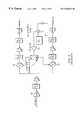
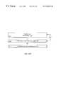
- a traditional receiver architecturemay employ superhetrodyne techniques as shown in FIG. 1 .
- a superhetrodyne architecturean incoming signal is frequency translated from its radio frequency (RF) to a lower intermediate frequency (IF).
- IFintermediate frequency
- Receiver designsmay have multiple IF stages. The reason for using such a frequency translation scheme is that circuit design at the lower IF frequency is much more manageable for signal processing. It is at these IF frequencies that the selectivity of the receiver is implemented, automatic gain control (AGC ) is introduced, etc.
- AGCautomatic gain control
- high Q filtersare also easier to implement at IF.
- High Q filtersare used to meet the selectivity and spurious rejection requirements dictated by wireless systems.
- SAWSurface acoustic wave
- ceramic technologyare typically used for the filtering depending on the frequency of operation.
- a direct conversion receiver architecturemay be used. This is shown in FIG. 2 . This scheme translates the incoming RF signal directly to baseband.
- the direct conversion architecturehas several advantages. First, there is no need for the high-Q filters required for traditional superhetrodyne architecture. Generally, all that is needed is a broadband RF filter which is used to reduce the dynamic range requirements of the RF down-converter. Second, there are a limited number of RF circuit blocks. Third, oscillators may be reduced to one. Fourth, it offers the smallest size solution since bulky off-chip filters are no longer required. Finally, because the low-pass channel filters are readily integrated, a fully integrated solution is achievable.
- wireless communications devicesuse high-frequency signals: 900 MHz to 1900 MHz for cellular phones and higher (up to 6 GHz) for other systems, such as wireless LANs.
- Radios for the so called “Bluetooth standard”(discussed below) operate in the unlicensed ISM band at 2.4 GHz. Signals at such frequencies are difficult to generate and control. They also have a tendency to interfere with each other, as they are easily coupled by parasitic properties present in all electronic components, including integrated circuits. In ICs, many of the undesirable parasitic effects result from the conductive silicon substrate on which the circuits are fabricated.
- LO leakagethere are several mechanisms through which LO leakage may occur. For example, there may be conducted paths between components. This occurs because there is limited isolation from the LO port of the mixers 12 to the RF port of the mixers 12 . There is also limited reverse isolation through the low-noise amplifying stages preceding the mixers 12 . A parasitic signal path for signals through the substrate, as well as a lateral signal path through the substrate, can also occur. In addition to the conducted path, there may also be radiated paths via the bond wires used to interconnect the circuit blocks to the outside world. The bond wires act as antennas and couple RF energy, such as that of the LO, to adjacent pins.
- the traditional solution for reducing the amount of signal that appears at the antenna portis to have the LO, i.e., the voltage controlled oscillator (VCO) 14 , at a different frequency than the incoming RF signal, as is indicated in FIG. 2 .
- VCOvoltage controlled oscillator
- This solutionrequires the use of dividers or multipliers 16 , as shown in FIG. 2, which adds additional circuitry.
- this solutiondoes not solve all of the problems of LO leakage associated with direct conversion receivers.
- IRinfrared
- Bluetoothis a global specification for wireless connectivity. It is based on a low-cost, short-range radio link that enables wireless communication of data and voice and facilitates protected ad hoc wireless connections for stationary and mobile communication environments.
- the proposal of Bluetoothis to offer a solution that yields rugged wireless connectivity.
- the Bluetooth standardwill be discussed herein as an example of a wireless communications standard, but it should be understood that the teachings of the present invention may be applied to any type of wireless communications and is not limited to the Bluetooth standard.
- Bluetooth Special Interest GroupSIG
- the Bluetooth specificationis being developed through the contributions of the members of the Bluetooth Special Interest Group (SIG).
- SIGBluetooth Special Interest Group
- the Bluetooth specificationis available from the Bluetooth Special Interest Group.
- Information regarding the Bluetooth standard, as well as procedures for obtaining the latest version of the Bluetooth specification,is available at the Internet web site http://www.bluetooth.com.
- Bluetooth technologyallows for the replacement of the many proprietary cables that connect one device to another with one universal short-range radio link. For instance, Bluetooth radio technology built into both the cellular telephone and the laptop would replace the cumbersome cable used today to connect a laptop to a cellular telephone. Printers, PDA's, desktops, fax machines, keyboards, joysticks and virtually any other digital device can be part of the Bluetooth system.
- Bluetooth radio technologyprovides a universal bridge to existing data networks, a peripheral interface, and a mechanism to form small private ad hoc groupings of connected devices away from fixed network infrastructures.
- the Bluetooth radiouses a fast acknowledgment and frequency hopping scheme to make the link robust.
- Bluetooth radio modulesavoid interference from other signals by hopping to a new frequency after transmitting or receiving a packet.
- the Bluetooth radiotypically hops faster and uses shorter packets. This makes the Bluetooth radio more robust than other systems.
- Short packages and fast hoppingalso limit the impact of domestic and professional microwave ovens.
- Use of Forward Error Correction (FEC)limits the impact of random noise on long-distance links.
- FECForward Error Correction
- Bluetooth radiosoperate in the unlicensed ISM band at 2.4 GHz.
- a frequency hop transceiveris applied to combat interference and fading.
- a shaped, binary FM modulationis applied to minimize transceiver complexity.
- the gross data rateis 1 Mb/s.
- a Time-Division Duplex schemeis used for full-duplex transmission.
- the Bluetooth baseband protocolis a combination of circuit and packet switching. Slots can be reserved for synchronous packets. Each packet is transmitted in a different hop frequency. A packet nominally covers a single slot, but can be extended to cover up to five slots.
- Bluetoothcan support an asynchronous data channel, up to three simultaneous synchronous voice channels, or a channel which simultaneously supports asynchronous data and synchronous voice. Each voice channel supports 64 kb/s synchronous (voice) link.
- the asynchronous channelcan support an asymmetric link of maximally 721 kb/s in either direction while permitting 57.6 kb/s in the return direction, or a 432.6 kb/s symmetric link.
- a piconetis a collection of devices connected via Bluetooth technology in an ad hoc fashion.
- a piconetstarts with two connected devices, such as a portable PC and cellular phone, and may grow to eight connected devices.
- All Bluetooth devicesare peer units and have identical implementations. Each unit has its own unique 48-bit address referred to as the Bluetooth device address. However, when establishing a piconet, one unit will act as a master and the other(s) as slave(s) for the duration of the piconet connection. Multiple independent and non-synchronized piconets form a scatternet.
- a master unitis the device in a piconet whose clock and hopping sequence are used to synchronize all other devices in the piconet. All devices in a piconet that are not the master are slave units.
- An Active Member addressis a 3-bit address to distinguish between units participating in the piconet.
- the master unitreceives the all zero Active Member for itself and thus there can be only seven active slaves in a piconet at any given time.
- Parked unitsare devices in a piconet which are synchronized but do not have Active Member addresses but can have 8-bit Passive Member addresses or be addressed with the full Bluetooth address.
- Active Member devices in a piconetcan enter power-saving modes in which device activity is lowered. This called a sniff and hold mode.
- the Bluetooth systemsupports both point-to-point and point-to-multi-point connections.
- piconetscan be established and linked together ad hoc, where each piconet is identified by a different frequency hopping sequence. All users participating on the same piconet are synchronized to this hopping sequence and the master's Bluetooth device address.
- the topologycan best be described as a multiple piconet structure.
- the full-duplex data rate within a multiple piconet structure with 10 fully-loaded, independent piconetsis more than 6 Mb/s. This is due to a data throughput reduction rate of less than 10% according to system simulations based on 0 dBm transmitting power (at the antenna).
- CVSDContinuous Variable Slope Delta Modulation
- the different functions in the Bluetooth systemare: a radio 20 , a link baseband controller (LC) 24 , a link manager (LM) 26 , software functions 28 , and a host processor or controller 30 .
- the radio 20is hardware that translates between binary bits and radio signals received and transmitted from an antenna 22 .
- the LC 24is hardware and/or software for performing the baseband processing and basic protocols close to the physical layer.
- the LM 26is software that carries out protocols such as link setup, authentication, link configuration, control, etc.
- the software functions 28may include configuration and diagnosis utility, device discovery, cable emulation, peripheral communication, audio communication and call control, object exchange for business cards and phone books, and networking protocol.
- the Bluetooth air interfaceis based on a nominal antenna power of 0 dBm.
- the air interfacecomplies with the FCC rules for the ISM band at power levels up to 0 dBm.
- Spectrum spreadinghas been added to facilitate optional operation at power levels up to 100 mW worldwide. Spectrum spreading is accomplished by frequency hopping in 79 hops displaced by 1 MHz, starting at 2.402 GHz and stopping at 2.480 GHz. Due to local regulations the bandwidth is reduced in Japan (2.471-2.497 GHz), France and Spain. This is handled by an internal software switch. For most functions, the maximum frequency hopping rate is 1600 hops/s. For paging functions, the hopping rate is 3200 hops/s.
- the nominal link rangeis 10 centimeters to 10 meters, but can be extended to more than 100 meters by increasing the transmit power.
- connection procedureis initiated by any of the devices which then becomes master.
- a connectionis made by a PAGE message if the address is already known, or by an INQUIRY message followed by a subsequent PAGE message if the address is unknown.
- the master unitIn the initial PAGE state, the master unit will send a train of 16 identical page messages on 16 different hop frequencies defined for the device to be paged (slave unit). If there is no response, the master transmits a train on the remaining 16 hop frequencies in the wake-up sequence. If the radio link is reliable, the maximum delay before the master reaches the slave is twice the wakeup period (2.56 seconds) while the average delay is half the wakeup period (0.64 seconds).
- the INQUIRY messageis typically used for finding Bluetooth devices, including public printers, fax machines and similar devices with an unknown address.
- the INQUIRY messageis very similar to the page message, but may require one additional train period to collect all the responses.
- a power saving modecan be used for connected units in a piconet if no data needs to be transmitted.
- the master unitcan put slave units into HOLD mode, where only an internal timer is running. Slave units can also demand to be put into HOLD mode. Data transfer restarts instantly when units transition out of HOLD mode.
- the HOLDis used when connecting several piconets or managing a low power device such as a temperature sensor.
- SNIFF modeTwo more low power modes are available, the SNIFF mode and the PARK mode.
- SNIFF modea slave device listens to the piconet at reduced rate, thus reducing its duty cycle.
- the SNIFF intervalis programmable and depends on the application.
- PARK modea device is still synchronized to the piconet but does not participate in the traffic. Parked devices have given up their Active Member address and occasionally listen to the traffic of the master to re-synchronize and check on broadcast messages.
- the SNIFF modehas the higher duty cycle, followed by the HOLD mode with a lower duty cycle, and finishing with the PARK mode with the lowest duty cycle.
- the link typedefines what type of packets can be used on a particular link.
- the Bluetooth baseband technologysupports two link types: Synchronous Connection Oriented (SCO) type (used primarily for voice), and Asynchronous Connectionless (ACL) type (used primarily for packet data).
- SCOSynchronous Connection Oriented
- ACLAsynchronous Connectionless
- Different master-slave pairs of the same piconetcan use different link types, and the link type may change arbitrarily during a session.
- TDDTime Division Duplex
- the SCO linkis symmetric and typically supports time-bounded voice traffic. SCO packets are transmitted at reserved slots. Once the connection is established, both master and slave units may send SCO packets without being polled.
- One SCO packet typeallows both voice and data transmission—with only the data portion being retransmitted when corrupted.
- the ACL linkis packet oriented and supports both symmetric and asymmetric traffic.
- the master unitcontrols the link bandwidth and decides how much piconet bandwidth is given to each slave, and the symmetry of the traffic. Slaves must be polled before they can transmit data.
- the ACL linkalso supports broadcast messages from the master to all slaves in the piconet.
- Bluetooth baseband controllersThere are three error-correction schemes defined for Bluetooth baseband controllers: 1/3 rate forward error correction code (FEC); 2/3 rate forward error correction code FEC; and Automatic repeat request (ARQ) scheme for data.
- FEC1/3 rate forward error correction code
- FEC2/3 rate forward error correction code
- ARQAutomatic repeat request
- the purpose of the FEC scheme on the data payloadis to reduce the number of retransmissions.
- FECcreates unnecessary overhead that reduces the throughput. Therefore, the packet definitions have been kept flexible as to whether or not to use FEC in the payload.
- the packet headeris always protected by a 1/3 rate FEC; it contains valuable link information and should survive bit errors.
- An unnumbered ARQ schemeis applied in which data transmitted in one slot is directly acknowledged by the recipient in the next slot. For a data transmission to be acknowledged both the header error check and the cyclic redundancy check must be okay; otherwise a negative acknowledge is returned.
- the Bluetooth basebandprovides user protection and information privacy mechanisms at the physical layer. Authentication and encryption are implemented in the same way in each Bluetooth device, appropriate for the ad hoc nature of the network. Connections may require a one-way, two-way, or no authentication. Authentication is based on a challenge-response algorithm. Authentication is a key component of any Bluetooth system, allowing the user to develop a domain of trust between a personal Bluetooth device, such as allowing only the owner's notebook computer to communicate through the owner's cellular telephone. Encryption is used to protect the privacy of the connection. Bluetooth uses a stream cipher well suited for a silicon implementation with secret key lengths of 8 to 128 bits. Key management is left to higher layer software.
- Bluetooth's security mechanismsprovide an appropriate level of protection for Bluetooth's short-range nature and use in a global environment. Users requiring stalwart protection are encouraged to use stronger security mechanisms available in network transport protocols and application programs.
- the modulator and demodulatorare typically implemented in a combination of the radio 20 and LC 24 .
- the hardware for the LC 24will typically be specific to the radio 20 being used.
- the LC 24is specific to the system since it implements system protocol functions. It is also specific to the type of modulation used in the system and it is also dependent upon the type of radio architecture implemented. At least some of this hardware will typically be integrated into a baseband IC performing LC 24 and possibly LM 26 functions as an application specific integrated circuit (ASIC).
- a demodulatorwill demodulate the signal that appears at the output of the radio receiver.
- the output from the demodulatoris raw data that is typically passed directly to the LC 24 for further processing to correct any errors and extract the payload.
- the output from the host processor 30is passed through Bluetooth Software Functions 28 and LM 26 to the LC 24 .
- the signalis data that has been formatted by the LC 24 into the appropriate structure with the addition of error correction, address bits, etc.
- This conventional implementationhas several disadvantages. Specifically, it requires a special ASIC with a processor to implement all of the Bluetooth functions, and the processor runs to perform all operations. All received data goes from the radio to the LC 24 over an external interface which will consume power and cause interference. The LC 24 has to perform frequency hopping by sending many commands to the radio. Finally, the LC 24 has to have many I/O lines into the radio for monitor and control. It would be desirable to have a more flexible way to implement the Bluetooth system, as well as a lower cost, lower power solution which conserved the resources of the host controller or microprocessor 30 .
- a conventional implementationwill typically include several discrete RF circuit components, which as discussed above, will result in the radio 20 having a large size and footprint, being expensive and power consuming.
- an improved radio designthat is a low cost, low power and small size solution could be used not only in cellular telephones, cordless telephones, etc., but also in implementing various wireless communications standards, specifications and/or protocols such as the Bluetooth standard. Furthermore, it would also be highly desirable to have an apparatus and method for wireless communications that could be used to efficiently implement various wireless communications standards, specifications and/or protocols, such as the Bluetooth standard, into a flexible, low cost, low power and small size solution.
- the present inventionprovides an apparatus for receiving signals.
- the apparatusincludes a low noise amplifier (LNA) configured to receive a radio frequency (RF) signal.
- An I/Q direct down converteris coupled to the LNA.
- the I/Q direct down converteris configured to split the RF signal into real and imaginary components and to down convert the real and imaginary components directly to baseband signals.
- a local oscillator (LO)is coupled to the I/Q direct down converter and is configured to drive the I/Q direct down converter.
- First and second filtersare coupled to the I/Q direct down converter.
- the first and second filtersare configured to filter the down converted real and imaginary components, respectively.
- First and second analog-to-digital converters (ADCs)are coupled to the first and second filters, respectively.
- the first and second ADCsare configured to convert the real and imaginary components into digital signals.
- the first and second ADCshave a dynamic range that is wide enough to convert the filtered, down converted real and imaginary components to digital signals without using variable gain on the filtered and down converted real and imaginary components.
- the present inventionalso provides an apparatus for receiving and transmitting signals.
- the apparatusincludes a local oscillator (LO), a direct conversion transmitter coupled to the LO that is configured to up-convert baseband signals directly to radio frequency (RF) for transmission, and a direct conversion receiver coupled to the LO that is configured to down-convert a received RF signal directly to baseband.
- the direct conversion receiverincludes an analog-to-digital converter (ADC) that is configured to convert the down-converted received RF signal into a digital signal.
- ADCanalog-to-digital converter
- the ADChas a dynamic range that is wide enough to convert the down-converted received RF signal to a digital signal without using variable gain on the down-converted received RF signal.
- the present inventionprovides an apparatus for use in wireless communications.
- the apparatusincludes a radio, a modem and a controller integrated onto a single integrated circuit (IC).
- the radiohas a receiver for receiving data and a transmitter for transmitting data.
- the modemis coupled to the radio and is configured to demodulate received data and modulate data for transmission.
- the controlleris coupled to the modem and includes a digital interface for external communications through which received data and data for transmission is sent, a connection state machine configured to accept commands through the digital interface and to respond to the commands by initiating a sequence, and a receive/transmit state machine configured to perform state control of the radio in response to the initiated sequence.
- the present inventionalso provides a method of performing wireless communications.
- the methodincludes receiving commands from an external processor through a digital interface where the digital interface is integrated onto a single integrated circuit (IC); initiating a sequence in circuitry included on the single IC in response to the received commands; performing state control of a radio that is integrated onto the single IC in response to the initiating sequence; and communicating data with the radio.
- ICintegrated circuit
- FIG. 1is a schematic diagram illustrating a conventional superhetrodyne receiver architecture.
- FIG. 2is a schematic diagram illustrating a conventional direct conversion receiver architecture.
- FIG. 3is a block diagram illustrating the different function blocks in the Bluetooth system.
- FIG. 4is a schematic diagram illustrating a direct conversion radio.
- FIG. 5is a schematic diagram illustrating a direct conversion radio in accordance with the present invention.
- FIG. 6is a schematic diagram illustrating the VCO/PLL shown in FIG. 5 .
- FIG. 7is a block diagram illustrating a direct conversion radio and digital processing circuitry in accordance with the present invention.
- FIGS. 8A and 8Bare isometric diagrams illustrating IC integration of the devices shown in FIGS. 5 and 7.
- FIG. 9is a flow diagram illustrating the operation of a DC offset cancellation scheme in accordance with the present invention.
- FIG. 10is a schematic diagram illustrating a direct conversion radio in accordance with the present invention.
- FIG. 11is a block diagram illustrating a direct conversion radio and digital processing circuitry in accordance with the present invention.
- FIG. 12is a schematic diagram illustrating an example of a coarse DC offset cancellation circuit.
- FIG. 13is a timing diagram illustrating an example of a DC calibration sequence.
- FIG. 14is a block diagram illustrating an architecture for wireless communications in accordance with the present invention.
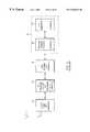
- FIGS. 15A and 15Bare block diagrams illustrating ways of interfacing the architecture shown in FIG. 14 with a host.
- FIGS. 16A, 16 B, and 16 Care block diagrams illustrating several ways of interfacing the architecture shown in FIG. 14 with a PDA.
- FIG. 17is a table illustrating trade-offs for the different external interfaces.
- FIGS. 18A, 18 B, 18 C and 18 Dare block diagrams illustrating several ways of interfacing the architecture shown in FIG. 14 with a PC.
- FIG. 19is a block diagram illustrating a way of interfacing the architecture shown in FIG. 14 with a cellphone.
- FIGS. 20A and 20Bare block diagrams illustrating two different types of internal interfaces which may be used with the architecture shown in FIG. 14 .
- FIG. 21is a table illustrating trade-offs for the different internal interfaces.
- FIG. 22is a block diagram illustrating the architecture for wireless communications shown in FIG. 14 in more detail.
- FIG. 23is a block diagram illustrating a radio interface which may be used for the radio.
- FIG. 24is a block diagram illustrating the modem shown in FIG. 14 in more detail.
- FIG. 25is a block diagram illustrating the FM detect and data slice block shown in FIG. 24 in more detail.
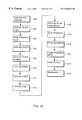
- FIG. 26is a block diagram illustrating the controller shown in FIG. 14 in more detail.
- FIGS. 27A, 27 B and 27 Care block diagrams illustrating three different types of interfaces that can be used on the controller shown in FIG. 26 .
- FIG. 28is a flow diagram illustrating the operation of the controller shown in FIG. 26 .
- FIGS. 29A, 29 B, 29 C, 29 D, 29 E, 29 F, 29 G and 29 Hare flow diagrams illustrating the operation of the controller shown in FIG. 26 .
- FIGS. 30A and 30Bare timing diagrams illustrating advantages of the use of the architecture for wireless communications shown in FIG. 14 .
- FIG. 31is a block diagram illustrating alternative applications of the architecture for wireless communications shown in FIG. 14 .
- FIG. 32is a schematic diagram illustrating an application of the architecture for wireless communications shown in FIG. 14 .
- FIG. 33is an isometric, cross-sectional view of the architecture for wireless communications shown in FIG. 14 integrated onto a single integrated circuit (IC).
- ICintegrated circuit
- FIG. 34is a cross-sectional view of semiconductor devices fabricated using a silicon-on-insulator (SOI) process technology.
- SOIsilicon-on-insulator
- FIG. 35is a flow diagram illustrating the process steps used to fabricate the semiconductor devices shown in FIG. 34 .
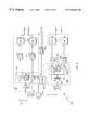
- the radio 100includes a direct down-conversion receiver 114 , a direct up-conversion transmitter 112 , a transmit/receive switch 124 , a VCO/PLL (phase locked loop) 116 , and an automatic gain control (AGC) control block 160 .
- AGCautomatic gain control
- the direct conversion radio 100has two functions. First, it takes a signal that appears at the output of the antenna 108 and down-converts it so that the signal can be further processed in the digital domain. This processing is done in the direct down-conversion receiver 114 and involves filtering the incoming signal and down-converting the signal to a much lower frequency, i.e. directly to baseband. The second function is a transmit function. This is done in the direct up-conversion transmitter 112 and involves up-converting and amplifying a modulated signal to the final frequency and power for transmission. Demodulation of the received signal, as well as modulation of the signal for transmission, may be provided by a modem which may either be external or on the same IC chip with the radio 100 as will be described below.
- the direct down-conversion receiver 114receives the RF input at the input of a low noise amplifier (LNA) 126 .
- the output of the LNA 126is fed into the inputs of two mixers 132 , 134 .
- the mixers 132 , 134 and the phase shifter 136cause the signal to be split into its complex coordinates.
- the quadrature (or 90°) phase shifter 136is driven by the PLL/VCO 116 .
- Automatic gain control by amplifiers 144 , 146is performed on the outputs of the mixers 132 , 134 , respectively.
- the outputs of the amplifiers 144 , 146are filtered by filters 152 , 154 , the outputs of which are amplified by variable gain amplifiers 148 , 150 . These signals are then converted to digital form by analog-to-digital converters (ADC) 156 , 158 .
- ADCanalog-to-digital converters
- variable gain amplifiers 148 , 150 and the control block 160form an automatic gain control (AGC) loop.
- AGCautomatic gain control
- the AGCsenses the level of the received signal and feeds it back to the variable gain amplifiers 148 , 150 in order to try to stabilize the signal level of the output of the variable gain amplifiers 148 , 150 .
- VSWRVoltage Standing Wave Ratio and is an impedance measure: a low VSWR means close to 50 ohms, and a high VSWR means not close to 50 ohms, i.e., either a very high impedance or a very low impedance, but not near 50 ohms.).
- variable gain amplifiers 148 , 150are especially problematic because as the gain varies it will modulate the already small, slowly varying low frequency signal that is supposed to be the DC level.
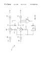
- the radio 200utilizes very wide dynamic range analog-to-digital converters (ADC) 226 , 228 which substantially reduces, or even eliminates, the need for AGC. This has many advantages which will be discussed below.
- ADCanalog-to-digital converters
- the direct conversion radio 200includes a direct down-conversion receiver 202 , a direct up-conversion transmitter 204 , a transmit/receive switch 206 , a VCO/PLL (phase locked loop) 208 , a transmit harmonic filter 210 , a receive band filter 212 , and a power control block 245 .
- the receiver 202receives the RF input at the input of a low noise amplifier (LNA) 214 , from the filter 212 .
- the output of the LNA 214is fed into the input of an I/Q direct down converter 215 .
- the I/Q direct down converter 215is configured to split the RF signal into real and imaginary components and to down convert the real and imaginary components directly to baseband signals.
- the mixers 216 , 218 and the quadrature (or 90°) phase shifter 220cause the signal to be split into its complex coordinates.
- the phase shifter 220is driven by the PLL/VCO 208 , i.e., the local oscillator 208 .
- the outputs of mixers 216 , 218are filtered by filters 222 , 224 , which are configured to filter the down converted real and imaginary components.
- the outputs of the filters 222 , 224are converted to digital form by 115 large dynamic range ADCs 226 , 228 , respectively.
- the direct up-conversion transmitter 204receives modulated digital data to be transmitted from a modem (not shown) at the inputs of the digital-to-analog converters (DAC) 230 , 232 .
- the outputs of the DACs 230 , 232are filtered by the filters 234 , 236 , respectively, the outputs of which are fed into the direct up-converter 237 .
- the phase shifter 242 and the mixers 238 , 240up-convert the signal which is then driven by the driver 244 .
- the output of the driver 244is filtered by the filter 210 . Referring to FIG.
- the PLL/VCO 208includes a voltage controlled oscillator (VCO) 248 , a phase locked loop (PLL) 250 , and an amplifier 252 .
- VCOvoltage controlled oscillator
- PLLphase locked loop
- the VCO 248includes a frequency control port 247 and an output port 249 .
- the direct conversion radio 200takes advantage of the larger dynamic range in the ADCs 226 , 228 .
- ADCs with wide dynamic rangeare typically of the delta-sigma or pipelined variety. Either of these varieties of ADCs, such as delta-sigma or sigma-delta converters, or any other ADCs having wide dynamic range or which are considered high resolution, such as those used in audio technologies, may be used in accordance with the present invention.
- the overall gain in the receiver 202can be kept relatively low. Furthermore, there is little or no gain at baseband either in the mixers 216 , 218 or the filters 222 , 224 .
- the DC offset from the mixers 216 , 218is not amplified, which means the ADCs 226 , 228 will not be overloaded by the DC offset.
- analog cancellation of the DC offset from the mixers 216 , 218is either not necessary, or the need for such cancellation is substantially reduced.
- excess gainis eliminated.
- AGCautomatic gain control
- the ADCs 226 , 228Due to the large dynamic range in the ADCs 226 , 228 , automatic gain control (AGC) is not necessary and can be eliminated or substantially eliminated in the radio 200 . This is possible because all or substantially all of the dynamic range can be handled by the ADCs 226 , 228 , with the possible exception of a switchable gain stage (e.g., a low noise amplifier). In this scenario, there may be no base band in the AGC. Any AGC that is used occurs at RF and is digital AGC, and so it can be controlled by a digital loop. Such digital loop can perform significant interpretation and intelligence before it makes the decision, which cannot be done with a traditional analog or pseudo analog loop. In any event, because the only gain control is in the RF, it has no impact on the DC offset. Therefore, by eliminating AGC, the variable gain amplifiers have been eliminated, which means the DC offset will be almost constant and will not be modulated.
- AGCcan be reduced to two settings due to the large dynamic range in the ADCs 226 , 228 .
- the receiver's base-band stagestypically remain linear throughout the dynamic range of the receiver.
- stages 222 , 224 , 226 , 228will compress.
- a gain reduction in the mixers 216 , 218ensures that these stages stay linear.
- a digital control signalforms the closed loop control for the AGC. The digital control sets mixers 216 , 218 in either a high or low gain setting depending on the expected signal level.
- the use of the large dynamic range ADCs 226 , 228not only allows elimination of variable gain, it also allows most of the filtering to be done in the digital domain, which has a number of advantages.
- One advantageis that in the digital domain there is much better control of the frequency. The corner frequencies do not vary with process and temperature.
- Another advantageis that there is potentially more dynamic range.
- Yet another advantageis that it can be programmable so that the bands can be changed.
- the ability to do the filtering in the digital domainallows the filtering to be done on-chip with the radio and eliminates the conventional practice of going off-chip to discrete filters.
- the conventional practice of going off-chip to discrete filtershas the disadvantage that it creates opportunities for noise and interference to be picked up off the main board, let alone requires more physical space.
- ADCsare considered to have a wide dynamic range or are of high resolution if they have a bit width wider than or equal to approximately twelve (12) bits or have greater than or equal to an approximately 74 dB range.
- ADCs having a bit width less than ten (10) bitsare generally considered to be low resolution. Therefore, the ADCs 226 , 228 have a dynamic range that is wide enough to convert the filtered, down converted real and imaginary components of the received RF signal to digital signals without using variable gain control (i.e., AGC).
- AGCvariable gain control
- ADCs with wide dynamic rangemay be of the delta-sigma variety.
- a delta-sigma modulator(or converter), also referred to as sigma-delta modulators, converts a signal amplitude into digital data.
- An input signal at a given frequency f Ois oversampled, that is, sampled at a rate f S much higher than the Nyquist rate, f S >>2f O .
- the delta-sigma modulatoris over-sampled, and preferably very highly over-sampled.
- the sample rate of the delta-sigma modulatormay be chosen substantially near the carrier frequency of the incoming RF signal.
- a delta-sigma modulatoremploys coarse quantization, filtering and feedback, such that the output is only one (or a few) bits wide, while the amount of quantization energy that lies in the desired frequency band is relatively small (i.e., high resolution).
- Post filteringis employed after the delta-sigma modulator to remove the out-of-band quantization energy.
- a 32 MHz, second order 4-bit delta-sigma modulatorthat includes 13-bits of signal resolution in the 0-500 KHz band may be employed in the present invention.
- U.S. Pat. No. 5,684,482 entitled “Spectral Shaping of Circuit Errors in Digital-to-Analog Converters”is hereby fully incorporated into the present application by reference. The teachings of this patent may be used in the present invention.
- AGCelimination of AGC also has the advantage of eliminating the problem of fading, a classic problem in radios that use AGC. Specifically, when the radio is receiving a strong signal, the AGC turns all of the gain down in order to prevent that signal from overloading the amplifier. The strong signal, however, can quickly drop and becomes very weak, possibly because the radio is moved. In this scenario the AGC may not be able to respond fast enough to turn the gain back up for the weak signal, resulting in the signal actually being lost. With cellular telephones this is known as a “drop-out”. By eliminating the AGC in the radio 200 , however, this type of fading is eliminated. The total drop-out phenomenon, i.e., where there is just not enough signal at all, is still a problem with all radios.
- the radio 200may be referred to herein as the “radio front-end” 200 .
- the ADCs 226 , 228 and the DACs 230 , 232are shown as part of the digital processing stage 300 rather than the radio 200 . It should be understood that the ADCs 226 , 228 and the DACs 230 , 232 may be considered as part of the radio 200 as described above or as part of the digital processing stage 300 in accordance with the present invention.
- the digital processing stage 300includes decimation filters 302 , 304 , a digital receive filter 306 , and a digital transmit filter 308 . Furthermore, the digital processing stage 300 includes a DC offset cancellation block 310 . As will be discussed below, the decimation filter 302 and the digital receive filter 306 may be combined into one filter, and the decimation filter 304 and the digital transmit filter 308 may be combined into one filter.
- the radio 200 and the digital processing stage 300combine direct RF conversion and delta-sigma data conversion in a unique way that produces a baseband digital receive signal that is further processed in the digital domain.
- the resultis a “software radio” or a “software defined radio” or a “digital radio”, i.e., a radio that can be changed or adapted to whatever standard is required simply by changing digital circuits.
- the approach described herein for such a software radiois a low cost, small size and low power consumption solution. The operation of the digital processing stage 300 will be discussed below.
- the radio 200alone may be integrated onto a single IC chip as shown in FIG. 8A, or that the radio 200 along with the digital processing stage 300 may be integrated onto a single IC chip as shown in FIG. 8B, or that the radio 200 , digital processing stage 300 , and other components may be integrated onto a single IC chip.
- FIG. 8Athe radio 200 alone may be integrated onto a single IC chip as shown in FIG. 8A, or that the radio 200 along with the digital processing stage 300 may be integrated onto a single IC chip as shown in FIG. 8B, or that the radio 200 , digital processing stage 300 , and other components may be integrated onto a single IC chip.
- An example of this later scenariowill be discussed below with respect to the integration of a radio, modem and controller onto a single IC chip. It should be understood, however, that such integration is not a requirement of the present invention.
- the radio 200is integrated onto an IC chip, it has been found herein that the LO leakage problems discussed above with respect to the direct conversion receiver shown in FIG. 2 can be overcome, or at least significantly reduced.
- One factor that has contributed to the LO leakage problems being overcomeis the selection of the fabrication process used to fabricate the transistors and other devices that form the circuit components which make up the radio 200 .
- silicon-on-insulator (SOI) BiCMOS technologyhas many characteristics that are preferable to alternative technologies. There are also several features that make it particularly well-suited to RF applications, such as the radio 200 .
- SOIsilicon-on-insulator
- an insulating layer 320separates circuit devices from the solid silicon substrate 322 .
- a trench isolation structuremay also be used which provides a lateral barrier between circuit elements. These features isolate signals and minimize the undesired coupling that would otherwise limit performance. Because parasitic effects also limit the speed at which a circuit can operate, ICs made with SOI offer exceptional high-frequency operation while minimizing power dissipation.
- the isolating properties of the SOI technologyallow more functions to be packed into a single die. These characteristics translate into advantages in performance, battery life, and size for the end product.
- the radio 200(and the digital processing stage 300 ) is preferably formed on an SOI substrate, using well-known SOI BiCMOS IC manufacturing processes.
- An insulating layerseparates circuit devices from a solid silicon substrate.
- the advantages of SOI BiCMOS process technologyinclude greater signal isolation, higher speed devices with lower power consumption, and dense digital CMOS logic.
- the circuitry of the present inventionis preferably implemented in an SOI BiCMOS process technology that uses bonded wafers (“bonded SOI”). Bonded SOI processes are well-known to those of ordinary skill in the art and are believed to be currently available. Exemplary SOI BiCMOS process technologies that may be used to implement the present invention are described in U.S. Pat. No.
- the radio 200When the radio 200 is implemented in SOI, many of the leakage problems described in connection with the direct conversion receiver of FIG. 2 are significantly reduced due to the characteristics of the SOI process.
- the circuitryin the receiver 202 , if the circuit is fabricated using SOI, the circuitry will be isolated from the bulk substrate by a thin layer of SiO 2 . With the additional use of a high resistivity substrate, minimal parasitic capacitance will be associated with the circuit elements. This will minimize the parasitic signal paths (conductive paths) that result from the capacitances associated with the various circuit elements, which in turn, will significantly improve isolation from the LO port of the mixers 216 , 218 to the RF port of the mixers 216 , 218 .
- the substrateis preferably formed of a high resistivity (or high Z) material having a high ohm per centimeter rating, such as for example, a 1K ⁇ per centimeter substrate. While a 1K ⁇ per centimeter substrate performs very well, it should be understood that a substrate is considered herein to be a high resistivity (or high Z) substrate if it has an ohm per centimeter rating above approximately 100 ⁇ per centimeter.
- lateral signal paths through the substratethese may be reduced using trench isolation between adjacent blocks.
- An example of an isolation scheme that has been found to work particularly well in implementing the radio 200 on a single IC chip and which may be used in the present inventionis the isolation scheme described in copending U.S. patent application Ser. No. 09/255,747, filed Feb. 23, 1999, entitled “TRENCH ISOLATED GUARD RING REGION FOR PROVIDING RF ISOLATION”, invented by James D. Seefeldt, and commonly assigned herewith, the full disclosure of which is hereby incorporated into the present application by reference.
- the properties of SOIare such that the circuit blocks are fabricated on top of a high resistance layer of SiO 2 .
- the common substrateis high resistivity, then the path through the substrate is very high impedance. This means there is a high level of isolation between the LNA 214 and the LO port of the mixers 216 , 218 .
- the amount of LO signal that appears at the output of the receiver 202can be minimized, thus reducing the problem of LO leakage through conducted and substrate paths.
- the bond wires of an IC packagecan couple RF energy (such as that of the LO) to adjacent I/O pins.
- RF energysuch as that of the LO
- the LO signalis only present on the chip itself.
- VCOvoltage controlled oscillator
- One challenge in fully integrating the LO circuitryis the design of the voltage controlled oscillator (VCO) 248 . It is preferable that the LO signal be spectrally clean to meet the requirements of a wireless system.
- the VCO 248 phase noiseis an important part of this noise profile.
- the spectral purity of the VCO 248is dependent on the Q of the resonator (or “tank”), i.e., the inductor 254 and the capacitor 256 , used in the design.
- the Q of the inductor used in the resonatorgenerally dominates the Q of the resonator. The challenge therefore becomes the design of integrated inductors with high enough Q. If a spiral inductor is fabricated on a high resistivity substrate (as described above), the Q can be made high enough to implement a spectrally clean VCO 248 and therefore a suitable LO for use in direct conversion applications.
- SOI with a high resistivity substratehelps to allow the full integration of the LO since it permits high Q inductors to be fabricated in accordance with the above-referenced U.S. patent application. This results in the LO signal being substantially only present on chip and the radiated path for LO-leakage is minimized. Additional detail regarding SOI processes, as well as advantages that result from the use of SOI, will be discussed below.
- VCO 248 of the receiver 202Because of the improved isolation and reduced LO leakage which can result from the selection of device fabrication processes, such as SOI process technology, it becomes practical to operate the VCO 248 of the receiver 202 at the same or substantially the same frequency as the incoming RF signal received by the LNA 214 .
- the traditional solution for reducing the amount of signal that appears at the antenna port in direct conversion receiversis to have the voltage controlled oscillator (VCO) at a different frequency than the incoming RF signal.
- VCOvoltage controlled oscillator
- VCO 248Operating the VCO 248 at the same frequency as the incoming RF signal has the advantage of eliminating the need for multiplier or divider circuitry that would normally be associated with the amplifier 252 . Eliminating this additional circuitry that is traditionally used results in a lower current, smaller and lower cost solution.
- the radio 200is integrated onto an IC chip a very small size, low cost and low current solution will result.
- all of the receiver functionality, including the channel filters,may be integrated.
- the LNA 214may have a separate power control. This allows the LNA 214 to be switched off independently.
- the digital processing stage 300 shown in FIG. 7includes decimation filters 302 , 304 , a digital receive filter 306 , a digital transmit filter 308 , and a DC offset cancellation block 310 .
- the decimation filter 302 and the digital receive filter 306may be left as separate filters or combined into one digital filter.
- the purpose of the DC offset cancellation block 310is to remove the DC offset with digital processing directly. This is possible because static DC offsets can be sampled, stored and then canceled relatively easily compared to variable DC offsets. Even variable DC offsets can be canceled. Specifically, this is done by dropping the LO 248 's signal to the sensitivity level of the radio 200 which causes the randomness of the DC offset to become smaller than the sensitivity of the radio 200 .
- the signalmust be brought down to on the order of ⁇ 100 dBM. While this has been difficult to do with conventional radios, the fully integrated VCO 248 and the isolation structures used with SOI in the radio 200 makes it possible. This is because of the higher Q inductors which result in low phase noise VCOs with fully integrated tanks (i.e., LC resonators) and the isolation structures that prevent energy from leaking back to the LNA 214 .
- the DC offset cancellation block 310removes the varying DC component by taking advantage of the fact that in some systems, such as TDMA and TDD systems, there are periods of time when the transmitter 204 will not be turned on and when the receiver 202 will not be turned on. During these periods of time the radio 200 is basically inactive and both the transmitter 204 and the receiver 202 are inactive. So, during these inactive periods, the DC offset cancellation block 310 turns off the LNA 214 and measures the true DC offset.
- the output impedance of the LNA 214does not significantly change when it is turned off.
- the output impedance of the LNA 214does not significantly change because of the SOI process by which the device is made and the high isolation techniques employed.
- the semiconductor process and isolation techniquesenable the LNA 214 to operate more like a “perfect” device. This means that while the LNA 214 is turned off, it is possible to get a nearly true reading of the actual DC offset generated by the internal effective circuit. This allows the DC offset cancellation block 310 to make a refined correction to the DC offset or component that is leaking through, thus eliminating the DC component.
- a DC offset cancellation processbegins in steps 324 and 326 where it is determined whether or not the receiver 202 and the transmitter 204 are in an idle, inactive period. If so, the DC offset cancellation block 310 turns off the LNA 214 in step 328 . Instep 330 the DC offset is measured while the LNA 214 is turned off, and in step 332 the DC offset cancellation block 310 corrects the DC offset based on the measured DC offset.
- FIG. 10there is illustrated another radio front-end 350 in accordance with the present invention.
- FIG. 11illustrates the radio front-end 350 and a digital processing stage 362 .
- the ADCs 226 , 228 and the DACs 230 , 232are shown as part of the digital processing stage 362 rather than the radio front-end 350 . It should be understood that the ADCs 226 , 228 and the DACs 230 , 232 may be considered as part of the radio front-end 350 or as part of the digital processing stage 362 in accordance with the present invention.
- the radio 350 and the digital processing stage 362utilize another type of DC offset correction in accordance with the present invention.
- the receiver 351 of the radio 350includes coarse DC offset cancellation circuits 352 , 354
- the digital processing stage 362includes a fine DC offset cancellation stage 360 .
- the coarse DC offset cancellation circuits 352 , 354provide analog DC offset cancellation
- the fine DC offset cancellation stage 360provides a digital DC offset cancellation. This combination of analog and digital DC offset cancellation is particularly advantageous in direct conversion radios and in the context of TDMA and TDD systems.
- the coarse DC offset cancellation circuits 352 , 354 and the fine DC offset cancellation stage 360provide two DC offset corrections.
- the first correctionis performed by the DC offset cancellation circuits 352 , 354 and is an analog correction that is done in a mixed mode domain. In other words, this correction is performed just after the I/Q direct down converter 215 .
- FIG. 12illustrates the DC offset cancellation circuit 352 in further detail.
- the technique that the circuit 352 implementsis successive approximation analog-to-digital conversion. Specifically, a differential input signal is received at inputs 364 , 365 .
- the current sources 366 , 367provide current inputs to the summation blocks 368 , 369 , respectively.
- the summation blocks 368 , 369 output nodes 376 , 378are connected via a resistor R, which for example may have a value of 20 K ⁇ .
- the output nodes 376 , 378are used as the inputs of a comparator 372 , the output of which is fed into a DAC 373 .
- the output of the DAC 373is fed through current sources 375 , 374 and then into the summation blocks 368 , 369 , respectively.
- the DAC 373which facilitates the canceling of the DC offset.
- the comparator 372measures the difference in the voltage between nodes 376 , 378 and generates a digital output.
- the DAC 373takes this digital output and provides a feedback current to the summation blocks 368 , 369 .
- the feedback currentattempts to drive the error between nodes 376 , 378 to zero.
- the error at the nodes 376 , 378is a voltage.
- the voltage difference at nodes 376 , 378is driven to zero which results in the DC offset being canceled.
- the successive approximation techniqueprovides only a course DC offset cancellation. This is because to increase the resolution of the successive approximation of the ADC and DAC, the bit width of the data converters needs to be very large. Therefore, the resolution is basically limited by the matching of the DAC 373 .
- the DAC 373may be either 6 bits or 8 bits.
- the coarse DC offset cancellation circuits 352 , 354provide DC offset cancellation for the DC offsets of the mixers 216 , 218 .
- the specific resolution of the coarse correction made by the DC offset cancellation circuits 352 , 354is not critical. This is because the correction is done at the output of the mixers 216 , 218 so that the cascading DC offsets will not cause later stages to saturate. However, any DC offset after the mixers 216 , 218 will still be seen in the digital domain. For example, even the ADCs 226 , 228 can have a DC offset. Therefore, it is advantageous to perform a fine DC offset correction in the digital domain.
- This fine DC offset correctionis performed by the fine DC offset cancellation stage 360 .
- the fine DC offset cancellation stage 360provides a second DC offset correction.
- FIG. 13illustrates the steps and timing for each event that occurs during and before a receive (RX) burst in this example. This example assumes that the receiver is out of sleep mode and that a 32 MHz clock and analog regulators are up and settled.
- the example operationbegins with a VCO tune period that is approximately 220 ⁇ sec long.
- the VCO tune periodoccurs between each frame of transmit and receive and is basically a dead period.
- One purpose of this dead periodis to allow the synthesizer to settle because it is changing frequencies.
- the LNA 214is turned off as indicated at 380 .
- the first step indicated at 381occurs 35 ⁇ secs before the receiver burst and is the coarse DC calibration. This is a hardware calibration undertaken by circuits 352 , 354 described above. The actual time it takes to do the calibration is approximately 8 ⁇ secs. Approximately 14 ⁇ secs after initiating the coarse DC calibration, the second DC calibration occurs as indicated at 382 . This is the fine DC calibration performed by block 360 . The signal “dccal” is sent to the digital demodulation section (described below). During the second or fine
- the DC offset due to the intrinsic circuitryis sampled.
- the sampled DC offsetis averaged over some finite period of time, normally at least 10 microseconds.
- the DC offsetmay be averaged over 32 microseconds.
- the calculated average DC offsetis subtracted out from all of the data of the next frame. This process occurs in the fine DC offset cancellation stage 360 after the decimation filter 356 . It is typically a slow process and is done at a very high resolution.
- the decimation filter 356provides the high resolution.
- Each of the trigger pulsesis 1 ⁇ sec long as indicated at 383 , and the coarse correction circuits 352 , 354 are ⁇ ve edge sensitive.
- the leading edge of the 1 ⁇ sec trigger pulseinitiates the second DC calibration.
- the LNA 214is powered up 5 secs before the RX burst is expected as indicated at 384 . This allows time for the receiver to settle after this disturbance.
- the actual length of the RX Burst, X ⁇ secsdepends on the type of burst to be received.
- the TX/RX switch signal 385(shown as a dotted line) is not required in the example described, it may be used if the DC calibration requires more isolation from the antenna than is provided when the LNA 214 is turned off. Under such circumstances the TX/RX switch will go into TX mode during the calibration period.
- the decimation filters 302 , 304 , the digital receive filter 306 , and the digital transmit filter 308 of the digital processing stage 300have been combined in accordance with the present invention. Specifically, the decimation filter 302 and the digital receive filter 306 have been implemented in one combined filter 356 , and the decimation filter 304 and the digital transmit filter 308 have been implemented in one combined filter 358 .
- the radio 200may be implemented in many different ways with any one or more of several optional features. For example, multiple power modes may be included which allow each section of the radio 200 to be powered up and down independently.
- the reference oscillator crystal and the low-power oscillator crystalmay be located external to the radio 200 .
- An external amplifiermay be added to allow operation where extended range capability is required. In the scenario where the UHF PLL/VCO 208 is utilized, no external VCO resonator components are required.
- the dc power to each stage in the radio 200may be controlled separately.
- Various on-chip switchesmay be added to control the dc power to the reference oscillator, the transmitter 204 , the PLL/VCO 208 , the receiver 202 and the LNA 214 .
- the RMCThe RMC
- an architecture 1100in accordance with the present invention.
- the architecture 1100is particularly useful for implementing wireless communications.
- the architecture 1100may be used to efficiently implement the radio 20 and the link baseband controller 24 layer of the Bluetooth specification described above, as well as some portions of the link manager 26 layer, such as for example the low power mode protocols and initial call setup.
- Implementing portions of the link manager 26adds functionality which substantially improves the performance of the Bluetooth system.
- the improved performanceis due, at least in part, to the advantages of the architecture 1100 , which include lower current and power, lower cost, lower interference, smaller size and footprint, and the ability to be implemented with multiple product platforms.
- the link manager 26 layerThere are two categories of protocol actions in the link manager 26 layer that are implemented by the architecture 1100 .
- the firstis rapid and tightly time constrained actions.
- the Page, Page Scan, Inquiry and Inquiry Scanare implemented in the connection state machine (discussed below) of the controller 1106 .
- Implementation of these functions in the controller 1106relieves the host or external processor from these tasks. This saves power and reduces the requirements of the external processor.
- the second category of protocolsis repetitive transmission and monitoring actions of master and parked slave. By implementing this action in the architecture 1100 the external processor can remain powered down until something addressed to the unit occurs. This also saves power.
- the controller 1106includes a Rx/Tx state machine, which implements link controller actions, and a connection state machine, which implements protocol actions.
- the other portions of the link manager 26 layer, as well as the higher layers of the Bluetooth specification,may be implemented in an external processor or the host.
- the architecture 1100will run autonomously according to commands and state machine design until one of several events occur at which time the controller 1106 will interrupt or otherwise communicate with the host to indicate completion or abnormal ending of the commanded actions.
- the higher layers of the Bluetooth specificationare partitioned between software and hardware implementation. The choice of hardware versus software implementation may be made, for example, upon whether the frequency of the signal being processed is high, or the function is repetitive in all conditions. If the frequency is high and the function predictable, the functions may be implemented in hardware. Mode dependent functions such as Logical Link control may be implemented in software.
- the architecture 1100is particularly useful for implementing the Bluetooth specification, it should be well understood that the architecture 1100 may also be used, in accordance with the present invention, to implement other types of wireless communications standards, specifications and/or protocols. Examples of other protocols that the architecture 1100 could be used to implement are Home RF, IEEE 802.11, etc. There are several standards in the ISM frequency band, and it is believed that Japan is reviewing their own requirements. Thus, the architecture 1100 may be used to implement many different types of wireless systems in the general ISM frequency band in addition to the Bluetooth standard. Whether or not it is used to implement the Bluetooth specification, the architecture 1100 may be used in cellular handsets, personal computer (PC) peripheral cable replacement, personal digital assistants (PDA), palmtop computers, personal organizers, cordless telephones, cordless headsets, etc.
- PCpersonal computer
- PDApersonal digital assistants
- the architecture 100generally includes a radio 1102 , a modem 1104 , and a controller 1106 . Because of its radio (R), modem (M), controller (C) architecture, the architecture 1100 may at times be referred to herein as the RMC 1100 .
- the radio 1102includes an antenna interface for connection to an antenna 1108 .
- the controller 1106includes a digital interface for communication with external devices. Control of the radio 1102 is provided by the modem 1104 and controller 1106 as described herein.
- the radio 1102may be a 2.4 GHz radio transceiver
- the modem 1104may be a 1 Mbps Gaussian Filtered Frequency Shift Keying (GFSK) modem
- the controller 1106may handle time-critical packet processing and protocols.
- the modem 1104 and the controller 1106may be used to implement the timing, frequency hopping, framing, packets, flow control, error detection and correction, and encryption specified in the Bluetooth specification.
- the modem 1104 and the controller 1106can fully implement the baseband or link control layer in the Bluetooth specification.
- the architecture 1100may be used to implement wireless communications in multiple frequency bands in accordance with the present invention and is not limited to 2.4 GHz.
- the architecture 1100may be used for, and the teachings of the present invention may be applied to, wireless communications devices using high-frequency signals such as 900 MHz to 1900 MHz for cellular phones and higher frequencies (up to 6 GHz) for other systems such as wireless local area networks (LANs), as well as any other frequency in the ISM band.
- high-frequency signalssuch as 900 MHz to 1900 MHz for cellular phones and higher frequencies (up to 6 GHz) for other systems such as wireless local area networks (LANs), as well as any other frequency in the ISM band.
- LANswireless local area networks
- the architecture 1100may be used to implement the Bluetooth system with a host microprocessor 1110 in a variety of ways. Referring to FIG. 15A, the architecture 1100 may be connected directly to the host 1110 . Referring to FIG. 15B, the architecture 1100 may be connected to a baseband controller processor 1109 , where the baseband controller 1109 is connected to the host 1110 . An advantage of using the baseband controller 1109 is that it can run software that implements the remaining Bluetooth specific tasks not handled by the architecture 1100 without involvement of the host 1110 . The baseband controller 1109 may be implemented with virtually any commercially available generic processor.
- the architecture 1100may be interfaced with PDAs, PCs and cell phones in a variety of ways.
- External interfacesmay include, for example, RS232C, CompactFlash, Improved CompactFlash, universal serial bus (USB), PCI, and PCMCIA.
- Internal interfacesmay include a serial port interface and a parallel interface.
- FIGS. 16A, 16 B and 16 Cshow several ways of interfacing the architecture 1100 with a palm PC 1111 .
- FIG. 16Ashows that RS232C may be used to interface with the BC 1109 (e.g., a cradle port interface).
- FIG. 16Bshows that CompactFlash may be used to interface with the BC 1109 .
- FIG. 16Cshows that CompactFlash may be used to interface directly to the architecture 1100 (an improved CompactFlash interface).
- FIG. 17illustrates some of the external interface tradeoffs.
- FIGS. 18A, 18 B, 18 C and 18 Dshow several ways of interfacing the architecture 1100 with a PC 1113 .
- FIG. 18Ashows that RS232C may be used to interface with the BC 1109 .
- FIG. 18Bshows that universal serial bus (USB) may be used to interface with the BC 1109 .
- FIG. 18Cshows that PCI may be used to interface with the BC 1109 .
- FIG. 18Dshows that PCMCIA (PC card interface) may be used to interface directly with the architecture 1100 .
- PCMCIAPC card interface
- FIG. 19illustrates one way in which the architecture 1100 may be interfaced to a cell phone 1115 .
- many cell phone OEMsuse a different interface. Some are similar to RS-232, and some are proprietary. In such a scenario, the proprietary serial interface may be used.
- FIGS. 20A and 20Billustrate internal interfaces options. Specifically, the interface is part of the controller 1106 which will be discussed in more detail below.
- the interfacemay be a serial interface as shown in FIG. 20 A.
- the serial interfacemay be a 4-Mbps synchronous serial interface (SSI).
- the interfacemay be a parallel interface as is shown in FIG. 20 B.
- the parallel interfacemay be an 8-bit parallel interface.
- the architecture 1100may include one or both of the serial and parallel interfaces.
- the host 1117may be, for example, a cellphone, PC, PPC, HPC, PC peripheral, cordless phone, headset, etc.
- FIG. 21illustrates some of the internal interface tradeoffs.
- the interfacefacilitates communication, such as exchange commands and data, with the interface of the BC or host to implement the higher layers of the Bluetooth protocol.
- the architecture 1100may be integrated onto a single integrated circuit (IC) chip (as is shown, for example, in FIG. 33 ).
- the architecture 1100may, for example, be integrated onto a single monolithic integrated circuit.
- the architecture 1100will provide a fully integrated radio transceiver, modem and baseband controller on a single chip. No external VCO or channel filter components will be required.
- integration of the architecture 1100 onto a single IC chipis not a requirement of the present invention. Indeed, the architecture 1100 may be implemented with discrete circuit components, as a module, with more than one IC chip, etc., all in accordance with the present invention.
- the radio 1102may be implemented in many different ways in accordance with the present invention.
- the radio 1102will generally include a transmitter 1112 , a receiver 1114 , and a UHF phase locked loop voltage controlled oscillator (PLL/VCO) 1116 .
- the transmitter 1112 and receiver 1114may be implemented using superhetrodyne techniques, such as is shown in FIG. 1 .
- the receiver's IFmay either be very high or very low in frequency.
- the transmitter 1112 and receiver 1114may be implemented using direct conversion techniques, such as is shown in FIG. 2 .
- FIG. 23illustrates a radio interface 1101 for interfacing the radio 1102 to the modem 1104 .
- the interfaceis set up for interfacing to the radio 100 , i.e., all of the components shown in the radio interface 1101 are also shown as part of the radio 100 , such as for example, the ADCs 156 , 158 and DACs 162 , 164 .
- the transmitted signalmay be GFSK modulated data that is amplified within the architecture 1100 to an output power of +3 dBm.
- Power controlmay also be implemented in the architecture 1100 , for example, by providing 30 dB of power control range. This allows the overall power efficiency of the architecture 1100 to be maximized.
- the architecture 100may be used with only one regulator.
- the 32 kHz low-power oscillator and associated circuitrymay be powered separately from an external power source. This allows the architecture 1100 and the host controller/microprocessor 1110 to be put into a sleep state during extended periods of inactivity.
- the modem 1104includes a demodulator 1196 for demodulating received data and a modulator 1198 for modulating data to be transmitted.
- the modem 1104is capable of performing GFSK modulation and demodulation, frame timing recovery, and frequency hop control.
- FIG. 24illustrates the modem 1104 in more detail.
- the modem 1104is partitioned into several blocks, which in turn, give rise to several advantages.
- the general functions of each of the blocks in the modem 1104are as follows.
- the FM detect and data slice block 1200receives the received data from the radio 1102 and performs the frequency to amplitude conversion and 1/0 bit decision functions.
- the symbol synchronization block 1202performs the symbol timing recovery function.
- the frame detect block 1204performs the frame header decision function and transfers the received data to the controller 1106 .
- the frequency hopping (FH) sequencer block 1206performs the frequency hop number generator function.
- the synthesizer programmer block 1208programs the radio 1102 to the next frequency.
- the radio control block 1210manages the various power modes.
- the burst timing and control block 1212receives control information and generates clocks for burst events.
- the GFSK Modulator 1214receives and maps TX data to the modulation waveform.
- the sliding correlator block 1216identifies received packets that are addressed to its own unit and immediately discards received packets that are addressed to a different unit.
- FIG. 25illustrates the FM detect and data slice block 1200 in further detail.
- the FM detect and data slice block 1200may include a DC offset correction stage 1201 , an FM detect stage 1203 , a post detection filter 1205 , and a frequency offset correction stage 1207 .
- the DC offset correction stage 1201may comprise the DC offset cancellation stage 310 or the fine DC offset cancellation stage 360 described above.
- the Bluetooth specificationprovides that spectrum spreading is accomplished by frequency hopping in 79 hops displaced by 1 MHz, starting at 2.402 GHz and stopping at 2.480 GHz.
- the maximum frequency hopping rateis 1600 hops/s, or 3200 hops/s for Inquiry or Page.
- Frequency hoppingis used to mitigate the effect of high level interferers. For example, if the architecture 1100 is used to implement the Bluetooth system, the transceiver of the radio 1102 will change its transmit or receive frequency prior to each burst. In doing so the probability of an interferer causing problems in the reception of a signal is greatly reduced.
- the data required to perform the frequency hoppingwill need to be programmed into the frequency synthesizer 1208 that generates the LO required in the radio, such as the radio 1102 .
- this programmingis performed by a microprocessor.
- the microprocessorruns at high speed, typically 10-20 MHz or higher if it is a PC. High speed devices generally require more current than slower devices. Because in this conventional scenario the microprocessor will be active to change the frequency of reception and transmission, a significant amount of current will be used by the microprocessor in implementing the frequency hopping.
- the FH sequencer 1206 of the modem 1104stores the data required to perform the frequency hopping in the system. Moreover, the programming of the frequency synthesizer that generates the LO required in the radio 1102 is performed in hardware that is driven from the pseudo-random sequence generated by the FH sequencer 1206 . Thus, a pre-determined but pseudo random sequence of frequency hops is performed. The host processor need not be active to change the frequency of reception and transmission. This results in the overall current and power consumption being reduced.
- the radio control block 1210 in the modem 1104is also a feature of the present invention which helps to reduce the overall current and power consumption of a system using the architecture 1100 . Specifically, during normal operation, various parts of the radio are switched on and off. This helps to reduce the overall current and power consumption. In a conventional implementation, this function will typically be performed by a microprocessor, or some special purpose hardware implemented on an ASIC containing the microprocessor. Again, the microprocessor is generally a current hungry device.
- the radio control block 1210manages the various power modes and performs the control sequence function of switching the various parts of the radio 1102 on and off.
- the controller 1106will implement one or more state machines that can be programmed to step through the actions of turning on or off the functional blocks of the radio 1102 in the required sequence. For example, to bring up the radio 1102 from the off state, first the reference oscillator will be powered up a required time period in advance of a transmit or receive action. The oscillator requires time to turn on and stabilize in frequency and amplitude. Once this time has elapsed, the digital PLL function will be powered on providing the required reference sinusoid signals and clock signals for the radio 1102 .
- the receiver or transmitterwill then be powered on and any required calibration or stabilization actions performed before the time that radio operation is required. This relieves the host processor of this function, and by keeping the host processor turned off during such control sequences, the overall current is reduced resulting in low current operation.
- the radio control block 1210participates in implementing the sequence of events described in FIG. 28 .
- received packets that are addressed for a different unitare typically passed all the way to the processor where they are then discarded.
- the sliding correlator block 1216 in the modem 1104identifies packets with the correct access word. Packets that have a different access word are immediately discarded by the sliding correlator block 1216 and not passed on to the processor. In a piconet, all packets have the same access word but are addressed via the Active Member address.
- the controller 1106will check the address and only pass on packets addressed to the local unit or any broadcast packets which are intended for all units in the piconet. This way, no further intervention by either the controller or the host microprocessor is required for received packets that are addressed to a different unit. Again, this helps to conserve the resources of the host processor which lowers the power requirements of the system utilizing the architecture 1100 .
- FIG. 26illustrates the controller 1106 in more detail.
- the controller module 1106is capable of performing all of the functions of the Bluetooth baseband protocol layer, including connection management.
- the controller 1106takes care of the forward error correction, error detection (i.e. CRC calculations), payload extraction, ARQ (Automatic Repeat Request) and flow control, along with general control functions.
- the controller 1106is partitioned into several blocks, which in turn, give rise to several advantages.
- the general functions of each of the blocks in the controller 1106are as follows.
- the forward error correction (FEC) blocks 1218 , 1219receive the receive data Rx from the modem 1104 and transmit the transmit data Tx to the modem 1104 , respectively.
- the dewhiten block 1220unscrambles the received data Rx, and the whiten block 1222 scrambles data to be transmitted Tx.
- the decryption block 1224removes encryption from the received data Rx, and the encryption block 1226 applies encryption to the data to be transmitted Tx.
- the CRC and HEC blocks 1228 , 1230perform cyclic redundancy check and header error correction in the received and transmitted data, respectively.
- the ARQ and flow control blocks 1232 , 1234generate the automatic repeat request (ARQ) and regulate the throughput in the received and transmitted data, respectively.
- the RX buffers 1236provide storage for the received packets, and the TX buffers 1238 provide storage for packets to be transmitted.
- the digital interface 1240is used to exchange commands and data with the host 1110 .
- the RX/TX state machine 1242controls intra-packet events, and the connection state machine 244 controls inter-packet events.
- the parameters block 1246provides configuration parameter storage.
- the digital interface 1240may include three different types of interfaces.
- the digital interface 1240may be a PC-Card (CompactFlash or 8-bit PCMCIA) interface as shown in FIG. 27A, a parallel/DMA interface as shown in FIG. 27B, or a serial interface as shown in FIG. 27 C.
- the interface 1240is a serial interface, it is preferably a 4-pin slave synchronous serial interface. It should be understood, however, that the serial port may include fewer or more than 4-bits and may comprise other types of serial ports in accordance with the present invention.
- the interface 1240is a parallel/DMA interface, it is preferably an 8-bit parallel/DMA interface.
- the digital interface 1240may include one or more of the PC-Card, parallel/DMA and serial interfaces. In the scenario where the architecture 1100 includes all three types of interfaces, it will have many different interface options.
- the ability to interface with external processors via a serial port as the digital interface 1240has at least two important advantages. First, there is a current savings due to the host 1110 not having to process any control or error checking functionality. Second, the amount of interference from high-speed digital lines is minimized. This second advantage is important in radio design where high-speed digital lines can interfere with the very low-level analog signals that appear at the antenna port of the radio 1102 . This second advantage is also one factor that facilitates integration of the radio 1102 , the modem 1104 and the controller 1106 onto a single IC chip. The reason is that the amount of high speed interfering I/O is minimized and the amount of high speed, high current digital lines is also minimized. Again, however, it should be understood that integration of the architecture onto a single IC chip is not a requirement of the present invention.
- the RX/TX state machine 1242performs radio state control and the selection and sequencing of processing actions through FEC, dewhiten, etc. This is a pre-determined sequence of on-off control of the blocks that make up the radio 1102 and data processing 1218 - 1238 , depending on which top-level state is required and what packet type is being processed.
- the controller 1106performs the steps of Inquiry, Inquiry-Scan, Paging, Page-Scan, connection establishment and the power saving active routines of Sniff and Park modes described in the Bluetooth specification. These functions are performed by first generating the required bursts and then monitoring for bursts that should be received in response to those sent. Rapid handshaking is performed for these operations.
- the handshakingcan be performed without involvement from the BC or host processor. This means that the processor does not need to get involved when the radio 1102 needs to go from one state to another. This saves current and power because the host processor need not be interrupted to process any control function.
- step 1250the regulator and the reference oscillator 1138 are switched on.
- the state machine 1242then waits for the reference oscillator 1138 to settle.
- step 1252the PLL 1140 is tuned to the next channel and allowed to settle.
- the transmit/receive switch 1124is switched to the appropriate position in step 1254 , and the mixers 1132 , 1134 and converters are switched on in step 1256 . If the radio 1102 is in the receive mode, the DC offset calibration is performed in step 1258 and the LNA 1126 is switched on in step 1260 . If the radio 1102 is in the transmit mode, the power amplifier (PA) 1176 is switched on in step 1262 which generates the transmit power to the antenna.
- PApower amplifier
- connection state machineCSM
- the CSM 1244accepts commands from the external host 1110 . These commands may be: page scan sequence, page sequence, inquiry scan sequence, inquiry sequence, active sequence, sniff sequence, hold sequence, and park sequence.
- the CSM 1244responds to each command, with the exception of the hold sequence, by initiating a sequence of states and substates.
- the hold sequencewill probably not be included in a preferred embodiment of the CSM 1244 , but may be included in other embodiments.
- These states and substatesare defined in the Bluetooth specification, version 0.7. In general, when a device is unconnected it is in standby mode.
- connection procedureis initiated by any of the devices which then becomes master.
- the connecting statesare PAGE and INQUIRY.
- a connectionis made by a PAGE message if the address is already known, or by an INQUIRY message followed by a subsequent PAGE message if the address is unknown.
- the active statesare the connected state and the transmit data state.
- low power modesare available for connected units. The low power modes are PARK, HOLD, and SNIFF.
- FIG. 29Aillustrates the page scan sequence.
- the CSM 1244begins in the standby or connection state 1264 (for duration T page scan ).
- the PAGE SCAN substateis initiated in state 1266 by the device which then becomes the master. If there is a hit from a slave, the slave response substate 1268 is entered. If there is no hit, the standby or connection state 1264 is reentered. Once in state 1268 , if the slave responds before a timeout period, then the connected state 1270 is entered. If the timeout period expires, however, an error is reported in state 1272 and the standby state 1274 is entered.
- FIG. 29Billustrates the page sequence.
- the CSM 1244begins in the standby or connection state 1276 (for duration T page scan ).
- the PAGE substateis initiated in state 1278 . If there is a hit, the master response substate 1280 is entered. If there is no hit, the standby or connection state 1276 is reentered. Once in state 1280 , if the master responds before a timeout period, then the connected state 1282 is entered. If the timeout period expires, however, an error is reported in state 1284 and the standby state 1286 is entered.
- FIG. 29Cillustrates the inquiry scan sequence.
- the CSM 1244begins in the standby or connection state 1288 (for duration T inquiry scan).
- the INQUIRY SCAN substateis initiated in state 1290 . If there is a hit, the Inquiry response substate 1292 is entered. If there is no hit, the standby or connection state 1288 is reentered. Once in state 1292 , if the slave responds before a timeout period, then the connected state 1294 is entered. If the timeout period expires, however, an error is reported in state 1296 and the standby state 1298 is entered.
- FIG. 29Dillustrates the inquiry sequence.
- the CSM 1244begins in the standby or connection state 1300 .
- the INQUIRY substateis initiated in state 1302 . If there is a hit, or a timeout, the status table is updated in state 1304 and the previous connection or standby state is entered in state 1306 . If there is no hit, the standby or connection state 1300 is reentered.
- FIG. 29Eillustrates the active sequence.
- the CSM 1244begins in the standby or connection state 1308 . If there are periodic transactions with remote units in state 1310 , then the connection state 1312 is entered. If not, the standby or connection state 1308 is reentered.
- FIG. 29Fillustrates the sniff sequence.
- the CSM 1244begins in the standby state 1314 .
- the SNIFF substateis entered in state 1316 . If there is a hit, the connection state is entered in state 1318 for the remaining packets. If not, the standby or connection state 1314 is reentered.
- FIG. 29Gillustrates the hold sequence, which as mentioned above, will probably not be included in a preferred embodiment of the architecture 1100 , but may be included in other embodiments.
- the master and slaveagree to hold in state 1320 .
- the standby or connection state 1322is then entered for the specified duration, followed by the slave waking up and synchronizing to the master in state 1324 . If there is a hit, the connection state is entered for the remaining packets in state 1326 . If not, the standby or connection state 1322 is reentered.
- FIG. 29Hillustrates the park sequence.
- the masterestablishes a beacon channel in state 1328 by placing the slave in Park Mode via a message communicating the beacon channel parameters and the salve's assignment.
- the slavegoes into low power Parked State and times the interval to the next beacon.
- the slavewakes up at the time of the next beacon burst and synchronizes to the beacon in step 1332 . If there is a message received, the slave stays active and continues to receive messages until no further packets are addressed to it in step 1334 , and then it returns to step 1330 . If there are no messages to the slave, it returns to step 1330 .
- the parameters block 1246provides configuration parameter storage. Specifically, it stores basic parameters that can be set for the radio 1102 . For example, these parameters could be capability, system options, etc. This block is semi-programmable in that at power up the host 1110 writes this information to the controller 1106 . This provides flexibility as well as providing low current because the host 1110 only has to provide this information to the architecture one time.
- error detection and address matchingis performed in a baseband IC. This means that all received data, good and bad, is passed from the radio to the baseband IC where error correction is performed.
- error correctionis performed in the CRC and HEC block 1228 . This means that only good data is ever sent to the baseband IC because bad data is eliminated in the controller 1106 . This results in the advantage that this other IC need only be powered up or interrupted if the received data is of sufficiently good quality.
- bursts that are receivedare screened by examining the address in the burst. This is to ensure that only data addressed for the particular Bluetooth unit are passed to the baseband IC. Although the sliding correlator 1216 in the modem 1104 filters out many of the unwanted bursts, it nevertheless lets through all bursts in the piconet.
- the ARQ and flow control blocks 1232 , 1234generate the automatic repeat request and regulate the throughput in the received and transmitted data, respectively.
- ARQis used in the system as a method of handshaking between different peers. A response to an ARQ is required in the next burst opportunity. This means that fast processing is required if the ARQ is to be processed in one frame, i.e. an ARQ is received and a response is required in the subsequent transmit slot. In a conventional implementation of the Bluetooth system, this processing will typically be performed in a processor which will require a fast clock speed. Fast processing equates to high current consumption.
- the ARQis implemented in the controller 1106 rather than in the host 1110 , which in turn, reduces current.
- the RX buffers 1236provide storage for the received packets. By storing received packets in the controller 1106 , this allows the processing performed by the baseband controller 1109 or host 1110 processor to be performed at different times from the reception of low-level analog signals by the radio 1102 . This scheme reduces interference between the radio 1102 and the host 1110 .
- FIG. 30Aillustrates a timing diagram for an implementation of the Bluetooth system that does not use the architecture 1100 of the present invention.
- the diagramshows current versus time for the example of a parked slave receiving a beacon.
- the controlleris located in the baseband processor which increases the total system current, for example, by 5 mA as shown.
- FIG. 30Billustrates the same situation, except that the architecture 1100 of the present invention is used. As can be seen, the I/O current and the baseband current are minimized. Therefore, the architecture 1100 can help reduce interference and current consumption in the system.
- the controller 1106performs many of the functions that would otherwise be performed by an external processor. For example, in the scenario where the architecture 1100 is used to implement the Bluetooth system, most of the Baseband and some of the Link Manager functionality of the Bluetooth specification is implemented in the architecture 1100 . This has the advantage that the interface between the architecture 1100 and the external processor can be minimized.
- the digital interface 1240may be a serial port, providing minimal I/O.
- the architecture 1100includes all of the important radio specific hardware and all the Bluetooth specific functions typically implemented in hardware, the architecture 1100 can readily interface to multiple existing processors and product arrangements, as shown in FIG. 31 which illustrates two possible configurations.
- the Bluetooth specific hardwarewould typically be integrated into the adjacent processor. This has the disadvantage that the adjacent processor will only interface to a specific radio and when the processor has to be changed to better match the requirements of new types of applications, an ASIC development must be done to incorporate the Bluetooth specific hardware.
- the modem and the controllerare specific to a system. IC manufacturers customize the modem and controller part for a particular system.
- FIG. 32illustrates the use of the architecture 1100 in a typical Bluetooth application. Many of the external components for the architecture 1100 are shown. However, the full requirements of the host processor 1110 are not shown because this is application specific. The host processor 1110 could be replaced by a dedicated micro-controller specifically designed to control the architecture 1100 , but this is optional.
- the main system clock reference 1344may be, for example, 32 MHz or 13 MHz. This supplies a number of functions on the radio as well as the modem controller and baseband, and 32 MHz is a standard microprocessor crystal with 10 ppm accuracy. There may also be a programmable option of enabling a PLL to synthesize the desired frequency for the baseband in order to enable the use of an existing clock.
- a very power clock 1346for example 32 kHz, which is used to clock the counters in the Sleep mode.
- the only operation during Sleep modeis the 32 kHz clock 1346 and the programmable counter.
- the 32 kHz clockis a standard clock typically used in time of day clocks.
- the collection of the radio 1102 , modem 1104 and controller 1106 functionality in the architecture 1100provides for a low-power and low interference implementation of wireless communications, including that of the Bluetooth specification.
- Including the frequency hopping control programming in the controller 1106rather than relying on the host processor of the applications, helps to reduce current and interference.
- Including error correction and payload extraction in the controller 1106rather than relying on the host processor of the applications, ensures that the host microprocessor is only alerted if good data is received, which helps to reduce current.
- Including an address screening function in the architecture 1100ensures that only data addressed for the particular unit is passed to the host microprocessor, which helps to reduce current.
- Including the RX and TX buffers 1236 , 1238 in the controller 1106 so that data transfers can be spread out in time to minimize the data rate over the serial interface 1240helps to reduce peak and average current.
- Including error correction and payload extraction in the controller 1106rather than relying on the host processor of the applications, helps to reduce current and ensure rapid response time to an ARQ.
- Including the semi-programmable parameters block 1246 in the controller 1106 to reduce the amount of interaction between the host microprocessor and the radiohelps to reduce current.
- the host microprocessorgenerally programs the parameters block 1246 at power up or whenever there are changes.
- the use of RX buffers to time data transfershelps to minimize interference during a receive burst.
- serial interface 1240preferably of low frequency, between the architecture 1100 and the host microprocessor helps to reduce current consumption and possible interference.
- the use of the architecture 1100allows interface to multiple platforms. And finally, the use of the architecture 1100 allows integration onto a single IC chip due, at least in part, to the minimization of digital interference.
- one way to implement the architecture 1100is to integrate the radio 1102 , modem 1104 , and controller 1106 onto a single IC chip.
- An example of such integration onto a single IC chipis shown in FIG. 33 .
- the radio 1102is a direct conversion radio, such as the radio 200
- SOIsilicon-on-insulator
- a silicon-on-insulator (SOI) device fabrication processwill be advantageous, significantly reducing some of the major problems associated with direct conversion. Such problems are reduced because with SOI an insulating layer 1340 separates the circuit devices from the solid silicon substrate 1342 . While the SOI process has certain advantages for the radio 1102 , it should be understood that the SOI process may be used for the integration of the entire architecture 1100 , namely, the radio 1102 , modem 1104 , and controller 1106 .
- SOIcan help to reduce the problem of LO pulling.
- the radiated path associated with LO leakageis reciprocal. That is, just as the LO signal can get to the input of the receiver, signals that appear at the input of the receiver can get to the LO circuitry, and in particular to the VCO resonator.
- One problem this causesis LO pulling.
- An oscillatoris sensitive to injection of signals that are close to its frequency of oscillation. Any such RF signals that appear on the very sensitive resonator port of the VCO may cause an instantaneous change in frequency. It is important to minimize this since it will corrupt a signal being received. Integrating the resonator of the VCO will minimize the sensitivity to pulling. As stated above, such integration may be achieved using the fabrication techniques available in an SOI process using a high resistivity substrate.
- SOIcan also help to reduce the problems associated with DC offsets.
- direct conversion receiverstend to be sensitive to DC offsets. The reason for this is that the majority of the gain is placed after the down-converting mixer. Small DC offsets that appear at the IF output of the mixer may cause large shifts in the DC level at the output of the receiver.
- the DC offsetis mainly due to the cross-talk between the RF and LO ports of the mixers. Basically what happens is that an amount of the LO signal appears at the RF ports of the mixer. This signal mixes with itself and appears as DC offset at the IF port of the mixer. It is important to maximize the amount of LO-RF isolation. Using the arguments stated above on radiated and conducted path isolation, it is clear that if the circuits are fabricated on SOI with a high resistivity substrate, this problem can be solved or at least significantly reduced.
- Direct conversion receiversare susceptible to distortion from 2 nd order effects. These are typically characterized by the 2 nd order Intercept Point (IP 2 ).
- IP 2Intercept Point
- V ( t )a 0 +a 1 V+a 2 V 2 +a 3 V 3 +a 4 V 4
- VV 0 *cos( ⁇ * t )
- V 0is the signal amplitude
- ⁇is the frequency of the signal
- tis the time.
- the 2 nd order termmay be expanded to:
- Va 2 V 0 2 *1 ⁇ 2(1+cos(2 * ⁇ *t )).
- the second order productsintroduce a 2 nd harmonic ac term and also a DC term.
- V 0is modulated by a larger interfering signal via cross modulation or intermodulation, then the dc level that appears at the output of the mixer will change with time.
- the amount of change in DCis dependent on the size of the interfering signals and magnitude of a 2 .
- the term a 2is a measure of the balance of the circuit block or the IP 2 .
- CMRRcommon-mode rejection ratio
- CMRR1+2* g m *Z ee *(1+1/ ⁇ 0 )
- g mis the transconductance of the stage
- Z EEis the impedance of the current sink
- ⁇ 0is the current gain of the stage.
- the IP 2 of a differential circuitis directly related to the impedance of the current sink. At RF this is limited by parasitic capacitance.
- the impedance of the currentIn order to maximize the IP 2 of a differential circuit, the impedance of the current must be maximized. At RF it is best to limit the parasitic capacitance of the current source.
- the parasiticsmay be minimized and the CMRR, and therefore the IP 2 , may be maximized.
- the use of an SOI process with high resistivity substrate and trench isolationfacilitates the design of high IP 2 circuits, which is very advantageous for implementing a direct conversion receiver.
- FIG. 34illustrates a published cross-sectional view of a 0.35 ⁇ m ECL-CMOS device implemented in bonded SOT.
- FIG. 35illustrates a published set of process steps that may be used to fabricate the device. Specifically, a bipolar transistor 430 , a p-channel MOS transistor 432 , an n-channel MOS transistor 434 , and a poly resistor 436 are shown. Three technologies adopted for this device are an SOI substrate, trench isolation and the IDP (In-situ phosphorus doped polysilicon) emitter technology.
- IDPIn-situ phosphorus doped polysilicon
- the bipolar transistor 430includes double polysilicon self-aligned structure with an IDP emitter 438 , the pedestal collector 440 , and a base 442 .
- IDPcan avoid the plug effects which causes f r degradation in a small size emitter.
- an n+ buried layer for the Vcc line 444 and a trench isolation 446 combined with LOCOS 448are used.
- a buried oxide layer 450forms the insulator.
- the fabrication processbegins in step 400 with the SOI substrate.
- the starting materialis an SOI substrate with 1.51 ⁇ m thick Si layer and 0.5 ⁇ m buried oxide layer 450 .
- the buried layeris formed in step 402 , and the epitaxial layer is formed in step 404 .
- An n + regionis prepared for a buried layer.
- the voltage drop of the buried Vcc lineis made small by reducing sheet resistance of the n + layer down to about 45 ⁇ /square.
- a 0.7 ⁇ m thick epitaxial layeris grown.
- the LOCOSis formed in step 406 , and the trench isolation 446 is formed in step 408 .
- the thickness of the LOCOS oxidation 448is 0.4 ⁇ m.
- the trench 446is formed after LOCOS oxidation.
- the width of the trench 446is 0.4 ⁇ m. It is filled and planarized with CVD oxide film.
- the N-well 452 and P-well 454are formed in steps 410 , 412 , respectively.
- the N-well 452 and P-well 454are formed by high-energy implantation through LOCOS with two masks. Channel implantation is performed simultaneously to control threshold voltage Vth of the NMOS and PMOS.
- the gateis formed in step 414 , and the source and collector is formed in step 416 . Gate electrodes are formed by Wsi 2 /polysilicon structure. The thickness of the gate oxide is 9 nm. After the gate patterning, the source and drain region is formed.
- the baseis formed in steps 418 , 420 , and the emitter is formed in step 422 .
- the base and emitter of the bipolarare fabricated by the self-aligned process.
- Base polysiliconis deposited and a hole is formed in the emitter region.
- intrinsic base implantation and pedestal collector implantationare carried out.
- the emitter electrode and shallow emitterare fabricated simultaneously using IDP technology with rapid thermal annealing (RTA) at 950° C.
- RTArapid thermal annealing
- An SOG etch-back techniqueis used for planarization after PSG deposition and a contract hold formation is followed in step 424 .
- six layers of metalizationis performed in step 426 .
Landscapes
- Engineering & Computer Science (AREA)
- Computer Networks & Wireless Communication (AREA)
- Signal Processing (AREA)
- Transceivers (AREA)
Abstract
Description

Claims (38)
Priority Applications (3)
| Application Number | Priority Date | Filing Date | Title |
|---|---|---|---|
| US09/305,330US6366622B1 (en) | 1998-12-18 | 1999-05-04 | Apparatus and method for wireless communications |
| PCT/US1999/030280WO2000036757A2 (en) | 1998-12-18 | 1999-12-17 | Apparatus and method for wireless communications |
| AU31264/00AAU3126400A (en) | 1998-12-18 | 1999-12-17 | Apparatus and method for wireless communications |
Applications Claiming Priority (2)
| Application Number | Priority Date | Filing Date | Title |
|---|---|---|---|
| US21604098A | 1998-12-18 | 1998-12-18 | |
| US09/305,330US6366622B1 (en) | 1998-12-18 | 1999-05-04 | Apparatus and method for wireless communications |
Related Parent Applications (1)
| Application Number | Title | Priority Date | Filing Date |
|---|---|---|---|
| US21604098AContinuation-In-Part | 1998-12-18 | 1998-12-18 |
Publications (1)
| Publication Number | Publication Date |
|---|---|
| US6366622B1true US6366622B1 (en) | 2002-04-02 |
Family
ID=26910588
Family Applications (1)
| Application Number | Title | Priority Date | Filing Date |
|---|---|---|---|
| US09/305,330Expired - LifetimeUS6366622B1 (en) | 1998-12-18 | 1999-05-04 | Apparatus and method for wireless communications |
Country Status (3)
| Country | Link |
|---|---|
| US (1) | US6366622B1 (en) |
| AU (1) | AU3126400A (en) |
| WO (1) | WO2000036757A2 (en) |
Cited By (306)
| Publication number | Priority date | Publication date | Assignee | Title |
|---|---|---|---|---|
| US20010049262A1 (en)* | 2000-05-26 | 2001-12-06 | Arto Lehtonen | Hands-free function |
| US20020002056A1 (en)* | 2000-03-24 | 2002-01-03 | Koichi Kobayashi | System and method for discriminating a particular radio communication network among a plurality of radio communication networks |
| US20020016165A1 (en)* | 2000-06-26 | 2002-02-07 | Koninklijke Philips Electronics N.V. | Localised audio data delivery |
| US20020022465A1 (en)* | 2000-08-15 | 2002-02-21 | Mccullagh Michael J. | Apparatus and method for integrated frequency hopping and GPS receiver |
| US20020032510A1 (en)* | 2000-04-06 | 2002-03-14 | Turnbull Robert R. | Vehicle rearview mirror assembly incorporating a communication system |
| US20020039063A1 (en)* | 1999-07-06 | 2002-04-04 | Rudolph Ritter | Method for checking the authorization of users |
| US20020044661A1 (en)* | 2000-08-30 | 2002-04-18 | Jakobsson Bjorn Markus | Method and apparatus for ensuring security of users of bluetoothTM-enabled devices |
| US20020064134A1 (en)* | 2000-10-30 | 2002-05-30 | Samsung Electronics Co., Ltd. | Master for bluetooth communication and method for establishing beacon channel thereof |
| US20020071477A1 (en)* | 2000-12-11 | 2002-06-13 | Pekko Orava | Communication system having wireless devices supporting ad hoc connections independent of the protocol version |
| WO2002071636A1 (en)* | 2001-03-05 | 2002-09-12 | Motorola, Inc. | Dc offset correction scheme for wireless receivers |
| US20020128037A1 (en)* | 2001-03-09 | 2002-09-12 | Schmidt Dominik J. | Single chip wireless communication integrated circuit |
| US20020143845A1 (en)* | 2001-03-29 | 2002-10-03 | Kardach James P. | Method and apparatus for processing real-time events associated with a wireless communication protocol |
| US20020144134A1 (en)* | 2001-02-16 | 2002-10-03 | Koji Watanabe | Software defined radio and radio system |
| US20020141586A1 (en)* | 2001-03-29 | 2002-10-03 | Aladdin Knowledge Systems Ltd. | Authentication employing the bluetooth communication protocol |
| US20020156762A1 (en)* | 2001-04-20 | 2002-10-24 | Winbond Electronics Corp. | Method for selecting a wireless data transmitter |
| US20020160734A1 (en)* | 2001-02-16 | 2002-10-31 | Tao Li | Direct conversion receiver architecture |
| US6480553B1 (en)* | 1998-04-23 | 2002-11-12 | Winbond Electronics Corp. | Gaussian frequency-shift keying transciever for ISM wideband communication |
| US20020176385A1 (en)* | 2001-05-11 | 2002-11-28 | Samsung Electronics Co., Ltd. | Apparatus and method for removing signal interference in a local radio communication device mounted in a mobile terminal |
| US20030002599A1 (en)* | 2001-06-28 | 2003-01-02 | Markus Schetelig | Signal DC offset correction method and device |
| US20030026237A1 (en)* | 2001-08-06 | 2003-02-06 | Mohebbi Behzad Barjesteh | Cellular base station architecture with soft partitioning |
| US20030031235A1 (en)* | 2001-07-18 | 2003-02-13 | Cyberlane Inc. | PCMCIA CDMA data modem with test code selection switch |
| US20030053562A1 (en)* | 2001-05-18 | 2003-03-20 | Stmicroelectronics S.A. | Electronic component allowing the decoding of a radiofrequency transmission channel conveying coded digital information, in particular for satellite digital telebroadcasting |
| US20030052860A1 (en)* | 2001-08-17 | 2003-03-20 | Samsung Electronics Co., Ltd. | Modular remote controller |
| US20030054767A1 (en)* | 2001-08-14 | 2003-03-20 | Mandhyan Indur B. | Method and apparatus for using wireless network enabled devices over existing wired telephone networks |
| US20030053561A1 (en)* | 2001-06-27 | 2003-03-20 | Nokia Corporation | Tuning a station |
| US20030069996A1 (en)* | 1999-08-30 | 2003-04-10 | William M. Parrott | Infrared to radio frequency adapter and method for using the same |
| US20030067894A1 (en)* | 2001-10-09 | 2003-04-10 | Schmidt Dominik J. | Flexible processing system |
| US20030071622A1 (en)* | 1998-11-25 | 2003-04-17 | Medrad Inc. | Coil Structure with tapered conductive members for improved homogeneity in MRI |
| US20030078011A1 (en)* | 2001-10-18 | 2003-04-24 | Integrated Programmable Communications, Inc. | Method for integrating a plurality of radio systems in a unified transceiver structure and the device of the same |
| US6556825B1 (en)* | 2000-02-08 | 2003-04-29 | Sharp Laboratories Of America, Inc. | Method and apparatus for automatic adaptation of communications systems to regional spectrum variations |
| US20030083033A1 (en)* | 2001-10-26 | 2003-05-01 | Staszewski Robert B. | Sampling mixer with asynchronous clock and signal domains |
| US20030081693A1 (en)* | 2001-07-11 | 2003-05-01 | Raghavan Sreen A. | Low complexity high-speed communications transceiver |
| US20030092416A1 (en)* | 2001-11-15 | 2003-05-15 | Satoshi Tanaka | Direct-conversion transmitting circuit and integrated transmitting/receiving circuit |
| US6574455B2 (en)* | 2000-08-30 | 2003-06-03 | Lucent Technologies Inc. | Method and apparatus for ensuring security of users of bluetooth TM-enabled devices |
| US20030103581A1 (en)* | 2001-11-09 | 2003-06-05 | Rawlins Gregory S. | Method and apparatus for reducing DC offsets in a communication system |
| US20030128776A1 (en)* | 2001-11-09 | 2003-07-10 | Parkervision, Inc | Method and apparatus for reducing DC off sets in a communication system |
| US6597748B1 (en)* | 1999-06-01 | 2003-07-22 | Motorola, Inc. | Method and apparatus for receiving a signal |
| US20030139147A1 (en)* | 2002-01-22 | 2003-07-24 | Hong Shi | Radio frequency integrated circuit |
| US20030138034A1 (en)* | 2002-01-18 | 2003-07-24 | Zhongming Shi | Direct conversion RF transceiver with automatic frequency control |
| US20030137322A1 (en)* | 2002-01-24 | 2003-07-24 | Pieter Vorenkamp | Highly integrated asymmetric digital subscriber line (ADSL) circuit |
| US20030141936A1 (en)* | 2001-11-27 | 2003-07-31 | Staszewski Robert B. | All-digital frequency synthesis with non-linear differential term for handling frequency perturbations |
| US20030144029A1 (en)* | 2002-01-25 | 2003-07-31 | Koninklijke Philips Electronics N.V. | Apparatus for wireless connectivity using software modem |
| US20030142631A1 (en)* | 2002-01-29 | 2003-07-31 | Silvester Kelan C. | Apparatus and method for wireless/wired communications interface |
| US20030161292A1 (en)* | 2002-02-26 | 2003-08-28 | Silvester Kelan C. | Apparatus and method for an audio channel switching wireless device |
| US20030172271A1 (en)* | 2002-03-05 | 2003-09-11 | Silvester Kelan C. | Apparatus and method for wireless device set-up and authentication using audio authentication_information |
| US20030181189A1 (en)* | 1999-04-16 | 2003-09-25 | Sorrells David F. | Method and apparatus for reducing DC offsets in communication systems using universal frequency translation technology |
| US6631170B1 (en)* | 1999-12-03 | 2003-10-07 | Nokia Corporation | Radio frequency receiver |
| US6650695B1 (en)* | 1999-08-03 | 2003-11-18 | Intel Corporation | Wireless digital data transmission from a passive transceiver |
| US6650871B1 (en)* | 1999-10-14 | 2003-11-18 | Agere Systems Inc. | Cordless RF range extension for wireless piconets |
| US20030224752A1 (en)* | 2002-06-04 | 2003-12-04 | Parkervision, Inc. | Method and apparatus for DC offset removal in a radio frequency communication channel |
| US20030227983A1 (en)* | 2002-06-07 | 2003-12-11 | Parkervision, Inc. | Active polyphase inverter filter for quadrature signal generation |
| US20040002311A1 (en)* | 2002-06-28 | 2004-01-01 | Shen Feng | Offset compensation in a direct-conversion receiver |
| US6680909B1 (en)* | 1999-11-04 | 2004-01-20 | International Business Machines Corporation | Media access control scheduling methodology in master driven time division duplex wireless Pico-cellular systems |
| US6683886B1 (en)* | 1999-10-19 | 2004-01-27 | Koninklijke Philips Electronics N.V. | Bluetooth communication units, wireless communication systems, wireless communication devices, bluetooth communications methods, and wireless communication methods |
| US6694129B2 (en)* | 2001-01-12 | 2004-02-17 | Qualcomm, Incorporated | Direct conversion digital domain control |
| US6694206B2 (en)* | 2001-01-25 | 2004-02-17 | Dell Products L.P. | Method and system for manufacturing and servicing a computing product with the assistance of a wireless communication subsystem attached to a peripheral port |
| WO2002071631A3 (en)* | 2001-03-02 | 2004-02-19 | Tokyo Electron Ltd | Apparatus and method of improving impedance matching between an rf signal and a multi-segmented electrode |
| US20040034821A1 (en)* | 2002-08-14 | 2004-02-19 | Omry Paiss | Method and apparatus of generating a quality indicator |
| US6717462B2 (en)* | 2002-04-15 | 2004-04-06 | The Boeing Company | QPSK and 16 QAM self-generating synchronous direct downconversion demodulator |
| US20040073279A1 (en)* | 2000-01-27 | 2004-04-15 | Howmedica Leibinger, Inc. | Surgery system |
| US20040076156A1 (en)* | 2001-01-17 | 2004-04-22 | International Business Machines Corporation | Digital baseband system |
| US20040078449A1 (en)* | 2002-09-30 | 2004-04-22 | Kabushiki Kaisha Toshiba | Master communication device, slave communication device, communication control apparatus, communication system, and communication control program |
| US6728521B1 (en)* | 1999-05-28 | 2004-04-27 | Stmicroelectronics, S.A. | Phase locked device with reduced electrical consumption |
| US20040083066A1 (en)* | 2002-10-25 | 2004-04-29 | Hayes Paul V. | Electrical power metering system |
| US20040085930A1 (en)* | 2002-10-31 | 2004-05-06 | Lung-Sheng Lee | Radio device capable of anticipating a link state and method thereof |
| US20040098481A1 (en)* | 2002-11-18 | 2004-05-20 | Fujitsu Limited | Computer-user authentication system, method and program therefor |
| US20040113747A1 (en)* | 2002-12-17 | 2004-06-17 | M/A-Com, Inc. | Apparatus, methods and articles of manufacture for a multi-band switch |
| US6763226B1 (en) | 2002-07-31 | 2004-07-13 | Computer Science Central, Inc. | Multifunctional world wide walkie talkie, a tri-frequency cellular-satellite wireless instant messenger computer and network for establishing global wireless volp quality of service (qos) communications, unified messaging, and video conferencing via the internet |
| US20040141470A1 (en)* | 2002-12-17 | 2004-07-22 | M/A Com, Inc. | Apparatus, methods and articles of manufacture for a multi-band switch |
| US20040142717A1 (en)* | 2002-06-28 | 2004-07-22 | Schmidt Dominik J. | Flexible multi-processing system |
| US20040148426A1 (en)* | 2002-12-21 | 2004-07-29 | Jeen Hur | Bluetooth broadcasting method |
| US20040147238A1 (en)* | 2003-01-29 | 2004-07-29 | Shou-Tsung Wang | Analog demodulator in a low-if receiver |
| US20040166804A1 (en)* | 1999-10-21 | 2004-08-26 | Shervin Moloudi | Adaptive radio transceiver with a power amplifier |
| US20040174210A1 (en)* | 2003-03-04 | 2004-09-09 | Cove Stephen E. | Offset cancellation techniques that utilize one of a plurality of offset cancellation sources |
| US20040179749A1 (en)* | 2003-03-14 | 2004-09-16 | Casio Computer Co., Ltd. | Image synthesizing apparatus, image synthesizing method and a computer readable recording medium having recorded a program |
| US20040179485A1 (en)* | 2003-03-12 | 2004-09-16 | Terrier Carl M. | Method of transmitting and receiving two-way serial digital signals in a wireless network utilizing a simplified baseband processor |
| US20040184562A1 (en)* | 2003-01-20 | 2004-09-23 | Chorng-Kuang Wang | Method and related apparatus for reducing image cross talk in a low-if receiver |
| US6797895B2 (en)* | 1999-05-25 | 2004-09-28 | Silverbrook Research Pty Ltd | Orientation sensing device with memory |
| US20040203472A1 (en)* | 2002-09-05 | 2004-10-14 | G-Plus, Inc. | Compensation of I-Q imbalance in digital transceivers |
| US20040224715A1 (en)* | 2003-05-07 | 2004-11-11 | Rosenlof John R. | System and method for correcting transmitter impairments |
| US20040229580A1 (en)* | 2003-05-15 | 2004-11-18 | Peir-Weir Chen | Direct conversion receiver with DC offset compensation and method thereof |
| US20040235519A1 (en)* | 2003-05-20 | 2004-11-25 | Agere Systems Inc. | Wireless communication module system and method for performing a wireless communication |
| US20040246607A1 (en)* | 2003-05-19 | 2004-12-09 | Watson Alan R. | Rearview mirror assemblies incorporating hands-free telephone components |
| US20050008095A1 (en)* | 2004-07-23 | 2005-01-13 | Rush Frederick A. | Apparatus using interrupts for controlling a processor for radio isolation and associated methods |
| US6853690B1 (en) | 1999-04-16 | 2005-02-08 | Parkervision, Inc. | Method, system and apparatus for balanced frequency up-conversion of a baseband signal and 4-phase receiver and transceiver embodiments |
| US20050032481A1 (en)* | 2003-08-05 | 2005-02-10 | Cheng-Yen Shih | Front end module for wireless network system |
| US6856959B1 (en)* | 1999-07-08 | 2005-02-15 | Koninklijke Philips Electronics N.V. | Foot switch for a computer |
| US20050041613A1 (en)* | 2001-09-10 | 2005-02-24 | Carmen Kuhl | Method of transmitting time-critical scheduling information between single network devices in a wireless network using slotted point-to-point links |
| US20050059361A1 (en)* | 2002-03-08 | 2005-03-17 | Hong Shi | Calibrating an RF transmitter |
| US6879570B1 (en)* | 1999-11-26 | 2005-04-12 | Samsung Electronics Co., Ltd. | Method for operating personal ad-hoc network (PAN) among bluetooth devices |
| US20050078829A1 (en)* | 2003-10-08 | 2005-04-14 | Knechtel Brad R. | Trainable remote RF signal alert system and method for using same |
| US20050086273A1 (en)* | 2002-10-04 | 2005-04-21 | Johannes Loebbert | Electronic device having communication function |
| US6889165B2 (en)* | 2001-07-02 | 2005-05-03 | Battelle Memorial Institute | Application specific intelligent microsensors |
| US20050114714A1 (en)* | 2003-11-25 | 2005-05-26 | Microsoft Corporation | Modifying a power management algorithm based on wireless communication parameters |
| US20050128987A1 (en)* | 2003-11-28 | 2005-06-16 | Jie Liang | Receiver directed power management for WLAN receiver |
| US20050138182A1 (en)* | 2002-01-17 | 2005-06-23 | Matsushita Electric Industrial Co., Ltd. | Device capable of performing radio communication |
| US20050168371A1 (en)* | 1999-09-28 | 2005-08-04 | Jiren Yuan | Versatile charge sampling circuits |
| US20050174357A1 (en)* | 2004-02-11 | 2005-08-11 | Tai-Chang Wang | Automatic attribute adjusting blue tooth wireless communication device |
| US20050185355A1 (en)* | 2000-02-21 | 2005-08-25 | Renesas Technology Corp. | Semiconductor integrated circuit device |
| US20050212604A1 (en)* | 2004-02-10 | 2005-09-29 | Cyr Russell J | Programmable radio transceiver |
| US20050227728A1 (en)* | 2004-04-02 | 2005-10-13 | Trachewsky Jason A | Multimode wireless communication device |
| US20050229090A1 (en)* | 2004-04-05 | 2005-10-13 | Ba-Zhong Shen | LDPC (Low Density Parity Check) coded signal decoding using parallel and simultaneous bit node and check node processing |
| US6965590B1 (en)* | 2000-02-29 | 2005-11-15 | Texas Instruments Incorporated | Dynamic slave selection in frequency hopping wireless communications |
| US6975685B1 (en)* | 2000-10-24 | 2005-12-13 | Agere Systems Inc. | Apparatus and method for multi-channel communications system |
| US6980589B1 (en)* | 1999-11-18 | 2005-12-27 | Carriercomm, Inc. | Carrier frequency compensation system and method |
| US20050285449A1 (en)* | 2004-06-29 | 2005-12-29 | Rush Frederick A | Keypad scanning with radio event isolation |
| US6983135B1 (en) | 2002-11-11 | 2006-01-03 | Marvell International, Ltd. | Mixer gain calibration method and apparatus |
| US20060004938A1 (en)* | 2004-06-30 | 2006-01-05 | Silicon Laboratories, Inc. | Communication apparatus including dual timer units |
| US20060015674A1 (en)* | 2002-07-12 | 2006-01-19 | Murotake David K | Self-booting software defined radio module |
| US6990082B1 (en)* | 1999-11-08 | 2006-01-24 | Intel Corporation | Wireless apparatus having a transceiver equipped to support multiple wireless communication protocols |
| US20060019686A1 (en)* | 2004-07-23 | 2006-01-26 | Rush Frederick A | Method of controlling a processor for radio isolation using a timer |
| US20060018401A1 (en)* | 2004-07-23 | 2006-01-26 | Rush Frederick A | Apparatus using interrupts for controlling a processor for radio isolation and associated method |
| US20060019617A1 (en)* | 2000-04-14 | 2006-01-26 | Parkervision, Inc. | Apparatus, system, and method for down converting and up converting electromagnetic signals |
| US20060023964A1 (en)* | 1999-07-20 | 2006-02-02 | Lg Information & Communications, Ltd | Terminal and method for transporting still picture |
| WO2006013310A1 (en)* | 2004-08-05 | 2006-02-09 | Nokia Corporation | Conditional scanning |
| US20060030359A1 (en)* | 2004-08-06 | 2006-02-09 | Behzad Arya R | Temperature sensor insensitive to device offsets with independent adjustment of slope and reference temperature |
| US20060030274A1 (en)* | 2004-08-06 | 2006-02-09 | Kappes Michael S | Highly accurate temperature sensor employing mixed-signal components |
| US6998979B1 (en)* | 2003-09-16 | 2006-02-14 | Wcr Company | Local area positioning system slave receiver |
| US20060032110A1 (en)* | 2004-08-16 | 2006-02-16 | Keng-Ming Yang | Trapping device |
| US20060035617A1 (en)* | 2004-08-13 | 2006-02-16 | Jae-Wan Kim | Intermediate frequency receiver with improved image rejection ratio |
| US7006805B1 (en) | 1999-01-22 | 2006-02-28 | Parker Vision, Inc. | Aliasing communication system with multi-mode and multi-band functionality and embodiments thereof, such as the family radio service |
| US7006824B1 (en)* | 2002-09-10 | 2006-02-28 | Marvell International Ltd. | Frame/packet-based calibration for wireless transceivers |
| US20060046681A1 (en)* | 2004-08-30 | 2006-03-02 | Wilinx, Inc. | High frequency wireless receiver circuits and methods |
| US7010559B2 (en) | 2000-11-14 | 2006-03-07 | Parkervision, Inc. | Method and apparatus for a parallel correlator and applications thereof |
| US7016663B2 (en) | 1998-10-21 | 2006-03-21 | Parkervision, Inc. | Applications of universal frequency translation |
| US20060068707A1 (en)* | 2004-09-24 | 2006-03-30 | Bae Systems Information And Electronic Systems Integration, Inc. | Frequency selective leveling loop for multi-signal phased array transmitters |
| US7024196B1 (en)* | 2000-06-26 | 2006-04-04 | Motorola, Inc. | Method and apparatus for distributing processing load for decoding radio frequency transmissions |
| US20060072685A1 (en)* | 2004-09-30 | 2006-04-06 | Silicon Laboratories Inc. | Wireless communication system with hardware-based frequency burst detection |
| US20060071757A1 (en)* | 2004-09-24 | 2006-04-06 | Burghard Brion J | Communication methods, systems, apparatus, and devices involving RF tag registration |
| US7027786B1 (en) | 1998-10-21 | 2006-04-11 | Parkervision, Inc. | Carrier and clock recovery using universal frequency translation |
| US7039372B1 (en) | 1998-10-21 | 2006-05-02 | Parkervision, Inc. | Method and system for frequency up-conversion with modulation embodiments |
| US20060105733A1 (en)* | 2004-11-16 | 2006-05-18 | Singh Donald R | System and method for developing ultra-sensitive microwave and millimeter wave phase discriminators |
| US7050508B2 (en) | 1998-10-21 | 2006-05-23 | Parkervision, Inc. | Method and system for frequency up-conversion with a variety of transmitter configurations |
| US7054296B1 (en)* | 1999-08-04 | 2006-05-30 | Parkervision, Inc. | Wireless local area network (WLAN) technology and applications including techniques of universal frequency translation |
| US7065162B1 (en) | 1999-04-16 | 2006-06-20 | Parkervision, Inc. | Method and system for down-converting an electromagnetic signal, and transforms for same |
| US20060135111A1 (en)* | 2004-12-17 | 2006-06-22 | Jensen Henrik T | Radio receiver DC offset cancellation via ADC input bias |
| US20060133543A1 (en)* | 2004-12-21 | 2006-06-22 | Rf Micro Devices, Inc. | Method and apparatus for performing channel assessment in a wireless communication system |
| US20060141946A1 (en)* | 2004-12-29 | 2006-06-29 | Rush Frederick A | Communication apparatus having a standard serial communication interface compatible with radio isolation |
| WO2006047063A3 (en)* | 2004-10-26 | 2006-06-29 | Motorola Inc | Method and apparatus for allowing communication units to utilize non-licensed spectrum |
| US20060142064A1 (en)* | 2004-12-29 | 2006-06-29 | Rush Frederick A | Communication apparatus having a SIM interface compatible with radio isolation |
| US7072390B1 (en) | 1999-08-04 | 2006-07-04 | Parkervision, Inc. | Wireless local area network (WLAN) using universal frequency translation technology including multi-phase embodiments |
| US7076011B2 (en) | 1998-10-21 | 2006-07-11 | Parkervision, Inc. | Integrated frequency translation and selectivity |
| US20060152335A1 (en)* | 1999-05-13 | 2006-07-13 | Honeywell International Inc. | State validation using bi-directional wireless link |
| US7082171B1 (en) | 1999-11-24 | 2006-07-25 | Parkervision, Inc. | Phase shifting applications of universal frequency translation |
| US20060171346A1 (en)* | 2005-01-28 | 2006-08-03 | Honeywell International Inc. | Wireless routing systems and methods |
| US20060171344A1 (en)* | 2005-01-28 | 2006-08-03 | Honeywell International Inc. | Wireless routing implementation |
| US7095749B1 (en)* | 2000-06-12 | 2006-08-22 | Koninkijke Phillips Electronics N.V. | Apparatus and method for extraction of different types of packets from respective portions of a single buffer |
| US7095729B2 (en)* | 2000-12-22 | 2006-08-22 | Intel Corporation | Method for multimedia communication over packet channels |
| US20060188010A1 (en)* | 2005-02-18 | 2006-08-24 | Pritchett Samuel D | Wireless communications with transceiver-integrated frequency shift control and power control |
| US7103316B1 (en) | 2003-09-25 | 2006-09-05 | Rfmd Wpan, Inc. | Method and apparatus determining the presence of interference in a wireless communication channel |
| US20060205374A1 (en)* | 1999-10-21 | 2006-09-14 | Hooman Darabi | Adaptive radio transceiver with a local oscillator |
| US7110444B1 (en) | 1999-08-04 | 2006-09-19 | Parkervision, Inc. | Wireless local area network (WLAN) using universal frequency translation technology including multi-phase embodiments and circuit implementations |
| US7110435B1 (en) | 1999-03-15 | 2006-09-19 | Parkervision, Inc. | Spread spectrum applications of universal frequency translation |
| US20060223453A1 (en)* | 2005-03-21 | 2006-10-05 | Griffin G S | Frequency shifted wireless local area network system |
| US20060229024A1 (en)* | 2005-03-30 | 2006-10-12 | Vishakhadatta G Diwakar | System and method for efficient power supply regulation compatible with radio frequency operation |
| US20060227019A1 (en)* | 2005-03-30 | 2006-10-12 | Somayajula Shyam S | Method and system for sampling a signal |
| US7130579B1 (en)* | 1999-10-21 | 2006-10-31 | Broadcom Corporation | Adaptive radio transceiver with a wide tuning range VCO |
| US7142580B1 (en)* | 2000-10-24 | 2006-11-28 | Ericsson, Inc. | Systems, methods, and computer program products for providing traffic frequency diversification in a cellular communication system |
| US20060271314A1 (en)* | 2002-10-25 | 2006-11-30 | Hayes Paul V | Electrical power metering system |
| US20060274644A1 (en)* | 2005-06-03 | 2006-12-07 | Budampati Ramakrishna S | Redundantly connected wireless sensor networking methods |
| US20060274671A1 (en)* | 2005-06-03 | 2006-12-07 | Budampati Ramakrishna S | Redundantly connected wireless sensor networking methods |
| US20060276239A1 (en)* | 2005-06-02 | 2006-12-07 | Lam Man L | Direct conversion radio station operable pursuant to a coded squelch scheme and associated method |
| US20060287001A1 (en)* | 2005-06-17 | 2006-12-21 | Honeywell International Inc. | Wireless application installation, configuration and management tool |
| US7155163B2 (en)* | 2001-01-09 | 2006-12-26 | Agere Systems Inc. | Unified passcode pairing of piconet devices |
| US7158880B2 (en)* | 2000-02-18 | 2007-01-02 | Harman Becker Automotive Systems Gmbh | Navigation system |
| US20070009124A1 (en)* | 2003-06-06 | 2007-01-11 | Gn Resound A/S | Hearing aid wireless network |
| US20070009022A1 (en)* | 2005-06-24 | 2007-01-11 | Shaojie Chen | Signal processing task scheduling in a communication apparatus |
| US20070014264A1 (en)* | 2005-07-14 | 2007-01-18 | Honeywell International Inc. | Reduced power time synchronization in wireless communication |
| US20070019678A1 (en)* | 2005-07-21 | 2007-01-25 | Lam Man L | Compander, and associated methodology, for a radio communication station operable pursuant to a coded squelch scheme |
| US20070025471A1 (en)* | 2005-06-24 | 2007-02-01 | Shaojie Chen | Communication apparatus including a buffer circuit having first and second portions for alternately storing results |
| US7173980B2 (en)* | 2002-09-20 | 2007-02-06 | Ditrans Ip, Inc. | Complex-IF digital receiver |
| US20070030816A1 (en)* | 2005-08-08 | 2007-02-08 | Honeywell International Inc. | Data compression and abnormal situation detection in a wireless sensor network |
| US20070030832A1 (en)* | 2005-08-08 | 2007-02-08 | Honeywell International Inc. | Integrated infrastructure supporting multiple wireless devices |
| US7194246B2 (en) | 1998-10-21 | 2007-03-20 | Parkervision, Inc. | Methods and systems for down-converting a signal using a complementary transistor structure |
| US20070076638A1 (en)* | 2005-10-05 | 2007-04-05 | Honeywell International Inc. | Localization for low cost sensor network |
| US20070077941A1 (en)* | 2005-10-05 | 2007-04-05 | Honeywell International Inc. | Localization identification system for wireless devices |
| US7209725B1 (en) | 1999-01-22 | 2007-04-24 | Parkervision, Inc | Analog zero if FM decoder and embodiments thereof, such as the family radio service |
| US20070091824A1 (en)* | 2005-10-21 | 2007-04-26 | Honeywell International Inc. | Wireless transmitter initiated communication systems |
| US20070091825A1 (en)* | 2005-10-21 | 2007-04-26 | Honeywell International Inc. | Wireless transmitter initiated communication methods |
| US20070097873A1 (en)* | 2005-10-31 | 2007-05-03 | Honeywell International Inc. | Multiple model estimation in mobile ad-hoc networks |
| US7215933B1 (en) | 2002-09-24 | 2007-05-08 | Marvell International Ltd. | Local transmitter output power control system for wireless applications |
| US7221926B1 (en)* | 2001-05-17 | 2007-05-22 | Cypress Semiconductor Corp. | Short range radio |
| US20070140388A1 (en)* | 2005-12-20 | 2007-06-21 | Silicon Laboratories, Inc. | Method and apparatus for acquiring a frequency burst in a radio communication device |
| US7236754B2 (en) | 1999-08-23 | 2007-06-26 | Parkervision, Inc. | Method and system for frequency up-conversion |
| US20070150285A1 (en)* | 2000-02-10 | 2007-06-28 | Solomon Friedman | Recorder adapted to interface with internet browser |
| US20070155423A1 (en)* | 2005-12-30 | 2007-07-05 | Honeywell International Inc. | Multiprotocol wireless communication backbone |
| US7245725B1 (en)* | 2001-05-17 | 2007-07-17 | Cypress Semiconductor Corp. | Dual processor framer |
| US20070195727A1 (en)* | 2006-02-17 | 2007-08-23 | Kinder Richard D | Staggering bursts of broadcast management frames in a wireless network device having a plurality of MAC addresses |
| US20070223599A1 (en)* | 2005-07-25 | 2007-09-27 | Sysair, Inc., A Delaware Corporation | Cellular PC modem architecture and method of operation |
| US7292835B2 (en) | 2000-01-28 | 2007-11-06 | Parkervision, Inc. | Wireless and wired cable modem applications of universal frequency translation technology |
| US7295826B1 (en) | 1998-10-21 | 2007-11-13 | Parkervision, Inc. | Integrated frequency translation and selectivity with gain control functionality, and applications thereof |
| US20070271054A1 (en)* | 2006-05-17 | 2007-11-22 | Minhan Chen | Signal Detector with Calibration Circuit Arrangement |
| US7308242B2 (en) | 1998-10-21 | 2007-12-11 | Parkervision, Inc. | Method and system for down-converting and up-converting an electromagnetic signal, and transforms for same |
| US20070287418A1 (en)* | 2006-06-13 | 2007-12-13 | Dell Products L.P. | Establishing Data Communications |
| US20070286862A1 (en)* | 2004-04-02 | 2007-12-13 | Rees Robert C | Cancer Associated Antigens |
| US20070290910A1 (en)* | 2005-06-29 | 2007-12-20 | Shaojie Chen | Wireless communication system including an audio underflow protection mechanism operative with time domain isolation |
| US20070293163A1 (en)* | 2006-06-15 | 2007-12-20 | John Kilpatrick | Programmable transmitter architecture for non-constant and constant envelope modulation |
| US20080007365A1 (en)* | 2006-06-15 | 2008-01-10 | Jeff Venuti | Continuous gain compensation and fast band selection in a multi-standard, multi-frequency synthesizer |
| US7324496B1 (en) | 2002-05-01 | 2008-01-29 | Nxp B.V. | Highly integrated radio-frequency apparatus and associated methods |
| US20080095285A1 (en)* | 2006-10-20 | 2008-04-24 | Brian M Miller | Synchronizing Multiple Data Converters |
| US7379883B2 (en) | 2002-07-18 | 2008-05-27 | Parkervision, Inc. | Networking methods and systems |
| US20080123614A1 (en)* | 2005-01-21 | 2008-05-29 | Sony Corporation | Wireless Communication Apparatus |
| US20080147409A1 (en)* | 2006-12-18 | 2008-06-19 | Robert Taormina | System, apparatus and method for providing global communications |
| US20080165899A1 (en)* | 2007-01-09 | 2008-07-10 | Freescale Semiconductor, Inc. | Radio frequency receiver having dynamic bandwidth control and method of operation |
| US20080200199A1 (en)* | 2003-05-09 | 2008-08-21 | Philips Intellectual Property & Standards Gmbh | Method and Arrangement For Setting the Transmission of a Mobile Communication Device |
| US7433393B2 (en) | 2004-07-23 | 2008-10-07 | Nxp B.V. | Apparatus for controlling a digital signal processor for radio isolation and associated methods |
| US20080248766A1 (en)* | 2005-04-25 | 2008-10-09 | Seppo Rosnell | Reuse of digital-to-analog converters in a multi-mode transmitter |
| US20080274703A1 (en)* | 2007-05-03 | 2008-11-06 | Zdravko Boos | Circuit and method |
| US7454453B2 (en) | 2000-11-14 | 2008-11-18 | Parkervision, Inc. | Methods, systems, and computer program products for parallel correlation and applications thereof |
| US7460584B2 (en) | 2002-07-18 | 2008-12-02 | Parkervision, Inc. | Networking methods and systems |
| US7468638B1 (en)* | 2006-06-20 | 2008-12-23 | Marvell International Ltd. | Transmit/receive switch device |
| US20090006617A1 (en)* | 2001-10-30 | 2009-01-01 | Sipco, Llc. | System And Method For Transmitting Pollution Information Over An Integrated Wireless Network |
| CN100449948C (en)* | 2004-04-05 | 2009-01-07 | 美国博通公司 | Method and device of ldpc (low density parity check) code signal and checkout decode using parallel and simultaneous |
| US20090010310A1 (en)* | 1999-10-21 | 2009-01-08 | Broadcom Corporation | Adaptive radio transceiver |
| US20090024272A1 (en)* | 2007-07-20 | 2009-01-22 | Snap-On Incorporated | Wireless network and methodology for automotive service systems |
| US7483686B2 (en) | 1999-03-03 | 2009-01-27 | Parkervision, Inc. | Universal platform module and methods and apparatuses relating thereto enabled by universal frequency translation technology |
| US20090068947A1 (en)* | 1997-02-14 | 2009-03-12 | Petite Thomas D | Multi-function general purpose transceivers & devices |
| RU2350031C1 (en)* | 2007-07-04 | 2009-03-20 | Игорь Борисович Дунаев | Method of transmission and reception of signals of quarter phase peak modulation, system for its realisation, machine-readable carrier and application of this method for synchronisation of reception of quarter phase peak modulation signals |
| US7508898B2 (en) | 2004-02-10 | 2009-03-24 | Bitwave Semiconductor, Inc. | Programmable radio transceiver |
| US7515896B1 (en) | 1998-10-21 | 2009-04-07 | Parkervision, Inc. | Method and system for down-converting an electromagnetic signal, and transforms for same, and aperture relationships |
| US7542520B1 (en) | 1999-12-02 | 2009-06-02 | Qualcomm Incorporated | Apparatus and method for implementing a low complexity digital modulator |
| US20090143043A1 (en)* | 2005-03-29 | 2009-06-04 | Yasunobu Yoshizaki | Semiconductor integrated circuit |
| US7548726B1 (en) | 1999-10-21 | 2009-06-16 | Broadcom Corporation | Adaptive radio transceiver with a bandpass filter |
| US7554508B2 (en) | 2000-06-09 | 2009-06-30 | Parker Vision, Inc. | Phased array antenna applications on universal frequency translation |
| US7558556B1 (en) | 1999-10-21 | 2009-07-07 | Broadcom Corporation | Adaptive radio transceiver with subsampling mixers |
| US7567637B2 (en) | 2004-09-30 | 2009-07-28 | St-Ericsson Sa | Wireless communication system and method with frequency burst acquisition feature using autocorrelation and narrowband interference detection |
| US20090215424A1 (en)* | 2001-10-24 | 2009-08-27 | Sipco, Llc. | System and method for transmitting an emergency message over an integrated wireless network |
| US20090275286A1 (en)* | 2008-04-30 | 2009-11-05 | Motorola, Inc. | Utilization of cognitive radios with mobile virtual private network (mvpn) solutions |
| US7620127B1 (en)* | 2005-09-28 | 2009-11-17 | Rockwell Collins, Inc. | High availability digital radio architecture |
| US20090311961A1 (en)* | 2008-06-16 | 2009-12-17 | Raja Banerjea | Short-Range Wireless Communication |
| US7650425B2 (en) | 1999-03-18 | 2010-01-19 | Sipco, Llc | System and method for controlling communication between a host computer and communication devices associated with remote devices in an automated monitoring system |
| US7693230B2 (en) | 1999-04-16 | 2010-04-06 | Parkervision, Inc. | Apparatus and method of differential IQ frequency up-conversion |
| US7697492B2 (en) | 1998-06-22 | 2010-04-13 | Sipco, Llc | Systems and methods for monitoring and controlling remote devices |
| US7756086B2 (en) | 2004-03-03 | 2010-07-13 | Sipco, Llc | Method for communicating in dual-modes |
| US20110002361A1 (en)* | 2002-12-23 | 2011-01-06 | Renishaw Plc | Signal transmission system for a measurement device |
| KR101009077B1 (en)* | 2002-08-29 | 2011-01-18 | 콸콤 인코포레이티드 | Apparatus and method for DC offset compensation in direct conversion receiver |
| US7904037B2 (en) | 1999-10-21 | 2011-03-08 | Broadcom Corporation | Adaptive radio transceiver with offset PLL with subsampling mixers |
| US20110090989A1 (en)* | 2009-10-20 | 2011-04-21 | Samsung Electronics Co. Ltd. | Apparatus and method for removing dc offset in wireless communication system |
| US7936854B2 (en) | 2002-11-15 | 2011-05-03 | Cypress Semiconductor Corporation | Method and system of cycle slip framing in a deserializer |
| US20110126015A1 (en)* | 2009-11-25 | 2011-05-26 | Samsung Electronics Co., Ltd. | Sink authentication system and method using mobile communication network |
| US20110177789A1 (en)* | 2010-01-20 | 2011-07-21 | Wang Chi Cheng | Low noise amplifier and the uses thereof |
| US8000314B2 (en) | 1996-12-06 | 2011-08-16 | Ipco, Llc | Wireless network system and method for providing same |
| US8013732B2 (en) | 1998-06-22 | 2011-09-06 | Sipco, Llc | Systems and methods for monitoring and controlling remote devices |
| US8031650B2 (en) | 2004-03-03 | 2011-10-04 | Sipco, Llc | System and method for monitoring remote devices with a dual-mode wireless communication protocol |
| US8032107B1 (en)* | 2003-06-26 | 2011-10-04 | Cypress Semiconductor Corporation | Power management by constant awake correlator |
| US8064412B2 (en) | 1998-06-22 | 2011-11-22 | Sipco, Llc | Systems and methods for monitoring conditions |
| US20120033810A1 (en)* | 2002-04-16 | 2012-02-09 | Massachusetts Institute Of Technology | Authentication of integrated circuits |
| US20120147808A1 (en)* | 2001-11-28 | 2012-06-14 | Millennial Net, Inc. | Network Protocol |
| US20120155573A1 (en)* | 2010-12-15 | 2012-06-21 | Stmicroelectronics Sa | Phase Shifting Circuitry |
| US8275314B1 (en)* | 2007-08-13 | 2012-09-25 | Marvell International Ltd. | Bluetooth scan modes |
| CN102739278A (en)* | 2011-04-02 | 2012-10-17 | 苏州联科盛世科技有限公司 | 2.4G wireless transceiver chip with an intermediate frequency of 1MHz |
| US8295406B1 (en) | 1999-08-04 | 2012-10-23 | Parkervision, Inc. | Universal platform module for a plurality of communication protocols |
| US20120275678A1 (en)* | 2011-04-27 | 2012-11-01 | General Electric Company | X-ray system and method for processing image data |
| US8413227B2 (en) | 2007-09-28 | 2013-04-02 | Honeywell International Inc. | Apparatus and method supporting wireless access to multiple security layers in an industrial control and automation system or other system |
| US8410931B2 (en) | 1998-06-22 | 2013-04-02 | Sipco, Llc | Mobile inventory unit monitoring systems and methods |
| US20130089130A1 (en)* | 2007-05-17 | 2013-04-11 | Ying Shen | Compact Dual Receiver Architecture for Point to Point Radio |
| US8457552B1 (en) | 2004-01-20 | 2013-06-04 | Qualcomm Incorporated | Method and apparatus for reduced complexity short range wireless communication system |
| US8472968B1 (en) | 2008-08-11 | 2013-06-25 | Marvell International Ltd. | Location-based detection of interference in cellular communications systems |
| US8478921B2 (en) | 2004-03-31 | 2013-07-02 | Silicon Laboratories, Inc. | Communication apparatus implementing time domain isolation with restricted bus access |
| US8489063B2 (en) | 2001-10-24 | 2013-07-16 | Sipco, Llc | Systems and methods for providing emergency messages to a mobile device |
| US8532041B1 (en) | 2009-04-24 | 2013-09-10 | Marvell International Ltd. | Method for transmitting information in a regulated spectrum and network configured to operate in the regulated spectrum |
| US8588705B1 (en) | 2007-12-11 | 2013-11-19 | Marvell International Ltd. | System and method of determining Power over Ethernet impairment |
| US20130316661A1 (en)* | 2012-05-10 | 2013-11-28 | Sungkyunkwan University Foundation For Corporate Collaboration | Transceiver using technique for improvement of phase noise and switching of phase lock loop (pll) |
| US8718563B2 (en) | 1999-10-21 | 2014-05-06 | Broadcom Corporation | System and method for signal limiting |
| US8787246B2 (en) | 2009-02-03 | 2014-07-22 | Ipco, Llc | Systems and methods for facilitating wireless network communication, satellite-based wireless network systems, and aircraft-based wireless network systems, and related methods |
| US20140210536A1 (en)* | 2013-01-31 | 2014-07-31 | Aicatel-Lucent USA Inc. | Technique For Filtering Of Clock Signals |
| US8918069B2 (en) | 2007-05-17 | 2014-12-23 | Aviat U.S., Inc. | Compact wide dynamic range transmitter for point to point radio |
| US8923788B1 (en) | 2008-06-27 | 2014-12-30 | Marvell International Ltd. | Circuit and method for adjusting a digitally controlled oscillator |
| US8983557B1 (en) | 2011-06-30 | 2015-03-17 | Marvell International Ltd. | Reducing power consumption of a multi-antenna transceiver |
| US9060298B2 (en) | 2007-01-22 | 2015-06-16 | Aviat U.S., Inc. | Distributed protection switching architecture for point-to-point microwave radio systems |
| US9066369B1 (en) | 2009-09-16 | 2015-06-23 | Marvell International Ltd. | Coexisting radio communication |
| US9078108B1 (en) | 2011-05-26 | 2015-07-07 | Marvell International Ltd. | Method and apparatus for off-channel invitation |
| US20150195614A1 (en)* | 2008-09-04 | 2015-07-09 | At&T Intellectual Property I, Lp | Method and system for a media processor |
| US20150215142A1 (en)* | 2014-01-29 | 2015-07-30 | Icom Incorporated | Radio receiver and frequency correcting method therefor |
| US9115908B2 (en) | 2011-07-27 | 2015-08-25 | Honeywell International Inc. | Systems and methods for managing a programmable thermostat |
| US9125216B1 (en) | 2011-09-28 | 2015-09-01 | Marvell International Ltd. | Method and apparatus for avoiding interference among multiple radios |
| US9130700B2 (en) | 2003-08-05 | 2015-09-08 | Stmicroelectronics N.V. | Noise shaped interpolator and decimator apparatus and method |
| US9131520B1 (en) | 2009-04-06 | 2015-09-08 | Marvell International Ltd. | Packet exchange arbitration for coexisting radios |
| US9157764B2 (en) | 2011-07-27 | 2015-10-13 | Honeywell International Inc. | Devices, methods, and systems for occupancy detection |
| US9215708B2 (en) | 2012-02-07 | 2015-12-15 | Marvell World Trade Ltd. | Method and apparatus for multi-network communication |
| US9270301B2 (en) | 1998-11-26 | 2016-02-23 | Nokia Technologies Oy | Method and arrangement for transmitting and receiving RF signals through various radio interfaces of communication systems |
| US9294997B1 (en) | 2010-05-11 | 2016-03-22 | Marvell International Ltd. | Wakeup beacons for mesh networks |
| US9318017B2 (en) | 1999-05-26 | 2016-04-19 | Visteon Global Technologies, Inc. | Wireless control system and method |
| US9319352B1 (en) | 2005-07-22 | 2016-04-19 | Marvell International Ltd. | Efficient message switching in a switching apparatus |
| US9332488B2 (en) | 2010-10-20 | 2016-05-03 | Marvell World Trade Ltd. | Pre-association discovery |
| US9370041B2 (en)* | 1999-05-26 | 2016-06-14 | Visteon Global Technologies, Inc. | Wireless communications system and method |
| US9401737B1 (en) | 2007-09-21 | 2016-07-26 | Marvell International Ltd. | Circuits and methods for generating oscillating signals |
| US9439126B2 (en) | 2005-01-25 | 2016-09-06 | Sipco, Llc | Wireless network protocol system and methods |
| US9450649B2 (en) | 2012-07-02 | 2016-09-20 | Marvell World Trade Ltd. | Shaping near-field transmission signals |
| US20160285432A1 (en)* | 2015-03-27 | 2016-09-29 | Tdk Corporation | Apparatus and methods for tunable phase networks |
| US9621371B2 (en) | 2012-07-24 | 2017-04-11 | Honeywell International Inc. | Wireless sensor device with wireless remote programming |
| US9629591B2 (en) | 2011-01-21 | 2017-04-25 | General Electric Company | X-ray system and method with digital image acquisition |
| US9655041B1 (en) | 2008-12-31 | 2017-05-16 | Marvell International Ltd. | Discovery-phase power conservation |
| CN108075841A (en)* | 2016-11-17 | 2018-05-25 | 罗德施瓦兹两合股份有限公司 | Test equipment and method on its beam forming performance testing equipment under test |
| US10033443B2 (en) | 2016-04-15 | 2018-07-24 | Alcatel-Lucent Usa Inc. | MIMO transceiver suitable for a massive-MIMO system |
| US10165612B2 (en)* | 2016-06-16 | 2018-12-25 | I/O Interconnected, Ltd. | Wireless connecting method, computer, and non-transitory computer-readable storage medium |
| US10218400B2 (en) | 2013-01-31 | 2019-02-26 | Nokia Of America Corporation | Technique for filtering of clock signals |
| US10317535B2 (en) | 2016-03-31 | 2019-06-11 | Samsung Electronics Co., Ltd | Method and apparatus for second order intercept point (IP2) calibration |
| US10509104B1 (en) | 2018-08-13 | 2019-12-17 | Analog Devices Global Unlimited Company | Apparatus and methods for synchronization of radar chips |
| TWI696344B (en)* | 2018-11-16 | 2020-06-11 | 財團法人工業技術研究院 | Linearity improving system and linearity improving method |
| TWI703727B (en)* | 2019-03-20 | 2020-09-01 | 立積電子股份有限公司 | Integrated circuit |
| US10958217B2 (en)* | 2017-12-14 | 2021-03-23 | U-Blox Ag | Methods, circuits, and apparatus for calibrating an in-phase and quadrature imbalance |
| US11072310B1 (en)* | 2020-04-15 | 2021-07-27 | GM Global Technology Operations LLC | Method and system to mitigate smart phone battery drainage while using a virtual key to access a vehicle |
| CN114580608A (en)* | 2020-12-02 | 2022-06-03 | 富士通株式会社 | Storage medium, quantization method, and quantization apparatus |
| US11831480B2 (en) | 2020-10-19 | 2023-11-28 | XCOM Labs, Inc. | Reference signal for wireless communications |
| US12107611B2 (en) | 2020-12-11 | 2024-10-01 | Intel Corporation | Receiver with reduced noise figure using split LNA and digital combining |
Families Citing this family (17)
| Publication number | Priority date | Publication date | Assignee | Title |
|---|---|---|---|---|
| US7310158B2 (en) | 2000-09-01 | 2007-12-18 | Canon Kabushiki Kaisha | Communication apparatus capable of communication with other apparatuses through wireless communication, communication system having the same communication apparatus, and method for controlling the same |
| US20020078248A1 (en)* | 2000-09-05 | 2002-06-20 | Janik Craig M. | Adapter module for a personal digital assistant and method for using the same |
| US20020065927A1 (en) | 2000-09-05 | 2002-05-30 | Janik Craig M. | Webpad and method for using the same |
| US20020065902A1 (en) | 2000-09-05 | 2002-05-30 | Janik Craig M. | Webpad and method for using the same |
| DE10048465A1 (en)* | 2000-09-29 | 2002-04-18 | Siemens Ag | Method for operating a short-range radio transceiver, in particular a "Bluetooth" device, on a universal serial bus "USB" |
| US6754250B2 (en) | 2000-12-15 | 2004-06-22 | Telefonaktiebolaget Lm Ericsson (Publ) | Networking in uncoordinated frequency hopping piconets |
| US20020118735A1 (en)* | 2000-12-20 | 2002-08-29 | Kindred Daniel R. | Method and apparatus for interfacing between a radio frequency unit and a modem |
| US20020172263A1 (en)* | 2000-12-20 | 2002-11-21 | Kindred Daniel R. | Method and apparatus for interfacing to a radio frequency unit |
| US20020118734A1 (en)* | 2000-12-20 | 2002-08-29 | Kindred Daniel R. | Method and apparatus for communicating with a peripheral modem |
| EP1233583B1 (en)* | 2001-02-20 | 2006-02-01 | Texas Instruments Incorporated | Method and arrangement for providing a response to an inquiry in a wireless Bluetooth system |
| US7184458B2 (en) | 2001-02-20 | 2007-02-27 | Texas Instruments Incorporated | Reduced subset scan and dual frequency wakeup for bluetooth inquiry operation |
| KR100403814B1 (en) | 2001-08-13 | 2003-10-30 | 삼성전자주식회사 | Direct conversion receiver reducing DC offset using multi-chip module |
| US20030060185A1 (en)* | 2001-09-14 | 2003-03-27 | Fisher Richard J. | Wireless control and/or data acquisition system in an integrated circuit package |
| WO2003025723A2 (en)* | 2001-09-19 | 2003-03-27 | Enfora, Inc. | All-in-one modular wireless device |
| DE60136075D1 (en)* | 2001-10-31 | 2008-11-20 | Samsung Electronics Co Ltd | Bluetooth communication master and method for establishing a beacon channel |
| KR100424623B1 (en)* | 2001-11-06 | 2004-03-24 | 삼성전자주식회사 | Direct conversion receiver in a mobile communication terminal equipment |
| EP1331742A3 (en)* | 2002-01-22 | 2003-12-17 | Broadcom Corporation | Radio frequency integrated circuit |
Citations (25)
| Publication number | Priority date | Publication date | Assignee | Title |
|---|---|---|---|---|
| US5144308A (en) | 1991-05-21 | 1992-09-01 | At&T Bell Laboratories | Idle channel tone and periodic noise suppression for sigma-delta modulators using high-level dither |
| US5279978A (en) | 1990-08-13 | 1994-01-18 | Motorola | Process for making BiCMOS device having an SOI substrate |
| JPH0653422A (en) | 1992-07-28 | 1994-02-25 | Hitachi Ltd | Semiconductor integrated circuit device and fabrication thereof |
| US5294823A (en) | 1990-10-11 | 1994-03-15 | Texas Instruments Incorporated | SOI BICMOS process |
| US5339040A (en) | 1993-07-09 | 1994-08-16 | Rockwell International Coproration | AM demodulation receiver using digital signal processor |
| US5424739A (en) | 1993-12-21 | 1995-06-13 | At&T Corp. | Device and method for digitally shaping the quantization noise of an N-bit digital signal, such as for digital-to-analog conversion |
| US5430317A (en) | 1992-09-17 | 1995-07-04 | Hitachi, Ltd. | Semiconductor device |
| US5449953A (en) | 1990-09-14 | 1995-09-12 | Westinghouse Electric Corporation | Monolithic microwave integrated circuit on high resistivity silicon |
| US5498885A (en) | 1994-09-26 | 1996-03-12 | Northern Telecom Limited | Modulation circuit |
| WO1996025790A1 (en) | 1995-02-16 | 1996-08-22 | Philips Electronics N.V. | Improvements in or relating to communications receivers |
| JPH08241999A (en) | 1995-03-02 | 1996-09-17 | Hitachi Ltd | Semiconductor device and manufacturing method thereof |
| US5578970A (en) | 1993-03-19 | 1996-11-26 | Nguyen; Thai M. | BICMOS monolithic microwave oscillator using negative resistance cell |
| WO1997002602A1 (en) | 1995-07-04 | 1997-01-23 | Hitachi, Ltd. | Semiconductor integrated circuit device and method of production thereof |
| US5619069A (en) | 1994-03-18 | 1997-04-08 | Hitachi, Ltd. | Bipolar device and production thereof |
| US5661329A (en) | 1993-12-09 | 1997-08-26 | Hitachi, Ltd. | Semiconductor integrated circuit device including an improved separating groove arrangement |
| US5684482A (en) | 1996-03-06 | 1997-11-04 | Ian A. Galton | Spectral shaping of circuit errors in digital-to-analog converters |
| US5708971A (en)* | 1994-01-11 | 1998-01-13 | Ericsson Inc. | Two-way paging system and apparatus |
| US5724653A (en)* | 1994-12-20 | 1998-03-03 | Lucent Technologies Inc. | Radio receiver with DC offset correction circuit |
| US5745061A (en) | 1995-07-28 | 1998-04-28 | Lucent Technologies Inc. | Method of improving the stability of a sigma-delta modulator employing dither |
| US5757921A (en) | 1995-03-22 | 1998-05-26 | Sony Corporation | Radio communication apparatus having common oscillator applied for PLL, conversion and scramble/descramble circuits |
| US5773340A (en) | 1994-12-01 | 1998-06-30 | Hitachi, Ltd. | Method of manufacturing a BIMIS |
| US5799010A (en)* | 1995-06-30 | 1998-08-25 | Interdigital Technology Corporation | Code division multiple access (CDMA) communication system |
| US5825887A (en)* | 1995-12-28 | 1998-10-20 | Trimble Navigation Limited | Transmitting and receiving apparatus for full code correlation operation under encryption for satellite positioning system |
| WO1998049779A1 (en) | 1997-04-30 | 1998-11-05 | Motorola Inc. | Configurable single-chip transceiver integrated circuit architecture |
| US5930286A (en)* | 1995-12-06 | 1999-07-27 | Conexant Systems, Inc. | Gain imbalance compensation for a quadrature receiver in a cordless direct sequence spread spectrum telephone |
- 1999
- 1999-05-04USUS09/305,330patent/US6366622B1/ennot_activeExpired - Lifetime
- 1999-12-17WOPCT/US1999/030280patent/WO2000036757A2/enactiveApplication Filing
- 1999-12-17AUAU31264/00Apatent/AU3126400A/ennot_activeAbandoned
Patent Citations (26)
| Publication number | Priority date | Publication date | Assignee | Title |
|---|---|---|---|---|
| US5279978A (en) | 1990-08-13 | 1994-01-18 | Motorola | Process for making BiCMOS device having an SOI substrate |
| US5449953A (en) | 1990-09-14 | 1995-09-12 | Westinghouse Electric Corporation | Monolithic microwave integrated circuit on high resistivity silicon |
| US5294823A (en) | 1990-10-11 | 1994-03-15 | Texas Instruments Incorporated | SOI BICMOS process |
| US5144308A (en) | 1991-05-21 | 1992-09-01 | At&T Bell Laboratories | Idle channel tone and periodic noise suppression for sigma-delta modulators using high-level dither |
| JPH0653422A (en) | 1992-07-28 | 1994-02-25 | Hitachi Ltd | Semiconductor integrated circuit device and fabrication thereof |
| US5430317A (en) | 1992-09-17 | 1995-07-04 | Hitachi, Ltd. | Semiconductor device |
| US5578970A (en) | 1993-03-19 | 1996-11-26 | Nguyen; Thai M. | BICMOS monolithic microwave oscillator using negative resistance cell |
| US5339040A (en) | 1993-07-09 | 1994-08-16 | Rockwell International Coproration | AM demodulation receiver using digital signal processor |
| US5661329A (en) | 1993-12-09 | 1997-08-26 | Hitachi, Ltd. | Semiconductor integrated circuit device including an improved separating groove arrangement |
| US5424739A (en) | 1993-12-21 | 1995-06-13 | At&T Corp. | Device and method for digitally shaping the quantization noise of an N-bit digital signal, such as for digital-to-analog conversion |
| US5708971A (en)* | 1994-01-11 | 1998-01-13 | Ericsson Inc. | Two-way paging system and apparatus |
| US5619069A (en) | 1994-03-18 | 1997-04-08 | Hitachi, Ltd. | Bipolar device and production thereof |
| US5643805A (en) | 1994-03-18 | 1997-07-01 | Hitachi, Ltd. | Process for producing a bipolar device |
| US5498885A (en) | 1994-09-26 | 1996-03-12 | Northern Telecom Limited | Modulation circuit |
| US5773340A (en) | 1994-12-01 | 1998-06-30 | Hitachi, Ltd. | Method of manufacturing a BIMIS |
| US5724653A (en)* | 1994-12-20 | 1998-03-03 | Lucent Technologies Inc. | Radio receiver with DC offset correction circuit |
| WO1996025790A1 (en) | 1995-02-16 | 1996-08-22 | Philips Electronics N.V. | Improvements in or relating to communications receivers |
| JPH08241999A (en) | 1995-03-02 | 1996-09-17 | Hitachi Ltd | Semiconductor device and manufacturing method thereof |
| US5757921A (en) | 1995-03-22 | 1998-05-26 | Sony Corporation | Radio communication apparatus having common oscillator applied for PLL, conversion and scramble/descramble circuits |
| US5799010A (en)* | 1995-06-30 | 1998-08-25 | Interdigital Technology Corporation | Code division multiple access (CDMA) communication system |
| WO1997002602A1 (en) | 1995-07-04 | 1997-01-23 | Hitachi, Ltd. | Semiconductor integrated circuit device and method of production thereof |
| US5745061A (en) | 1995-07-28 | 1998-04-28 | Lucent Technologies Inc. | Method of improving the stability of a sigma-delta modulator employing dither |
| US5930286A (en)* | 1995-12-06 | 1999-07-27 | Conexant Systems, Inc. | Gain imbalance compensation for a quadrature receiver in a cordless direct sequence spread spectrum telephone |
| US5825887A (en)* | 1995-12-28 | 1998-10-20 | Trimble Navigation Limited | Transmitting and receiving apparatus for full code correlation operation under encryption for satellite positioning system |
| US5684482A (en) | 1996-03-06 | 1997-11-04 | Ian A. Galton | Spectral shaping of circuit errors in digital-to-analog converters |
| WO1998049779A1 (en) | 1997-04-30 | 1998-11-05 | Motorola Inc. | Configurable single-chip transceiver integrated circuit architecture |
Non-Patent Citations (8)
| Title |
|---|
| Bluetooth Special Interest Group website http://www.bluetooth.com; "Bluetooth-Document Page", including "Technology Overview", "Radio", "Baseband", "Link Management", "Software Framework", "PC General", "Telephone", "Others"; Date Unknown; pp. 1-10. |
| Durec, Jeff, "An Integrated Silicon Bipolar Receiver Subsystem for 900-Mhz ISM Band Applications" IEEE Journal of Solid State Circuits 33(9):1352-1372 (Sep. 1998). |
| Hashimoto et al., "A 6-mu m2 biplolar transistor using 0.25-mu m process technology for high-speed applications" IEEE Proceedings of the Bipolar BiCMOS Circuits and Technology Meeting: 152-155 (Sep. 1998). |
| Hashimoto et al., "A 6-μ m2 biplolar transistor using 0.25-μ m process technology for high-speed applications" IEEE Proceedings of the Bipolar BiCMOS Circuits and Technology Meeting: 152-155 (Sep. 1998). |
| IEEE Personal Communications, "Figure 3. A Wireless-enhanced scenario for PCCAs", Dec. 1998, p. 1. |
| Kikuchi et al., "A 0.35mum ECL-CMOS Process Technology on SOI for Ins Mega-bits SRAM's with 40ps Gate Array" International Electronic Devices Meeting Technical Digest 95:923-926 (Dec. 1995). |
| Kikuchi et al., "A 0.35μm ECL-CMOS Process Technology on SOI for Ins Mega-bits SRAM's with 40ps Gate Array" International Electronic Devices Meeting Technical Digest 95:923-926 (Dec. 1995). |
| Sze, S.M., Semiconductor Devices, Physics and Technology, New Jersey, John Wiley & Sons, 1985., p. 468-472. ISBN 0-471-87424-8. |
Cited By (619)
| Publication number | Priority date | Publication date | Assignee | Title |
|---|---|---|---|---|
| US8982856B2 (en) | 1996-12-06 | 2015-03-17 | Ipco, Llc | Systems and methods for facilitating wireless network communication, satellite-based wireless network systems, and aircraft-based wireless network systems, and related methods |
| US8625496B2 (en) | 1996-12-06 | 2014-01-07 | Ipco, Llc | Wireless network system and method for providing same |
| US8233471B2 (en) | 1996-12-06 | 2012-07-31 | Ipco, Llc | Wireless network system and method for providing same |
| US8000314B2 (en) | 1996-12-06 | 2011-08-16 | Ipco, Llc | Wireless network system and method for providing same |
| US8335304B2 (en) | 1997-02-14 | 2012-12-18 | Sipco, Llc | Multi-function general purpose transceivers and devices |
| US20090068947A1 (en)* | 1997-02-14 | 2009-03-12 | Petite Thomas D | Multi-function general purpose transceivers & devices |
| US6480553B1 (en)* | 1998-04-23 | 2002-11-12 | Winbond Electronics Corp. | Gaussian frequency-shift keying transciever for ISM wideband communication |
| US8212667B2 (en) | 1998-06-22 | 2012-07-03 | Sipco, Llc | Automotive diagnostic data monitoring systems and methods |
| US8410931B2 (en) | 1998-06-22 | 2013-04-02 | Sipco, Llc | Mobile inventory unit monitoring systems and methods |
| US9129497B2 (en) | 1998-06-22 | 2015-09-08 | Statsignal Systems, Inc. | Systems and methods for monitoring conditions |
| US8064412B2 (en) | 1998-06-22 | 2011-11-22 | Sipco, Llc | Systems and methods for monitoring conditions |
| US8964708B2 (en) | 1998-06-22 | 2015-02-24 | Sipco Llc | Systems and methods for monitoring and controlling remote devices |
| US8223010B2 (en) | 1998-06-22 | 2012-07-17 | Sipco Llc | Systems and methods for monitoring vehicle parking |
| US8013732B2 (en) | 1998-06-22 | 2011-09-06 | Sipco, Llc | Systems and methods for monitoring and controlling remote devices |
| US9430936B2 (en) | 1998-06-22 | 2016-08-30 | Sipco Llc | Systems and methods for monitoring and controlling remote devices |
| US7697492B2 (en) | 1998-06-22 | 2010-04-13 | Sipco, Llc | Systems and methods for monitoring and controlling remote devices |
| US9571582B2 (en) | 1998-06-22 | 2017-02-14 | Sipco, Llc | Systems and methods for monitoring and controlling remote devices |
| US9691263B2 (en) | 1998-06-22 | 2017-06-27 | Sipco, Llc | Systems and methods for monitoring conditions |
| US7076011B2 (en) | 1998-10-21 | 2006-07-11 | Parkervision, Inc. | Integrated frequency translation and selectivity |
| US7826817B2 (en) | 1998-10-21 | 2010-11-02 | Parker Vision, Inc. | Applications of universal frequency translation |
| US8340618B2 (en) | 1998-10-21 | 2012-12-25 | Parkervision, Inc. | Method and system for down-converting an electromagnetic signal, and transforms for same, and aperture relationships |
| US7039372B1 (en) | 1998-10-21 | 2006-05-02 | Parkervision, Inc. | Method and system for frequency up-conversion with modulation embodiments |
| US7936022B2 (en) | 1998-10-21 | 2011-05-03 | Parkervision, Inc. | Method and circuit for down-converting a signal |
| US8233855B2 (en) | 1998-10-21 | 2012-07-31 | Parkervision, Inc. | Up-conversion based on gated information signal |
| US7529522B2 (en) | 1998-10-21 | 2009-05-05 | Parkervision, Inc. | Apparatus and method for communicating an input signal in polar representation |
| US7515896B1 (en) | 1998-10-21 | 2009-04-07 | Parkervision, Inc. | Method and system for down-converting an electromagnetic signal, and transforms for same, and aperture relationships |
| US7194246B2 (en) | 1998-10-21 | 2007-03-20 | Parkervision, Inc. | Methods and systems for down-converting a signal using a complementary transistor structure |
| US7697916B2 (en) | 1998-10-21 | 2010-04-13 | Parkervision, Inc. | Applications of universal frequency translation |
| US7620378B2 (en) | 1998-10-21 | 2009-11-17 | Parkervision, Inc. | Method and system for frequency up-conversion with modulation embodiments |
| US7218907B2 (en) | 1998-10-21 | 2007-05-15 | Parkervision, Inc. | Method and circuit for down-converting a signal |
| US7865177B2 (en) | 1998-10-21 | 2011-01-04 | Parkervision, Inc. | Method and system for down-converting an electromagnetic signal, and transforms for same, and aperture relationships |
| US7050508B2 (en) | 1998-10-21 | 2006-05-23 | Parkervision, Inc. | Method and system for frequency up-conversion with a variety of transmitter configurations |
| US8190108B2 (en) | 1998-10-21 | 2012-05-29 | Parkervision, Inc. | Method and system for frequency up-conversion |
| US8190116B2 (en) | 1998-10-21 | 2012-05-29 | Parker Vision, Inc. | Methods and systems for down-converting a signal using a complementary transistor structure |
| US8160534B2 (en) | 1998-10-21 | 2012-04-17 | Parkervision, Inc. | Applications of universal frequency translation |
| US7245886B2 (en) | 1998-10-21 | 2007-07-17 | Parkervision, Inc. | Method and system for frequency up-conversion with modulation embodiments |
| US7027786B1 (en) | 1998-10-21 | 2006-04-11 | Parkervision, Inc. | Carrier and clock recovery using universal frequency translation |
| US7295826B1 (en) | 1998-10-21 | 2007-11-13 | Parkervision, Inc. | Integrated frequency translation and selectivity with gain control functionality, and applications thereof |
| US7308242B2 (en) | 1998-10-21 | 2007-12-11 | Parkervision, Inc. | Method and system for down-converting and up-converting an electromagnetic signal, and transforms for same |
| US7321735B1 (en) | 1998-10-21 | 2008-01-22 | Parkervision, Inc. | Optical down-converter using universal frequency translation technology |
| US7376410B2 (en) | 1998-10-21 | 2008-05-20 | Parkervision, Inc. | Methods and systems for down-converting a signal using a complementary transistor structure |
| US8019291B2 (en) | 1998-10-21 | 2011-09-13 | Parkervision, Inc. | Method and system for frequency down-conversion and frequency up-conversion |
| US7016663B2 (en) | 1998-10-21 | 2006-03-21 | Parkervision, Inc. | Applications of universal frequency translation |
| US7693502B2 (en) | 1998-10-21 | 2010-04-06 | Parkervision, Inc. | Method and system for down-converting an electromagnetic signal, transforms for same, and aperture relationships |
| US7389100B2 (en) | 1998-10-21 | 2008-06-17 | Parkervision, Inc. | Method and circuit for down-converting a signal |
| US7937059B2 (en) | 1998-10-21 | 2011-05-03 | Parkervision, Inc. | Converting an electromagnetic signal via sub-sampling |
| US20030071622A1 (en)* | 1998-11-25 | 2003-04-17 | Medrad Inc. | Coil Structure with tapered conductive members for improved homogeneity in MRI |
| US9270301B2 (en) | 1998-11-26 | 2016-02-23 | Nokia Technologies Oy | Method and arrangement for transmitting and receiving RF signals through various radio interfaces of communication systems |
| US7209725B1 (en) | 1999-01-22 | 2007-04-24 | Parkervision, Inc | Analog zero if FM decoder and embodiments thereof, such as the family radio service |
| US7006805B1 (en) | 1999-01-22 | 2006-02-28 | Parker Vision, Inc. | Aliasing communication system with multi-mode and multi-band functionality and embodiments thereof, such as the family radio service |
| US7483686B2 (en) | 1999-03-03 | 2009-01-27 | Parkervision, Inc. | Universal platform module and methods and apparatuses relating thereto enabled by universal frequency translation technology |
| US7110435B1 (en) | 1999-03-15 | 2006-09-19 | Parkervision, Inc. | Spread spectrum applications of universal frequency translation |
| US7599421B2 (en) | 1999-03-15 | 2009-10-06 | Parkervision, Inc. | Spread spectrum applications of universal frequency translation |
| US8924588B2 (en) | 1999-03-18 | 2014-12-30 | Sipco, Llc | Systems and methods for controlling communication between a host computer and communication devices |
| US8924587B2 (en) | 1999-03-18 | 2014-12-30 | Sipco, Llc | Systems and methods for controlling communication between a host computer and communication devices |
| US8930571B2 (en) | 1999-03-18 | 2015-01-06 | Sipco, LLP | Systems and methods for controlling communication between a host computer and communication devices |
| US7650425B2 (en) | 1999-03-18 | 2010-01-19 | Sipco, Llc | System and method for controlling communication between a host computer and communication devices associated with remote devices in an automated monitoring system |
| US9563993B2 (en) | 1999-03-26 | 2017-02-07 | Swisscom Ag | Single sign-on process |
| US7773688B2 (en) | 1999-04-16 | 2010-08-10 | Parkervision, Inc. | Method, system, and apparatus for balanced frequency up-conversion, including circuitry to directly couple the outputs of multiple transistors |
| US7224749B2 (en) | 1999-04-16 | 2007-05-29 | Parkervision, Inc. | Method and apparatus for reducing re-radiation using techniques of universal frequency translation technology |
| US8594228B2 (en) | 1999-04-16 | 2013-11-26 | Parkervision, Inc. | Apparatus and method of differential IQ frequency up-conversion |
| US7065162B1 (en) | 1999-04-16 | 2006-06-20 | Parkervision, Inc. | Method and system for down-converting an electromagnetic signal, and transforms for same |
| US7693230B2 (en) | 1999-04-16 | 2010-04-06 | Parkervision, Inc. | Apparatus and method of differential IQ frequency up-conversion |
| US8036304B2 (en) | 1999-04-16 | 2011-10-11 | Parkervision, Inc. | Apparatus and method of differential IQ frequency up-conversion |
| US7190941B2 (en) | 1999-04-16 | 2007-03-13 | Parkervision, Inc. | Method and apparatus for reducing DC offsets in communication systems using universal frequency translation technology |
| US8229023B2 (en) | 1999-04-16 | 2012-07-24 | Parkervision, Inc. | Wireless local area network (WLAN) using universal frequency translation technology including multi-phase embodiments |
| US7894789B2 (en) | 1999-04-16 | 2011-02-22 | Parkervision, Inc. | Down-conversion of an electromagnetic signal with feedback control |
| US8223898B2 (en) | 1999-04-16 | 2012-07-17 | Parkervision, Inc. | Method and system for down-converting an electromagnetic signal, and transforms for same |
| US8224281B2 (en) | 1999-04-16 | 2012-07-17 | Parkervision, Inc. | Down-conversion of an electromagnetic signal with feedback control |
| US7321751B2 (en) | 1999-04-16 | 2008-01-22 | Parkervision, Inc. | Method and apparatus for improving dynamic range in a communication system |
| US7539474B2 (en) | 1999-04-16 | 2009-05-26 | Parkervision, Inc. | DC offset, re-radiation, and I/Q solutions using universal frequency translation technology |
| US6853690B1 (en) | 1999-04-16 | 2005-02-08 | Parkervision, Inc. | Method, system and apparatus for balanced frequency up-conversion of a baseband signal and 4-phase receiver and transceiver embodiments |
| US8077797B2 (en) | 1999-04-16 | 2011-12-13 | Parkervision, Inc. | Method, system, and apparatus for balanced frequency up-conversion of a baseband signal |
| US7272164B2 (en) | 1999-04-16 | 2007-09-18 | Parkervision, Inc. | Reducing DC offsets using spectral spreading |
| US7929638B2 (en) | 1999-04-16 | 2011-04-19 | Parkervision, Inc. | Wireless local area network (WLAN) using universal frequency translation technology including multi-phase embodiments |
| US20030181186A1 (en)* | 1999-04-16 | 2003-09-25 | Sorrells David F. | Reducing DC offsets using spectral spreading |
| US20030181189A1 (en)* | 1999-04-16 | 2003-09-25 | Sorrells David F. | Method and apparatus for reducing DC offsets in communication systems using universal frequency translation technology |
| US7724845B2 (en) | 1999-04-16 | 2010-05-25 | Parkervision, Inc. | Method and system for down-converting and electromagnetic signal, and transforms for same |
| US7446647B2 (en) | 1999-05-13 | 2008-11-04 | Honeywell International Inc. | State validation using bi-directional wireless link |
| US20060152335A1 (en)* | 1999-05-13 | 2006-07-13 | Honeywell International Inc. | State validation using bi-directional wireless link |
| US7277085B2 (en) | 1999-05-25 | 2007-10-02 | Silverbrook Research Pty Ltd | Orientation sensing device |
| US20050088419A1 (en)* | 1999-05-25 | 2005-04-28 | Paul Lapstun | Orientation sensing device |
| US7982885B2 (en) | 1999-05-25 | 2011-07-19 | Silverbrook Research Pty Ltd | Electronic pen with retraction mechanism and force sensor |
| US6797895B2 (en)* | 1999-05-25 | 2004-09-28 | Silverbrook Research Pty Ltd | Orientation sensing device with memory |
| US20070289784A1 (en)* | 1999-05-25 | 2007-12-20 | Silverbrook Research Pty Ltd | Sensing device having force and orientation sensors |
| US20050062727A1 (en)* | 1999-05-25 | 2005-03-24 | Paul Lapstun | Method for sensing the orientation of an object |
| US8031177B2 (en) | 1999-05-25 | 2011-10-04 | Silverbrook Research Pty Ltd | Electronic pen with retractable nib |
| US20050062728A1 (en)* | 1999-05-25 | 2005-03-24 | Paul Lapstun | Sensing device for generating orientation indicating data |
| US20090095543A1 (en)* | 1999-05-25 | 2009-04-16 | Silverbrook Research Pty Ltd | Electronic pen with retraction mechanism and force sensor |
| US20090102794A1 (en)* | 1999-05-25 | 2009-04-23 | Silverbrook Research Pty Ltd | Electronic pen with retractable nib |
| US7245294B2 (en) | 1999-05-25 | 2007-07-17 | Silverbrook Research Pty Ltd | Method for sensing the orientation of an object |
| US7187370B2 (en) | 1999-05-25 | 2007-03-06 | Silverbrook Research Pty Ltd | Method for sensing the orientation of an object |
| US7786978B2 (en) | 1999-05-25 | 2010-08-31 | Silverbrook Research Pty Ltd | Sensing device having force and orientation sensors |
| US9318017B2 (en) | 1999-05-26 | 2016-04-19 | Visteon Global Technologies, Inc. | Wireless control system and method |
| US9370041B2 (en)* | 1999-05-26 | 2016-06-14 | Visteon Global Technologies, Inc. | Wireless communications system and method |
| US6728521B1 (en)* | 1999-05-28 | 2004-04-27 | Stmicroelectronics, S.A. | Phase locked device with reduced electrical consumption |
| US6597748B1 (en)* | 1999-06-01 | 2003-07-22 | Motorola, Inc. | Method and apparatus for receiving a signal |
| US20020039063A1 (en)* | 1999-07-06 | 2002-04-04 | Rudolph Ritter | Method for checking the authorization of users |
| US8912880B2 (en) | 1999-07-06 | 2014-12-16 | Swisscom Ag | Method for checking the authorization of users |
| US7084736B2 (en)* | 1999-07-06 | 2006-08-01 | Swisscom Mobile Ag | Method for checking the authorization of users |
| US6856959B1 (en)* | 1999-07-08 | 2005-02-15 | Koninklijke Philips Electronics N.V. | Foot switch for a computer |
| US7415160B2 (en)* | 1999-07-20 | 2008-08-19 | Lg Information & Communications, Ltd. | Terminal and method for transporting still picture |
| US20060023964A1 (en)* | 1999-07-20 | 2006-02-02 | Lg Information & Communications, Ltd | Terminal and method for transporting still picture |
| US20040087345A1 (en)* | 1999-08-03 | 2004-05-06 | Intel Corporation | Wireless digital data transmission from a passive transceiver |
| US7035322B2 (en) | 1999-08-03 | 2006-04-25 | Intel Corporation | Wireless digital data transmission from a passive transceiver |
| US6650695B1 (en)* | 1999-08-03 | 2003-11-18 | Intel Corporation | Wireless digital data transmission from a passive transceiver |
| US7653145B2 (en) | 1999-08-04 | 2010-01-26 | Parkervision, Inc. | Wireless local area network (WLAN) using universal frequency translation technology including multi-phase embodiments and circuit implementations |
| US8295406B1 (en) | 1999-08-04 | 2012-10-23 | Parkervision, Inc. | Universal platform module for a plurality of communication protocols |
| US7072390B1 (en) | 1999-08-04 | 2006-07-04 | Parkervision, Inc. | Wireless local area network (WLAN) using universal frequency translation technology including multi-phase embodiments |
| US7054296B1 (en)* | 1999-08-04 | 2006-05-30 | Parkervision, Inc. | Wireless local area network (WLAN) technology and applications including techniques of universal frequency translation |
| US7110444B1 (en) | 1999-08-04 | 2006-09-19 | Parkervision, Inc. | Wireless local area network (WLAN) using universal frequency translation technology including multi-phase embodiments and circuit implementations |
| US7236754B2 (en) | 1999-08-23 | 2007-06-26 | Parkervision, Inc. | Method and system for frequency up-conversion |
| US7546096B2 (en) | 1999-08-23 | 2009-06-09 | Parkervision, Inc. | Frequency up-conversion using a harmonic generation and extraction module |
| US20030069996A1 (en)* | 1999-08-30 | 2003-04-10 | William M. Parrott | Infrared to radio frequency adapter and method for using the same |
| US20050168371A1 (en)* | 1999-09-28 | 2005-08-04 | Jiren Yuan | Versatile charge sampling circuits |
| US8035421B2 (en)* | 1999-09-28 | 2011-10-11 | Telefonaktiebolaget L M Ericsson (Publ) | Versatile charge sampling circuits |
| US6650871B1 (en)* | 1999-10-14 | 2003-11-18 | Agere Systems Inc. | Cordless RF range extension for wireless piconets |
| US6683886B1 (en)* | 1999-10-19 | 2004-01-27 | Koninklijke Philips Electronics N.V. | Bluetooth communication units, wireless communication systems, wireless communication devices, bluetooth communications methods, and wireless communication methods |
| US8116690B2 (en) | 1999-10-21 | 2012-02-14 | Broadcom Corporation | Adaptive radio transceiver with floating mosfet capacitors |
| US20040166803A1 (en)* | 1999-10-21 | 2004-08-26 | Shervin Moloudi | Adaptive radio transceiver with a power amplifier |
| US8718563B2 (en) | 1999-10-21 | 2014-05-06 | Broadcom Corporation | System and method for signal limiting |
| US8116677B2 (en) | 1999-10-21 | 2012-02-14 | Broadcom Corporation | Adaptive radio transceiver |
| US7904037B2 (en) | 1999-10-21 | 2011-03-08 | Broadcom Corporation | Adaptive radio transceiver with offset PLL with subsampling mixers |
| US20040166804A1 (en)* | 1999-10-21 | 2004-08-26 | Shervin Moloudi | Adaptive radio transceiver with a power amplifier |
| US20070049205A1 (en)* | 1999-10-21 | 2007-03-01 | Shervin Moloudi | Adaptive radio transceiver with an antenna matching circuit |
| US7970358B2 (en) | 1999-10-21 | 2011-06-28 | Broadcom Corporation | Adaptive radio transceiver with a local oscillator |
| US20110053522A1 (en)* | 1999-10-21 | 2011-03-03 | Broadcom Corporation | Adaptive radio transceiver |
| US20080290966A1 (en)* | 1999-10-21 | 2008-11-27 | Broadcom Corporation | Adaptive radio transceiver with filtering |
| US20090286487A1 (en)* | 1999-10-21 | 2009-11-19 | Broadcom Corporation | Adaptive radio transceiver |
| US20090010310A1 (en)* | 1999-10-21 | 2009-01-08 | Broadcom Corporation | Adaptive radio transceiver |
| US7558556B1 (en) | 1999-10-21 | 2009-07-07 | Broadcom Corporation | Adaptive radio transceiver with subsampling mixers |
| US7130579B1 (en)* | 1999-10-21 | 2006-10-31 | Broadcom Corporation | Adaptive radio transceiver with a wide tuning range VCO |
| US7860454B2 (en) | 1999-10-21 | 2010-12-28 | Broadcom Corporation | Adaptive radio transceiver with a power amplifier |
| US7720444B2 (en) | 1999-10-21 | 2010-05-18 | Broadcom Corporation | Adaptive radio transceiver with a local oscillator |
| US20080191313A1 (en)* | 1999-10-21 | 2008-08-14 | Broadcom Corporation | Adaptive radio transceiver with floating mosfet capacitors |
| US20080182526A1 (en)* | 1999-10-21 | 2008-07-31 | Broadcom Corporation | Adaptive radio transceiver with an antenna matching circuit |
| US8014719B2 (en) | 1999-10-21 | 2011-09-06 | Broadcom Corporation | Adaptive radio transceiver with a power amplifier |
| US20100255792A1 (en)* | 1999-10-21 | 2010-10-07 | Broadcom Corporation | Adaptive radio transceiver with an antenna matching circuit |
| US20060205374A1 (en)* | 1999-10-21 | 2006-09-14 | Hooman Darabi | Adaptive radio transceiver with a local oscillator |
| US8023902B2 (en) | 1999-10-21 | 2011-09-20 | Broadcom Corporation | Adaptive radio transceiver with an antenna matching circuit |
| US7756472B2 (en) | 1999-10-21 | 2010-07-13 | Broadcom Corporation | Adaptive radio transceiver with filtering |
| US7697900B2 (en) | 1999-10-21 | 2010-04-13 | Broadcom Corporation | Adaptive radio transceiver with an antenna matching circuit |
| US7555263B1 (en)* | 1999-10-21 | 2009-06-30 | Broadcom Corporation | Adaptive radio transceiver |
| US7783251B2 (en) | 1999-10-21 | 2010-08-24 | Broadcom Corporation | Adaptive radio transceiver |
| US8041294B2 (en) | 1999-10-21 | 2011-10-18 | Broadcom Corporation | Adaptive radio transceiver |
| US7548726B1 (en) | 1999-10-21 | 2009-06-16 | Broadcom Corporation | Adaptive radio transceiver with a bandpass filter |
| US7349673B2 (en)* | 1999-10-21 | 2008-03-25 | Broadcom Corporation | Adaptive radio transceiver with an antenna matching circuit |
| US6680909B1 (en)* | 1999-11-04 | 2004-01-20 | International Business Machines Corporation | Media access control scheduling methodology in master driven time division duplex wireless Pico-cellular systems |
| US6990082B1 (en)* | 1999-11-08 | 2006-01-24 | Intel Corporation | Wireless apparatus having a transceiver equipped to support multiple wireless communication protocols |
| US6980589B1 (en)* | 1999-11-18 | 2005-12-27 | Carriercomm, Inc. | Carrier frequency compensation system and method |
| US7082171B1 (en) | 1999-11-24 | 2006-07-25 | Parkervision, Inc. | Phase shifting applications of universal frequency translation |
| US7379515B2 (en) | 1999-11-24 | 2008-05-27 | Parkervision, Inc. | Phased array antenna applications of universal frequency translation |
| US6879570B1 (en)* | 1999-11-26 | 2005-04-12 | Samsung Electronics Co., Ltd. | Method for operating personal ad-hoc network (PAN) among bluetooth devices |
| US7542520B1 (en) | 1999-12-02 | 2009-06-02 | Qualcomm Incorporated | Apparatus and method for implementing a low complexity digital modulator |
| US6631170B1 (en)* | 1999-12-03 | 2003-10-07 | Nokia Corporation | Radio frequency receiver |
| US20040073279A1 (en)* | 2000-01-27 | 2004-04-15 | Howmedica Leibinger, Inc. | Surgery system |
| US7725162B2 (en)* | 2000-01-27 | 2010-05-25 | Howmedica Leibinger Inc. | Surgery system |
| US7292835B2 (en) | 2000-01-28 | 2007-11-06 | Parkervision, Inc. | Wireless and wired cable modem applications of universal frequency translation technology |
| US6556825B1 (en)* | 2000-02-08 | 2003-04-29 | Sharp Laboratories Of America, Inc. | Method and apparatus for automatic adaptation of communications systems to regional spectrum variations |
| US20070150285A1 (en)* | 2000-02-10 | 2007-06-28 | Solomon Friedman | Recorder adapted to interface with internet browser |
| US7158880B2 (en)* | 2000-02-18 | 2007-01-02 | Harman Becker Automotive Systems Gmbh | Navigation system |
| US20050185355A1 (en)* | 2000-02-21 | 2005-08-25 | Renesas Technology Corp. | Semiconductor integrated circuit device |
| US7414821B2 (en) | 2000-02-21 | 2008-08-19 | Renesas Technology Corp. | Semiconductor integrated circuit device |
| US20080030911A1 (en)* | 2000-02-21 | 2008-02-07 | Kumiko Takikawa | Semiconductor integrated circuit device |
| US7298600B2 (en)* | 2000-02-21 | 2007-11-20 | Renesas Technology Corp. | Semiconductor integrated circuit device |
| US6965590B1 (en)* | 2000-02-29 | 2005-11-15 | Texas Instruments Incorporated | Dynamic slave selection in frequency hopping wireless communications |
| US20020002056A1 (en)* | 2000-03-24 | 2002-01-03 | Koichi Kobayashi | System and method for discriminating a particular radio communication network among a plurality of radio communication networks |
| US6882854B2 (en)* | 2000-03-24 | 2005-04-19 | Kabushiki Kaisha Toshiba | System and method for discriminating a particular radio communication network among a plurality of radio communication networks |
| US7772966B2 (en) | 2000-04-06 | 2010-08-10 | Gentex Corporation | Vehicle rearview mirror assembly incorporating a communication system |
| US20020032510A1 (en)* | 2000-04-06 | 2002-03-14 | Turnbull Robert R. | Vehicle rearview mirror assembly incorporating a communication system |
| US20060097855A1 (en)* | 2000-04-06 | 2006-05-11 | Turnbull Robert R | Vehicle rearview mirror assembly incorporating a communication system |
| US7327226B2 (en) | 2000-04-06 | 2008-02-05 | Gentex Corporation | Vehicle rearview mirror assembly incorporating a communication system |
| US8787590B2 (en) | 2000-04-06 | 2014-07-22 | Gentex Corporation | Rearview assemblies incorporating hands-free telephone components |
| US6980092B2 (en) | 2000-04-06 | 2005-12-27 | Gentex Corporation | Vehicle rearview mirror assembly incorporating a communication system |
| US20070291383A1 (en)* | 2000-04-06 | 2007-12-20 | Gentex Corporation | Rearview assemblies incorporating hands-free telephone components |
| US7496342B2 (en) | 2000-04-14 | 2009-02-24 | Parkervision, Inc. | Down-converting electromagnetic signals, including controlled discharge of capacitors |
| US20060019617A1 (en)* | 2000-04-14 | 2006-01-26 | Parkervision, Inc. | Apparatus, system, and method for down converting and up converting electromagnetic signals |
| US7218899B2 (en) | 2000-04-14 | 2007-05-15 | Parkervision, Inc. | Apparatus, system, and method for up-converting electromagnetic signals |
| US8295800B2 (en) | 2000-04-14 | 2012-10-23 | Parkervision, Inc. | Apparatus and method for down-converting electromagnetic signals by controlled charging and discharging of a capacitor |
| US7010286B2 (en) | 2000-04-14 | 2006-03-07 | Parkervision, Inc. | Apparatus, system, and method for down-converting and up-converting electromagnetic signals |
| US7822401B2 (en) | 2000-04-14 | 2010-10-26 | Parkervision, Inc. | Apparatus and method for down-converting electromagnetic signals by controlled charging and discharging of a capacitor |
| US7386292B2 (en) | 2000-04-14 | 2008-06-10 | Parkervision, Inc. | Apparatus, system, and method for down-converting and up-converting electromagnetic signals |
| US7107028B2 (en) | 2000-04-14 | 2006-09-12 | Parkervision, Inc. | Apparatus, system, and method for up converting electromagnetic signals |
| US7292880B2 (en)* | 2000-05-26 | 2007-11-06 | Nokia Corporation | Hands-free function |
| US20010049262A1 (en)* | 2000-05-26 | 2001-12-06 | Arto Lehtonen | Hands-free function |
| US7554508B2 (en) | 2000-06-09 | 2009-06-30 | Parker Vision, Inc. | Phased array antenna applications on universal frequency translation |
| US8018960B2 (en) | 2000-06-12 | 2011-09-13 | Nxp B.V. | Communication devices, communication systems, a Bluetooth communications protocol communication device, and communication methods |
| US7095749B1 (en)* | 2000-06-12 | 2006-08-22 | Koninkijke Phillips Electronics N.V. | Apparatus and method for extraction of different types of packets from respective portions of a single buffer |
| US20080293361A1 (en)* | 2000-06-12 | 2008-11-27 | Roland Van Der Tuijn | Communication devices, communication systems, a bluetooth communications protocol communication device, and communication methods |
| US7024196B1 (en)* | 2000-06-26 | 2006-04-04 | Motorola, Inc. | Method and apparatus for distributing processing load for decoding radio frequency transmissions |
| US20020016165A1 (en)* | 2000-06-26 | 2002-02-07 | Koninklijke Philips Electronics N.V. | Localised audio data delivery |
| US7197277B2 (en)* | 2000-06-26 | 2007-03-27 | Koninklijke Philips Electronics N.V. | Localised audio data delivery |
| US20020022465A1 (en)* | 2000-08-15 | 2002-02-21 | Mccullagh Michael J. | Apparatus and method for integrated frequency hopping and GPS receiver |
| US6574455B2 (en)* | 2000-08-30 | 2003-06-03 | Lucent Technologies Inc. | Method and apparatus for ensuring security of users of bluetooth TM-enabled devices |
| US20020044661A1 (en)* | 2000-08-30 | 2002-04-18 | Jakobsson Bjorn Markus | Method and apparatus for ensuring security of users of bluetoothTM-enabled devices |
| US6981157B2 (en)* | 2000-08-30 | 2005-12-27 | Lucent Technologies Inc. | Method and apparatus for ensuring security of users of short range wireless enable devices |
| US6975685B1 (en)* | 2000-10-24 | 2005-12-13 | Agere Systems Inc. | Apparatus and method for multi-channel communications system |
| US7142580B1 (en)* | 2000-10-24 | 2006-11-28 | Ericsson, Inc. | Systems, methods, and computer program products for providing traffic frequency diversification in a cellular communication system |
| US7031270B2 (en)* | 2000-10-30 | 2006-04-18 | Samsung Electronics Co., Ltd. | Master for bluetooth communication and method for establishing beacon channel thereof |
| KR100680734B1 (en)* | 2000-10-30 | 2007-02-09 | 삼성전자주식회사 | Bluetooth communication master device and its beacon channel formation method |
| US20020064134A1 (en)* | 2000-10-30 | 2002-05-30 | Samsung Electronics Co., Ltd. | Master for bluetooth communication and method for establishing beacon channel thereof |
| US7991815B2 (en) | 2000-11-14 | 2011-08-02 | Parkervision, Inc. | Methods, systems, and computer program products for parallel correlation and applications thereof |
| US7433910B2 (en) | 2000-11-14 | 2008-10-07 | Parkervision, Inc. | Method and apparatus for the parallel correlator and applications thereof |
| US7454453B2 (en) | 2000-11-14 | 2008-11-18 | Parkervision, Inc. | Methods, systems, and computer program products for parallel correlation and applications thereof |
| US7233969B2 (en) | 2000-11-14 | 2007-06-19 | Parkervision, Inc. | Method and apparatus for a parallel correlator and applications thereof |
| US7010559B2 (en) | 2000-11-14 | 2006-03-07 | Parkervision, Inc. | Method and apparatus for a parallel correlator and applications thereof |
| US6829288B2 (en)* | 2000-12-11 | 2004-12-07 | Nokia Corporation | Communication system having wireless devices supporting ad hoc connections independent of the protocol version |
| US20020071477A1 (en)* | 2000-12-11 | 2002-06-13 | Pekko Orava | Communication system having wireless devices supporting ad hoc connections independent of the protocol version |
| US7095729B2 (en)* | 2000-12-22 | 2006-08-22 | Intel Corporation | Method for multimedia communication over packet channels |
| US7155163B2 (en)* | 2001-01-09 | 2006-12-26 | Agere Systems Inc. | Unified passcode pairing of piconet devices |
| US6694129B2 (en)* | 2001-01-12 | 2004-02-17 | Qualcomm, Incorporated | Direct conversion digital domain control |
| US20040076156A1 (en)* | 2001-01-17 | 2004-04-22 | International Business Machines Corporation | Digital baseband system |
| US7860204B2 (en)* | 2001-01-17 | 2010-12-28 | International Business Machines Corporation | Digital baseband system |
| US6694206B2 (en)* | 2001-01-25 | 2004-02-17 | Dell Products L.P. | Method and system for manufacturing and servicing a computing product with the assistance of a wireless communication subsystem attached to a peripheral port |
| US20020144134A1 (en)* | 2001-02-16 | 2002-10-03 | Koji Watanabe | Software defined radio and radio system |
| US20080014895A1 (en)* | 2001-02-16 | 2008-01-17 | Qualcomm Incorporated | Direct conversion receiver architecture |
| US7043023B2 (en)* | 2001-02-16 | 2006-05-09 | Hitachi, Ltd. | Software defined radio and radio system |
| US20110105070A1 (en)* | 2001-02-16 | 2011-05-05 | Tao Li | Direct conversion receiver architecture |
| US20020160734A1 (en)* | 2001-02-16 | 2002-10-31 | Tao Li | Direct conversion receiver architecture |
| US7076225B2 (en) | 2001-02-16 | 2006-07-11 | Qualcomm Incorporated | Variable gain selection in direct conversion receiver |
| US8626099B2 (en) | 2001-02-16 | 2014-01-07 | Qualcomm Incorporated | Direct conversion receiver architecture |
| US8615212B2 (en) | 2001-02-16 | 2013-12-24 | Qualcomm Incorporated | Direct conversion receiver architecture |
| US8634790B2 (en) | 2001-02-16 | 2014-01-21 | Qualcomm Incorporated | Direct conversion receiver architecture with digital fine resolution variable gain amplification |
| US7109788B2 (en) | 2001-03-02 | 2006-09-19 | Tokyo Electron Limited | Apparatus and method of improving impedance matching between an RF signal and a multi- segmented electrode |
| US20040134614A1 (en)* | 2001-03-02 | 2004-07-15 | Jovan Jevtic | Apparatus and method of improving impedance matching between an rf signal and a multi- segmented electrode |
| WO2002071631A3 (en)* | 2001-03-02 | 2004-02-19 | Tokyo Electron Ltd | Apparatus and method of improving impedance matching between an rf signal and a multi-segmented electrode |
| US6560447B2 (en)* | 2001-03-05 | 2003-05-06 | Motorola, Inc. | DC offset correction scheme for wireless receivers |
| WO2002071636A1 (en)* | 2001-03-05 | 2002-09-12 | Motorola, Inc. | Dc offset correction scheme for wireless receivers |
| US20020128037A1 (en)* | 2001-03-09 | 2002-09-12 | Schmidt Dominik J. | Single chip wireless communication integrated circuit |
| US7526267B2 (en) | 2001-03-09 | 2009-04-28 | Gallitzin Allegheny Llc | Single chip wireless communication integrated circuit |
| US7142882B2 (en)* | 2001-03-09 | 2006-11-28 | Schmidt Dominik J | Single chip wireless communication integrated circuit |
| US20020141586A1 (en)* | 2001-03-29 | 2002-10-03 | Aladdin Knowledge Systems Ltd. | Authentication employing the bluetooth communication protocol |
| US20020143845A1 (en)* | 2001-03-29 | 2002-10-03 | Kardach James P. | Method and apparatus for processing real-time events associated with a wireless communication protocol |
| US7222347B2 (en)* | 2001-03-29 | 2007-05-22 | Intel Corporation | Method and apparatus for processing real-time events associated with a wireless communication protocol |
| US20020156762A1 (en)* | 2001-04-20 | 2002-10-24 | Winbond Electronics Corp. | Method for selecting a wireless data transmitter |
| US7499420B2 (en)* | 2001-05-11 | 2009-03-03 | Samsung Electronics Co., Ltd | Apparatus and method for removing signal interference in a local radio communication device mounted in a mobile terminal |
| US20020176385A1 (en)* | 2001-05-11 | 2002-11-28 | Samsung Electronics Co., Ltd. | Apparatus and method for removing signal interference in a local radio communication device mounted in a mobile terminal |
| US7221926B1 (en)* | 2001-05-17 | 2007-05-22 | Cypress Semiconductor Corp. | Short range radio |
| US7245725B1 (en)* | 2001-05-17 | 2007-07-17 | Cypress Semiconductor Corp. | Dual processor framer |
| US20130283322A1 (en)* | 2001-05-18 | 2013-10-24 | Stmicroelectronics Sa | Electronic component allowing the decoding of a radiofrequency transmission channel conveying coded digital information, in particular for satellite digital telebroadcasting |
| US20030053562A1 (en)* | 2001-05-18 | 2003-03-20 | Stmicroelectronics S.A. | Electronic component allowing the decoding of a radiofrequency transmission channel conveying coded digital information, in particular for satellite digital telebroadcasting |
| US8483644B2 (en)* | 2001-05-18 | 2013-07-09 | Stmicroelectronics Sa | Electronic component allowing the decoding of a radiofrequency transmission channel conveying coded digital information, in particular for satellite digital telebroadcasting |
| US20030053561A1 (en)* | 2001-06-27 | 2003-03-20 | Nokia Corporation | Tuning a station |
| US7403747B2 (en)* | 2001-06-27 | 2008-07-22 | Nokia Corporation | Tuning a station |
| US7120206B2 (en)* | 2001-06-28 | 2006-10-10 | Nokia Corporation | Signal DC offset correction method and device |
| US20030002599A1 (en)* | 2001-06-28 | 2003-01-02 | Markus Schetelig | Signal DC offset correction method and device |
| US6889165B2 (en)* | 2001-07-02 | 2005-05-03 | Battelle Memorial Institute | Application specific intelligent microsensors |
| US20030081693A1 (en)* | 2001-07-11 | 2003-05-01 | Raghavan Sreen A. | Low complexity high-speed communications transceiver |
| US7590168B2 (en)* | 2001-07-11 | 2009-09-15 | Entropic Communications, Inc. | Low complexity high-speed communications transceiver |
| US20030031235A1 (en)* | 2001-07-18 | 2003-02-13 | Cyberlane Inc. | PCMCIA CDMA data modem with test code selection switch |
| US20030026237A1 (en)* | 2001-08-06 | 2003-02-06 | Mohebbi Behzad Barjesteh | Cellular base station architecture with soft partitioning |
| US20030054767A1 (en)* | 2001-08-14 | 2003-03-20 | Mandhyan Indur B. | Method and apparatus for using wireless network enabled devices over existing wired telephone networks |
| US20030052860A1 (en)* | 2001-08-17 | 2003-03-20 | Samsung Electronics Co., Ltd. | Modular remote controller |
| US7974260B2 (en)* | 2001-09-10 | 2011-07-05 | Spyder Navigations L.L.C. | Method of transmitting time-critical scheduling information between single network devices in a wireless network using slotted point-to-point links |
| US20050041613A1 (en)* | 2001-09-10 | 2005-02-24 | Carmen Kuhl | Method of transmitting time-critical scheduling information between single network devices in a wireless network using slotted point-to-point links |
| US7187663B2 (en) | 2001-10-09 | 2007-03-06 | Schmidt Dominik J | Flexible processing system |
| US20030067894A1 (en)* | 2001-10-09 | 2003-04-10 | Schmidt Dominik J. | Flexible processing system |
| US20060268777A1 (en)* | 2001-10-09 | 2006-11-30 | Schmidt Dominik J | Flexible processing system |
| US7924878B2 (en) | 2001-10-09 | 2011-04-12 | Intellectual Ventures I Llc | Flexible processing system |
| US20030078011A1 (en)* | 2001-10-18 | 2003-04-24 | Integrated Programmable Communications, Inc. | Method for integrating a plurality of radio systems in a unified transceiver structure and the device of the same |
| US20050159180A1 (en)* | 2001-10-18 | 2005-07-21 | Jui-Hsi Cheng | Method for integrating a plurality of radio systems in a unified transceiver structure and the device of the same |
| US20090215424A1 (en)* | 2001-10-24 | 2009-08-27 | Sipco, Llc. | System and method for transmitting an emergency message over an integrated wireless network |
| US10687194B2 (en) | 2001-10-24 | 2020-06-16 | Sipco, Llc | Systems and methods for providing emergency messages to a mobile device |
| US9615226B2 (en) | 2001-10-24 | 2017-04-04 | Sipco, Llc | System and method for transmitting an emergency message over an integrated wireless network |
| US10149129B2 (en) | 2001-10-24 | 2018-12-04 | Sipco, Llc | Systems and methods for providing emergency messages to a mobile device |
| US8489063B2 (en) | 2001-10-24 | 2013-07-16 | Sipco, Llc | Systems and methods for providing emergency messages to a mobile device |
| US8666357B2 (en) | 2001-10-24 | 2014-03-04 | Sipco, Llc | System and method for transmitting an emergency message over an integrated wireless network |
| US9282029B2 (en) | 2001-10-24 | 2016-03-08 | Sipco, Llc. | System and method for transmitting an emergency message over an integrated wireless network |
| US20030083033A1 (en)* | 2001-10-26 | 2003-05-01 | Staszewski Robert B. | Sampling mixer with asynchronous clock and signal domains |
| US8027657B2 (en)* | 2001-10-26 | 2011-09-27 | Texas Instruments Incorporated | Sampling mixer with asynchronous clock and signal domains |
| US9515691B2 (en) | 2001-10-30 | 2016-12-06 | Sipco, Llc. | System and method for transmitting pollution information over an integrated wireless network |
| US8171136B2 (en) | 2001-10-30 | 2012-05-01 | Sipco, Llc | System and method for transmitting pollution information over an integrated wireless network |
| US9111240B2 (en) | 2001-10-30 | 2015-08-18 | Sipco, Llc. | System and method for transmitting pollution information over an integrated wireless network |
| US20090006617A1 (en)* | 2001-10-30 | 2009-01-01 | Sipco, Llc. | System And Method For Transmitting Pollution Information Over An Integrated Wireless Network |
| US7739378B2 (en) | 2001-10-30 | 2010-06-15 | Sipco, Llc | System and method for transmitting pollution information over an integrated wireless network |
| US20030103581A1 (en)* | 2001-11-09 | 2003-06-05 | Rawlins Gregory S. | Method and apparatus for reducing DC offsets in a communication system |
| US7072427B2 (en) | 2001-11-09 | 2006-07-04 | Parkervision, Inc. | Method and apparatus for reducing DC offsets in a communication system |
| US7653158B2 (en) | 2001-11-09 | 2010-01-26 | Parkervision, Inc. | Gain control in a communication channel |
| US7085335B2 (en) | 2001-11-09 | 2006-08-01 | Parkervision, Inc. | Method and apparatus for reducing DC offsets in a communication system |
| US20030128776A1 (en)* | 2001-11-09 | 2003-07-10 | Parkervision, Inc | Method and apparatus for reducing DC off sets in a communication system |
| US8446994B2 (en) | 2001-11-09 | 2013-05-21 | Parkervision, Inc. | Gain control in a communication channel |
| US20030092416A1 (en)* | 2001-11-15 | 2003-05-15 | Satoshi Tanaka | Direct-conversion transmitting circuit and integrated transmitting/receiving circuit |
| US7116950B2 (en)* | 2001-11-15 | 2006-10-03 | Renesas Technology Corp. | Direct-conversion transmitting circuit and integrated transmitting/receiving circuit |
| US20070021076A1 (en)* | 2001-11-15 | 2007-01-25 | Satoshi Tanaka | Direct-conversion transmitting circuit and integrated transmitting/receiving circuit |
| US7483508B2 (en)* | 2001-11-27 | 2009-01-27 | Texas Instruments Incorporated | All-digital frequency synthesis with non-linear differential term for handling frequency perturbations |
| US20030141936A1 (en)* | 2001-11-27 | 2003-07-31 | Staszewski Robert B. | All-digital frequency synthesis with non-linear differential term for handling frequency perturbations |
| US20120147808A1 (en)* | 2001-11-28 | 2012-06-14 | Millennial Net, Inc. | Network Protocol |
| US20050138182A1 (en)* | 2002-01-17 | 2005-06-23 | Matsushita Electric Industrial Co., Ltd. | Device capable of performing radio communication |
| US20030138034A1 (en)* | 2002-01-18 | 2003-07-24 | Zhongming Shi | Direct conversion RF transceiver with automatic frequency control |
| US7224722B2 (en)* | 2002-01-18 | 2007-05-29 | Broadcom Corporation | Direct conversion RF transceiver with automatic frequency control |
| US20060035595A1 (en)* | 2002-01-22 | 2006-02-16 | Hong Shi | Radio frequency integrated circuit |
| US7421250B2 (en)* | 2002-01-22 | 2008-09-02 | Broadcom Corporation | Radio frequency integrated circuit |
| US6980774B2 (en)* | 2002-01-22 | 2005-12-27 | Broadcom, Corp. | Radio frequency integrated circuit |
| US20030139147A1 (en)* | 2002-01-22 | 2003-07-24 | Hong Shi | Radio frequency integrated circuit |
| US20060193376A1 (en)* | 2002-01-24 | 2006-08-31 | Broadcom Corporation | Highly integrated asymmetric digital subscriber line (ADSL) circuit |
| US20030137322A1 (en)* | 2002-01-24 | 2003-07-24 | Pieter Vorenkamp | Highly integrated asymmetric digital subscriber line (ADSL) circuit |
| WO2003063438A1 (en)* | 2002-01-24 | 2003-07-31 | Broadcom Corporation | Highly integrated adsl circuit |
| US7388905B2 (en)* | 2002-01-24 | 2008-06-17 | Broadcom Corporation | Highly integrated asymmetric digital subscriber line (ADSL) circuit |
| US7039102B2 (en)* | 2002-01-24 | 2006-05-02 | Broadcom Corporation | Highly integrated asymmetric digital subscriber line (ADSL) circuit |
| US20030144029A1 (en)* | 2002-01-25 | 2003-07-31 | Koninklijke Philips Electronics N.V. | Apparatus for wireless connectivity using software modem |
| US7336602B2 (en) | 2002-01-29 | 2008-02-26 | Intel Corporation | Apparatus and method for wireless/wired communications interface |
| US20030142631A1 (en)* | 2002-01-29 | 2003-07-31 | Silvester Kelan C. | Apparatus and method for wireless/wired communications interface |
| US7369532B2 (en) | 2002-02-26 | 2008-05-06 | Intel Corporation | Apparatus and method for an audio channel switching wireless device |
| US20030161292A1 (en)* | 2002-02-26 | 2003-08-28 | Silvester Kelan C. | Apparatus and method for an audio channel switching wireless device |
| US7254708B2 (en)* | 2002-03-05 | 2007-08-07 | Intel Corporation | Apparatus and method for wireless device set-up and authentication using audio authentication—information |
| US20030172271A1 (en)* | 2002-03-05 | 2003-09-11 | Silvester Kelan C. | Apparatus and method for wireless device set-up and authentication using audio authentication_information |
| US7409194B2 (en)* | 2002-03-08 | 2008-08-05 | Broadcom Corporation | Calibrating an RF transmitter |
| US20050059361A1 (en)* | 2002-03-08 | 2005-03-17 | Hong Shi | Calibrating an RF transmitter |
| US6717462B2 (en)* | 2002-04-15 | 2004-04-06 | The Boeing Company | QPSK and 16 QAM self-generating synchronous direct downconversion demodulator |
| US8386801B2 (en)* | 2002-04-16 | 2013-02-26 | Massachusetts Institute Of Technology | Authentication of integrated circuits |
| US20120033810A1 (en)* | 2002-04-16 | 2012-02-09 | Massachusetts Institute Of Technology | Authentication of integrated circuits |
| US7324496B1 (en) | 2002-05-01 | 2008-01-29 | Nxp B.V. | Highly integrated radio-frequency apparatus and associated methods |
| US20030224752A1 (en)* | 2002-06-04 | 2003-12-04 | Parkervision, Inc. | Method and apparatus for DC offset removal in a radio frequency communication channel |
| US6975848B2 (en) | 2002-06-04 | 2005-12-13 | Parkervision, Inc. | Method and apparatus for DC offset removal in a radio frequency communication channel |
| US20030227983A1 (en)* | 2002-06-07 | 2003-12-11 | Parkervision, Inc. | Active polyphase inverter filter for quadrature signal generation |
| US7321640B2 (en) | 2002-06-07 | 2008-01-22 | Parkervision, Inc. | Active polyphase inverter filter for quadrature signal generation |
| US8090928B2 (en) | 2002-06-28 | 2012-01-03 | Intellectual Ventures I Llc | Methods and apparatus for processing scalar and vector instructions |
| US6862439B2 (en)* | 2002-06-28 | 2005-03-01 | Nokia Corporation | Offset compensation in a direct-conversion receiver |
| US20040142717A1 (en)* | 2002-06-28 | 2004-07-22 | Schmidt Dominik J. | Flexible multi-processing system |
| US20040002311A1 (en)* | 2002-06-28 | 2004-01-01 | Shen Feng | Offset compensation in a direct-conversion receiver |
| US20100244896A1 (en)* | 2002-07-12 | 2010-09-30 | Sca Technica, Inc. | Programmable logic device with embedded switch fabric |
| US20060015674A1 (en)* | 2002-07-12 | 2006-01-19 | Murotake David K | Self-booting software defined radio module |
| US7404074B2 (en) | 2002-07-12 | 2008-07-22 | Sca Technica, Inc. | Self-booting software defined radio module |
| US7733125B2 (en) | 2002-07-12 | 2010-06-08 | Sca Technica, Inc. | Programmable logic device with embedded switch fabric |
| US7839169B2 (en) | 2002-07-12 | 2010-11-23 | Sca Technica, Inc. | Programmable logic device with embedded switch fabric |
| US20080278197A1 (en)* | 2002-07-12 | 2008-11-13 | Sca Technica, Inc. | Programmable logic device with embedded switch fabric |
| US8160196B2 (en) | 2002-07-18 | 2012-04-17 | Parkervision, Inc. | Networking methods and systems |
| US7460584B2 (en) | 2002-07-18 | 2008-12-02 | Parkervision, Inc. | Networking methods and systems |
| US8407061B2 (en) | 2002-07-18 | 2013-03-26 | Parkervision, Inc. | Networking methods and systems |
| US7379883B2 (en) | 2002-07-18 | 2008-05-27 | Parkervision, Inc. | Networking methods and systems |
| US6763226B1 (en) | 2002-07-31 | 2004-07-13 | Computer Science Central, Inc. | Multifunctional world wide walkie talkie, a tri-frequency cellular-satellite wireless instant messenger computer and network for establishing global wireless volp quality of service (qos) communications, unified messaging, and video conferencing via the internet |
| US20040034821A1 (en)* | 2002-08-14 | 2004-02-19 | Omry Paiss | Method and apparatus of generating a quality indicator |
| KR101009077B1 (en)* | 2002-08-29 | 2011-01-18 | 콸콤 인코포레이티드 | Apparatus and method for DC offset compensation in direct conversion receiver |
| US20040203472A1 (en)* | 2002-09-05 | 2004-10-14 | G-Plus, Inc. | Compensation of I-Q imbalance in digital transceivers |
| US20070275674A1 (en)* | 2002-09-05 | 2007-11-29 | Silicon Storage Technology, Inc. | Compensation of i-q imbalance in digital transceivers |
| US7248625B2 (en)* | 2002-09-05 | 2007-07-24 | Silicon Storage Technology, Inc. | Compensation of I-Q imbalance in digital transceivers |
| US7567611B2 (en) | 2002-09-05 | 2009-07-28 | Silicon Storage Technology, Inc. | Compensation of I-Q imbalance in digital transceivers |
| US7817998B1 (en)* | 2002-09-10 | 2010-10-19 | Marvell International Ltd. | Frame/packet-based calibration for wireless transceivers |
| US8976781B1 (en) | 2002-09-10 | 2015-03-10 | Marvell International Ltd. | Apparatus and method for calibrating a component of a transceiver via a calibration circuit operating in different calibration modes |
| US8605633B1 (en) | 2002-09-10 | 2013-12-10 | Marvell International Ltd. | Frame/packet-based calibration for wireless transceivers |
| US7006824B1 (en)* | 2002-09-10 | 2006-02-28 | Marvell International Ltd. | Frame/packet-based calibration for wireless transceivers |
| US7173980B2 (en)* | 2002-09-20 | 2007-02-06 | Ditrans Ip, Inc. | Complex-IF digital receiver |
| US7215933B1 (en) | 2002-09-24 | 2007-05-08 | Marvell International Ltd. | Local transmitter output power control system for wireless applications |
| US20040078449A1 (en)* | 2002-09-30 | 2004-04-22 | Kabushiki Kaisha Toshiba | Master communication device, slave communication device, communication control apparatus, communication system, and communication control program |
| US20050086273A1 (en)* | 2002-10-04 | 2005-04-21 | Johannes Loebbert | Electronic device having communication function |
| US7849150B2 (en)* | 2002-10-04 | 2010-12-07 | Sony Corporation | Electronic device having communication function |
| US20060271314A1 (en)* | 2002-10-25 | 2006-11-30 | Hayes Paul V | Electrical power metering system |
| US7463986B2 (en)* | 2002-10-25 | 2008-12-09 | Hudson Bay Wireless Llc | Electrical power metering system |
| US20040083066A1 (en)* | 2002-10-25 | 2004-04-29 | Hayes Paul V. | Electrical power metering system |
| US7058524B2 (en)* | 2002-10-25 | 2006-06-06 | Hudson Bay Wireless, Llc | Electrical power metering system |
| US20040085930A1 (en)* | 2002-10-31 | 2004-05-06 | Lung-Sheng Lee | Radio device capable of anticipating a link state and method thereof |
| US7440742B1 (en) | 2002-11-11 | 2008-10-21 | Marvell International Ltd. | Mixer gain calibration method and apparatus |
| US6983135B1 (en) | 2002-11-11 | 2006-01-03 | Marvell International, Ltd. | Mixer gain calibration method and apparatus |
| US7962116B1 (en) | 2002-11-11 | 2011-06-14 | Marvell International Ltd. | Mixer gain calibration method and apparatus |
| US7936854B2 (en) | 2002-11-15 | 2011-05-03 | Cypress Semiconductor Corporation | Method and system of cycle slip framing in a deserializer |
| US20040098481A1 (en)* | 2002-11-18 | 2004-05-20 | Fujitsu Limited | Computer-user authentication system, method and program therefor |
| US20040141470A1 (en)* | 2002-12-17 | 2004-07-22 | M/A Com, Inc. | Apparatus, methods and articles of manufacture for a multi-band switch |
| US7869770B2 (en) | 2002-12-17 | 2011-01-11 | M/A-Com Technology Solutions Holdings, Inc. | Apparatus, methods and articles of manufacture for a multi-band switch |
| US7515882B2 (en)* | 2002-12-17 | 2009-04-07 | Kelcourse Mark F | Apparatus, methods and articles of manufacture for a multi-band switch |
| US20040113747A1 (en)* | 2002-12-17 | 2004-06-17 | M/A-Com, Inc. | Apparatus, methods and articles of manufacture for a multi-band switch |
| US20040148426A1 (en)* | 2002-12-21 | 2004-07-29 | Jeen Hur | Bluetooth broadcasting method |
| US7613141B2 (en)* | 2002-12-21 | 2009-11-03 | Electronics And Telecommunications Research Institute | Bluetooth broadcasting method |
| US9140547B2 (en)* | 2002-12-23 | 2015-09-22 | Renishaw Plc | Signal transmission system for a measurement device |
| US20110002361A1 (en)* | 2002-12-23 | 2011-01-06 | Renishaw Plc | Signal transmission system for a measurement device |
| US20040184562A1 (en)* | 2003-01-20 | 2004-09-23 | Chorng-Kuang Wang | Method and related apparatus for reducing image cross talk in a low-if receiver |
| US20040147238A1 (en)* | 2003-01-29 | 2004-07-29 | Shou-Tsung Wang | Analog demodulator in a low-if receiver |
| US6903605B2 (en)* | 2003-03-04 | 2005-06-07 | Intel Corporation | Offset cancellation techniques that utilize one of a plurality of offset cancellation sources |
| US20040174210A1 (en)* | 2003-03-04 | 2004-09-09 | Cove Stephen E. | Offset cancellation techniques that utilize one of a plurality of offset cancellation sources |
| US20040179485A1 (en)* | 2003-03-12 | 2004-09-16 | Terrier Carl M. | Method of transmitting and receiving two-way serial digital signals in a wireless network utilizing a simplified baseband processor |
| WO2005094247A3 (en)* | 2003-03-12 | 2006-06-22 | Beckwith Electric Co Inc | Method of transmitting and receiving serial digital signals in a wireless network utilizing a baseband processor |
| US7343050B2 (en)* | 2003-03-14 | 2008-03-11 | Casio Computer Co., Ltd. | Image synthesizing apparatus, image synthesizing method and a computer readable recording medium having recorded a program |
| US20040179749A1 (en)* | 2003-03-14 | 2004-09-16 | Casio Computer Co., Ltd. | Image synthesizing apparatus, image synthesizing method and a computer readable recording medium having recorded a program |
| US20040224715A1 (en)* | 2003-05-07 | 2004-11-11 | Rosenlof John R. | System and method for correcting transmitter impairments |
| US20080200199A1 (en)* | 2003-05-09 | 2008-08-21 | Philips Intellectual Property & Standards Gmbh | Method and Arrangement For Setting the Transmission of a Mobile Communication Device |
| US7809393B2 (en)* | 2003-05-09 | 2010-10-05 | Nxp B.V. | Method and arrangement for setting the transmission of a mobile communication device |
| US7146141B2 (en)* | 2003-05-15 | 2006-12-05 | Via Technologies, Inc. | Direct conversion receiver with DC offset compensation and method thereof |
| US20040229580A1 (en)* | 2003-05-15 | 2004-11-18 | Peir-Weir Chen | Direct conversion receiver with DC offset compensation and method thereof |
| US20040246607A1 (en)* | 2003-05-19 | 2004-12-09 | Watson Alan R. | Rearview mirror assemblies incorporating hands-free telephone components |
| US7266204B2 (en) | 2003-05-19 | 2007-09-04 | Gentex Corporation | Rearview mirror assemblies incorporating hands-free telephone components |
| US7286850B2 (en)* | 2003-05-20 | 2007-10-23 | Agere Systems Inc. | Wireless communication module system and method for performing a wireless communication |
| US20040235519A1 (en)* | 2003-05-20 | 2004-11-25 | Agere Systems Inc. | Wireless communication module system and method for performing a wireless communication |
| US8571241B2 (en) | 2003-06-06 | 2013-10-29 | Gn Resound A/S | Hearing aid wireless network |
| US20070009124A1 (en)* | 2003-06-06 | 2007-01-11 | Gn Resound A/S | Hearing aid wireless network |
| US20110033071A1 (en)* | 2003-06-06 | 2011-02-10 | Gn Resound A/S | Hearing aid wireless network |
| US7778432B2 (en)* | 2003-06-06 | 2010-08-17 | Gn Resound A/S | Hearing aid wireless network |
| US8032107B1 (en)* | 2003-06-26 | 2011-10-04 | Cypress Semiconductor Corporation | Power management by constant awake correlator |
| US20050032481A1 (en)* | 2003-08-05 | 2005-02-10 | Cheng-Yen Shih | Front end module for wireless network system |
| US9130700B2 (en) | 2003-08-05 | 2015-09-08 | Stmicroelectronics N.V. | Noise shaped interpolator and decimator apparatus and method |
| US7092678B2 (en)* | 2003-08-05 | 2006-08-15 | Delta Electronics, Inc. | Front end module for wireless network system |
| US9325488B2 (en) | 2003-08-05 | 2016-04-26 | Stmicroelectronics N.V. | Noise shaped interpolator and decimator apparatus and method |
| US6998979B1 (en)* | 2003-09-16 | 2006-02-14 | Wcr Company | Local area positioning system slave receiver |
| US7103316B1 (en) | 2003-09-25 | 2006-09-05 | Rfmd Wpan, Inc. | Method and apparatus determining the presence of interference in a wireless communication channel |
| US20050078829A1 (en)* | 2003-10-08 | 2005-04-14 | Knechtel Brad R. | Trainable remote RF signal alert system and method for using same |
| US20050114714A1 (en)* | 2003-11-25 | 2005-05-26 | Microsoft Corporation | Modifying a power management algorithm based on wireless communication parameters |
| US7380145B2 (en)* | 2003-11-25 | 2008-05-27 | Microsoft Corporation | Modifying a power management algorithm based on wireless communication parameters |
| US20050128987A1 (en)* | 2003-11-28 | 2005-06-16 | Jie Liang | Receiver directed power management for WLAN receiver |
| US7257112B2 (en)* | 2003-11-28 | 2007-08-14 | Texas Instruments Incorporated | Receiver directed power management for WLAN receiver |
| US8457552B1 (en) | 2004-01-20 | 2013-06-04 | Qualcomm Incorporated | Method and apparatus for reduced complexity short range wireless communication system |
| US7508898B2 (en) | 2004-02-10 | 2009-03-24 | Bitwave Semiconductor, Inc. | Programmable radio transceiver |
| US7482887B2 (en) | 2004-02-10 | 2009-01-27 | Bitwave Semiconductor, Inc. | Multi-band tunable resonant circuit |
| US20050212604A1 (en)* | 2004-02-10 | 2005-09-29 | Cyr Russell J | Programmable radio transceiver |
| US20050227627A1 (en)* | 2004-02-10 | 2005-10-13 | Cyr Russell J | Programmable radio transceiver |
| US7580684B2 (en) | 2004-02-10 | 2009-08-25 | Bitwave Semiconductor, Inc. | Programmable radio transceiver |
| US7323945B2 (en) | 2004-02-10 | 2008-01-29 | Bitwave Semiconductor, Inc. | Programmable radio transceiver |
| US20050174357A1 (en)* | 2004-02-11 | 2005-08-11 | Tai-Chang Wang | Automatic attribute adjusting blue tooth wireless communication device |
| US7756086B2 (en) | 2004-03-03 | 2010-07-13 | Sipco, Llc | Method for communicating in dual-modes |
| US8446884B2 (en) | 2004-03-03 | 2013-05-21 | Sipco, Llc | Dual-mode communication devices, methods and systems |
| US8379564B2 (en) | 2004-03-03 | 2013-02-19 | Sipco, Llc | System and method for monitoring remote devices with a dual-mode wireless communication protocol |
| US8031650B2 (en) | 2004-03-03 | 2011-10-04 | Sipco, Llc | System and method for monitoring remote devices with a dual-mode wireless communication protocol |
| US8478921B2 (en) | 2004-03-31 | 2013-07-02 | Silicon Laboratories, Inc. | Communication apparatus implementing time domain isolation with restricted bus access |
| US20070286862A1 (en)* | 2004-04-02 | 2007-12-13 | Rees Robert C | Cancer Associated Antigens |
| US20050227728A1 (en)* | 2004-04-02 | 2005-10-13 | Trachewsky Jason A | Multimode wireless communication device |
| CN100449948C (en)* | 2004-04-05 | 2009-01-07 | 美国博通公司 | Method and device of ldpc (low density parity check) code signal and checkout decode using parallel and simultaneous |
| US7281192B2 (en)* | 2004-04-05 | 2007-10-09 | Broadcom Corporation | LDPC (Low Density Parity Check) coded signal decoding using parallel and simultaneous bit node and check node processing |
| US20050229090A1 (en)* | 2004-04-05 | 2005-10-13 | Ba-Zhong Shen | LDPC (Low Density Parity Check) coded signal decoding using parallel and simultaneous bit node and check node processing |
| US20070032201A1 (en)* | 2004-05-28 | 2007-02-08 | Broadcom Corporation, A California Corporation | Temperature sensor insensitive to device offsets with independent adjustment of slope and reference temperature |
| US7342455B2 (en)* | 2004-05-28 | 2008-03-11 | Broadcom Corporation | Temperature sensor insensitive to device offsets with independent adjustment of slope and reference temperature |
| US20050285449A1 (en)* | 2004-06-29 | 2005-12-29 | Rush Frederick A | Keypad scanning with radio event isolation |
| US8884791B2 (en) | 2004-06-29 | 2014-11-11 | St-Ericsson Sa | Keypad scanning with radio event isolation |
| US7248848B2 (en) | 2004-06-30 | 2007-07-24 | Matthews Phillip M | Communication apparatus including dual timer units |
| US20060004938A1 (en)* | 2004-06-30 | 2006-01-05 | Silicon Laboratories, Inc. | Communication apparatus including dual timer units |
| US20060019686A1 (en)* | 2004-07-23 | 2006-01-26 | Rush Frederick A | Method of controlling a processor for radio isolation using a timer |
| US8472990B2 (en) | 2004-07-23 | 2013-06-25 | St Ericsson Sa | Apparatus using interrupts for controlling a processor for radio isolation and associated method |
| US7433393B2 (en) | 2004-07-23 | 2008-10-07 | Nxp B.V. | Apparatus for controlling a digital signal processor for radio isolation and associated methods |
| US20050008095A1 (en)* | 2004-07-23 | 2005-01-13 | Rush Frederick A. | Apparatus using interrupts for controlling a processor for radio isolation and associated methods |
| US20060018401A1 (en)* | 2004-07-23 | 2006-01-26 | Rush Frederick A | Apparatus using interrupts for controlling a processor for radio isolation and associated method |
| US7761056B2 (en) | 2004-07-23 | 2010-07-20 | St-Ericsson Sa | Method of controlling a processor for radio isolation using a timer |
| US9160400B2 (en)* | 2004-08-05 | 2015-10-13 | Nokia Technologies Oy | Conditional scanning |
| WO2006013310A1 (en)* | 2004-08-05 | 2006-02-09 | Nokia Corporation | Conditional scanning |
| US20090046763A1 (en)* | 2004-08-05 | 2009-02-19 | Nokia Corporation | Conditional Scanning |
| US20060030359A1 (en)* | 2004-08-06 | 2006-02-09 | Behzad Arya R | Temperature sensor insensitive to device offsets with independent adjustment of slope and reference temperature |
| US7369816B2 (en)* | 2004-08-06 | 2008-05-06 | Broadcom Corporation | Highly accurate temperature sensor employing mixed-signal components |
| US20060030274A1 (en)* | 2004-08-06 | 2006-02-09 | Kappes Michael S | Highly accurate temperature sensor employing mixed-signal components |
| US7120393B2 (en)* | 2004-08-06 | 2006-10-10 | Broadcom Corporation | Temperature sensor insensitive to device offsets with independent adjustment of slope and reference temperature |
| US20060035617A1 (en)* | 2004-08-13 | 2006-02-16 | Jae-Wan Kim | Intermediate frequency receiver with improved image rejection ratio |
| US7477881B2 (en)* | 2004-08-13 | 2009-01-13 | Samsung Electronics Co., Ltd. | Intermediate frequency receiver with improved image rejection ratio |
| US20060032110A1 (en)* | 2004-08-16 | 2006-02-16 | Keng-Ming Yang | Trapping device |
| US7263342B2 (en) | 2004-08-30 | 2007-08-28 | Wilinx, Inc. | High frequency wireless receiver circuits and methods |
| US20060046681A1 (en)* | 2004-08-30 | 2006-03-02 | Wilinx, Inc. | High frequency wireless receiver circuits and methods |
| US20060068707A1 (en)* | 2004-09-24 | 2006-03-30 | Bae Systems Information And Electronic Systems Integration, Inc. | Frequency selective leveling loop for multi-signal phased array transmitters |
| US20060071757A1 (en)* | 2004-09-24 | 2006-04-06 | Burghard Brion J | Communication methods, systems, apparatus, and devices involving RF tag registration |
| US7668509B2 (en)* | 2004-09-24 | 2010-02-23 | Sensor And Antenna Systems, Lansdale, Inc. | Frequency selective leveling loop for multi-signal phased array transmitters |
| US7362212B2 (en) | 2004-09-24 | 2008-04-22 | Battelle Memorial Institute | Communication methods, systems, apparatus, and devices involving RF tag registration |
| US20060072685A1 (en)* | 2004-09-30 | 2006-04-06 | Silicon Laboratories Inc. | Wireless communication system with hardware-based frequency burst detection |
| US7567637B2 (en) | 2004-09-30 | 2009-07-28 | St-Ericsson Sa | Wireless communication system and method with frequency burst acquisition feature using autocorrelation and narrowband interference detection |
| US7593482B2 (en) | 2004-09-30 | 2009-09-22 | St-Ericsson Sa | Wireless communication system with hardware-based frequency burst detection |
| WO2006047063A3 (en)* | 2004-10-26 | 2006-06-29 | Motorola Inc | Method and apparatus for allowing communication units to utilize non-licensed spectrum |
| US20060105733A1 (en)* | 2004-11-16 | 2006-05-18 | Singh Donald R | System and method for developing ultra-sensitive microwave and millimeter wave phase discriminators |
| US7469137B2 (en)* | 2004-12-17 | 2008-12-23 | Broadcom Corporation | Radio receiver DC offset cancellation via ADC input bias |
| US20060135111A1 (en)* | 2004-12-17 | 2006-06-22 | Jensen Henrik T | Radio receiver DC offset cancellation via ADC input bias |
| US20060133543A1 (en)* | 2004-12-21 | 2006-06-22 | Rf Micro Devices, Inc. | Method and apparatus for performing channel assessment in a wireless communication system |
| US7684464B2 (en) | 2004-12-21 | 2010-03-23 | Qualcomm Incorporated | Method and apparatus for performing channel assessment in a wireless communication system |
| US8019382B2 (en) | 2004-12-29 | 2011-09-13 | St-Ericsson Sa | Communication apparatus having a standard serial communication interface compatible with radio isolation |
| US20060142064A1 (en)* | 2004-12-29 | 2006-06-29 | Rush Frederick A | Communication apparatus having a SIM interface compatible with radio isolation |
| US7778674B2 (en) | 2004-12-29 | 2010-08-17 | St-Ericsson Sa | Communication apparatus having a SIM interface compatible with radio isolation |
| US20060141946A1 (en)* | 2004-12-29 | 2006-06-29 | Rush Frederick A | Communication apparatus having a standard serial communication interface compatible with radio isolation |
| US20080123614A1 (en)* | 2005-01-21 | 2008-05-29 | Sony Corporation | Wireless Communication Apparatus |
| US9860820B2 (en) | 2005-01-25 | 2018-01-02 | Sipco, Llc | Wireless network protocol systems and methods |
| US9439126B2 (en) | 2005-01-25 | 2016-09-06 | Sipco, Llc | Wireless network protocol system and methods |
| US11039371B2 (en) | 2005-01-25 | 2021-06-15 | Sipco, Llc | Wireless network protocol systems and methods |
| US8085672B2 (en) | 2005-01-28 | 2011-12-27 | Honeywell International Inc. | Wireless routing implementation |
| US20060171344A1 (en)* | 2005-01-28 | 2006-08-03 | Honeywell International Inc. | Wireless routing implementation |
| US7826373B2 (en) | 2005-01-28 | 2010-11-02 | Honeywell International Inc. | Wireless routing systems and methods |
| US20060171346A1 (en)* | 2005-01-28 | 2006-08-03 | Honeywell International Inc. | Wireless routing systems and methods |
| US8462858B2 (en)* | 2005-02-18 | 2013-06-11 | Texas Instruments Incorporated | Wireless communications with transceiver-integrated frequency shift control and power control |
| US20060188010A1 (en)* | 2005-02-18 | 2006-08-24 | Pritchett Samuel D | Wireless communications with transceiver-integrated frequency shift control and power control |
| US20060223453A1 (en)* | 2005-03-21 | 2006-10-05 | Griffin G S | Frequency shifted wireless local area network system |
| US20090143043A1 (en)* | 2005-03-29 | 2009-06-04 | Yasunobu Yoshizaki | Semiconductor integrated circuit |
| US8385875B2 (en)* | 2005-03-29 | 2013-02-26 | Renesas Electronics Corporation | Semiconductor integrated circuit |
| US20060227019A1 (en)* | 2005-03-30 | 2006-10-12 | Somayajula Shyam S | Method and system for sampling a signal |
| US7209061B2 (en) | 2005-03-30 | 2007-04-24 | Silicon Laboratories, Inc. | Method and system for sampling a signal |
| US20060229024A1 (en)* | 2005-03-30 | 2006-10-12 | Vishakhadatta G Diwakar | System and method for efficient power supply regulation compatible with radio frequency operation |
| US20070188358A1 (en)* | 2005-03-30 | 2007-08-16 | Somayajula Shyam S | Method and system for sampling a signal |
| US7805170B2 (en) | 2005-03-30 | 2010-09-28 | St-Ericsson Sa | System and method for efficient power supply regulation compatible with radio frequency operation |
| US7424275B2 (en) | 2005-03-30 | 2008-09-09 | Silicon Laboratories, Inc. | Method and system for sampling a signal |
| US20080248766A1 (en)* | 2005-04-25 | 2008-10-09 | Seppo Rosnell | Reuse of digital-to-analog converters in a multi-mode transmitter |
| US20060276239A1 (en)* | 2005-06-02 | 2006-12-07 | Lam Man L | Direct conversion radio station operable pursuant to a coded squelch scheme and associated method |
| WO2006130411A3 (en)* | 2005-06-02 | 2007-10-25 | Radioshack Corp | Radio station operable pursuant to a coded squelch scheme |
| US20060274671A1 (en)* | 2005-06-03 | 2006-12-07 | Budampati Ramakrishna S | Redundantly connected wireless sensor networking methods |
| US7848223B2 (en) | 2005-06-03 | 2010-12-07 | Honeywell International Inc. | Redundantly connected wireless sensor networking methods |
| US7742394B2 (en) | 2005-06-03 | 2010-06-22 | Honeywell International Inc. | Redundantly connected wireless sensor networking methods |
| US20060274644A1 (en)* | 2005-06-03 | 2006-12-07 | Budampati Ramakrishna S | Redundantly connected wireless sensor networking methods |
| US8463319B2 (en) | 2005-06-17 | 2013-06-11 | Honeywell International Inc. | Wireless application installation, configuration and management tool |
| US20060287001A1 (en)* | 2005-06-17 | 2006-12-21 | Honeywell International Inc. | Wireless application installation, configuration and management tool |
| US7283503B1 (en) | 2005-06-24 | 2007-10-16 | Silicon Laboratories, Inc. | Communication apparatus including a buffer circuit having first and second portions for alternately storing results |
| US20070009022A1 (en)* | 2005-06-24 | 2007-01-11 | Shaojie Chen | Signal processing task scheduling in a communication apparatus |
| US7801207B2 (en) | 2005-06-24 | 2010-09-21 | St-Ericsson Sa | Signal processing task scheduling in a communication apparatus |
| US7289477B2 (en) | 2005-06-24 | 2007-10-30 | Silicon Laboratories, Inc. | Communication apparatus including a buffer circuit having first and second portions for alternately storing results |
| US20070025471A1 (en)* | 2005-06-24 | 2007-02-01 | Shaojie Chen | Communication apparatus including a buffer circuit having first and second portions for alternately storing results |
| US7414560B2 (en) | 2005-06-29 | 2008-08-19 | Shaojie Chen | Wireless communication system including an audio underflow protection mechanism operative with time domain isolation |
| US20070290910A1 (en)* | 2005-06-29 | 2007-12-20 | Shaojie Chen | Wireless communication system including an audio underflow protection mechanism operative with time domain isolation |
| US20070014264A1 (en)* | 2005-07-14 | 2007-01-18 | Honeywell International Inc. | Reduced power time synchronization in wireless communication |
| US7394782B2 (en) | 2005-07-14 | 2008-07-01 | Honeywell International Inc. | Reduced power time synchronization in wireless communication |
| US20070019678A1 (en)* | 2005-07-21 | 2007-01-25 | Lam Man L | Compander, and associated methodology, for a radio communication station operable pursuant to a coded squelch scheme |
| US7706851B2 (en) | 2005-07-21 | 2010-04-27 | Radioshack Corporation | Compander, and associated methodology, for a radio communication station operable pursuant to a coded squelch scheme |
| US9319352B1 (en) | 2005-07-22 | 2016-04-19 | Marvell International Ltd. | Efficient message switching in a switching apparatus |
| US20070223599A1 (en)* | 2005-07-25 | 2007-09-27 | Sysair, Inc., A Delaware Corporation | Cellular PC modem architecture and method of operation |
| US7801094B2 (en) | 2005-08-08 | 2010-09-21 | Honeywell International Inc. | Integrated infrastructure supporting multiple wireless devices |
| US20070030816A1 (en)* | 2005-08-08 | 2007-02-08 | Honeywell International Inc. | Data compression and abnormal situation detection in a wireless sensor network |
| US20070030832A1 (en)* | 2005-08-08 | 2007-02-08 | Honeywell International Inc. | Integrated infrastructure supporting multiple wireless devices |
| US7620127B1 (en)* | 2005-09-28 | 2009-11-17 | Rockwell Collins, Inc. | High availability digital radio architecture |
| US7289466B2 (en) | 2005-10-05 | 2007-10-30 | Honeywell International Inc. | Localization for low cost sensor network |
| US7603129B2 (en) | 2005-10-05 | 2009-10-13 | Honeywell International Inc. | Localization identification system for wireless devices |
| US20070076638A1 (en)* | 2005-10-05 | 2007-04-05 | Honeywell International Inc. | Localization for low cost sensor network |
| US20070077941A1 (en)* | 2005-10-05 | 2007-04-05 | Honeywell International Inc. | Localization identification system for wireless devices |
| US8811231B2 (en) | 2005-10-21 | 2014-08-19 | Honeywell International Inc. | Wireless transmitter initiated communication systems |
| US8644192B2 (en) | 2005-10-21 | 2014-02-04 | Honeywell International Inc. | Wireless transmitter initiated communication methods |
| US20070091824A1 (en)* | 2005-10-21 | 2007-04-26 | Honeywell International Inc. | Wireless transmitter initiated communication systems |
| US20070091825A1 (en)* | 2005-10-21 | 2007-04-26 | Honeywell International Inc. | Wireless transmitter initiated communication methods |
| US20070097873A1 (en)* | 2005-10-31 | 2007-05-03 | Honeywell International Inc. | Multiple model estimation in mobile ad-hoc networks |
| US7864891B2 (en) | 2005-12-20 | 2011-01-04 | Silicon Laboratories Inc. | Method and apparatus for acquiring a frequency burst in a radio communication device |
| US20070140388A1 (en)* | 2005-12-20 | 2007-06-21 | Silicon Laboratories, Inc. | Method and apparatus for acquiring a frequency burst in a radio communication device |
| US20070155423A1 (en)* | 2005-12-30 | 2007-07-05 | Honeywell International Inc. | Multiprotocol wireless communication backbone |
| US8285326B2 (en) | 2005-12-30 | 2012-10-09 | Honeywell International Inc. | Multiprotocol wireless communication backbone |
| US20070195727A1 (en)* | 2006-02-17 | 2007-08-23 | Kinder Richard D | Staggering bursts of broadcast management frames in a wireless network device having a plurality of MAC addresses |
| US8184564B2 (en)* | 2006-02-17 | 2012-05-22 | Cisco Technology, Inc. | Staggering bursts of broadcast management frames in a wireless network device having a plurality of MAC addresses |
| US20070271054A1 (en)* | 2006-05-17 | 2007-11-22 | Minhan Chen | Signal Detector with Calibration Circuit Arrangement |
| US7486114B2 (en) | 2006-05-17 | 2009-02-03 | International Business Machines Corporation | Signal detector with calibration circuit arrangement |
| US20070287418A1 (en)* | 2006-06-13 | 2007-12-13 | Dell Products L.P. | Establishing Data Communications |
| US20070293163A1 (en)* | 2006-06-15 | 2007-12-20 | John Kilpatrick | Programmable transmitter architecture for non-constant and constant envelope modulation |
| US20090002079A1 (en)* | 2006-06-15 | 2009-01-01 | Bitwave Semiconductor, Inc. | Continuous gain compensation and fast band selection in a multi-standard, multi-frequency synthesizer |
| US7672645B2 (en) | 2006-06-15 | 2010-03-02 | Bitwave Semiconductor, Inc. | Programmable transmitter architecture for non-constant and constant envelope modulation |
| US20080007365A1 (en)* | 2006-06-15 | 2008-01-10 | Jeff Venuti | Continuous gain compensation and fast band selection in a multi-standard, multi-frequency synthesizer |
| US7468638B1 (en)* | 2006-06-20 | 2008-12-23 | Marvell International Ltd. | Transmit/receive switch device |
| US20080095285A1 (en)* | 2006-10-20 | 2008-04-24 | Brian M Miller | Synchronizing Multiple Data Converters |
| US7912073B2 (en)* | 2006-10-20 | 2011-03-22 | Agilent Technologies, Inc. | Synchronizing multiple data converters |
| US20080147409A1 (en)* | 2006-12-18 | 2008-06-19 | Robert Taormina | System, apparatus and method for providing global communications |
| US20080165899A1 (en)* | 2007-01-09 | 2008-07-10 | Freescale Semiconductor, Inc. | Radio frequency receiver having dynamic bandwidth control and method of operation |
| US7912437B2 (en)* | 2007-01-09 | 2011-03-22 | Freescale Semiconductor, Inc. | Radio frequency receiver having dynamic bandwidth control and method of operation |
| US9479430B2 (en) | 2007-01-22 | 2016-10-25 | Aviat U.S., Inc. | Distributed protection switching architecture for point-to-point microwave radio systems |
| US9060298B2 (en) | 2007-01-22 | 2015-06-16 | Aviat U.S., Inc. | Distributed protection switching architecture for point-to-point microwave radio systems |
| US8406705B2 (en)* | 2007-05-03 | 2013-03-26 | Intel Mobile Communications GmbH | Circuit and method |
| US20110068835A1 (en)* | 2007-05-03 | 2011-03-24 | Zdravko Boos | Circuit and method |
| US20080274703A1 (en)* | 2007-05-03 | 2008-11-06 | Zdravko Boos | Circuit and method |
| US7848715B2 (en)* | 2007-05-03 | 2010-12-07 | Infineon Technologies Ag | Circuit and method |
| US20130089130A1 (en)* | 2007-05-17 | 2013-04-11 | Ying Shen | Compact Dual Receiver Architecture for Point to Point Radio |
| US8918069B2 (en) | 2007-05-17 | 2014-12-23 | Aviat U.S., Inc. | Compact wide dynamic range transmitter for point to point radio |
| RU2350031C1 (en)* | 2007-07-04 | 2009-03-20 | Игорь Борисович Дунаев | Method of transmission and reception of signals of quarter phase peak modulation, system for its realisation, machine-readable carrier and application of this method for synchronisation of reception of quarter phase peak modulation signals |
| US8452484B2 (en) | 2007-07-20 | 2013-05-28 | Snap-On Incorporated | Wireless network and methodology for automotive service systems |
| US8073586B2 (en)* | 2007-07-20 | 2011-12-06 | Snap-On Incorporated | Wireless network and methodology for automotive service systems |
| US20090024272A1 (en)* | 2007-07-20 | 2009-01-22 | Snap-On Incorporated | Wireless network and methodology for automotive service systems |
| US8649734B1 (en) | 2007-08-13 | 2014-02-11 | Marvell International Ltd. | Bluetooth scan modes |
| US8369782B1 (en) | 2007-08-13 | 2013-02-05 | Marvell International Ltd. | Bluetooth wideband scan mode |
| US8897706B1 (en) | 2007-08-13 | 2014-11-25 | Marvell International Ltd. | Bluetooth wideband scan mode |
| US8275314B1 (en)* | 2007-08-13 | 2012-09-25 | Marvell International Ltd. | Bluetooth scan modes |
| US9401737B1 (en) | 2007-09-21 | 2016-07-26 | Marvell International Ltd. | Circuits and methods for generating oscillating signals |
| US8413227B2 (en) | 2007-09-28 | 2013-04-02 | Honeywell International Inc. | Apparatus and method supporting wireless access to multiple security layers in an industrial control and automation system or other system |
| US9148200B1 (en) | 2007-12-11 | 2015-09-29 | Marvell International Ltd. | Determining power over ethernet impairment |
| US8588705B1 (en) | 2007-12-11 | 2013-11-19 | Marvell International Ltd. | System and method of determining Power over Ethernet impairment |
| US20090275286A1 (en)* | 2008-04-30 | 2009-11-05 | Motorola, Inc. | Utilization of cognitive radios with mobile virtual private network (mvpn) solutions |
| US8989669B2 (en) | 2008-06-16 | 2015-03-24 | Marvell World Trade Ltd. | Short-range wireless communication |
| US8655279B2 (en) | 2008-06-16 | 2014-02-18 | Marvell World Trade Ltd. | Short-range wireless communication |
| US20090311961A1 (en)* | 2008-06-16 | 2009-12-17 | Raja Banerjea | Short-Range Wireless Communication |
| US8315564B2 (en) | 2008-06-16 | 2012-11-20 | Marvell World Trade Ltd. | Short-range wireless communication |
| US8571479B2 (en) | 2008-06-16 | 2013-10-29 | Marvell World Trade Ltd. | Short-range wireless communication |
| US8923788B1 (en) | 2008-06-27 | 2014-12-30 | Marvell International Ltd. | Circuit and method for adjusting a digitally controlled oscillator |
| US8472968B1 (en) | 2008-08-11 | 2013-06-25 | Marvell International Ltd. | Location-based detection of interference in cellular communications systems |
| US9055460B1 (en) | 2008-08-11 | 2015-06-09 | Marvell International Ltd. | Location-based detection of interference in cellular communications systems |
| US9369764B2 (en)* | 2008-09-04 | 2016-06-14 | At&T Intellectual Property I, Lp | Method and system for a media processor |
| US9756388B2 (en) | 2008-09-04 | 2017-09-05 | At&T Intellectual Property I, L.P. | Method and system for a media processor |
| US20150195614A1 (en)* | 2008-09-04 | 2015-07-09 | At&T Intellectual Property I, Lp | Method and system for a media processor |
| US9655041B1 (en) | 2008-12-31 | 2017-05-16 | Marvell International Ltd. | Discovery-phase power conservation |
| US8787246B2 (en) | 2009-02-03 | 2014-07-22 | Ipco, Llc | Systems and methods for facilitating wireless network communication, satellite-based wireless network systems, and aircraft-based wireless network systems, and related methods |
| US9131520B1 (en) | 2009-04-06 | 2015-09-08 | Marvell International Ltd. | Packet exchange arbitration for coexisting radios |
| US8532041B1 (en) | 2009-04-24 | 2013-09-10 | Marvell International Ltd. | Method for transmitting information in a regulated spectrum and network configured to operate in the regulated spectrum |
| US8982826B1 (en) | 2009-04-24 | 2015-03-17 | Marvell International Ltd. | Method for transmitting information in a regulated spectrum and network configured to operate in the regulated spectrum |
| US9066369B1 (en) | 2009-09-16 | 2015-06-23 | Marvell International Ltd. | Coexisting radio communication |
| US20110090989A1 (en)* | 2009-10-20 | 2011-04-21 | Samsung Electronics Co. Ltd. | Apparatus and method for removing dc offset in wireless communication system |
| US20110126015A1 (en)* | 2009-11-25 | 2011-05-26 | Samsung Electronics Co., Ltd. | Sink authentication system and method using mobile communication network |
| US20110177789A1 (en)* | 2010-01-20 | 2011-07-21 | Wang Chi Cheng | Low noise amplifier and the uses thereof |
| US9294997B1 (en) | 2010-05-11 | 2016-03-22 | Marvell International Ltd. | Wakeup beacons for mesh networks |
| US9332488B2 (en) | 2010-10-20 | 2016-05-03 | Marvell World Trade Ltd. | Pre-association discovery |
| US20120155573A1 (en)* | 2010-12-15 | 2012-06-21 | Stmicroelectronics Sa | Phase Shifting Circuitry |
| US9629591B2 (en) | 2011-01-21 | 2017-04-25 | General Electric Company | X-ray system and method with digital image acquisition |
| CN102739278A (en)* | 2011-04-02 | 2012-10-17 | 苏州联科盛世科技有限公司 | 2.4G wireless transceiver chip with an intermediate frequency of 1MHz |
| CN102739278B (en)* | 2011-04-02 | 2015-01-07 | 苏州联科盛世科技有限公司 | 2.4G wireless transceiver chip with an intermediate frequency of 1MHz |
| US20120275678A1 (en)* | 2011-04-27 | 2012-11-01 | General Electric Company | X-ray system and method for processing image data |
| US8768035B2 (en)* | 2011-04-27 | 2014-07-01 | General Electric Company | X-ray system and method for processing image data |
| US9078108B1 (en) | 2011-05-26 | 2015-07-07 | Marvell International Ltd. | Method and apparatus for off-channel invitation |
| US8983557B1 (en) | 2011-06-30 | 2015-03-17 | Marvell International Ltd. | Reducing power consumption of a multi-antenna transceiver |
| US9157764B2 (en) | 2011-07-27 | 2015-10-13 | Honeywell International Inc. | Devices, methods, and systems for occupancy detection |
| US9832034B2 (en) | 2011-07-27 | 2017-11-28 | Honeywell International Inc. | Systems and methods for managing a programmable thermostat |
| US10454702B2 (en) | 2011-07-27 | 2019-10-22 | Ademco Inc. | Systems and methods for managing a programmable thermostat |
| US10174962B2 (en) | 2011-07-27 | 2019-01-08 | Honeywell International Inc. | Devices, methods, and systems for occupancy detection |
| US9115908B2 (en) | 2011-07-27 | 2015-08-25 | Honeywell International Inc. | Systems and methods for managing a programmable thermostat |
| US9125216B1 (en) | 2011-09-28 | 2015-09-01 | Marvell International Ltd. | Method and apparatus for avoiding interference among multiple radios |
| US9215708B2 (en) | 2012-02-07 | 2015-12-15 | Marvell World Trade Ltd. | Method and apparatus for multi-network communication |
| US9935666B2 (en) | 2012-05-10 | 2018-04-03 | Samsung Electronics Co., Ltd. | Transceiver using technique for improvement of phase noise and switching of phase lock loop (PLL) |
| US20130316661A1 (en)* | 2012-05-10 | 2013-11-28 | Sungkyunkwan University Foundation For Corporate Collaboration | Transceiver using technique for improvement of phase noise and switching of phase lock loop (pll) |
| US9647609B2 (en)* | 2012-05-10 | 2017-05-09 | Samsung Electronics Co., Ltd. | Transceiver using technique for improvement of phase noise and switching of phase lock loop (PLL) |
| US9450649B2 (en) | 2012-07-02 | 2016-09-20 | Marvell World Trade Ltd. | Shaping near-field transmission signals |
| US10409239B2 (en) | 2012-07-24 | 2019-09-10 | Honeywell International Inc. | Wireless sensor device with wireless remote programming |
| US9621371B2 (en) | 2012-07-24 | 2017-04-11 | Honeywell International Inc. | Wireless sensor device with wireless remote programming |
| US20140210536A1 (en)* | 2013-01-31 | 2014-07-31 | Aicatel-Lucent USA Inc. | Technique For Filtering Of Clock Signals |
| US10218400B2 (en) | 2013-01-31 | 2019-02-26 | Nokia Of America Corporation | Technique for filtering of clock signals |
| US20150215142A1 (en)* | 2014-01-29 | 2015-07-30 | Icom Incorporated | Radio receiver and frequency correcting method therefor |
| US9160588B2 (en)* | 2014-01-29 | 2015-10-13 | Icom Incorporated | Radio receiver and frequency correcting method therefor |
| US10382002B2 (en)* | 2015-03-27 | 2019-08-13 | Tdk Corporation | Apparatus and methods for tunable phase networks |
| US20160285432A1 (en)* | 2015-03-27 | 2016-09-29 | Tdk Corporation | Apparatus and methods for tunable phase networks |
| US10775512B2 (en) | 2016-03-31 | 2020-09-15 | Samsung Electronics Co., Ltd | Method and apparatus for second order intercept point (IP2) calibration |
| TWI799868B (en)* | 2016-03-31 | 2023-04-21 | 南韓商三星電子股份有限公司 | Method and electronic device for second order intercept point (ip2) calibration and chipset |
| US10317535B2 (en) | 2016-03-31 | 2019-06-11 | Samsung Electronics Co., Ltd | Method and apparatus for second order intercept point (IP2) calibration |
| TWI788277B (en)* | 2016-03-31 | 2023-01-01 | 南韓商三星電子股份有限公司 | Method and electronic device for second order intercept point (ip2) calibration and chipset |
| US11067702B2 (en) | 2016-03-31 | 2021-07-20 | Samsung Electronics Co., Ltd | Method and apparatus for second order intercept point (IP2) calibration |
| US10033443B2 (en) | 2016-04-15 | 2018-07-24 | Alcatel-Lucent Usa Inc. | MIMO transceiver suitable for a massive-MIMO system |
| US10165612B2 (en)* | 2016-06-16 | 2018-12-25 | I/O Interconnected, Ltd. | Wireless connecting method, computer, and non-transitory computer-readable storage medium |
| CN108075841A (en)* | 2016-11-17 | 2018-05-25 | 罗德施瓦兹两合股份有限公司 | Test equipment and method on its beam forming performance testing equipment under test |
| CN108075841B (en)* | 2016-11-17 | 2022-03-04 | 罗德施瓦兹两合股份有限公司 | Test device and method for testing a device under test with respect to its beam forming behaviour |
| US10285082B2 (en)* | 2016-11-17 | 2019-05-07 | Rohde & Schwarz Gmbh & Co. Kg | Testing device and method for testing a device under test with respect to its beamforming behavior |
| US10958217B2 (en)* | 2017-12-14 | 2021-03-23 | U-Blox Ag | Methods, circuits, and apparatus for calibrating an in-phase and quadrature imbalance |
| US10509104B1 (en) | 2018-08-13 | 2019-12-17 | Analog Devices Global Unlimited Company | Apparatus and methods for synchronization of radar chips |
| TWI696344B (en)* | 2018-11-16 | 2020-06-11 | 財團法人工業技術研究院 | Linearity improving system and linearity improving method |
| TWI703727B (en)* | 2019-03-20 | 2020-09-01 | 立積電子股份有限公司 | Integrated circuit |
| US11069806B2 (en) | 2019-03-20 | 2021-07-20 | Richwave Technology Corp. | Integrated circuit including a low-noise amplifying circuit with asymmetrical source and drain regions and a logic circuit with symmetrical source and drain regions |
| US11072310B1 (en)* | 2020-04-15 | 2021-07-27 | GM Global Technology Operations LLC | Method and system to mitigate smart phone battery drainage while using a virtual key to access a vehicle |
| US11831480B2 (en) | 2020-10-19 | 2023-11-28 | XCOM Labs, Inc. | Reference signal for wireless communications |
| US12034578B2 (en) | 2020-10-19 | 2024-07-09 | Virewirx, Inc. | Reference signal for wireless communication systems |
| CN114580608A (en)* | 2020-12-02 | 2022-06-03 | 富士通株式会社 | Storage medium, quantization method, and quantization apparatus |
| US12107611B2 (en) | 2020-12-11 | 2024-10-01 | Intel Corporation | Receiver with reduced noise figure using split LNA and digital combining |
Also Published As
| Publication number | Publication date |
|---|---|
| WO2000036757A9 (en) | 2001-08-16 |
| AU3126400A (en) | 2000-07-03 |
| WO2000036757A2 (en) | 2000-06-22 |
| WO2000036757A3 (en) | 2000-12-21 |
Similar Documents
| Publication | Publication Date | Title |
|---|---|---|
| US6366622B1 (en) | Apparatus and method for wireless communications | |
| Haartsen et al. | Bluetooth-a new low-power radio interface providing short-range connectivity | |
| US7149191B2 (en) | Radio transceiver on a chip | |
| US20030058830A1 (en) | Channel interference reduction | |
| EP1261142A1 (en) | Dual mode transceiver architecture for digital wireless communication | |
| Wang et al. | An interference-resilient BLE-compatible wake-up receiver employing single-die multi-channel FBAR-based filtering and a 4-D wake-up signature | |
| US7305259B1 (en) | Apparatus and method for reducing power consumption in wireless RF systems | |
| WO2004057771A1 (en) | Supporting multiple wireless protocols in a wireless device | |
| JP2007507118A (en) | Wireless receiver supporting multiple modulation formats with a single pair of ADCs | |
| Wang et al. | A dual-mode Wi-Fi/BLE wake-up receiver | |
| USRE42232E1 (en) | RF chipset architecture | |
| US20210135692A1 (en) | Apparatus for Receiver with Concurrent Detection and Associated Methods | |
| US7076232B2 (en) | Method and apparatus for DC offset cancellation | |
| US20050258991A1 (en) | Powering down of dac and adc for receive/transmit modes of operation in a wireless device | |
| EP1500205B1 (en) | Frequency synthesizers for supporting voice communication and wireless networking standards | |
| Le | Designing a ZigBee-ready IEEE 802.15. 4-compliant radio transceiver | |
| Mattisson | Low-power considerations in the design of bluetooth (invited talk) | |
| Haartsen | Bluetooth: from antenna to silicon | |
| Brandolini et al. | Insights into CMOS Wireless Receivers toward a Universal Mobile Radio | |
| Lansford | HomeRF: Bringing Wireless Connectivity Home | |
| Kianush et al. | A system-on-chip for bi-directional point-to-multipoint wireless digital audio applications | |
| Chien | Wireless Networked Systems-on-Chip Design System and Architecture Design Issues | |
| MXPA99007458A (en) | Radio transceiver on a chip |
Legal Events
| Date | Code | Title | Description |
|---|---|---|---|
| AS | Assignment | Owner name:SILICON WAVE, INC., CALIFORNIA Free format text:ASSIGNMENT OF ASSIGNORS INTEREST;ASSIGNORS:BROWN, STEPHEN JOSEPH;ESTRADA, ANDREW XAVIER;BOURK, TERRACE R.;AND OTHERS;REEL/FRAME:010109/0714;SIGNING DATES FROM 19990618 TO 19990712 | |
| STCF | Information on status: patent grant | Free format text:PATENTED CASE | |
| AS | Assignment | Owner name:RFMD WPAN, INC., CALIFORNIA Free format text:MERGER;ASSIGNOR:SILICON WAVE, INC.;REEL/FRAME:015653/0932 Effective date:20040524 | |
| FEPP | Fee payment procedure | Free format text:PAT HOLDER NO LONGER CLAIMS SMALL ENTITY STATUS, ENTITY STATUS SET TO UNDISCOUNTED (ORIGINAL EVENT CODE: STOL); ENTITY STATUS OF PATENT OWNER: LARGE ENTITY | |
| FPAY | Fee payment | Year of fee payment:4 | |
| AS | Assignment | Owner name:RFMD WPAN, INC., CALIFORNIA Free format text:CORRECTIVE ASSIGNMENT TO CORRECT THE INCORRECTLY LISTED PATENT NUMBERS 6,268,778; 6,310,387; 6,211,745; 6,172,378; 6,429,502; 6,355,537; AND 6,323,736 PREVIOUSLY RECORDED ON REEL 015653 FRAME 0932;ASSIGNOR:SILICON WAVE, INC.;REEL/FRAME:018590/0486 Effective date:20040524 | |
| AS | Assignment | Owner name:QUALCOMM INCORPORATED, CALIFORNIA Free format text:ASSIGNMENT OF ASSIGNORS INTEREST;ASSIGNOR:RFMD WPAN, INC.;REEL/FRAME:019287/0952 Effective date:20061215 | |
| FPAY | Fee payment | Year of fee payment:8 | |
| FPAY | Fee payment | Year of fee payment:12 |