US6366018B1 - Apparatus for performing wavelength-conversion using phosphors with light emitting diodes - Google Patents
Apparatus for performing wavelength-conversion using phosphors with light emitting diodesDownload PDFInfo
- Publication number
- US6366018B1 US6366018B1US09/420,905US42090599AUS6366018B1US 6366018 B1US6366018 B1US 6366018B1US 42090599 AUS42090599 AUS 42090599AUS 6366018 B1US6366018 B1US 6366018B1
- Authority
- US
- United States
- Prior art keywords
- layer
- wavelengths
- active region
- band
- active
- Prior art date
- Legal status (The legal status is an assumption and is not a legal conclusion. Google has not performed a legal analysis and makes no representation as to the accuracy of the status listed.)
- Expired - Lifetime
Links
Images


Classifications
- H—ELECTRICITY
- H10—SEMICONDUCTOR DEVICES; ELECTRIC SOLID-STATE DEVICES NOT OTHERWISE PROVIDED FOR
- H10H—INORGANIC LIGHT-EMITTING SEMICONDUCTOR DEVICES HAVING POTENTIAL BARRIERS
- H10H20/00—Individual inorganic light-emitting semiconductor devices having potential barriers, e.g. light-emitting diodes [LED]
- H10H20/80—Constructional details
- H10H20/85—Packages
- H10H20/851—Wavelength conversion means
- H—ELECTRICITY
- H10—SEMICONDUCTOR DEVICES; ELECTRIC SOLID-STATE DEVICES NOT OTHERWISE PROVIDED FOR
- H10H—INORGANIC LIGHT-EMITTING SEMICONDUCTOR DEVICES HAVING POTENTIAL BARRIERS
- H10H20/00—Individual inorganic light-emitting semiconductor devices having potential barriers, e.g. light-emitting diodes [LED]
- H10H20/80—Constructional details
- H10H20/81—Bodies
- H10H20/819—Bodies characterised by their shape, e.g. curved or truncated substrates
- H—ELECTRICITY
- H10—SEMICONDUCTOR DEVICES; ELECTRIC SOLID-STATE DEVICES NOT OTHERWISE PROVIDED FOR
- H10H—INORGANIC LIGHT-EMITTING SEMICONDUCTOR DEVICES HAVING POTENTIAL BARRIERS
- H10H20/00—Individual inorganic light-emitting semiconductor devices having potential barriers, e.g. light-emitting diodes [LED]
- H10H20/80—Constructional details
- H10H20/84—Coatings, e.g. passivation layers or antireflective coatings
- H10H20/841—Reflective coatings, e.g. dielectric Bragg reflectors
- H—ELECTRICITY
- H10—SEMICONDUCTOR DEVICES; ELECTRIC SOLID-STATE DEVICES NOT OTHERWISE PROVIDED FOR
- H10H—INORGANIC LIGHT-EMITTING SEMICONDUCTOR DEVICES HAVING POTENTIAL BARRIERS
- H10H20/00—Individual inorganic light-emitting semiconductor devices having potential barriers, e.g. light-emitting diodes [LED]
- H10H20/80—Constructional details
- H10H20/81—Bodies
- H10H20/814—Bodies having reflecting means, e.g. semiconductor Bragg reflectors
- H—ELECTRICITY
- H10—SEMICONDUCTOR DEVICES; ELECTRIC SOLID-STATE DEVICES NOT OTHERWISE PROVIDED FOR
- H10H—INORGANIC LIGHT-EMITTING SEMICONDUCTOR DEVICES HAVING POTENTIAL BARRIERS
- H10H29/00—Integrated devices, or assemblies of multiple devices, comprising at least one light-emitting semiconductor element covered by group H10H20/00
- H10H29/10—Integrated devices comprising at least one light-emitting semiconductor component covered by group H10H20/00
- H10H29/14—Integrated devices comprising at least one light-emitting semiconductor component covered by group H10H20/00 comprising multiple light-emitting semiconductor components
Definitions
- the present inventionrelates generally to light emitting diodes. More specifically, the present invention relates to methods and apparatus for performing wavelength-conversion using phosphors with light emitting diodes.
- LEDslight-emitted diodes
- the external efficiency of light-emitted diodes (LEDs) that emitted light having wavelengths between ultraviolet and bluewas very low, e.g., in the range of thousandths of one percent, relative to other devices such as red-emitting AlGaAs LEDs.
- Achievements in InGaN/AlGaN quantum well deviceshave allowed the construction of LEDs emitting wavelengths between ultraviolet and blue with efficiencies comparable to those of the best red-emitting or yellow-emitting LEDs.
- the external efficiency of InGaN/AlGaN LEDs at room temperatureare reported to reach 10% at emission wavelengths of 400 to 450 nm. See Nakamura et al., Appl. Phys. Lett.
- LEDs emitting wavelengths between ultraviolet and blueDue to the relatively high efficiencies of LEDs emitting wavelengths between ultraviolet and blue, such devices can form a superior basis for designing devices that emit light having a wavelength(s) from green to red. Known systems, however, fail to incorporate LEDs emitting wavelengths between ultraviolet and blue effectively.
- An apparatuscomprises an active region, a phosphor layer and a reflective layer.
- the active regionis configured to emit light having a first band of wavelengths from a first group of wavelengths.
- the phosphor layeris disposed between and in contact with the active region and an exterior medium.
- the phosphor layeris configured to convert the first band of wavelengths of light emitted from the active region to a second band of wavelengths.
- a center wavelength of the second band of wavelengthsis greater than a center wavelength of the first band of wavelengths.
- the reflective layeris optically coupled to the active region.
- the active regionis disposed between the reflective layer and the phosphor layer.
- the reflective layeris configured to reflect at least the first band of wavelengths and the second band of wavelengths.
- FIG. 1illustrates a light-emitting device according to an embodiment of the present invention.
- FIG. 2shows a light-emitting device according to another embodiment of the present invention.
- FIG. 3is a graph showing the external efficiency upper limit versus the refractive index of a phosphor layer for a light-emitting device, according to an embodiment present.
- FIG. 4illustrates a portion of a light-emitting device having three color pixels according to an embodiment of the present invention.
- FIG. 5illustrates a light-emitting device having at least one reflective layer according to another embodiment of the present layer.
- FIG. 6illustrates a light-emitting device having a reflective layer according to yet another embodiment of the present invention.
- FIG. 7shows a light-emitting device having a mesa structure according to embodiment of the present invention.
- FIG. 8illustrates a light emitting device having multiple pixels where each pixel have a mesa-like structure according to the embodiment of the present invention.
- FIG. 1illustrates a light-emitting device according to an embodiment of the present invention.
- Light-emitting device 100includes contact layer 110 , active region 120 , substrate 130 , phosphor layer 140 and contact 150 .
- Active region 120can further include device layer 121 , active layer 122 , and device layer 123 .
- Active region 120can be any type of layer(s), which through the stimulated emission process, produces light having a particular band of wavelengths.
- This particular band of wavelengthscan be a subset of a large group of wavelengths that can be produced by a particular active layer.
- an active layer 122 constructed of at least Al x Ga 1-x N, where x is a value between 0 and 1can produce light having a band of wavelengths between approximately 300 nanometers and approximately 500 nanometers. This range of wavelengths (i.e., 300 nm to 500 nm) can be characterized as being between ultraviolet and blue.
- the group of possible wavelengths produced by active layer 122can be described as wavelengths producible by an active region constructed of at least Al x Ga 1-x N, where x is a value between 0 and 1.
- the active layer 122can be constructed of at least InGaN/Al x Ga 1-x N
- device layer 121can be a p-type AlGaN layer in contact with active layer 122
- device layer 123can be an n-type AlGaN layer disposed between and in contact with active layer 122 and substrate 130 .
- This type of active regionhas been described in previous publications.
- the active region 120can be activated by contact 110 and contact 150 where contact 150 has a ring shape around the device layer 123 .
- device layerand “active layer” each can include multiple layers such as a superlattice structure having multiple layers.
- a p-type device layercan comprise multiple layers that overall exhibit a p-type behavior.
- device layer 121 , active layer 122 , device layer 123each can comprise, for example, multiple layers having, for example, a superlattice structure.
- Substrate 130can be any type of substrate such as a sapphire substrate, silicon carbide or any other material that can be appropriately constructed adjacent to device layer 123 .
- Phosphor layer 140can be any appropriate type of coating having a matrix of wavelength-converting phosphors embedded within a binding material.
- phosphoris intended to mean any substance capable of luminescence while converting the wavelength(s) of incident light.
- Phosphorscan include, for example, polymers capable of luminescence. Table 1 illustrates a number of example coatings from which phosphor layer 140 can be constructed.
- Wave- length of max. Photon conversion efficiency emission at wavelength of excitationCoating: (nm) 254 nm 312 nm 365 nm 405 nm 436 nm PPO in 2045 400 0.49 0.80 — — — Bis-MSB in 450 0.74 0.93 0.94 — — 2045 “Blue Coat- 430 0.93 0.92 0.95 — — ing”(p- terph.
- contact 110is shown in FIG. 1 as extending over the entire surface of device layer 121 , the contact 110 can be configured in a way that allows the appropriate excess carrier concentration within the active layer 133 via contacts 110 and 150 .
- contact 110can be configured with a ring shape.
- FIG. 2shows a light-emitting device according to another embodiment of the present invention.
- the light-emitting device 200 shown in FIG. 2is similar to light-emitting device 100 shown in FIG. 1 except that the substrate layer 130 of device 100 is not disposed between the active region and the phosphor layer, and the phosphor layer has been directly disposed in contact with one of the device layers. More specifically, light-emitting device 200 includes substrate 210 , contact 250 , active region 220 , phosphor layer 230 , and contact 240 . Active region 220 includes device layer 221 , active layer 222 and device layer 223 .
- the spontaneous emission within the active layere.g., active layer 122 shown in FIG. 1; active layer 222 shown in FIG. 2
- the spontaneous emission within the active layeris radiated isotropically and neglect radiation emitted in the direction opposite to the phosphor layer (e.g., phosphor layer 140 in FIG. 1; phosphor layer 230 in FIG. 2 ).
- n ais the refractive index of the device layer of the active region disposed between (but not necessarily in contact with) the active layer of the active region and the phosphor layer.
- n arelates to the device layer 123 ; as shown in FIG. 2, n a relates to device layer 223 .
- Equation (1)takes into account total internal reflection for excitation radiation propagating into the phosphor layer and neglects Fresnel reflection at the internal layer interfaces (e.g., the interface at substrate 130 and phosphor layer 140 as shown in FIG. 1 ).
- the coupling efficiency, ⁇ cfrom the active region to the phosphor layer increases with the phosphor layer refractive index, n c , increasing; however, the coupling efficiency for the interface between the phosphor layer and the medium exterior to phosphor layer (e.g., air) decreases as n c increases.
- Equation (2)Fresnel reflection at the interface of the phosphor layer and the medium exterior to phosphor layer, as well as total internal reflection at this interface is considered.
- the product of equations (1) and (2)produces (under the approximation of one light-path emitters) the upper limits for external efficiency of the light-emitting device, ⁇ e as a function n c .
- FIG. 3is a graph showing the external-efficiency upper limit versus the refractive index of a phosphor layer for a light-emitting device, according to an embodiment present.
- the external efficiency of the device, ⁇ eis maximum when n c equals n a . Consequently, Fresnel reflection at the interface of the device can be neglected at optimum conditions, e.g., in index-matched devices.
- Such considerationsare a reasonable basis for the selecting a phosphor layer having a particular refractive index when no intervening layers or materials are present between the active region and the phosphor layer (e.g., when a substrate is not disposed between the active region and the phosphor layer such as shown in FIG. 2 ).
- n arefractive index less than the active region refractive index
- the substrate 130when the substrate 130 is constructed of sapphire, its refractive index is approximately 1.75, which is considerably less than the active region refractive index (e.g. n a ⁇ 2.25).
- a phosphor layer having a refractive index greater than the refractive index of the substratedoes not improve the external efficiency, ⁇ e, because the efficiency is limited by the interface of the active region and the substrate.
- increasing n c in die range of n c >n sdoes not improve the efficiency of the phosphor pumping (i.e., the coupling efficiency of active region to the phosphor layer).
- the term “substantially equal” in this contextmeans as close as practical.
- the binding material and the phosphors of the phosphor layercan be selected so that the refractive index of the phosphor layer is close as practical to the refractive index of the device layer of the active region adjacent to the phosphor layer.
- the set of binding material and phosphors having a closer matching refractive index to the adjacent device layershould be selected.
- the set of binding material and phosphors having a closer matching refractive index to the substrateshould be selected.
- the concentration of phosphors within the phosphoris low, and therefore the refractive index of the phosphor layer does not substantially vary with the wavelengths associated with light.
- the phosphor concentrationis low when the refractive index of the phosphor layer is predominately defined by the refractive index of the binding material for the phosphor layer. Said another way, the phosphor concentration is low when phosphor layer refractive index at wavelengths associated with light produced by the active region is substantially the same as the phosphor layer refractive index at wavelengths associated with light wavelength-converted by the phosphor layer. In other words, when the phosphor layer has relatively low dispersion, the phosphor concentration is low.
- the phosphor layerhas a high phosphor concentration within the binding material.
- the phosphor layerlikely has strong absorption at wavelengths associated with light produced by the active region of the light-emitting device. Consequently, the phosphor layer refractive index, n cc , at wavelengths associated with light produced by the active region differs from the phosphor layer refractive index, n cr , at wavelenghts associated with light wavelength-converted by the phosphor layer. This is the case, for example, with impurity ion-activated CdS and ZnS phosphors as well as with organic dye phosphors due to the strong Frank-Condon shift in organic materials.
- the binding material and the phosphorsshould be selected so that the phosphor layer refractive index, nce, at wavelengths associated with light produced by the active region substantially equals the refractive index of the layer adjacent to and in contact with the phosphor layer (e.g., substrate 130 as shown in FIG. 1, or device layer 223 as shown in FIG. 2 ). If n ce ⁇ n a , no reflection losses occur and all the light produced in the active region propagating in the direction of phosphor layer could be converted to the wavelength-converted light.
- this binding material and the phosphorsalso should be selected so that the phosphor layer refractive index, n cr , at wavelengths associated with light wavelength-converted by the phosphor layer substantially equals the refractive index of the medium exterior to the phosphor layer.
- a mediumcan be, for example, an epoxy (having a refractive index of, for example, between 1.4 to 1.6), air, water, a vacuum, or other types of media having their own respective refractive index.
- the term “substantially equal” in this contextmeans as close as practical.
- the binding material and the phosphorscan be selected so that the refractive index of the phosphor layer, nce, at wavelengths associated with light produced by the active region is close as practical to the refractive index of the substrate.
- the phosphor layer refractive index, n crat wavelengths associated with light wavelength-converted by the phosphor layer can be selected to be as close as practical to the refractive index of the medium exterior to the phosphor layer.
- the dispersion of refractive index of the phosphor layer, n ccan lead to the enhancement of the absolute value of the device external radiation efficiency.
- the ratio of the external efficiency for wavelength-converted radiation to the efficiency of an ultraviolet/blue light-emitting device not having phosphor coatingequals to 0.5 n a (n a +1) 2 /n cr (n cr +1) 2 .
- the factor 0.5is used because only half of the wavelength-converted radiation propagates in the direction of the emitting surface.
- the quantum efficiency of wavelength-converted radiationis expected to be 50% higher than efficiency of an ultraviolet/blue light-emitting device and its absolute value can be as high as 5% even in the framework of the one light-path model considered so far.
- FIG. 4illustrates a portion of a light-emitting device having three color pixels according to an embodiment of the present invention.
- Light-emitting device 400can include substrate 410 , device layer 420 , and pixels 430 , 440 and 450 .
- Each pixel 430 , 440 and 450can represent an individual color for a display application.
- pixel 430can produce light having wavelengths corresponding to red
- pixel 440can produce light having wavelengths corresponding the color green
- pixel 450can produce light having wavelengths corresponding to the color blue.
- FIG. 4illustrates a portion of a light-emitting device having three color pixels according to an embodiment of the present invention.
- Light-emitting device 400can include substrate 410 , device layer 420 , and pixels 430 , 440 and 450 .
- Each pixel 430 , 440 and 450can represent an individual color for a display application.
- pixel 430can produce light having wavelengths corresponding to red
- a light-emitting devicei.e., the portion having three pixels
- a light emitting devicecan include multiple pixels in, for example, a two-dimensional array.
- each pixelcan be individually addressable to provide a color display.
- Pixel 430further includes contact 431 , phosphor layer 432 , device layer 433 , active layer 434 and contact 435 .
- the active region 434can be defined as the device layer 433 , active layer 434 and the portion of device layer 420 that is adjacent and in contact with active layer 434 and contact 435 .
- Pixel 440further includes contact 441 , phosphor layer 442 , device layer 443 , active layer 444 and contact 445 .
- the active region 444can be defined as the device layer 443 , active layer 444 , and the portion of device layer 420 in contact with active layer 444 and contact 445 .
- pixel 450further includes contact 451 , phosphor layer 452 , device layer 453 , active layer 454 and contact 455 .
- the active region 454can be defined as the device layer 453 , active layer 454 , and the portion of device layer 420 in contact with active layer 445 and contact 455 .
- the phosphor layers 432 , 442 and 452can be selected so that each corresponding pixel 430 , 440 and 450 , respectively, emits light having wavelengths corresponding, in general to red, green and blue, respectively. More specifically, pixel 450 can emit light having a band of wavelengths with a center wavelength between approximately 400 nanometers and approximately 550 nanometers. Pixel 440 can emit light having a band of wavelengths with a center wavelength between approximately 430 nanometers and approximately 650 nanometers. Pixel 430 can emit light having a band of wavelengths with a center wavelengths between approximately 550 nanometers and approximately 750 nanometers.
- the phosphor layer associated with the pixel that produces light having wavelengths between approximately 400 nanometers and approximately 550 nanometersneed not be present.
- the active layer of the pixel associated with blue wavelengthscan be selected so that the active layer produces light having predominately blue wavelengths.
- An associated phosphor layerneed not be necessarily present to perform wavelength conversion. Thus, the light produced in that active layer can just be directly transmitted for that associated pixel.
- the external efficiency of a light-emitting devicecan be considerably increased in the case of multi-path light processes.
- the light produced by an active layer propagating in a direction opposite from the wavelength-converting phosphor layercan be reflected back, thereby doubling the pumping efficiency of the active layer into the phosphor layer.
- a reflective layerfor example, can be optically coupled to the active region.
- the term “optically coupled”is used here to mean operatively associated such that light emitted from the active region is reflected by the reflective layer.
- the reflective layermay be adjacent to and in contact with the active layer, or an intervening layer (e.g., a substrate) may be disposed between the reflective layer and the active layer.
- wavelength selective reflective layerthat is wavelength selective can be disposed between the active region and the phosphor layer.
- a wavelength-selective reflective layerwould allow light produced within the active region to be transmitted and allow light produced with the phosphor layer to be reflective back out towards the emitting surface of the light-emitting device.
- wavelength selective reflecting GaN/AlGaN filterscan be grown on a sapphire substrate.
- FIG. 5illustrates a light-emitting device having at least one reflective layer according to another embodiment of the present layer.
- Light-emitting device 500includes substrate 510 , contact 560 , reflective layer 520 , active region 530 , reflective layer 540 , phosphor layer 550 and contact 570 .
- Active region 530includes device layer 531 , active layer 532 and device layer 533 .
- reflective layer 520is configured to reflect light having the band of wavelengths produced by active layer 532 of active region 530 as well as phosphor-converted light having a second band of wavelengths produced in phosphor layer 550 .
- active layer 532can produce light having a first band of wavelengths (e.g., predominately blue colored light) that is propagated towards reflective layer 520 .
- lightcan be wavelength-converted by phosphor layer 550 and propagate towards reflective layer 520 .
- reflective layer 520can reflect both light having the first band of wavelengths and light having the second band of wavelengths (i.e., light wavelength-converted by phosphor layer 500 ).
- Reflective layer 540can be a wavelength selective reflective layer.
- reflective layer 540can be configured so that light having the first band of wavelengths (i.e., light produced by active layer 532 ) is transmitted while light having the second band of wavelengths (i.e., wavelength-converted light) produced in phosphor layer 550 is reflected at the boundary between reflective layer 540 and phosphor layer 550 .
- this lightis then allowed to exit light-emitting device 500 more efficiently and does not needlessly propagate through the other layers of light-emitting device 500 (e.g., device layer 533 , active layer 532 , device layer 531 ).
- only one reflective layercan be present.
- the reflective layer between the contact and the device layercan be present without a reflective layer between device layer and phosphor layer being present.
- the oppositemay be true; in other words, the reflective layer between the device layer and phosphor layer may be present, while the reflective layer between the contact and the device layer are not present.
- FIG. 6illustrates a light-emitting device having a reflective layer according to yet another embodiment of the present invention.
- Light-emitting device 600includes phosphor layer 610 , contact 620 , active region 630 , contact 640 , reflective layer 650 and substrate 660 .
- Active region 630includes device layer 631 , active layer 632 and device layer 633 .
- Reflective layer 650is configured to reflect light having the first band of wavelengths (e.g., light produced by active layer 632 of active region 630 ) and light having a second band of wavelengths (e.g., light produced through wavelength-conversion by phosphor layer 610 ).
- light produced by active layer 632can propagate in the direction of reflective layer 650 and light produced through wavelength-conversion in phosphor layer 610 can also be propagated in the direction of reflective layer 650 .
- Light having either of these bands of wavelengthsare reflected by reflective layer 650 are redirected towards phosphor layer 610 where the light can ultimately exit light emitting 600 .
- a wavelength-selective reflective layercan be disposed between device layer 631 and phosphor layer 620 .
- Such a wavelength-selective reflective layercan be configured so that light having a first band of wavelengths (i.e., light produced by active layer 632 ) is transmitted while light having a second band of wavelengths (i.e., wavelength-converted light) produced in phosphor layer 620 is reflected at the boundary between the wavelength-selective reflective layer and phosphor layer 620 .
- the concept of the reflective layer shown in FIG. 6can also be applicable to other embodiments of the present invention such as, for example, light-emitting device 400 shown in FIG. 4 .
- a reflective layercan be added between device layer 420 and substrate 410 .
- the reflective layerreflects all wavelengths for the light produced in active layers 434 , 444 and 454 , as well as wavelength-converted light produced in phosphor layers 432 , 442 and 452 .
- such a reflective layercan reflect light having, for example, predominately ultraviolet to blue wavelengths produced in the active layers and can also reflect wavelength-converted light having predominately blue color associated with pixel 450 , a green color produced by pixel 440 , and a red color produced by pixel 430 .
- a wavelength-selective reflective layercan be disposed between phosphor layer 432 and device layer 433 .
- the external efficiency of a light-emitting device described abovecan be further improved by collecting light emitted in the directions close to parallel to the plane of device layers (i.e., close to parallel to the direction of propagation out of the light-emitting device).
- GaN device layers of the active regionform a waveguide because their effective refractive index is higher than that of the substrate.
- Inclined sidewalls of the devicee.g., a mesa-like structure
- the light-emitting device described above that incorporates the reflective layer and a mesa-like structurecan potentially achieve external efficiency for the device as high as 20-30% throughout all of the visible spectrum.
- FIG. 7shows a light-emitting device having a mesa structure according to embodiment of the present invention.
- Light-emitting device 700includes a contact 710 , active region 720 , contact 730 , substrate 740 and phosphor layer 750 .
- Active region 720includes device layer 721 , active layer 722 , and device layer 723 .
- Substrate 740includes a first side 741 , a second side 742 and side wall 743 .
- a set of rays showing light propagating through light-emitting device 700are rays 760 , 770 and 780 .
- Substrate 740forms a mesa structure. More specifically, substrate 740 has a sidewall 740 that forms an incline angle, ⁇ , which is non-normal to the surface of second side 742 of substrate 740 . Said another way, because the first side 741 of substrate 740 has a smaller area than the second side 742 of substrate 740 , the sidewall 743 formed by substrate 740 is at an incline.
- a mediumis disposed exterior to and in contact with the sidewall 743 of substrate 740 .
- This external mediumhas its own refractive index and is label in FIG. 7 as 790 .
- the particular incline angle appropriate for sidewall 743depends on the refractive index of the substrate and the refractive index of the exterior medium 790 . More particularly, the refractive index of exterior medium 790 and the refractive index of substrate 740 are factors because light emitted within substrate 740 interacts at the sidewall 743 according to Snell's law.
- the exterior medium 790can be, for example, an epoxy (having a refractive index of, for example, between 1.4 to 1.6), air, a vacuum, or other types of media having their own respective refractive index.
- the refractive index of the substrate 740can be, for example, between 1.75 and 2.0.
- the particular refractive index of substrate 740 and the refractive index of the exterior medium 790can define how light propagating within substrate 740 can be reflected according to totally internal reflection.
- the following relationshipcan define an optimal incline angle: ⁇ 90°—arcsin (n 2 /n 1 ), where n 1 is the refractive index of the substrate 740 and n 2 is the refractive index of the exterior medium 790 .
- this relationshipcan be generalized for other layers of the device by equating n 2 with the refractive index of that layer of the light-emitting device and by equating n 1 with the medium exterior to that layer.
- n 2the refractive index of that layer of the light-emitting device
- n 1the medium exterior to that layer.
- the sidewall of substratecan be inclined, so too can the corresponding sidewalls of device layers 721 , active layer 722 and device layer 723 can be inclined.
- the incline angle of the sidewalls for layers 721 , 722 and 723can be the same or can be different from the incline angle of the sidewall 743 for substrate 740 .
- at least one side wall from the first device layer, the active layer, the second device layer and/or the substratecan be inclined to direct more light towards the emitting surface.
- the substrateis a sapphire substrate having a refractive index of approximately 1.75 and the layers of the active region have refractive indices of approximately 2.0, the incline angle, ⁇ , of the sidewalls for the light-emitting device will between approximately 40 degrees and 60 degrees.
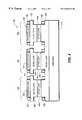
- FIG. 8illustrates a light emitting device having multiple pixels where each pixel have a mesa-like structure according to the embodiment of the present invention.
- Light-emitting device 800includes substrate 810 , device layer 820 , and pixels 830 , 840 and 850 .
- Pixel 830includes contact 831 , phosphor layer 832 , device layer 833 , active layer 834 and contact 835 .
- pixel 840includes contact 841 , phosphor layer 842 , device layer 843 , active layer 844 and contact 845 .
- pixel 850includes contact 851 , phosphor layer 852 , device layer 853 , active layer 854 , and contact 855 .
- a given pixel or multiple pixels of light-emitting device 800 showed in FIG. 8can have a mesa structure.
- the following discussionrelate to pixel 830 , although an analogous structure can also be implemented for pixels 840 and 850 , as well as any other pixels (not shown) of a two-dimensional pixel array for light-emitting device 800 .
- Device layer 833which is disposed between and in contact with phosphor layer 832 and active layer 834 , has a first side that is adjacent to active layer 834 and a second side that is adjacent to phosphor layer 832 and a sidewall 836 .
- a medium exterior to sidewall 836is labeled in FIG. 8 as 860 and has its own refractive index.
- Sidewall 836can be inclined at angle, ⁇ .
- This incline angle, ⁇should be less than 90 degrees and as discussed above can vary between 40 and 60 degrees according to the above-described relationship between ⁇ , the refractive index of exterior medium and the refractive index of the device layer 833 .
- the analogous sidewalls of active layer 834 and the portion of device layer 820 adjacent to active layer 834can also be inclined at an angle, such as, for example, the incline angle, ⁇ .
Landscapes
- Led Device Packages (AREA)
- Led Devices (AREA)
Abstract
Description
| Wave- | |||
| length | |||
| of max. | Photon conversion efficiency | ||
| emission | at wavelength of excitation: | ||
| Coating: | (nm) | 254 nm | 312 nm | 365 nm | 405 nm | 436 nm |
| PPO in 2045 | 400 | 0.49 | 0.80 | — | — | — |
| Bis-MSB in | 450 | 0.74 | 0.93 | 0.94 | — | — |
| 2045 | ||||||
| “Blue Coat- | 430 | 0.93 | 0.92 | 0.95 | — | — |
| ing”(p- | ||||||
| terph. + | ||||||
| PPO + | ||||||
| Bis-MSB in | ||||||
| 2045) | ||||||
| Hostasol 8G | 510 | 0.12 | 0.21 | 0.10 | 0.18 | 0.17 |
| Laser dye | 490 | 0.75 | 0.39 | 0.83 | 0.91 | 0.90 |
| #481 in 2045 | ||||||
| 520 | 0.21 | 0.10 | 0.28 | 0.34 | 0.36 | |
| #495 in 2045 | ||||||
| “Green Coat- | 510 | 0.80 | 0.42 | 0.85 | 0.95 | 0.95 |
| ing” (#481 + | ||||||
| Hostasol 8G | ||||||
| in 2045) | ||||||
| BBQ in 2045 | 495 | 0.78 | 0.62 | 0.83 | 0.87 | 0.82 |
| “Red Coat- | 610 | 0.55 | 0.38 | 0.76 | 0.90 | 0.93 |
| ing” (#481 + | ||||||
| Hostasol 8G | ||||||
| & Hostasol | ||||||
| GG in 2045) | ||||||


Claims (27)
Priority Applications (10)
| Application Number | Priority Date | Filing Date | Title |
|---|---|---|---|
| US09/420,905US6366018B1 (en) | 1998-10-21 | 1999-10-20 | Apparatus for performing wavelength-conversion using phosphors with light emitting diodes |
| EP99970780AEP1141990A4 (en) | 1998-10-21 | 1999-10-21 | WAVE LENGTH CONVERSION DEVICE USING A FLUORATE WITH LIGHT-EMITTING DIODES |
| IL14250999AIL142509A0 (en) | 1998-10-21 | 1999-10-21 | Apparatus for performing wavelength-conversion using phosphors with light emitting diodes |
| CA002347627ACA2347627C (en) | 1998-10-21 | 1999-10-21 | Apparatus for performing wavelength-conversion using phosphors with light emitting diodes |
| KR1020017004819AKR100629042B1 (en) | 1998-10-21 | 1999-10-21 | Apparatus having light-emitting diode and performing wavelength-conversion using phosphor |
| JP2000577686AJP2002528890A (en) | 1998-10-21 | 1999-10-21 | Wavelength conversion performing device using phosphor having light emitting diode |
| PCT/US1999/024902WO2000024024A1 (en) | 1998-10-21 | 1999-10-21 | Apparatus for performing wavelength-conversion using phosphors with light emitting diodes |
| CN99812484ACN1324494A (en) | 1998-10-21 | 1999-10-21 | Apparatus for wavelength conversion of light-emitting diodes using fluorescent substances |
| AU14510/00AAU1451000A (en) | 1998-10-21 | 1999-10-21 | Apparatus for performing wavelength-conversion using phosphors with light emitting diodes |
| JP2010120760AJP2010187028A (en) | 1998-10-21 | 2010-05-26 | Apparatus for performing wavelength-conversion using phosphor with light emitting diode |
Applications Claiming Priority (2)
| Application Number | Priority Date | Filing Date | Title |
|---|---|---|---|
| US10505698P | 1998-10-21 | 1998-10-21 | |
| US09/420,905US6366018B1 (en) | 1998-10-21 | 1999-10-20 | Apparatus for performing wavelength-conversion using phosphors with light emitting diodes |
Publications (1)
| Publication Number | Publication Date |
|---|---|
| US6366018B1true US6366018B1 (en) | 2002-04-02 |
Family
ID=26802207
Family Applications (1)
| Application Number | Title | Priority Date | Filing Date |
|---|---|---|---|
| US09/420,905Expired - LifetimeUS6366018B1 (en) | 1998-10-21 | 1999-10-20 | Apparatus for performing wavelength-conversion using phosphors with light emitting diodes |
Country Status (9)
| Country | Link |
|---|---|
| US (1) | US6366018B1 (en) |
| EP (1) | EP1141990A4 (en) |
| JP (2) | JP2002528890A (en) |
| KR (1) | KR100629042B1 (en) |
| CN (1) | CN1324494A (en) |
| AU (1) | AU1451000A (en) |
| CA (1) | CA2347627C (en) |
| IL (1) | IL142509A0 (en) |
| WO (1) | WO2000024024A1 (en) |
Cited By (47)
| Publication number | Priority date | Publication date | Assignee | Title |
|---|---|---|---|---|
| US20040116033A1 (en)* | 2003-01-27 | 2004-06-17 | 3M Innovative Properties Company | Methods of making phosphor based light sources having an interference reflector |
| US20040145895A1 (en)* | 2003-01-27 | 2004-07-29 | 3M Innovative Properties Company | Phosphor based light sources having a non-planar long pass reflector and method of making |
| US20040145913A1 (en)* | 2003-01-27 | 2004-07-29 | 3M Innovative Properties Company | Phosphor based light sources having a polymeric long pass reflector |
| US20040145289A1 (en)* | 2003-01-27 | 2004-07-29 | 3M Innovative Properties Company | Phosphor based light sources having a non-planar short pass reflector and method of making |
| US20040145312A1 (en)* | 2003-01-27 | 2004-07-29 | 3M Innovative Properties Company | Phosphor based light source having a flexible short pass reflector |
| US20040150997A1 (en)* | 2003-01-27 | 2004-08-05 | 3M Innovative Properties Company | Phosphor based light sources having a reflective polarizer |
| US20040159900A1 (en)* | 2003-01-27 | 2004-08-19 | 3M Innovative Properties Company | Phosphor based light sources having front illumination |
| US20040206936A1 (en)* | 2003-04-21 | 2004-10-21 | Sarnoff Corporation | High efficiency alkaline earth metal thiogallate-based phosphors |
| US20040206973A1 (en)* | 2003-04-21 | 2004-10-21 | Sarnoff Corporation | Methods and devices using high efficiency alkaline earth metal thiogallate-based phosphors |
| KR100499129B1 (en)* | 2002-09-02 | 2005-07-04 | 삼성전기주식회사 | Light emitting laser diode and fabricatin method thereof |
| WO2005120135A1 (en)* | 2004-06-04 | 2005-12-15 | Philips Intellectual Property & Standards Gmbh | Electroluminescent structure and led with an el structure |
| US20060012287A1 (en)* | 2004-07-06 | 2006-01-19 | Sarnoff Corporation | Efficient, green-emitting phosphors, and combinations with red-emitting phosphors |
| US20060038195A1 (en)* | 2002-12-13 | 2006-02-23 | Shyi-Ming Pan | Light-emitting diode and the manufacturing method of the same |
| US20060061259A1 (en)* | 2004-09-23 | 2006-03-23 | Negley Gerald H | Semiconductor light emitting devices including patternable films comprising transparent silicone and phosphor, and methods of manufacturing same |
| US7091653B2 (en) | 2003-01-27 | 2006-08-15 | 3M Innovative Properties Company | Phosphor based light sources having a non-planar long pass reflector |
| US20060214175A1 (en)* | 2005-03-25 | 2006-09-28 | Sarnoff Corporation | Metal silicate-silica-based polymorphous phosphors and lighting devices |
| US20070114559A1 (en)* | 2005-11-23 | 2007-05-24 | Visteon Global Technologies, Inc. | Light emitting diode device having a shield and/or filter |
| US20070125982A1 (en)* | 2005-12-02 | 2007-06-07 | Sarnoff Corporation | Metal silicate halide phosphors and LED lighting devices using the same |
| US20070125984A1 (en)* | 2005-12-01 | 2007-06-07 | Sarnoff Corporation | Phosphors protected against moisture and LED lighting devices |
| US20070182299A1 (en)* | 2003-01-27 | 2007-08-09 | 3M Innovative Properties Company | Phosphor based light source component |
| US20080128679A1 (en)* | 2006-10-03 | 2008-06-05 | Yongchi Tian | Metal silicate halide phosphors and led lighting devices using the same |
| US20080173884A1 (en)* | 2007-01-22 | 2008-07-24 | Cree, Inc. | Wafer level phosphor coating method and devices fabricated utilizing method |
| US20080179611A1 (en)* | 2007-01-22 | 2008-07-31 | Cree, Inc. | Wafer level phosphor coating method and devices fabricated utilizing method |
| US20080185972A1 (en)* | 2006-12-22 | 2008-08-07 | Oki Data Corporation | Light emitting display device |
| US20090040745A1 (en)* | 2007-05-08 | 2009-02-12 | Luminus Devices, Inc. | Light emitting devices including wavelength converting material |
| US20090057690A1 (en)* | 2007-01-22 | 2009-03-05 | Cree, Inc. | Wafer level phosphor coating technique for warm light emitting diodes |
| US20090153022A1 (en)* | 2007-12-14 | 2009-06-18 | Hussell Christopher P | Phosphor distribution in LED lamps using centrifugal force |
| US20090278156A1 (en)* | 2003-09-18 | 2009-11-12 | Leung Michael S | Molded chip fabrication method and apparatus |
| US20090309114A1 (en)* | 2008-01-16 | 2009-12-17 | Luminus Devices, Inc. | Wavelength converting light-emitting devices and methods of making the same |
| US7675079B1 (en)* | 2004-10-28 | 2010-03-09 | Kley Victor B | Diamond coating of silicon-carbide LEDs |
| US20100123145A1 (en)* | 2008-11-18 | 2010-05-20 | Sang Youl Lee | Light emitting device and light emitting device package having the same |
| US20100320480A1 (en)* | 2009-06-19 | 2010-12-23 | Honeywell International Inc. | Phosphor converting ir leds |
| US20110140129A1 (en)* | 2008-09-04 | 2011-06-16 | Leatherdale Catherine A | Light source with improved monochromaticity |
| US20110140128A1 (en)* | 2008-09-04 | 2011-06-16 | Leatherdale Catherine A | Monochromatic light source with high aspect ratio |
| US20110150020A1 (en)* | 2008-09-04 | 2011-06-23 | 3M Innovative Properties Company | Ii-vi mqw vscel on a heat sink optically pumped by a gan ld |
| US20110150019A1 (en)* | 2008-09-04 | 2011-06-23 | Leatherdale Catherine A | Monochromatic light source |
| WO2013017339A1 (en)* | 2011-08-01 | 2013-02-07 | Osram Ag | Wavelength conversion body and method for manufacturing same |
| US8878219B2 (en) | 2008-01-11 | 2014-11-04 | Cree, Inc. | Flip-chip phosphor coating method and devices fabricated utilizing method |
| US9041285B2 (en) | 2007-12-14 | 2015-05-26 | Cree, Inc. | Phosphor distribution in LED lamps using centrifugal force |
| US9166126B2 (en) | 2011-01-31 | 2015-10-20 | Cree, Inc. | Conformally coated light emitting devices and methods for providing the same |
| JP2016076578A (en)* | 2014-10-06 | 2016-05-12 | 日本放送協会 | Light emission element |
| US9634200B2 (en) | 2015-01-20 | 2017-04-25 | Stanley Electric Co., Ltd. | Semiconductor light emitting device |
| US10546846B2 (en) | 2010-07-23 | 2020-01-28 | Cree, Inc. | Light transmission control for masking appearance of solid state light sources |
| US11018283B2 (en) | 2016-10-25 | 2021-05-25 | Osram Oled Gmbh | Method of producing optoelectronic semiconductor components and an optoelectronic semiconductor component |
| US11239394B2 (en)* | 2016-03-18 | 2022-02-01 | Lg Innotek Co., Ltd. | Semiconductor device and display device including the same |
| US11796857B2 (en) | 2016-09-12 | 2023-10-24 | Seoul Semiconductor Co., Ltd. | Display apparatus |
| US12199213B2 (en) | 2018-03-02 | 2025-01-14 | Sharp Kabushiki Kaisha | Image display device |
Families Citing this family (18)
| Publication number | Priority date | Publication date | Assignee | Title |
|---|---|---|---|---|
| JP4928046B2 (en) | 2000-06-29 | 2012-05-09 | コーニンクレッカ フィリップス エレクトロニクス エヌ ヴィ | Photoelectric element |
| US6642652B2 (en) | 2001-06-11 | 2003-11-04 | Lumileds Lighting U.S., Llc | Phosphor-converted light emitting device |
| US6576488B2 (en)* | 2001-06-11 | 2003-06-10 | Lumileds Lighting U.S., Llc | Using electrophoresis to produce a conformally coated phosphor-converted light emitting semiconductor |
| US6660928B1 (en) | 2002-04-02 | 2003-12-09 | Essential Research, Inc. | Multi-junction photovoltaic cell |
| JP2004047748A (en)* | 2002-07-12 | 2004-02-12 | Stanley Electric Co Ltd | Light emitting diode |
| WO2005048364A1 (en)* | 2003-11-12 | 2005-05-26 | Cree, Inc. | Light emitting devices with self aligned ohmic contact and methods of fabricating same |
| US7550579B2 (en) | 2005-04-29 | 2009-06-23 | Pioneer Hi-Bred International, Inc. | Pericarp-preferred regulatory element |
| US7196354B1 (en)* | 2005-09-29 | 2007-03-27 | Luminus Devices, Inc. | Wavelength-converting light-emitting devices |
| KR100849887B1 (en)* | 2007-02-08 | 2008-08-04 | 주식회사 파워라이텍 | White light emitting diode chip using blue chip and phosphor |
| JP5634003B2 (en)* | 2007-09-29 | 2014-12-03 | 日亜化学工業株式会社 | Light emitting device |
| DE102011015726B9 (en)* | 2011-03-31 | 2023-07-13 | OSRAM Opto Semiconductors Gesellschaft mit beschränkter Haftung | Semiconductor chip, display with a plurality of semiconductor chips and method for their production |
| KR101370575B1 (en)* | 2012-07-30 | 2014-03-07 | 주식회사 세미콘라이트 | Semiconductor light emimitting device |
| CN103700749A (en)* | 2012-09-28 | 2014-04-02 | 上海蓝光科技有限公司 | Light-emitting diode and manufacturing method thereof |
| JP2015056652A (en)* | 2013-09-13 | 2015-03-23 | 株式会社東芝 | Nitride semiconductor light emitting device |
| CN105304060B (en)* | 2014-07-22 | 2018-08-10 | 联想(北京)有限公司 | A kind of light detection method and wearable electronic equipment |
| TWI547750B (en)* | 2014-10-13 | 2016-09-01 | 台達電子工業股份有限公司 | Optical wavelength-converting device and illumination system using same |
| CN104393151A (en)* | 2014-10-30 | 2015-03-04 | 大恒新纪元科技股份有限公司 | LED chip enhancing luminescence efficiency and preparation method thereof |
| JP2018190830A (en)* | 2017-05-08 | 2018-11-29 | 豊田合成株式会社 | Semiconductor light-emitting device |
Citations (18)
| Publication number | Priority date | Publication date | Assignee | Title |
|---|---|---|---|---|
| US5399499A (en) | 1994-05-13 | 1995-03-21 | Eastman Kodak Company | Method of using multiwavelength upconversion for sample element interrogation in medical diagnostic equipment |
| US5684360A (en) | 1995-07-10 | 1997-11-04 | Intevac, Inc. | Electron sources utilizing negative electron affinity photocathodes with ultra-small emission areas |
| US5813753A (en) | 1997-05-27 | 1998-09-29 | Philips Electronics North America Corporation | UV/blue led-phosphor device with efficient conversion of UV/blues light to visible light |
| US5813752A (en)* | 1997-05-27 | 1998-09-29 | Philips Electronics North America Corporation | UV/blue LED-phosphor device with short wave pass, long wave pass band pass and peroit filters |
| US5835119A (en) | 1995-10-31 | 1998-11-10 | Hewlett- Packard Company | Face emitting electroluminescent exposure array |
| US5847507A (en) | 1997-07-14 | 1998-12-08 | Hewlett-Packard Company | Fluorescent dye added to epoxy of light emitting diode lens |
| US5851063A (en) | 1996-10-28 | 1998-12-22 | General Electric Company | Light-emitting diode white light source |
| US5886401A (en) | 1997-09-02 | 1999-03-23 | General Electric Company | Structure and fabrication method for interconnecting light emitting diodes with metallization extending through vias in a polymer film overlying the light emitting diodes |
| US5895932A (en) | 1997-01-24 | 1999-04-20 | International Business Machines Corporation | Hybrid organic-inorganic semiconductor light emitting diodes |
| US5898185A (en) | 1997-01-24 | 1999-04-27 | International Business Machines Corporation | Hybrid organic-inorganic semiconductor light emitting diodes |
| EP0936682A1 (en) | 1996-07-29 | 1999-08-18 | Nichia Chemical Industries, Ltd. | Light emitting device and display device |
| US5952681A (en)* | 1997-11-24 | 1999-09-14 | Chen; Hsing | Light emitting diode emitting red, green and blue light |
| US5959316A (en) | 1998-09-01 | 1999-09-28 | Hewlett-Packard Company | Multiple encapsulation of phosphor-LED devices |
| US5959307A (en) | 1995-11-06 | 1999-09-28 | Nichia Chemical Industries Ltd. | Nitride semiconductor device |
| US5962843A (en) | 1997-07-17 | 1999-10-05 | Sinor; Timothy Wayne | Night vision having an image intensifier tube, improved transmission mode photocathode for such a device, and method of making |
| US5982092A (en) | 1997-10-06 | 1999-11-09 | Chen; Hsing | Light Emitting Diode planar light source with blue light or ultraviolet ray-emitting luminescent crystal with optional UV filter |
| US5994722A (en) | 1996-10-31 | 1999-11-30 | Siemens Aktiengesellschaft | Image display device that emits multicolored light |
| US6121726A (en)* | 1996-12-18 | 2000-09-19 | Tdk Corporation | Organic electroluminescent color display having color transmitting layers and fluorescence converting layer with improved structure for color conversion efficiency on a color transmitting layer |
Family Cites Families (11)
| Publication number | Priority date | Publication date | Assignee | Title |
|---|---|---|---|---|
| US4152711A (en)* | 1976-04-01 | 1979-05-01 | Mitsubishi Denki Kabuchiki Kaisha | Semiconductor controlled luminescent device |
| DE3106798A1 (en)* | 1981-02-24 | 1982-09-09 | Licentia Patent-Verwaltungs-Gmbh, 6000 Frankfurt | Semiconductor arrangement |
| JPH04343484A (en)* | 1991-05-21 | 1992-11-30 | Eastman Kodak Japan Kk | Luminous diode array |
| US5406095A (en)* | 1992-08-27 | 1995-04-11 | Victor Company Of Japan, Ltd. | Light emitting diode array and production method of the light emitting diode |
| JPH06169104A (en)* | 1992-11-27 | 1994-06-14 | Victor Co Of Japan Ltd | Emiconductor light-emitting device and manufacture thereof |
| JP2964822B2 (en)* | 1993-02-19 | 1999-10-18 | 日亜化学工業株式会社 | Manufacturing method of light emitting diode |
| JPH09153644A (en)* | 1995-11-30 | 1997-06-10 | Toyoda Gosei Co Ltd | Group-iii nitride semiconductor display device |
| JP3409958B2 (en)* | 1995-12-15 | 2003-05-26 | 株式会社東芝 | Semiconductor light emitting device |
| JP3667414B2 (en)* | 1996-01-16 | 2005-07-06 | ハリソン東芝ライティング株式会社 | Cold cathode low pressure discharge lamp |
| EP0856202A2 (en)* | 1996-06-11 | 1998-08-05 | Koninklijke Philips Electronics N.V. | Visible light emitting devices including uv-light emitting diode and uv-excitable, visible light emitting phosphor, and method of producing such devices |
| EP0977280A3 (en)* | 1998-07-28 | 2008-11-26 | Interuniversitair Micro-Elektronica Centrum Vzw | Devices for emitting radiation with a high efficiency and a method for fabricating such devices |
- 1999
- 1999-10-20USUS09/420,905patent/US6366018B1/ennot_activeExpired - Lifetime
- 1999-10-21CACA002347627Apatent/CA2347627C/ennot_activeExpired - Fee Related
- 1999-10-21WOPCT/US1999/024902patent/WO2000024024A1/enactiveIP Right Grant
- 1999-10-21CNCN99812484Apatent/CN1324494A/enactivePending
- 1999-10-21JPJP2000577686Apatent/JP2002528890A/enactivePending
- 1999-10-21ILIL14250999Apatent/IL142509A0/enunknown
- 1999-10-21EPEP99970780Apatent/EP1141990A4/ennot_activeWithdrawn
- 1999-10-21KRKR1020017004819Apatent/KR100629042B1/ennot_activeExpired - Fee Related
- 1999-10-21AUAU14510/00Apatent/AU1451000A/ennot_activeAbandoned
- 2010
- 2010-05-26JPJP2010120760Apatent/JP2010187028A/enactivePending
Patent Citations (19)
| Publication number | Priority date | Publication date | Assignee | Title |
|---|---|---|---|---|
| US5399499A (en) | 1994-05-13 | 1995-03-21 | Eastman Kodak Company | Method of using multiwavelength upconversion for sample element interrogation in medical diagnostic equipment |
| US5684360A (en) | 1995-07-10 | 1997-11-04 | Intevac, Inc. | Electron sources utilizing negative electron affinity photocathodes with ultra-small emission areas |
| US5835119A (en) | 1995-10-31 | 1998-11-10 | Hewlett- Packard Company | Face emitting electroluminescent exposure array |
| US5959307A (en) | 1995-11-06 | 1999-09-28 | Nichia Chemical Industries Ltd. | Nitride semiconductor device |
| EP0936682A1 (en) | 1996-07-29 | 1999-08-18 | Nichia Chemical Industries, Ltd. | Light emitting device and display device |
| US5998925A (en)* | 1996-07-29 | 1999-12-07 | Nichia Kagaku Kogyo Kabushiki Kaisha | Light emitting device having a nitride compound semiconductor and a phosphor containing a garnet fluorescent material |
| US5851063A (en) | 1996-10-28 | 1998-12-22 | General Electric Company | Light-emitting diode white light source |
| US5994722A (en) | 1996-10-31 | 1999-11-30 | Siemens Aktiengesellschaft | Image display device that emits multicolored light |
| US6121726A (en)* | 1996-12-18 | 2000-09-19 | Tdk Corporation | Organic electroluminescent color display having color transmitting layers and fluorescence converting layer with improved structure for color conversion efficiency on a color transmitting layer |
| US5895932A (en) | 1997-01-24 | 1999-04-20 | International Business Machines Corporation | Hybrid organic-inorganic semiconductor light emitting diodes |
| US5898185A (en) | 1997-01-24 | 1999-04-27 | International Business Machines Corporation | Hybrid organic-inorganic semiconductor light emitting diodes |
| US5813752A (en)* | 1997-05-27 | 1998-09-29 | Philips Electronics North America Corporation | UV/blue LED-phosphor device with short wave pass, long wave pass band pass and peroit filters |
| US5813753A (en) | 1997-05-27 | 1998-09-29 | Philips Electronics North America Corporation | UV/blue led-phosphor device with efficient conversion of UV/blues light to visible light |
| US5847507A (en) | 1997-07-14 | 1998-12-08 | Hewlett-Packard Company | Fluorescent dye added to epoxy of light emitting diode lens |
| US5962843A (en) | 1997-07-17 | 1999-10-05 | Sinor; Timothy Wayne | Night vision having an image intensifier tube, improved transmission mode photocathode for such a device, and method of making |
| US5886401A (en) | 1997-09-02 | 1999-03-23 | General Electric Company | Structure and fabrication method for interconnecting light emitting diodes with metallization extending through vias in a polymer film overlying the light emitting diodes |
| US5982092A (en) | 1997-10-06 | 1999-11-09 | Chen; Hsing | Light Emitting Diode planar light source with blue light or ultraviolet ray-emitting luminescent crystal with optional UV filter |
| US5952681A (en)* | 1997-11-24 | 1999-09-14 | Chen; Hsing | Light emitting diode emitting red, green and blue light |
| US5959316A (en) | 1998-09-01 | 1999-09-28 | Hewlett-Packard Company | Multiple encapsulation of phosphor-LED devices |
Non-Patent Citations (9)
| Title |
|---|
| Applied Physics Letters, American Institute of Physics, vol. 59, No. 12, "Reflective filters based on single-crystal GAN/A1xGA1-xN multilayers deposited using low-pressure metalorganic chemical vapor deposition", Sep. 16, 1991, pp. 1449-1451. |
| Applied Physics Letters, American Institute of Physics, vol. 67, No. 13, "High-power InGAN single-quantum-well-structure blue and violet light-emitting diodes", Sep. 25, 1995, pp. 1868-1870. |
| Denbaars S. P., Gallium-nitride based materials for blue to utaviolet optoelectronics devices, IEEE vol. 5 Nov. 11, 1997. |
| Journal of Applied Physics, American Institute of Physics, vol. 80, No. 8, "Organic films deposited on Si p-n junctions: Accurate measurements on fluorescence internal efficiency, and application ot luminescent antireflection coating", Oct. 15, 1996, pp. 4644-4648. |
| Nakamara, S. "III-V Nitride-Based Short-Wavelength LEDs and LDs"S, Series on Semiconductor Science Technology, Oxford University Press Inc., #6, 1998, pp 391-416. |
| PCT International Search Report corresponding to PCT Application PCT/US99/24902. |
| PCT International Search Report corresponding to PCT Application PCT/US99/24911. |
| Physical Review Letters, The American Physical Society, vol. 72, No. 3, "Optical Properties of Manganese-Doped Nanocrystals of ZnS", Jan. 17, 1994, pp. 416-419. |
| Walter Viehman, SPIE, vol. 196, Measurement of Optical Radiations, "Thin-film scintillators for extended ultraviolet (UV) response silicon detectors", 1979, pp. 90-95. |
Cited By (89)
| Publication number | Priority date | Publication date | Assignee | Title |
|---|---|---|---|---|
| KR100499129B1 (en)* | 2002-09-02 | 2005-07-04 | 삼성전기주식회사 | Light emitting laser diode and fabricatin method thereof |
| US20060038195A1 (en)* | 2002-12-13 | 2006-02-23 | Shyi-Ming Pan | Light-emitting diode and the manufacturing method of the same |
| US7210977B2 (en) | 2003-01-27 | 2007-05-01 | 3M Innovative Properties Comapny | Phosphor based light source component and method of making |
| US7312560B2 (en) | 2003-01-27 | 2007-12-25 | 3M Innovative Properties | Phosphor based light sources having a non-planar long pass reflector and method of making |
| US20040145312A1 (en)* | 2003-01-27 | 2004-07-29 | 3M Innovative Properties Company | Phosphor based light source having a flexible short pass reflector |
| US20040150997A1 (en)* | 2003-01-27 | 2004-08-05 | 3M Innovative Properties Company | Phosphor based light sources having a reflective polarizer |
| US20040159900A1 (en)* | 2003-01-27 | 2004-08-19 | 3M Innovative Properties Company | Phosphor based light sources having front illumination |
| US20070182299A1 (en)* | 2003-01-27 | 2007-08-09 | 3M Innovative Properties Company | Phosphor based light source component |
| US7245072B2 (en) | 2003-01-27 | 2007-07-17 | 3M Innovative Properties Company | Phosphor based light sources having a polymeric long pass reflector |
| US20040145913A1 (en)* | 2003-01-27 | 2004-07-29 | 3M Innovative Properties Company | Phosphor based light sources having a polymeric long pass reflector |
| US7091653B2 (en) | 2003-01-27 | 2006-08-15 | 3M Innovative Properties Company | Phosphor based light sources having a non-planar long pass reflector |
| US20040116033A1 (en)* | 2003-01-27 | 2004-06-17 | 3M Innovative Properties Company | Methods of making phosphor based light sources having an interference reflector |
| US20040145895A1 (en)* | 2003-01-27 | 2004-07-29 | 3M Innovative Properties Company | Phosphor based light sources having a non-planar long pass reflector and method of making |
| US7394188B2 (en) | 2003-01-27 | 2008-07-01 | 3M Innovative Properties Company | Phosphor based light source component |
| US20040145289A1 (en)* | 2003-01-27 | 2004-07-29 | 3M Innovative Properties Company | Phosphor based light sources having a non-planar short pass reflector and method of making |
| US7091661B2 (en) | 2003-01-27 | 2006-08-15 | 3M Innovative Properties Company | Phosphor based light sources having a reflective polarizer |
| US7157839B2 (en) | 2003-01-27 | 2007-01-02 | 3M Innovative Properties Company | Phosphor based light sources utilizing total internal reflection |
| US7118438B2 (en) | 2003-01-27 | 2006-10-10 | 3M Innovative Properties Company | Methods of making phosphor based light sources having an interference reflector |
| US7125501B2 (en) | 2003-04-21 | 2006-10-24 | Sarnoff Corporation | High efficiency alkaline earth metal thiogallate-based phosphors |
| US20040206973A1 (en)* | 2003-04-21 | 2004-10-21 | Sarnoff Corporation | Methods and devices using high efficiency alkaline earth metal thiogallate-based phosphors |
| US20040206936A1 (en)* | 2003-04-21 | 2004-10-21 | Sarnoff Corporation | High efficiency alkaline earth metal thiogallate-based phosphors |
| US7368179B2 (en) | 2003-04-21 | 2008-05-06 | Sarnoff Corporation | Methods and devices using high efficiency alkaline earth metal thiogallate-based phosphors |
| US9105817B2 (en) | 2003-09-18 | 2015-08-11 | Cree, Inc. | Molded chip fabrication method and apparatus |
| US10164158B2 (en) | 2003-09-18 | 2018-12-25 | Cree, Inc. | Molded chip fabrication method and apparatus |
| US9093616B2 (en) | 2003-09-18 | 2015-07-28 | Cree, Inc. | Molded chip fabrication method and apparatus |
| US20110169038A1 (en)* | 2003-09-18 | 2011-07-14 | Cree, Inc. | Molded chip fabrication method and apparatus |
| US10546978B2 (en) | 2003-09-18 | 2020-01-28 | Cree, Inc. | Molded chip fabrication method and apparatus |
| US20090278156A1 (en)* | 2003-09-18 | 2009-11-12 | Leung Michael S | Molded chip fabrication method and apparatus |
| WO2005120135A1 (en)* | 2004-06-04 | 2005-12-15 | Philips Intellectual Property & Standards Gmbh | Electroluminescent structure and led with an el structure |
| US20070252512A1 (en)* | 2004-06-04 | 2007-11-01 | Koninklijke Philips Electronics, N.V. | Electroluminescent Structure and Led with an El Structure |
| US20060012287A1 (en)* | 2004-07-06 | 2006-01-19 | Sarnoff Corporation | Efficient, green-emitting phosphors, and combinations with red-emitting phosphors |
| US7427366B2 (en) | 2004-07-06 | 2008-09-23 | Sarnoff Corporation | Efficient, green-emitting phosphors, and combinations with red-emitting phosphors |
| US20080076316A1 (en)* | 2004-09-23 | 2008-03-27 | Cree, Inc. | Methods of manufacturing semiconductor light emitting devices including patternable films comprising transparent silicone and phosphor |
| US7372198B2 (en) | 2004-09-23 | 2008-05-13 | Cree, Inc. | Semiconductor light emitting devices including patternable films comprising transparent silicone and phosphor |
| WO2006036251A1 (en)* | 2004-09-23 | 2006-04-06 | Cree, Inc. | Semiconductor light emitting devices including patternable films comprising transparent silicone and phosphor, and methods of manufacturing same |
| US20060061259A1 (en)* | 2004-09-23 | 2006-03-23 | Negley Gerald H | Semiconductor light emitting devices including patternable films comprising transparent silicone and phosphor, and methods of manufacturing same |
| US7591702B2 (en) | 2004-09-23 | 2009-09-22 | Cree, Inc. | Methods of manufacturing semiconductor light emitting devices including patternable films comprising phosphor |
| US7675079B1 (en)* | 2004-10-28 | 2010-03-09 | Kley Victor B | Diamond coating of silicon-carbide LEDs |
| US7276183B2 (en) | 2005-03-25 | 2007-10-02 | Sarnoff Corporation | Metal silicate-silica-based polymorphous phosphors and lighting devices |
| US20060214175A1 (en)* | 2005-03-25 | 2006-09-28 | Sarnoff Corporation | Metal silicate-silica-based polymorphous phosphors and lighting devices |
| US20070114559A1 (en)* | 2005-11-23 | 2007-05-24 | Visteon Global Technologies, Inc. | Light emitting diode device having a shield and/or filter |
| US7564070B2 (en) | 2005-11-23 | 2009-07-21 | Visteon Global Technologies, Inc. | Light emitting diode device having a shield and/or filter |
| US20070125984A1 (en)* | 2005-12-01 | 2007-06-07 | Sarnoff Corporation | Phosphors protected against moisture and LED lighting devices |
| US20070125982A1 (en)* | 2005-12-02 | 2007-06-07 | Sarnoff Corporation | Metal silicate halide phosphors and LED lighting devices using the same |
| US8906262B2 (en) | 2005-12-02 | 2014-12-09 | Lightscape Materials, Inc. | Metal silicate halide phosphors and LED lighting devices using the same |
| US20080128679A1 (en)* | 2006-10-03 | 2008-06-05 | Yongchi Tian | Metal silicate halide phosphors and led lighting devices using the same |
| US7713442B2 (en) | 2006-10-03 | 2010-05-11 | Lightscape Materials, Inc. | Metal silicate halide phosphors and LED lighting devices using the same |
| US20080185972A1 (en)* | 2006-12-22 | 2008-08-07 | Oki Data Corporation | Light emitting display device |
| US9159888B2 (en) | 2007-01-22 | 2015-10-13 | Cree, Inc. | Wafer level phosphor coating method and devices fabricated utilizing method |
| US8232564B2 (en) | 2007-01-22 | 2012-07-31 | Cree, Inc. | Wafer level phosphor coating technique for warm light emitting diodes |
| US9024349B2 (en) | 2007-01-22 | 2015-05-05 | Cree, Inc. | Wafer level phosphor coating method and devices fabricated utilizing method |
| US20090057690A1 (en)* | 2007-01-22 | 2009-03-05 | Cree, Inc. | Wafer level phosphor coating technique for warm light emitting diodes |
| US20080173884A1 (en)* | 2007-01-22 | 2008-07-24 | Cree, Inc. | Wafer level phosphor coating method and devices fabricated utilizing method |
| US20080179611A1 (en)* | 2007-01-22 | 2008-07-31 | Cree, Inc. | Wafer level phosphor coating method and devices fabricated utilizing method |
| US7781779B2 (en) | 2007-05-08 | 2010-08-24 | Luminus Devices, Inc. | Light emitting devices including wavelength converting material |
| US20090040745A1 (en)* | 2007-05-08 | 2009-02-12 | Luminus Devices, Inc. | Light emitting devices including wavelength converting material |
| US20110012156A1 (en)* | 2007-05-08 | 2011-01-20 | Luminus Devices, Inc. | Light emitting devices including wavelength converting material |
| US8217402B2 (en) | 2007-05-08 | 2012-07-10 | Luminus Devices, Inc. | Light emitting devices including wavelength converting material |
| US9041285B2 (en) | 2007-12-14 | 2015-05-26 | Cree, Inc. | Phosphor distribution in LED lamps using centrifugal force |
| US8167674B2 (en) | 2007-12-14 | 2012-05-01 | Cree, Inc. | Phosphor distribution in LED lamps using centrifugal force |
| US20090153022A1 (en)* | 2007-12-14 | 2009-06-18 | Hussell Christopher P | Phosphor distribution in LED lamps using centrifugal force |
| US8878219B2 (en) | 2008-01-11 | 2014-11-04 | Cree, Inc. | Flip-chip phosphor coating method and devices fabricated utilizing method |
| US9972753B2 (en) | 2008-01-16 | 2018-05-15 | Luminus Devices, Inc. | Wavelength converting light-emitting devices and methods of making the same |
| US20090309114A1 (en)* | 2008-01-16 | 2009-12-17 | Luminus Devices, Inc. | Wavelength converting light-emitting devices and methods of making the same |
| US8488641B2 (en) | 2008-09-04 | 2013-07-16 | 3M Innovative Properties Company | II-VI MQW VSEL on a heat sink optically pumped by a GaN LD |
| US8385380B2 (en) | 2008-09-04 | 2013-02-26 | 3M Innovative Properties Company | Monochromatic light source |
| US8193543B2 (en) | 2008-09-04 | 2012-06-05 | 3M Innovative Properties Company | Monochromatic light source with high aspect ratio |
| US20110150019A1 (en)* | 2008-09-04 | 2011-06-23 | Leatherdale Catherine A | Monochromatic light source |
| US20110150020A1 (en)* | 2008-09-04 | 2011-06-23 | 3M Innovative Properties Company | Ii-vi mqw vscel on a heat sink optically pumped by a gan ld |
| US20110140128A1 (en)* | 2008-09-04 | 2011-06-16 | Leatherdale Catherine A | Monochromatic light source with high aspect ratio |
| US20110140129A1 (en)* | 2008-09-04 | 2011-06-16 | Leatherdale Catherine A | Light source with improved monochromaticity |
| US20100123145A1 (en)* | 2008-11-18 | 2010-05-20 | Sang Youl Lee | Light emitting device and light emitting device package having the same |
| CN101740600B (en)* | 2008-11-18 | 2013-09-04 | Lg伊诺特有限公司 | Light emitting device and led package having the same |
| US8884505B2 (en)* | 2008-11-18 | 2014-11-11 | Lg Innotek Co., Ltd. | Light emitting device including a plurality of light emitting cells and light emitting device package having the same |
| EP2187442A3 (en)* | 2008-11-18 | 2010-12-29 | LG Innotek Co., Ltd. | Light emitting device and light emitting device package having the same |
| US8426871B2 (en) | 2009-06-19 | 2013-04-23 | Honeywell International Inc. | Phosphor converting IR LEDs |
| US20100320480A1 (en)* | 2009-06-19 | 2010-12-23 | Honeywell International Inc. | Phosphor converting ir leds |
| US10546846B2 (en) | 2010-07-23 | 2020-01-28 | Cree, Inc. | Light transmission control for masking appearance of solid state light sources |
| US9166126B2 (en) | 2011-01-31 | 2015-10-20 | Cree, Inc. | Conformally coated light emitting devices and methods for providing the same |
| WO2013017339A1 (en)* | 2011-08-01 | 2013-02-07 | Osram Ag | Wavelength conversion body and method for manufacturing same |
| JP2016076578A (en)* | 2014-10-06 | 2016-05-12 | 日本放送協会 | Light emission element |
| US9634200B2 (en) | 2015-01-20 | 2017-04-25 | Stanley Electric Co., Ltd. | Semiconductor light emitting device |
| US11239394B2 (en)* | 2016-03-18 | 2022-02-01 | Lg Innotek Co., Ltd. | Semiconductor device and display device including the same |
| US11796857B2 (en) | 2016-09-12 | 2023-10-24 | Seoul Semiconductor Co., Ltd. | Display apparatus |
| US12066713B2 (en) | 2016-09-12 | 2024-08-20 | Seoul Semiconductor Co., Ltd. | Display apparatus |
| US11018283B2 (en) | 2016-10-25 | 2021-05-25 | Osram Oled Gmbh | Method of producing optoelectronic semiconductor components and an optoelectronic semiconductor component |
| US11557700B2 (en) | 2016-10-25 | 2023-01-17 | Osram Oled Gmbh | Method of producing optoelectronic semiconductor components and an optoelectronic semiconductor component |
| US12349523B2 (en) | 2016-10-25 | 2025-07-01 | Osram Oled Gmbh | Method of producing optoelectronic semiconductor components and an optoelectronic semiconductor component |
| US12199213B2 (en) | 2018-03-02 | 2025-01-14 | Sharp Kabushiki Kaisha | Image display device |
Also Published As
| Publication number | Publication date |
|---|---|
| CN1324494A (en) | 2001-11-28 |
| CA2347627A1 (en) | 2000-04-27 |
| JP2010187028A (en) | 2010-08-26 |
| IL142509A0 (en) | 2002-03-10 |
| KR20010080203A (en) | 2001-08-22 |
| AU1451000A (en) | 2000-05-08 |
| EP1141990A4 (en) | 2005-02-09 |
| KR100629042B1 (en) | 2006-09-26 |
| JP2002528890A (en) | 2002-09-03 |
| EP1141990A1 (en) | 2001-10-10 |
| CA2347627C (en) | 2010-03-02 |
| WO2000024024A1 (en) | 2000-04-27 |
Similar Documents
| Publication | Publication Date | Title |
|---|---|---|
| US6366018B1 (en) | Apparatus for performing wavelength-conversion using phosphors with light emitting diodes | |
| US6404125B1 (en) | Method and apparatus for performing wavelength-conversion using phosphors with light emitting diodes | |
| US7776629B2 (en) | High efficiency light emitting diode (LED) with optimized photonic crystal extractor | |
| KR102667726B1 (en) | Back light unit | |
| CN100474643C (en) | Semiconductor light emitting device and manufacturing method for semiconductor light emitting device | |
| JP5681002B2 (en) | Light emitting device and projector | |
| US12224375B2 (en) | Light emitting diode with improved colour purity | |
| US20050173714A1 (en) | Lighting system with high and improved extraction efficiency | |
| US6160273A (en) | Diode pumped solid state edge emitting light source | |
| CA2356530A1 (en) | Efficient solid-state light emitting device with excited phosphors for producing a visible light output | |
| KR20100097214A (en) | Radiation-emitting device | |
| KR20190090332A (en) | Back light unit | |
| CN220914235U (en) | A micro display chip structure | |
| KR20110137814A (en) | Light emitting diode | |
| EP0772248B1 (en) | Microactivity LED with photon recycling | |
| KR100946033B1 (en) | Multicolor Light Emitting Device Using Micro Cavity | |
| JP4182848B2 (en) | Planar light emitting device | |
| WO2025025072A1 (en) | Micro led and micro led display panel | |
| CN119008816B (en) | Micro display device and preparation method thereof | |
| TW202508095A (en) | Micro led and micro led display panel | |
| TW202508094A (en) | Micro led and micro led display panel | |
| JP5936017B2 (en) | Light emitting device and projector | |
| TW202508043A (en) | Micro led and micro led display panel | |
| CN120049272A (en) | Diode light emitting device, laser light emitting device, and resonant cavity light emitting device | |
| CN116490987A (en) | High Color Purity Light Emitting Diodes |
Legal Events
| Date | Code | Title | Description |
|---|---|---|---|
| AS | Assignment | Owner name:SARNOFF CORPORATION, NEW JERSEY Free format text:ASSIGNMENT OF ASSIGNORS INTEREST;ASSIGNORS:GARBUZOV, DMITRI ZALMANOVICH;CONNOLLY, JOHN CHARLES;KARLICEK, ROBERT FRANK, JR.;AND OTHERS;REEL/FRAME:010625/0081;SIGNING DATES FROM 20000302 TO 20000306 Owner name:EMCORE CORPORATION, NEW JERSEY Free format text:ASSIGNMENT OF ASSIGNORS INTEREST;ASSIGNORS:GARBUZOV, DMITRI ZALMANOVICH;CONNOLLY, JOHN CHARLES;KARLICEK, ROBERT FRANK, JR.;AND OTHERS;REEL/FRAME:010625/0081;SIGNING DATES FROM 20000302 TO 20000306 | |
| STCF | Information on status: patent grant | Free format text:PATENTED CASE | |
| FPAY | Fee payment | Year of fee payment:4 | |
| AS | Assignment | Owner name:BANK OF AMERICA, N.A., ILLINOIS Free format text:SECURITY AGREEMENT;ASSIGNOR:EMCORE CORPORATION;REEL/FRAME:021824/0019 Effective date:20080926 Owner name:BANK OF AMERICA, N.A.,ILLINOIS Free format text:SECURITY AGREEMENT;ASSIGNOR:EMCORE CORPORATION;REEL/FRAME:021824/0019 Effective date:20080926 | |
| AS | Assignment | Owner name:LIGHTSCAPE MATERIALS, INC., NEW JERSEY Free format text:ASSIGNMENT OF ASSIGNORS INTEREST;ASSIGNOR:SARNOFF CORPORATION;REEL/FRAME:022878/0309 Effective date:20090610 Owner name:LIGHTSCAPE MATERIALS, INC.,NEW JERSEY Free format text:ASSIGNMENT OF ASSIGNORS INTEREST;ASSIGNOR:SARNOFF CORPORATION;REEL/FRAME:022878/0309 Effective date:20090610 | |
| FPAY | Fee payment | Year of fee payment:8 | |
| AS | Assignment | Owner name:THE DOW CHEMICAL COMPANY, AS COLLATERAL AGENT, MIC Free format text:INTELLECTUAL PROPERTY SECURITY AGREEMENT;ASSIGNOR:LIGHTSCAPE MATERIALS, INC.;REEL/FRAME:026170/0042 Effective date:20110422 | |
| AS | Assignment | Owner name:WELLS FARGO BANK, NATIONAL ASSOCIATION, ARIZONA Free format text:SECURITY AGREEMENT;ASSIGNORS:EMCORE CORPORATION;EMCORE SOLAR POWER, INC.;REEL/FRAME:026304/0142 Effective date:20101111 | |
| AS | Assignment | Owner name:EMCORE CORPORATION, NEW MEXICO Free format text:RELEASE BY SECURED PARTY;ASSIGNOR:BANK OF AMERICA, N.A.;REEL/FRAME:027050/0880 Effective date:20110831 Owner name:EMCORE SOLAR POWER, INC., NEW MEXICO Free format text:RELEASE BY SECURED PARTY;ASSIGNOR:BANK OF AMERICA, N.A.;REEL/FRAME:027050/0880 Effective date:20110831 | |
| AS | Assignment | Owner name:ADVANCED TECHNOLOGY MATERIALS, INC., CONNECTICUT Free format text:SECURITY AGREEMENT;ASSIGNOR:LIGHTSCAPE MATERIALS, INC.;REEL/FRAME:027334/0024 Effective date:20111206 | |
| AS | Assignment | Owner name:LIGHTSCAPE MATERIALS, INC., NEW JERSEY Free format text:RELEASE BY SECURED PARTY;ASSIGNOR:THE DOW CHEMICAL COMPANY;REEL/FRAME:027363/0650 Effective date:20111201 | |
| AS | Assignment | Owner name:LIGHTSCAPE MATERIALS, INC., NEW JERSEY Free format text:RELEASE BY SECURED PARTY;ASSIGNOR:ADVANCED TECHNOLOGY MATERIALS, INC.;REEL/FRAME:028202/0239 Effective date:20120514 | |
| FPAY | Fee payment | Year of fee payment:12 |