US6365449B1 - Process for making a non-volatile memory cell with a polysilicon spacer defined select gate - Google Patents
Process for making a non-volatile memory cell with a polysilicon spacer defined select gateDownload PDFInfo
- Publication number
- US6365449B1 US6365449B1US09/657,882US65788200AUS6365449B1US 6365449 B1US6365449 B1US 6365449B1US 65788200 AUS65788200 AUS 65788200AUS 6365449 B1US6365449 B1US 6365449B1
- Authority
- US
- United States
- Prior art keywords
- floating gate
- layer
- region
- polysilicon
- body region
- Prior art date
- Legal status (The legal status is an assumption and is not a legal conclusion. Google has not performed a legal analysis and makes no representation as to the accuracy of the status listed.)
- Expired - Lifetime
Links
- 229910021420polycrystalline siliconInorganic materials0.000titleclaimsabstractdescription92
- 229920005591polysiliconPolymers0.000titleclaimsabstractdescription92
- 238000000034methodMethods0.000titleclaimsabstractdescription30
- 230000015654memoryEffects0.000titleclaimsabstractdescription16
- 125000006850spacer groupChemical group0.000titleclaimsdescription22
- 210000000746body regionAnatomy0.000claimsabstractdescription32
- 230000000873masking effectEffects0.000claimsabstractdescription25
- XUIMIQQOPSSXEZ-UHFFFAOYSA-NSiliconChemical compound[Si]XUIMIQQOPSSXEZ-UHFFFAOYSA-N0.000claimsabstractdescription9
- 229910052710siliconInorganic materials0.000claimsabstractdescription9
- 239000010703siliconSubstances0.000claimsabstractdescription9
- 229920002120photoresistant polymerPolymers0.000claimsdescription8
- 239000004065semiconductorSubstances0.000claimsdescription6
- 239000000758substrateSubstances0.000claimsdescription6
- 239000002131composite materialSubstances0.000claimsdescription3
- 230000008901benefitEffects0.000abstractdescription4
- 238000005530etchingMethods0.000description5
- 238000004519manufacturing processMethods0.000description4
- 238000012545processingMethods0.000description4
- 239000012535impuritySubstances0.000description3
- 230000001419dependent effectEffects0.000description2
- 238000005516engineering processMethods0.000description2
- 239000007943implantSubstances0.000description2
- 238000013459approachMethods0.000description1
- 238000007796conventional methodMethods0.000description1
- 238000009792diffusion processMethods0.000description1
- 238000001459lithographyMethods0.000description1
- 238000012986modificationMethods0.000description1
- 230000004048modificationEffects0.000description1
Images

Classifications
- H—ELECTRICITY
- H10—SEMICONDUCTOR DEVICES; ELECTRIC SOLID-STATE DEVICES NOT OTHERWISE PROVIDED FOR
- H10D—INORGANIC ELECTRIC SEMICONDUCTOR DEVICES
- H10D30/00—Field-effect transistors [FET]
- H10D30/01—Manufacture or treatment
- H10D30/021—Manufacture or treatment of FETs having insulated gates [IGFET]
- H10D30/0411—Manufacture or treatment of FETs having insulated gates [IGFET] of FETs having floating gates
- H—ELECTRICITY
- H10—SEMICONDUCTOR DEVICES; ELECTRIC SOLID-STATE DEVICES NOT OTHERWISE PROVIDED FOR
- H10D—INORGANIC ELECTRIC SEMICONDUCTOR DEVICES
- H10D64/00—Electrodes of devices having potential barriers
- H10D64/01—Manufacture or treatment
- H10D64/031—Manufacture or treatment of data-storage electrodes
- H10D64/035—Manufacture or treatment of data-storage electrodes comprising conductor-insulator-conductor-insulator-semiconductor structures
Definitions
- This inventionrelates to semiconductor memories, and more particularly to a method of manufacturing and a structure of a split-gate non-volatile memory cell which provides a simple and highly accurate means of controlling the cell channel length which is a critical parameter for proper cell operation.
- a conventional method of defining a select gate transistor in a non-volatile memory cellis to use a second layer polysilicon masking step along with a second layer polysilicon etching step.
- the masking and etching stepsdefine a predetermined second layer polysilicon length and a corresponding portion of the cell channel length.
- the channel length of a split-gate cellis typically made-up of a portion under the floating gate plus another portion under the second polysilicon spacer side-wall.
- a deposited second layer polysilicon film with a thickness of 2,500 ⁇creates a spacer width of about 0.25 ⁇ m. If the total channel length target is 0.35 ⁇ m and the floating gate portion of the channel is 0.25 ⁇ m, it leaves the second layer polysilicon lithography step a misalignment tolerance relative to floating gate edges of a mere 0.05 ⁇ m.
- the second polysilicon spacer widthis 0.25 ⁇ m
- the target length for the portion of the channel length defined by the second polysilicon spaceris 0.2 ⁇ m
- a very long over-etchis required to remove the twice-greater thickness of the second polysilicon film along the spacer region (the twice-greater thickness is caused by the step in second polysilicon due to the presence of the floating gate).
- This over-etch stepwhich is also carried out in the periphery CMOS region of the memory device wherein the twice-greater thickness of second polysilicon is not present, can severely pit the silicon in the source and drain junction regions of the periphery transistors. The silicon pitting causes an undesirable leakage current from the source and drain regions to the substrate.
- a method of forming a memory cellincludes: forming a floating gate over a first portion of a silicon body region, the floating gate being insulated from the underlying first portion of the body region; forming a second layer polysilicon over the floating gate and a second portion of the body region, the second layer polysilicon being insulated from the underlying floating gate and the second portion of the body region; and forming a masking layer over the second layer polysilicon, the masking layer having a width along a first dimension parallel to the surface of the body region such that the masking layer extends over an entire width of the floating gate along the first dimension but does not extend beyond edges of steps of the second layer polysilicon formed due to the presence of the floating gate.
- the methodfurther includes performing an etch cycle so that the portions of the second layer polysilicon not covered by the masking layer are etched back by an amount substantially equal to a predefined thickness of the second layer polysilicon.
- the second layer polysilicon in the array regionalso forms polysilicon gates of transistors in the periphery region, the etch cycle being designed to achieve a target critical dimension (CD) for a polysilicon gate length of the periphery transistors.
- CDtarget critical dimension
- the methodfurther includes forming a source region and a drain region in the body region so that an inner edge of each of the source and drain regions is self-aligned to a corresponding outer edge of two second layer polysilicon spacers formed adjacent floating gate side-walls as a result of the etch cycle.
- a portion of the body region bounded by the source and drain regionsforms a channel region having a channel length, a width of each of the second layer polysilicon spacers along the first dimension defining a corresponding portion of the channel length.
- the portions of the channel length corresponding to the spacersare symmetrical about the floating gate.
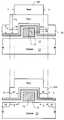
- FIGS. 1A and 1Bshow cross sections of a split-gate non-volatile memory cell at different processing stages in accordance with an embodiment of the present invention.
- a method of manufacturing and a structure of a split-gate non-volatile memory cellprovide a simple and highly accurate means of controlling the select-gate channel portion (and as a result the entire channel length) of the split-gate cell and the periphery polysilicon gate length, without requiring additional masking steps or over-etching of the second layer polysilicon film.
- FIGS. 1A and 1Bshow cross sections of a split-gate non-volatile memory cell at different processing stages.
- the active area of the cellis defined and a tunnel oxide layer 12 having a thickness in the range of 70-100 ⁇ , preferably about 85 ⁇ , is grown over a substrate 22 , as shown in FIG. 1 A.
- a first polysilicon layeris deposited and etched back using a masking layer to define a floating gate layer 14 having a thickness in the range of 1,000 ⁇ to 3,000 ⁇ , preferably about 1,500 ⁇ .
- Floating gate layer 14may be doped with one or more impurities to obtain the desired polysilicon characteristics.
- An insulating composite layer 16 of oxide-nitride-oxide (ONO)is formed over floating gate 14 and other regions of the substrate, as shown in FIG. 1A.
- Second layer polysilicon 18may be doped with one or more impurities to obtain the desired polysilicon characteristics.
- Photoresist masking layer 20is formed over second layer polysilicon 18 as shown.
- Photoresist masking layer 20is defined so that its outer right edge X and outer left edge Y are within the width W 1 of the second polysilicon side walls as shown in FIG. 1 A.
- Width W 1is equal to the thickness t 1 of second polysilicon 18 .
- a second layer polysilicon etch stepis carried out.
- This etch stepis optimized to achieve the desired critical dimensions (CDs) for the polysilicon gate length in the CMOS periphery area and not the array region. This is because in submicron technologies it is highly critical to accurately define the polysilicon gates of CMOS transistors in the periphery region.
- this etch stepresults in removal of the portions of the second layer polysilicon 18 not covered by photoresist 20 , such that polysilicon layer 18 A remains as shown in FIG. 1 B.
- the second layer polysilicon 18 Aforms a polysilicon spacer on the side-walls of floating gate 14 .
- the polysilicon spacer portionsare shown as steps in FIG. 1B for simplicity, although in practice the spacers have smoother edges.
- the spacersare formed as a result of the requirement that the edges X, Y of photoresist 20 be within the width W 1 .
- This techniquetakes advantage of the physical feature of the cell where second polysilicon 18 has a thickness t 2 along the side-walls of floating gate 14 which is about equal to the target thickness t 1 of the second polysilicon plus the thickness t 3 of floating gate 14 .
- This techniquemakes the alignment of second polysilicon masking layer 20 relative to floating gate 14 substantially more relaxed than in the prior art cells because the same second polysilicon side-wall width W 1 (FIG. 1B) is formed regardless of the alignment as long as sides X and Y of masking layer 20 are within the W 1 tolerance.
- source and drain regions 24 and 26are formed in accordance with conventional processing steps.
- an implant stepwhereby n-type impurities are implanted into the source/drain regions may be carried out.
- the outer edges of the second polysilicon spacersmarked as A and B in FIG. 1B, define the inner edges of source and drain regions 24 and 26 .
- the inner edges of the source and drain regionsin turn define the total channel length (i.e., the substrate surface region between source/drain diffusions 24 , 26 ).
- the source and drain regions 24 , 26are self-aligned with the second layer polysilicon, yielding a more scalable memory cell.
- the portions of the channel length marked as Dare defined by the second polysilicon spacer width, which in turn is controlled by the thickness of the deposited second layer polysilicon 18 . If portions D of the channel length are desired to be longer, a thicker second layer polysilicon may be chosen, and vice versa, if portions D are desired to be shorter, a thinner second layer polysilicon may be chosen.
- the length of the remaining portion of the channeli.e., the portion other than portions D
- the portions of the cell structure corresponding to the channel length portion Dform the select gate transistor portions of the memory cell.
- the memory cell in FIG. 1Bincludes two select gate transistors, one to the right of the floating gate and one to the left of the floating gate.
- the edges X, Y of photoresist layer 20may be off the center of width W 1 by a certain amount (e.g., by a little less than one half of W 1 ) without harming the cell structure or characteristics. That amount is dependent upon the thickness of the second layer polysilicon. If a thicker polysilicon layer is used, edges X, Y can be off the center of W 1 by a larger amount than if a thinner polysilicon layer is selected.
- the misalignment tolerance for photoresist layer 20 relative to floating gate 14is proportional to the thickness of the second layer polysilicon, i.e., the thicker the second layer polysilicon, the larger is the misalignment tolerance.
- the cell channel lengthdependent upon the thickness of the second layer polysilicon, a simpler and a more accurate means of defining and controlling the cell channel length (specially for submicron channel lengths) is provided than conventional approaches. Further, a fully self-aligned drain and source regions are achieved. Also, by allowing the second layer polysilicon etch cycle to be fully optimized based on the CD targets for the CMOS periphery, first, the silicon pitting and the resulting undesirable leakage in the periphery region is eliminated, and second, more control is provided in defining the highly critical gate length of CMOS transistors. All this is achieved without requiring any additional masking steps.
Landscapes
- Non-Volatile Memory (AREA)
- Semiconductor Memories (AREA)
Abstract
Description
Claims (19)
Priority Applications (1)
| Application Number | Priority Date | Filing Date | Title |
|---|---|---|---|
| US09/657,882US6365449B1 (en) | 1999-09-08 | 2000-09-08 | Process for making a non-volatile memory cell with a polysilicon spacer defined select gate |
Applications Claiming Priority (2)
| Application Number | Priority Date | Filing Date | Title |
|---|---|---|---|
| US15275899P | 1999-09-08 | 1999-09-08 | |
| US09/657,882US6365449B1 (en) | 1999-09-08 | 2000-09-08 | Process for making a non-volatile memory cell with a polysilicon spacer defined select gate |
Publications (1)
| Publication Number | Publication Date |
|---|---|
| US6365449B1true US6365449B1 (en) | 2002-04-02 |
Family
ID=26849837
Family Applications (1)
| Application Number | Title | Priority Date | Filing Date |
|---|---|---|---|
| US09/657,882Expired - LifetimeUS6365449B1 (en) | 1999-09-08 | 2000-09-08 | Process for making a non-volatile memory cell with a polysilicon spacer defined select gate |
Country Status (1)
| Country | Link |
|---|---|
| US (1) | US6365449B1 (en) |
Cited By (3)
| Publication number | Priority date | Publication date | Assignee | Title |
|---|---|---|---|---|
| US20050045939A1 (en)* | 2003-08-27 | 2005-03-03 | Eungjoon Park | Split-gate memory cell, memory array incorporating same, and method of manufacture thereof |
| US20070045230A1 (en)* | 2005-08-30 | 2007-03-01 | Micron Technology, Inc. | Methods for independently controlling one or more etching parameters in the manufacture of microfeature devices |
| US20080012063A1 (en)* | 2006-07-12 | 2008-01-17 | Ji Ho Hong | Flash Memory and Method for Manufacturing the Same |
Citations (5)
| Publication number | Priority date | Publication date | Assignee | Title |
|---|---|---|---|---|
| US5655632A (en)* | 1992-11-06 | 1997-08-12 | Etienne Lacroix Tous Artifices S.A. | Damper device for a mechanical system |
| US5780341A (en)* | 1996-12-06 | 1998-07-14 | Halo Lsi Design & Device Technology, Inc. | Low voltage EEPROM/NVRAM transistors and making method |
| US5790455A (en) | 1997-01-02 | 1998-08-04 | John Caywood | Low voltage single supply CMOS electrically erasable read-only memory |
| US5986931A (en) | 1997-01-02 | 1999-11-16 | Caywood; John M. | Low voltage single CMOS electrically erasable read-only memory |
| US6093945A (en)* | 1998-07-09 | 2000-07-25 | Windbond Electronics Corp. | Split gate flash memory with minimum over-erase problem |
- 2000
- 2000-09-08USUS09/657,882patent/US6365449B1/ennot_activeExpired - Lifetime
Patent Citations (6)
| Publication number | Priority date | Publication date | Assignee | Title |
|---|---|---|---|---|
| US5655632A (en)* | 1992-11-06 | 1997-08-12 | Etienne Lacroix Tous Artifices S.A. | Damper device for a mechanical system |
| US5780341A (en)* | 1996-12-06 | 1998-07-14 | Halo Lsi Design & Device Technology, Inc. | Low voltage EEPROM/NVRAM transistors and making method |
| US6157058A (en)* | 1996-12-06 | 2000-12-05 | Halo Lsi Design Device Technology, Inc. | Low voltage EEPROM/NVRAM transistors and making method |
| US5790455A (en) | 1997-01-02 | 1998-08-04 | John Caywood | Low voltage single supply CMOS electrically erasable read-only memory |
| US5986931A (en) | 1997-01-02 | 1999-11-16 | Caywood; John M. | Low voltage single CMOS electrically erasable read-only memory |
| US6093945A (en)* | 1998-07-09 | 2000-07-25 | Windbond Electronics Corp. | Split gate flash memory with minimum over-erase problem |
Cited By (3)
| Publication number | Priority date | Publication date | Assignee | Title |
|---|---|---|---|---|
| US20050045939A1 (en)* | 2003-08-27 | 2005-03-03 | Eungjoon Park | Split-gate memory cell, memory array incorporating same, and method of manufacture thereof |
| US20070045230A1 (en)* | 2005-08-30 | 2007-03-01 | Micron Technology, Inc. | Methods for independently controlling one or more etching parameters in the manufacture of microfeature devices |
| US20080012063A1 (en)* | 2006-07-12 | 2008-01-17 | Ji Ho Hong | Flash Memory and Method for Manufacturing the Same |
Similar Documents
| Publication | Publication Date | Title |
|---|---|---|
| KR101097416B1 (en) | Recess channel flash architecture for reduced short channel effects | |
| US6479859B2 (en) | Split gate flash memory with multiple self-alignments | |
| US5337274A (en) | Nonvolatile semiconductor memory device having adjacent memory cells and peripheral transistors separated by field oxide | |
| US7795084B2 (en) | Semiconductor device and fabricating method thereof | |
| US6713332B2 (en) | Non-volatile memory device with enlarged trapping layer | |
| US5482879A (en) | Process of fabricating split gate flash memory cell | |
| US6590253B2 (en) | Memory cell with self-aligned floating gate and separate select gate, and fabrication process | |
| US20070224746A1 (en) | Method and apparatus providing different gate oxides for different transitors in an integrated circuit | |
| KR20030088826A (en) | Split-gate memory device and fabricating method thereof | |
| KR100199381B1 (en) | Flash Ipyrom Cell Manufacturing Method | |
| US20040043622A1 (en) | Method for preventing hole and electron movement in NROM devices | |
| US6998309B2 (en) | Method of manufacturing a non-volatile semiconductor memory device | |
| US6365449B1 (en) | Process for making a non-volatile memory cell with a polysilicon spacer defined select gate | |
| US7948022B2 (en) | Flash memory device and method for manufacturing the same | |
| US7307024B2 (en) | Flash memory and fabrication method thereof | |
| KR100665835B1 (en) | Split gate type flash memory device manufacturing method | |
| US6458659B1 (en) | Method of fabricating non-volatile memory devices integrated in a semiconductor substrate and organized into memory matrices | |
| US20060030112A1 (en) | Manufacturing methods and structures of memory device | |
| KR100301244B1 (en) | Method of forming a flash memory device | |
| KR100444612B1 (en) | Manufacturing Method of Semiconductor Memory Device | |
| KR100339420B1 (en) | Method for fabricating semiconductor memory device | |
| KR100734075B1 (en) | Structure of Flash Memory Cell and Manufacturing Method Thereof | |
| KR100444841B1 (en) | Manufacturing Method of Flash Memory Cell | |
| KR100262002B1 (en) | Method of fabricating a flash memory | |
| KR0161393B1 (en) | Manufacturing method of nonvolatile semiconductor memory device |
Legal Events
| Date | Code | Title | Description |
|---|---|---|---|
| AS | Assignment | Owner name:FAIRCHILD SEMICONDUCTOR CORPORATION, MAINE Free format text:ASSIGNMENT OF ASSIGNORS INTEREST;ASSIGNORS:KUO, MAX C.;SHACHAM, ETAN;REEL/FRAME:011389/0669;SIGNING DATES FROM 20001113 TO 20001120 | |
| STCF | Information on status: patent grant | Free format text:PATENTED CASE | |
| FPAY | Fee payment | Year of fee payment:4 | |
| FPAY | Fee payment | Year of fee payment:8 | |
| FPAY | Fee payment | Year of fee payment:12 | |
| AS | Assignment | Owner name:DEUTSCHE BANK AG NEW YORK BRANCH, AS COLLATERAL AGENT, NEW YORK Free format text:PATENT SECURITY AGREEMENT;ASSIGNOR:FAIRCHILD SEMICONDUCTOR CORPORATION;REEL/FRAME:040075/0644 Effective date:20160916 Owner name:DEUTSCHE BANK AG NEW YORK BRANCH, AS COLLATERAL AG Free format text:PATENT SECURITY AGREEMENT;ASSIGNOR:FAIRCHILD SEMICONDUCTOR CORPORATION;REEL/FRAME:040075/0644 Effective date:20160916 | |
| AS | Assignment | Owner name:SEMICONDUCTOR COMPONENTS INDUSTRIES, LLC, ARIZONA Free format text:ASSIGNMENT OF ASSIGNORS INTEREST;ASSIGNOR:FAIRCHILD SEMICONDUCTOR CORPORATION;REEL/FRAME:057694/0374 Effective date:20210722 | |
| AS | Assignment | Owner name:FAIRCHILD SEMICONDUCTOR CORPORATION, ARIZONA Free format text:RELEASE BY SECURED PARTY;ASSIGNOR:DEUTSCHE BANK AG NEW YORK BRANCH;REEL/FRAME:057969/0206 Effective date:20211027 | |
| AS | Assignment | Owner name:DEUTSCHE BANK AG NEW YORK BRANCH, AS COLLATERAL AGENT, NEW YORK Free format text:SECURITY INTEREST;ASSIGNOR:SEMICONDUCTOR COMPONENTS INDUSTRIES, LLC;REEL/FRAME:058871/0799 Effective date:20211028 | |
| AS | Assignment | Owner name:FAIRCHILD SEMICONDUCTOR CORPORATION, ARIZONA Free format text:RELEASE OF SECURITY INTEREST IN PATENTS RECORDED AT REEL 040075, FRAME 0644;ASSIGNOR:DEUTSCHE BANK AG NEW YORK BRANCH, AS COLLATERAL AGENT;REEL/FRAME:064070/0536 Effective date:20230622 Owner name:SEMICONDUCTOR COMPONENTS INDUSTRIES, LLC, ARIZONA Free format text:RELEASE OF SECURITY INTEREST IN PATENTS RECORDED AT REEL 040075, FRAME 0644;ASSIGNOR:DEUTSCHE BANK AG NEW YORK BRANCH, AS COLLATERAL AGENT;REEL/FRAME:064070/0536 Effective date:20230622 | |
| AS | Assignment | Owner name:FAIRCHILD SEMICONDUCTOR CORPORATION, ARIZONA Free format text:RELEASE OF SECURITY INTEREST IN PATENTS RECORDED AT REEL 058871, FRAME 0799;ASSIGNOR:DEUTSCHE BANK AG NEW YORK BRANCH, AS COLLATERAL AGENT;REEL/FRAME:065653/0001 Effective date:20230622 Owner name:SEMICONDUCTOR COMPONENTS INDUSTRIES, LLC, ARIZONA Free format text:RELEASE OF SECURITY INTEREST IN PATENTS RECORDED AT REEL 058871, FRAME 0799;ASSIGNOR:DEUTSCHE BANK AG NEW YORK BRANCH, AS COLLATERAL AGENT;REEL/FRAME:065653/0001 Effective date:20230622 |