US6362964B1 - Flexible power assembly - Google Patents
Flexible power assemblyDownload PDFInfo
- Publication number
- US6362964B1 US6362964B1US09/709,883US70988300AUS6362964B1US 6362964 B1US6362964 B1US 6362964B1US 70988300 AUS70988300 AUS 70988300AUS 6362964 B1US6362964 B1US 6362964B1
- Authority
- US
- United States
- Prior art keywords
- semiconductor device
- circuit board
- thermally conductive
- conductive substrate
- top surface
- Prior art date
- Legal status (The legal status is an assumption and is not a legal conclusion. Google has not performed a legal analysis and makes no representation as to the accuracy of the status listed.)
- Expired - Fee Related
Links
- 239000000758substrateSubstances0.000claimsabstractdescription98
- 239000004065semiconductorSubstances0.000claimsabstractdescription88
- 238000004382pottingMethods0.000claimsabstractdescription26
- 229910052751metalInorganic materials0.000claimsabstractdescription7
- 239000002184metalSubstances0.000claimsabstractdescription7
- 239000003990capacitorSubstances0.000claimsdescription32
- 239000000463materialSubstances0.000claimsdescription19
- 238000004891communicationMethods0.000claimsdescription8
- 238000009413insulationMethods0.000claimsdescription4
- 239000002390adhesive tapeSubstances0.000claimsdescription3
- 238000000465mouldingMethods0.000claimsdescription2
- 150000001875compoundsChemical class0.000abstractdescription8
- 238000004806packaging method and processMethods0.000abstractdescription3
- VQOFJPFYTCHPTR-UHFFFAOYSA-N1,3-dichloro-2-(3-chlorophenyl)benzeneChemical compoundClC1=CC=CC(C=2C(=CC=CC=2Cl)Cl)=C1VQOFJPFYTCHPTR-UHFFFAOYSA-N0.000description19
- 229910052782aluminiumInorganic materials0.000description4
- XAGFODPZIPBFFR-UHFFFAOYSA-NaluminiumChemical compound[Al]XAGFODPZIPBFFR-UHFFFAOYSA-N0.000description4
- 238000004519manufacturing processMethods0.000description4
- MPDDTAJMJCESGV-CTUHWIOQSA-M(3r,5r)-7-[2-(4-fluorophenyl)-5-[methyl-[(1r)-1-phenylethyl]carbamoyl]-4-propan-2-ylpyrazol-3-yl]-3,5-dihydroxyheptanoateChemical compoundC1([C@@H](C)N(C)C(=O)C2=NN(C(CC[C@@H](O)C[C@@H](O)CC([O-])=O)=C2C(C)C)C=2C=CC(F)=CC=2)=CC=CC=C1MPDDTAJMJCESGV-CTUHWIOQSA-M0.000description3
- 239000011248coating agentSubstances0.000description3
- 238000000576coating methodMethods0.000description3
- 230000009467reductionEffects0.000description3
- 238000013461designMethods0.000description2
- 230000008030eliminationEffects0.000description2
- 238000003379elimination reactionMethods0.000description2
- 238000012986modificationMethods0.000description2
- 230000004048modificationEffects0.000description2
- 238000005549size reductionMethods0.000description2
- RYGMFSIKBFXOCR-UHFFFAOYSA-NCopperChemical compound[Cu]RYGMFSIKBFXOCR-UHFFFAOYSA-N0.000description1
- 239000004593EpoxySubstances0.000description1
- 230000008859changeEffects0.000description1
- 238000001816coolingMethods0.000description1
- 229910052802copperInorganic materials0.000description1
- 239000010949copperSubstances0.000description1
- 230000008878couplingEffects0.000description1
- 238000010168coupling processMethods0.000description1
- 238000005859coupling reactionMethods0.000description1
- 230000003247decreasing effectEffects0.000description1
- 230000001419dependent effectEffects0.000description1
- 230000000994depressogenic effectEffects0.000description1
- 230000007613environmental effectEffects0.000description1
- 238000001125extrusionMethods0.000description1
- 238000001914filtrationMethods0.000description1
- 238000010438heat treatmentMethods0.000description1
- 238000003780insertionMethods0.000description1
- 230000037431insertionEffects0.000description1
- 239000011810insulating materialSubstances0.000description1
- 230000010354integrationEffects0.000description1
- 238000002955isolationMethods0.000description1
- 238000001465metallisationMethods0.000description1
- 238000007747platingMethods0.000description1
- 229920000642polymerPolymers0.000description1
- 238000012545processingMethods0.000description1
- 230000001681protective effectEffects0.000description1
- 230000035939shockEffects0.000description1
- 229910000679solderInorganic materials0.000description1
- 238000000638solvent extractionMethods0.000description1
- 238000012360testing methodMethods0.000description1
Images


Classifications
- H—ELECTRICITY
- H05—ELECTRIC TECHNIQUES NOT OTHERWISE PROVIDED FOR
- H05K—PRINTED CIRCUITS; CASINGS OR CONSTRUCTIONAL DETAILS OF ELECTRIC APPARATUS; MANUFACTURE OF ASSEMBLAGES OF ELECTRICAL COMPONENTS
- H05K7/00—Constructional details common to different types of electric apparatus
- H05K7/14—Mounting supporting structure in casing or on frame or rack
- H05K7/1422—Printed circuit boards receptacles, e.g. stacked structures, electronic circuit modules or box like frames
- H05K7/1427—Housings
- H05K7/1432—Housings specially adapted for power drive units or power converters
- H—ELECTRICITY
- H01—ELECTRIC ELEMENTS
- H01L—SEMICONDUCTOR DEVICES NOT COVERED BY CLASS H10
- H01L23/00—Details of semiconductor or other solid state devices
- H01L23/16—Fillings or auxiliary members in containers or encapsulations, e.g. centering rings
- H01L23/18—Fillings characterised by the material, its physical or chemical properties, or its arrangement within the complete device
- H01L23/24—Fillings characterised by the material, its physical or chemical properties, or its arrangement within the complete device solid or gel at the normal operating temperature of the device
- H—ELECTRICITY
- H01—ELECTRIC ELEMENTS
- H01L—SEMICONDUCTOR DEVICES NOT COVERED BY CLASS H10
- H01L23/00—Details of semiconductor or other solid state devices
- H01L23/34—Arrangements for cooling, heating, ventilating or temperature compensation ; Temperature sensing arrangements
- H01L23/40—Mountings or securing means for detachable cooling or heating arrangements ; fixed by friction, plugs or springs
- H01L23/4006—Mountings or securing means for detachable cooling or heating arrangements ; fixed by friction, plugs or springs with bolts or screws
- H—ELECTRICITY
- H01—ELECTRIC ELEMENTS
- H01L—SEMICONDUCTOR DEVICES NOT COVERED BY CLASS H10
- H01L25/00—Assemblies consisting of a plurality of semiconductor or other solid state devices
- H01L25/16—Assemblies consisting of a plurality of semiconductor or other solid state devices the devices being of types provided for in two or more different subclasses of H10B, H10D, H10F, H10H, H10K or H10N, e.g. forming hybrid circuits
- H01L25/162—Assemblies consisting of a plurality of semiconductor or other solid state devices the devices being of types provided for in two or more different subclasses of H10B, H10D, H10F, H10H, H10K or H10N, e.g. forming hybrid circuits the devices being mounted on two or more different substrates
- H—ELECTRICITY
- H01—ELECTRIC ELEMENTS
- H01L—SEMICONDUCTOR DEVICES NOT COVERED BY CLASS H10
- H01L25/00—Assemblies consisting of a plurality of semiconductor or other solid state devices
- H01L25/16—Assemblies consisting of a plurality of semiconductor or other solid state devices the devices being of types provided for in two or more different subclasses of H10B, H10D, H10F, H10H, H10K or H10N, e.g. forming hybrid circuits
- H01L25/165—Containers
- H—ELECTRICITY
- H05—ELECTRIC TECHNIQUES NOT OTHERWISE PROVIDED FOR
- H05K—PRINTED CIRCUITS; CASINGS OR CONSTRUCTIONAL DETAILS OF ELECTRIC APPARATUS; MANUFACTURE OF ASSEMBLAGES OF ELECTRICAL COMPONENTS
- H05K7/00—Constructional details common to different types of electric apparatus
- H05K7/14—Mounting supporting structure in casing or on frame or rack
- H05K7/1422—Printed circuit boards receptacles, e.g. stacked structures, electronic circuit modules or box like frames
- H05K7/1427—Housings
- H05K7/1432—Housings specially adapted for power drive units or power converters
- H05K7/14322—Housings specially adapted for power drive units or power converters wherein the control and power circuits of a power converter are arranged within the same casing
- H—ELECTRICITY
- H05—ELECTRIC TECHNIQUES NOT OTHERWISE PROVIDED FOR
- H05K—PRINTED CIRCUITS; CASINGS OR CONSTRUCTIONAL DETAILS OF ELECTRIC APPARATUS; MANUFACTURE OF ASSEMBLAGES OF ELECTRICAL COMPONENTS
- H05K7/00—Constructional details common to different types of electric apparatus
- H05K7/20—Modifications to facilitate cooling, ventilating, or heating
- H05K7/2089—Modifications to facilitate cooling, ventilating, or heating for power electronics, e.g. for inverters for controlling motor
- H05K7/209—Heat transfer by conduction from internal heat source to heat radiating structure
- H—ELECTRICITY
- H01—ELECTRIC ELEMENTS
- H01L—SEMICONDUCTOR DEVICES NOT COVERED BY CLASS H10
- H01L2224/00—Indexing scheme for arrangements for connecting or disconnecting semiconductor or solid-state bodies and methods related thereto as covered by H01L24/00
- H01L2224/01—Means for bonding being attached to, or being formed on, the surface to be connected, e.g. chip-to-package, die-attach, "first-level" interconnects; Manufacturing methods related thereto
- H01L2224/02—Bonding areas; Manufacturing methods related thereto
- H01L2224/04—Structure, shape, material or disposition of the bonding areas prior to the connecting process
- H01L2224/05—Structure, shape, material or disposition of the bonding areas prior to the connecting process of an individual bonding area
- H01L2224/0554—External layer
- H01L2224/05599—Material
- H—ELECTRICITY
- H01—ELECTRIC ELEMENTS
- H01L—SEMICONDUCTOR DEVICES NOT COVERED BY CLASS H10
- H01L2224/00—Indexing scheme for arrangements for connecting or disconnecting semiconductor or solid-state bodies and methods related thereto as covered by H01L24/00
- H01L2224/01—Means for bonding being attached to, or being formed on, the surface to be connected, e.g. chip-to-package, die-attach, "first-level" interconnects; Manufacturing methods related thereto
- H01L2224/02—Bonding areas; Manufacturing methods related thereto
- H01L2224/04—Structure, shape, material or disposition of the bonding areas prior to the connecting process
- H01L2224/06—Structure, shape, material or disposition of the bonding areas prior to the connecting process of a plurality of bonding areas
- H01L2224/0601—Structure
- H01L2224/0603—Bonding areas having different sizes, e.g. different heights or widths
- H—ELECTRICITY
- H01—ELECTRIC ELEMENTS
- H01L—SEMICONDUCTOR DEVICES NOT COVERED BY CLASS H10
- H01L2224/00—Indexing scheme for arrangements for connecting or disconnecting semiconductor or solid-state bodies and methods related thereto as covered by H01L24/00
- H01L2224/01—Means for bonding being attached to, or being formed on, the surface to be connected, e.g. chip-to-package, die-attach, "first-level" interconnects; Manufacturing methods related thereto
- H01L2224/26—Layer connectors, e.g. plate connectors, solder or adhesive layers; Manufacturing methods related thereto
- H01L2224/31—Structure, shape, material or disposition of the layer connectors after the connecting process
- H01L2224/32—Structure, shape, material or disposition of the layer connectors after the connecting process of an individual layer connector
- H01L2224/321—Disposition
- H01L2224/32151—Disposition the layer connector connecting between a semiconductor or solid-state body and an item not being a semiconductor or solid-state body, e.g. chip-to-substrate, chip-to-passive
- H01L2224/32221—Disposition the layer connector connecting between a semiconductor or solid-state body and an item not being a semiconductor or solid-state body, e.g. chip-to-substrate, chip-to-passive the body and the item being stacked
- H01L2224/32225—Disposition the layer connector connecting between a semiconductor or solid-state body and an item not being a semiconductor or solid-state body, e.g. chip-to-substrate, chip-to-passive the body and the item being stacked the item being non-metallic, e.g. insulating substrate with or without metallisation
- H—ELECTRICITY
- H01—ELECTRIC ELEMENTS
- H01L—SEMICONDUCTOR DEVICES NOT COVERED BY CLASS H10
- H01L2224/00—Indexing scheme for arrangements for connecting or disconnecting semiconductor or solid-state bodies and methods related thereto as covered by H01L24/00
- H01L2224/01—Means for bonding being attached to, or being formed on, the surface to be connected, e.g. chip-to-package, die-attach, "first-level" interconnects; Manufacturing methods related thereto
- H01L2224/26—Layer connectors, e.g. plate connectors, solder or adhesive layers; Manufacturing methods related thereto
- H01L2224/31—Structure, shape, material or disposition of the layer connectors after the connecting process
- H01L2224/32—Structure, shape, material or disposition of the layer connectors after the connecting process of an individual layer connector
- H01L2224/321—Disposition
- H01L2224/32151—Disposition the layer connector connecting between a semiconductor or solid-state body and an item not being a semiconductor or solid-state body, e.g. chip-to-substrate, chip-to-passive
- H01L2224/32221—Disposition the layer connector connecting between a semiconductor or solid-state body and an item not being a semiconductor or solid-state body, e.g. chip-to-substrate, chip-to-passive the body and the item being stacked
- H01L2224/32245—Disposition the layer connector connecting between a semiconductor or solid-state body and an item not being a semiconductor or solid-state body, e.g. chip-to-substrate, chip-to-passive the body and the item being stacked the item being metallic
- H—ELECTRICITY
- H01—ELECTRIC ELEMENTS
- H01L—SEMICONDUCTOR DEVICES NOT COVERED BY CLASS H10
- H01L2224/00—Indexing scheme for arrangements for connecting or disconnecting semiconductor or solid-state bodies and methods related thereto as covered by H01L24/00
- H01L2224/01—Means for bonding being attached to, or being formed on, the surface to be connected, e.g. chip-to-package, die-attach, "first-level" interconnects; Manufacturing methods related thereto
- H01L2224/42—Wire connectors; Manufacturing methods related thereto
- H01L2224/47—Structure, shape, material or disposition of the wire connectors after the connecting process
- H01L2224/48—Structure, shape, material or disposition of the wire connectors after the connecting process of an individual wire connector
- H01L2224/4805—Shape
- H01L2224/4809—Loop shape
- H01L2224/48091—Arched
- H—ELECTRICITY
- H01—ELECTRIC ELEMENTS
- H01L—SEMICONDUCTOR DEVICES NOT COVERED BY CLASS H10
- H01L2224/00—Indexing scheme for arrangements for connecting or disconnecting semiconductor or solid-state bodies and methods related thereto as covered by H01L24/00
- H01L2224/01—Means for bonding being attached to, or being formed on, the surface to be connected, e.g. chip-to-package, die-attach, "first-level" interconnects; Manufacturing methods related thereto
- H01L2224/42—Wire connectors; Manufacturing methods related thereto
- H01L2224/47—Structure, shape, material or disposition of the wire connectors after the connecting process
- H01L2224/48—Structure, shape, material or disposition of the wire connectors after the connecting process of an individual wire connector
- H01L2224/481—Disposition
- H01L2224/48135—Connecting between different semiconductor or solid-state bodies, i.e. chip-to-chip
- H01L2224/48137—Connecting between different semiconductor or solid-state bodies, i.e. chip-to-chip the bodies being arranged next to each other, e.g. on a common substrate
- H01L2224/48139—Connecting between different semiconductor or solid-state bodies, i.e. chip-to-chip the bodies being arranged next to each other, e.g. on a common substrate with an intermediate bond, e.g. continuous wire daisy chain
- H—ELECTRICITY
- H01—ELECTRIC ELEMENTS
- H01L—SEMICONDUCTOR DEVICES NOT COVERED BY CLASS H10
- H01L2224/00—Indexing scheme for arrangements for connecting or disconnecting semiconductor or solid-state bodies and methods related thereto as covered by H01L24/00
- H01L2224/01—Means for bonding being attached to, or being formed on, the surface to be connected, e.g. chip-to-package, die-attach, "first-level" interconnects; Manufacturing methods related thereto
- H01L2224/42—Wire connectors; Manufacturing methods related thereto
- H01L2224/47—Structure, shape, material or disposition of the wire connectors after the connecting process
- H01L2224/48—Structure, shape, material or disposition of the wire connectors after the connecting process of an individual wire connector
- H01L2224/481—Disposition
- H01L2224/48151—Connecting between a semiconductor or solid-state body and an item not being a semiconductor or solid-state body, e.g. chip-to-substrate, chip-to-passive
- H01L2224/48221—Connecting between a semiconductor or solid-state body and an item not being a semiconductor or solid-state body, e.g. chip-to-substrate, chip-to-passive the body and the item being stacked
- H01L2224/48225—Connecting between a semiconductor or solid-state body and an item not being a semiconductor or solid-state body, e.g. chip-to-substrate, chip-to-passive the body and the item being stacked the item being non-metallic, e.g. insulating substrate with or without metallisation
- H01L2224/48227—Connecting between a semiconductor or solid-state body and an item not being a semiconductor or solid-state body, e.g. chip-to-substrate, chip-to-passive the body and the item being stacked the item being non-metallic, e.g. insulating substrate with or without metallisation connecting the wire to a bond pad of the item
- H—ELECTRICITY
- H01—ELECTRIC ELEMENTS
- H01L—SEMICONDUCTOR DEVICES NOT COVERED BY CLASS H10
- H01L2224/00—Indexing scheme for arrangements for connecting or disconnecting semiconductor or solid-state bodies and methods related thereto as covered by H01L24/00
- H01L2224/01—Means for bonding being attached to, or being formed on, the surface to be connected, e.g. chip-to-package, die-attach, "first-level" interconnects; Manufacturing methods related thereto
- H01L2224/42—Wire connectors; Manufacturing methods related thereto
- H01L2224/47—Structure, shape, material or disposition of the wire connectors after the connecting process
- H01L2224/49—Structure, shape, material or disposition of the wire connectors after the connecting process of a plurality of wire connectors
- H01L2224/491—Disposition
- H01L2224/4912—Layout
- H01L2224/49171—Fan-out arrangements
- H—ELECTRICITY
- H01—ELECTRIC ELEMENTS
- H01L—SEMICONDUCTOR DEVICES NOT COVERED BY CLASS H10
- H01L2224/00—Indexing scheme for arrangements for connecting or disconnecting semiconductor or solid-state bodies and methods related thereto as covered by H01L24/00
- H01L2224/73—Means for bonding being of different types provided for in two or more of groups H01L2224/10, H01L2224/18, H01L2224/26, H01L2224/34, H01L2224/42, H01L2224/50, H01L2224/63, H01L2224/71
- H01L2224/732—Location after the connecting process
- H01L2224/73251—Location after the connecting process on different surfaces
- H01L2224/73265—Layer and wire connectors
- H—ELECTRICITY
- H01—ELECTRIC ELEMENTS
- H01L—SEMICONDUCTOR DEVICES NOT COVERED BY CLASS H10
- H01L2224/00—Indexing scheme for arrangements for connecting or disconnecting semiconductor or solid-state bodies and methods related thereto as covered by H01L24/00
- H01L2224/80—Methods for connecting semiconductor or other solid state bodies using means for bonding being attached to, or being formed on, the surface to be connected
- H01L2224/85—Methods for connecting semiconductor or other solid state bodies using means for bonding being attached to, or being formed on, the surface to be connected using a wire connector
- H01L2224/8538—Bonding interfaces outside the semiconductor or solid-state body
- H01L2224/85399—Material
- H—ELECTRICITY
- H01—ELECTRIC ELEMENTS
- H01L—SEMICONDUCTOR DEVICES NOT COVERED BY CLASS H10
- H01L24/00—Arrangements for connecting or disconnecting semiconductor or solid-state bodies; Methods or apparatus related thereto
- H01L24/01—Means for bonding being attached to, or being formed on, the surface to be connected, e.g. chip-to-package, die-attach, "first-level" interconnects; Manufacturing methods related thereto
- H01L24/42—Wire connectors; Manufacturing methods related thereto
- H01L24/47—Structure, shape, material or disposition of the wire connectors after the connecting process
- H01L24/48—Structure, shape, material or disposition of the wire connectors after the connecting process of an individual wire connector
- H—ELECTRICITY
- H01—ELECTRIC ELEMENTS
- H01L—SEMICONDUCTOR DEVICES NOT COVERED BY CLASS H10
- H01L24/00—Arrangements for connecting or disconnecting semiconductor or solid-state bodies; Methods or apparatus related thereto
- H01L24/01—Means for bonding being attached to, or being formed on, the surface to be connected, e.g. chip-to-package, die-attach, "first-level" interconnects; Manufacturing methods related thereto
- H01L24/42—Wire connectors; Manufacturing methods related thereto
- H01L24/47—Structure, shape, material or disposition of the wire connectors after the connecting process
- H01L24/49—Structure, shape, material or disposition of the wire connectors after the connecting process of a plurality of wire connectors
- H—ELECTRICITY
- H01—ELECTRIC ELEMENTS
- H01L—SEMICONDUCTOR DEVICES NOT COVERED BY CLASS H10
- H01L24/00—Arrangements for connecting or disconnecting semiconductor or solid-state bodies; Methods or apparatus related thereto
- H01L24/73—Means for bonding being of different types provided for in two or more of groups H01L24/10, H01L24/18, H01L24/26, H01L24/34, H01L24/42, H01L24/50, H01L24/63, H01L24/71
- H—ELECTRICITY
- H01—ELECTRIC ELEMENTS
- H01L—SEMICONDUCTOR DEVICES NOT COVERED BY CLASS H10
- H01L2924/00—Indexing scheme for arrangements or methods for connecting or disconnecting semiconductor or solid-state bodies as covered by H01L24/00
- H01L2924/0001—Technical content checked by a classifier
- H01L2924/00014—Technical content checked by a classifier the subject-matter covered by the group, the symbol of which is combined with the symbol of this group, being disclosed without further technical details
- H—ELECTRICITY
- H01—ELECTRIC ELEMENTS
- H01L—SEMICONDUCTOR DEVICES NOT COVERED BY CLASS H10
- H01L2924/00—Indexing scheme for arrangements or methods for connecting or disconnecting semiconductor or solid-state bodies as covered by H01L24/00
- H01L2924/01—Chemical elements
- H01L2924/01057—Lanthanum [La]
- H—ELECTRICITY
- H01—ELECTRIC ELEMENTS
- H01L—SEMICONDUCTOR DEVICES NOT COVERED BY CLASS H10
- H01L2924/00—Indexing scheme for arrangements or methods for connecting or disconnecting semiconductor or solid-state bodies as covered by H01L24/00
- H01L2924/01—Chemical elements
- H01L2924/01068—Erbium [Er]
- H—ELECTRICITY
- H01—ELECTRIC ELEMENTS
- H01L—SEMICONDUCTOR DEVICES NOT COVERED BY CLASS H10
- H01L2924/00—Indexing scheme for arrangements or methods for connecting or disconnecting semiconductor or solid-state bodies as covered by H01L24/00
- H01L2924/01—Chemical elements
- H01L2924/01078—Platinum [Pt]
- H—ELECTRICITY
- H01—ELECTRIC ELEMENTS
- H01L—SEMICONDUCTOR DEVICES NOT COVERED BY CLASS H10
- H01L2924/00—Indexing scheme for arrangements or methods for connecting or disconnecting semiconductor or solid-state bodies as covered by H01L24/00
- H01L2924/01—Chemical elements
- H01L2924/01079—Gold [Au]
- H—ELECTRICITY
- H01—ELECTRIC ELEMENTS
- H01L—SEMICONDUCTOR DEVICES NOT COVERED BY CLASS H10
- H01L2924/00—Indexing scheme for arrangements or methods for connecting or disconnecting semiconductor or solid-state bodies as covered by H01L24/00
- H01L2924/10—Details of semiconductor or other solid state devices to be connected
- H01L2924/11—Device type
- H01L2924/12—Passive devices, e.g. 2 terminal devices
- H01L2924/1204—Optical Diode
- H01L2924/12041—LED
- H—ELECTRICITY
- H01—ELECTRIC ELEMENTS
- H01L—SEMICONDUCTOR DEVICES NOT COVERED BY CLASS H10
- H01L2924/00—Indexing scheme for arrangements or methods for connecting or disconnecting semiconductor or solid-state bodies as covered by H01L24/00
- H01L2924/10—Details of semiconductor or other solid state devices to be connected
- H01L2924/11—Device type
- H01L2924/13—Discrete devices, e.g. 3 terminal devices
- H01L2924/1304—Transistor
- H01L2924/1305—Bipolar Junction Transistor [BJT]
- H01L2924/13055—Insulated gate bipolar transistor [IGBT]
- H—ELECTRICITY
- H01—ELECTRIC ELEMENTS
- H01L—SEMICONDUCTOR DEVICES NOT COVERED BY CLASS H10
- H01L2924/00—Indexing scheme for arrangements or methods for connecting or disconnecting semiconductor or solid-state bodies as covered by H01L24/00
- H01L2924/15—Details of package parts other than the semiconductor or other solid state devices to be connected
- H01L2924/151—Die mounting substrate
- H01L2924/1515—Shape
- H01L2924/15153—Shape the die mounting substrate comprising a recess for hosting the device
- H—ELECTRICITY
- H01—ELECTRIC ELEMENTS
- H01L—SEMICONDUCTOR DEVICES NOT COVERED BY CLASS H10
- H01L2924/00—Indexing scheme for arrangements or methods for connecting or disconnecting semiconductor or solid-state bodies as covered by H01L24/00
- H01L2924/15—Details of package parts other than the semiconductor or other solid state devices to be connected
- H01L2924/151—Die mounting substrate
- H01L2924/1517—Multilayer substrate
- H—ELECTRICITY
- H01—ELECTRIC ELEMENTS
- H01L—SEMICONDUCTOR DEVICES NOT COVERED BY CLASS H10
- H01L2924/00—Indexing scheme for arrangements or methods for connecting or disconnecting semiconductor or solid-state bodies as covered by H01L24/00
- H01L2924/15—Details of package parts other than the semiconductor or other solid state devices to be connected
- H01L2924/161—Cap
- H01L2924/1615—Shape
- H01L2924/16152—Cap comprising a cavity for hosting the device, e.g. U-shaped cap
- H—ELECTRICITY
- H01—ELECTRIC ELEMENTS
- H01L—SEMICONDUCTOR DEVICES NOT COVERED BY CLASS H10
- H01L2924/00—Indexing scheme for arrangements or methods for connecting or disconnecting semiconductor or solid-state bodies as covered by H01L24/00
- H01L2924/15—Details of package parts other than the semiconductor or other solid state devices to be connected
- H01L2924/161—Cap
- H01L2924/1615—Shape
- H01L2924/16195—Flat cap [not enclosing an internal cavity]
- H—ELECTRICITY
- H01—ELECTRIC ELEMENTS
- H01L—SEMICONDUCTOR DEVICES NOT COVERED BY CLASS H10
- H01L2924/00—Indexing scheme for arrangements or methods for connecting or disconnecting semiconductor or solid-state bodies as covered by H01L24/00
- H01L2924/15—Details of package parts other than the semiconductor or other solid state devices to be connected
- H01L2924/181—Encapsulation
- H—ELECTRICITY
- H01—ELECTRIC ELEMENTS
- H01L—SEMICONDUCTOR DEVICES NOT COVERED BY CLASS H10
- H01L2924/00—Indexing scheme for arrangements or methods for connecting or disconnecting semiconductor or solid-state bodies as covered by H01L24/00
- H01L2924/19—Details of hybrid assemblies other than the semiconductor or other solid state devices to be connected
- H01L2924/1901—Structure
- H01L2924/1904—Component type
- H01L2924/19041—Component type being a capacitor
- H—ELECTRICITY
- H01—ELECTRIC ELEMENTS
- H01L—SEMICONDUCTOR DEVICES NOT COVERED BY CLASS H10
- H01L2924/00—Indexing scheme for arrangements or methods for connecting or disconnecting semiconductor or solid-state bodies as covered by H01L24/00
- H01L2924/19—Details of hybrid assemblies other than the semiconductor or other solid state devices to be connected
- H01L2924/191—Disposition
- H01L2924/19101—Disposition of discrete passive components
- H01L2924/19105—Disposition of discrete passive components in a side-by-side arrangement on a common die mounting substrate
- H—ELECTRICITY
- H01—ELECTRIC ELEMENTS
- H01L—SEMICONDUCTOR DEVICES NOT COVERED BY CLASS H10
- H01L2924/00—Indexing scheme for arrangements or methods for connecting or disconnecting semiconductor or solid-state bodies as covered by H01L24/00
- H01L2924/30—Technical effects
- H01L2924/301—Electrical effects
- H01L2924/30107—Inductance
- H—ELECTRICITY
- H01—ELECTRIC ELEMENTS
- H01L—SEMICONDUCTOR DEVICES NOT COVERED BY CLASS H10
- H01L2924/00—Indexing scheme for arrangements or methods for connecting or disconnecting semiconductor or solid-state bodies as covered by H01L24/00
- H01L2924/30—Technical effects
- H01L2924/301—Electrical effects
- H01L2924/3025—Electromagnetic shielding
Definitions
- the present inventionrelates to a semiconductor device module and, more specifically, relates to a novel module employing an insulated metal substrate (IMS), one or more power circuit boards, interconnects and other components that are arranged in a novel manner.
- IMSinsulated metal substrate
- Known semiconductor device modulesare used for housing a plurality of interconnected semiconductor chips.
- the chipsmay be of the same or of diverse kind and may be mounted on a heatsink or other substrate within a common housing having terminal electrodes which extend from the housing.
- both high power devicesfrom which heat must be removed, as well as low power devices, which do not require heatsinking, are employed.
- the heatsinkingmay be provided by mounting the devices on an IMS which is enclosed in a module housing.
- IMSIMS which is enclosed in a module housing.
- modulesare described in U.S. Pat. No. 5,408,128, issued Apr. 18, 1995 in the name of the inventor of the present application and assigned to International Rectifier Corporation, the present assignee.
- the inclusion of low power devices on an IMSgreatly increases the cost of the module.
- the high power devicesare included within the IMS module and the low power devices are mounted externally in other modules, thus greatly increasing the footprint of the circuit as well as requiring additional interconnections between the high and low power devices.
- the present inventionprovides an “adaptable planar module” (APM), namely a new packaging concept for motor control and similar functions.
- APMadaptive planar module
- the packageis especially suited for low cost and small motor control systems, though the basic concept can be extended to larger, higher power systems.
- the APM of the inventionincludes a minimum IMS substrate suitable for the power devices and other devices.
- the IMS substratemay support an input bridge, an inverter, and other components and sits beneath an open cavity of a printed circuit board (“PCB”).
- PCB and the IMS substrateare potted in a molded shell that is provided with connectors.
- the PCBprovides a low cost platform for the low power devices that do not require heatsinking and thus need not be situated on the IMS substrate.
- Interconnecting the IMS and the PCBare standard wire bonds that connect the semiconductor die on the IMS substrate and those on the PCB.
- the inventionthus eliminates redundant interconnects, provides cost savings and improves reliability. Specifically, the partitioning of the devices and the IMS size reduction save cost. The size reduction and direct bond to the die also reduce the unit IMS cost by eliminating the need for special plating and by allowing for a thinner IMS.
- the APM of the present inventiontypically includes an IMS, a printed circuit board, a support base or shell, power terminals, and grounding terminals. Environmental considerations may also be taken into account.
- An external control PCB with keypad and I/O terminals, a cover, and a heatsinkmay also be included.
- the IMS substrate of the APMmay include an inverter, one or three phase inputs, a thermistor, a negative buss shunt and a ground fault shunt. Epoxy or solder die attachments may be used.
- the substratemay be suitable for any or all of 0.18, 0.37 or 0.75 kilowatt applications.
- the size of the substrateis, for example, 1.2 inches by 0.8 inches.
- pollution 1 standard compliance with a coatingmay be provided, as may be 2500 V dielectric isolation.
- the shell or package of the APMmay include a molded shell that supports the IMS, the power PCB and the cover.
- the shellfor example, has a footprint of about 2.83 inches ⁇ 5.12 inches (72 ⁇ 130 mm) with extended terminals. Three or four, for example, M4 mounting screws may be used for earth, panel, internal and heatsink grounding, respectively.
- the packagepreferably has a low profile of 0.375 inches, as an example, and may be made of high temperature and high strength plastic.
- the power PCB of the APMmay typically be a single PCB that can include a drive circuit, protection circuits, SMPS, filters, buss capacitors, soft-charge, terminals and a control board interface connector.
- the PCBis generally, for example, about 5.2 inches ⁇ 2.6 inches.
- the PCBis formed of two layers, though four layers are also possible.
- the top side of the PCBmay include an SMD and a through-hole.
- the bottom side of the PCBmay include a SMD of, preferably, up to 1.3 inches.
- the PCBmay also include pollution 1 spacing with both sides coated or potted.
- the power terminalsare typically LMI or Schneider type. As an example, a three output motor is used as well as a two or three input line.
- the PCBmay be grounded to earth at the input end, and preferably meets UL 508C specifications at 600V.
- the power terminalsmay be soldered to the power PCB.
- the APMconforms to a pollution level 2 requirement, though level 3 conformity may be provided if select control pins are managed.
- the APMmay also be protected from vibration, shock and other mechanical stresses.
- the primary grounding of the APMis preferably the heatsink.
- a motor shieldmay be clamped to the heatsink for EMC specification compliant grounding and for motor grounding to the heatsink.
- An input side mounting screwmay connect the line earth, panel and panel ground to the heatsink and to the internal ground.
- a jumper from the heatsink that internally grounds the EMC terminalmay also be provided.
- a control PCBmay be included in the APM or may be provided externally and interface with a connector and ribbon cable.
- the control PCBmay preferably include a microprocessor, “shrubbery”, keypad and a Wago I/O connector.
- the control PCBtypically mechanically snaps into the cover and is connected by flex cable.
- a covermay interface with the APM shell and is preferably a molded cover with a product-dependent height.
- the covermay provide a mechanical and electrical connection to the components, and may include a snap-on coupling to the shell and may permit mounting screws through the shell to the heatsink.
- the covermay also provide support for the control board and vents for capacitor cooling.
- the coveris UL 50 specification compliant.
- An external heatsinkserves as the mounting surface for the APM.
- Three sizesare preferable for the heatsink, all of which preferably have the same footprint, namely an extruded aluminum heatsink for 0.37 kilowatt applications, extruded aluminum for 0.75 kilowatt applications, or an aluminum plate for 0.18 kilowatt applications.
- the heatsinkis preferably sized for providing final power dissipation without using a fan. Typically, three or four tapped holes may be provided to connect the heatsink to the APM.
- the heatsinkmay also be mountable to a back panel or to a DIN rail.
- the innovative shell designmay provide any or all of the following features: location and support of the IMS substrate, optimum contact to the heatsink mounting surface, support of the PCB including wire bond support, space for SMD components on the bottom surface of the PCB, space for both SMD and leaded components on the top side of the PCB.
- a small depressed cavity above the IMSis provided for the IMS components and is preferably filled with a hi-grade potting compound that contacts the IMS die. The remainder of the package, including the PCB and other components, can thus be covered with a lower cost potting compound.
- the shellmay also create an external terminal housing, when such a housing is more cost effective than using procured terminals.
- the shellcan create a partitioned area to attach procured terminals to the PCB.
- buss capacitorsmay require special mounting and interconnects.
- These componentsmay be attached to the PCB and may be allowed to protrude from the potting compound, or they may be placed atop an additional PCB.
- the additional PCBmay be a co-planar extension of the first PCB or may be situated on a second level, depending on the size, number and cost of the component mounting, and will differ from one product to another. It may be advantageous, in some packages, to attach the larger components, such as the buss capacitors, to the bottom of the package and include an appropriate cover.
- the top surface of the packagemay also accommodate a control key board which leads to the PCB.
- the adaptability of the Adaptable Planar Moduleallows for flexibility in the design of products by modifying the layout of either the PCB or the IMS without any significant change in hard tooling. Other changes can also be made by building the shell mold with a changeable insert for the IMS substrate cavity or by incorporating a multiple upper mold cavity to accommodate higher walls for double boards, special connectors, an optional keyboard, and the like.
- the APMprovides a low cost package that allows for fuller system integration in a single module.
- Specific system functionsmay include: an inverter, input bridge, current sensing, short circuit and overtemperature protection, driver circuits, input/output filters, PFC, brake, a control microprocessor, and a keyboard.
- a semiconductor device moduleincludes a support base that has an opening which extends from its top surface to its bottom surface.
- a planar, thermally conductive substrateextends across the support base opening and has a bottom surface that is situated at or below the bottom surface of the support base for contacting an external heatsink.
- One or more semiconductor devicesare mounted on a top surface of the thermally conductive substrate.
- At least one circuit boardis arranged above and is spaced from the top surface of the support base and has an opening that is situated above the thermally conductive substrate, and one or more other semiconductor devices are mounted on a top surface of the circuit board.
- At least one bonding pad areais arranged at a periphery of the opening in the circuit board and is electrically connected to the semiconductor devices of the circuit board.
- One or more bonding wiresconnect the semiconductor devices of the thermally conductive substrate to the bonding pad.
- Other aspects of the inventioninclude a motor drive module and a micro-converter module.
- thermally conductive substratemay be an IMS.
- a power die or an inverter circuitmay be mounted on the thermally conductive substrate.
- the support basemay include raised portions which extend above the support base top surface and which surrounds the opening in the circuit board to form a cavity above the thermally conductive substrate.
- the cavitymay be filled with a high grade potting material, and at least part of a region atop the surface board may be filled with a low grade potting material. Further raised portions in the support base may support the circuit board.
- Integral terminalsmounted atop the circuit board, or procured terminals, formed in a raised portion of the support base, may provide electrical connections and are electrically connected with the devices of the circuit board.
- Another circuit boardmay be mounted above and spaced from the circuit board, or may be mounted co-planar with the circuit board, and has further devices mounted on its surface.
- a keyboardmay be mounted atop one of the circuit boards, and additional devices may be mounted on the bottom surface.
- the present inventionmay be modified to provide a “flexible power assembly” (FPA), namely a new packaging concept for motor control and similar functions.
- FPAflexible power assembly
- the packageis especially suited for low cost and small motor control systems, though the basic concept can be extended to larger, higher power systems.
- the FPA of the present inventionincludes an IMS suitable for the power devices and other devices.
- the IMSmay support an input bridge, an inverter, and other components and may sit beneath an open cavity of a printed circuit board (“PCB”).
- the PCB and the IMSare potted in a molded cover that is provided with connectors.
- the PCBprovides a low cost platform for the low power devices that do not require heatsinking and thus need not be situated on the IMS.
- the IMS and the PCBmay be interconnected by standard wire bonds that connect the semiconductor die on the IMS and other devices and components on the PCB.
- An FPA according to the present inventionincludes a heatsink that supports the substrate and the PCB.
- a semiconductor device moduleincludes a heatsink directly supporting a thermally conductive substrate.
- One or more semiconductor devicesare mounted on the thermally conductive substrate and are electrically connected to other devices that are mounted on a PCB.
- the PCBis situated above the thermally conductive substrate, and may include a cavity.
- the cavity in the PCBextends from the top surface of the PCB to its bottom, and is positioned above the thermally conductive substrate so that the semiconductor devices on the thermally conductive substrate are exposed.
- One or more bonding wiresmay provide the electrical connection between the semiconductor device or devices on the thermally conductive substrate and the device or devices on the PCB.
- the cavitymay be made wide enough so that the thermally conductive substrate protrudes through the cavity entirely, and the edges of the cavity on the underside of the PCB may be placed in contact with the top of an insulation element, which on its bottom side is in contact with the top of the heatsink.
- the cavity in the PCBmay also be made narrow enough so that the edges of the cavity on the underside of the PCB will rest on the thermally conductive substrate resulting in the closing of the cavity by the body of the thermally conductive substrate.
- the semiconductor device module according to the foregoingmay further include a molded cover to reside on the top surface of, and over the cavity in, the PCB, such that the molded cover will enclose a space above the thermally conductive substrate.
- the spacemay then be filled with a potting compound.
- no cavityis provided in the PCB.
- an enclosure means surrounding the semiconductor device or devicesis provided.
- the enclosure meansmeets the top of the thermally conductive substrate and the underside of the PCB thereby providing an enclosed space over the semiconductor device or devices, thus eliminating the need for a molded cover. Potting compound may then be contained in the enclosed space. Electrical connection by means of a via may then be made between the semiconductor device or devices and a device on the PCB.
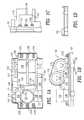
- FIGS. 1A, 1 B, 1 C and IDshow top, side, front and rear end views, respectively, of an adaptable planar module according to an embodiment of the invention.
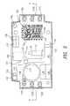
- FIG. 2shows a top view of the module of FIGS. 1A-1D with the IMS exposed.
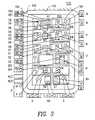
- FIG. 3shows the IMS substrate and its interconnect to the PCB of FIG. 2 in greater detail.
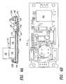
- FIG. 4Ashows a cross-sectional view of the PCB of FIG. 1A taken along lines 4 — 4 .
- FIG. 4Bshows a top view of the PCB.
- FIGS. 5A and 5Bshow a top view and a cross-sectional view, respectively, of an adaptable planar module according to a further embodiment of the invention.
- FIGS. 6A and 6Brespectively show a top view and a cross-sectional view, of a micro-inverter module according to another aspect of the invention.
- FIGS. 7A and 7Bshow a top view and a cross-sectional view, respectively, of a micro-inverter module according to still further embodiment of the invention.
- FIGS. 8A and 8Bshow a top view and cross-sectional view, respectively, of a micro-inverter module according to yet another embodiment of the invention.
- FIGS. 9A and 9Bshow respective top and cross-sectional views of an adaptable planar module according to another embodiment of the invention.
- FIGS. 10A and 10Bshow a top view and a cross-sectional view, respectively, of an adaptable planar module according to still further embodiment of the invention.
- FIG. 11shows a top view of an adaptable planar module according to an additional embodiment of the invention.
- FIG. 12shows a top view of a further arrangement of an IMS according to the invention.
- FIGS. 13A and 13Bshow respective top and side views of an example of a 1 ⁇ 2 HP motor control module which is capable of housing the IMS of FIG. 13 .
- FIG. 14is a cross-sectional view of an embodiment of a semiconductor device module according to the present invention.
- FIG. 15is a cross-sectional view of an embodiment of a semiconductor device module according to the present invention that includes a heatsink with a raised platform below the thermally conductive substrate.
- FIG. 16is a cross-sectional view of an embodiment of a semiconductor device module according to the present invention that includes a heatsink with a raised platform, similar to the module in FIG. 2, and further showing electrical connection between a semiconductor device and PCB components by electrical contacts provided on the top side of the substrate and the bottom side of the PCB.
- FIG. 17shows a cross-sectional view of an embodiment of a semiconductor device module according to the present invention in which a PCB is shown mounted over the substrate, and the semiconductor devices are electrically connected to the PCB components by vias.
- FIG. 18is a cross-sectional view of a semiconductor device module including a shell for supporting a substrate and a PCB to provide a module, which is then mounted on a heatsink as shown.
- FIG. 18Ais a cross-sectional view of a semiconductor device module of FIG. 5 further showing a support structure for supporting capacitors atop a cover.
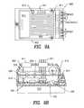
- FIGS. 1A-1Dan APM 100 according to an embodiment of the invention.
- the APMincludes a support base 102 which supports a printed circuit board 110 .
- Mounted atop printed circuit board 110are various electrical components including choke 124 , resistors 130 , 131 , 132 , 133 , 134 , capacitors 136 , 138 , transformer 148 , inductors 141 and 146 as well as additional circuit elements 140 , 142 and 144 and other components, all of which are interconnected by printed wiring (not shown) on circuit board 110 .
- I/O pins 127 and 129 and terminals 122 A- 122 Fwhich provide external connections to the circuit board.
- a support tray 131rests atop circuit board 110 and supports capacitors 126 and 128 which are electrically connected to circuit board 110 and which are held in place by belt 130 .
- FIG. 2shows the top view shown in FIG. 1A of APM 100 but with the support tray and its capacitors removed.
- An opening 160 formed in circuit board 110is situated above an IMS 150 .
- Bonding pads 164are arranged around the periphery of opening 160 and are electrically connected to the other components mounted on the board.
- Bonding wires 156provide electrical connections between the bonding pads 164 of the circuit board and the components mounted on IMS 150 .
- FIG. 3shows the top view of the IMS as well as a portion of the circuit board 110 that surrounds opening 160 in greater detail.
- IMS 150Mounted atop IMS 150 are various components including MOS-gate controlled power semiconductor devices Q 1 -Q 6 , diodes D 1 -D 10 as well as resistors RT and RS 1 . Each of these components are thermally and electrically mounted atop portions of a conducting patterned material 154 , such as copper. Also present, on the top surfaces of the devices, are bonding pad areas. Bonding wires 156 provide connections from the various components as well as from bonding pads 164 to the conducting pattern and the pad areas of the IMS components.
- FIG. 4Aillustrates a cross-sectional view of the structure of FIG. 2 .
- the IMShas a relatively thick body 152 formed of a conductive metal, such as aluminum, that is covered by a very thin insulation layer which, in turn, carries the conductive pattern which is electrically insulated from the body. Also present are heat spreaders (not shown) to which the components are mounted for improving thermal management of the heat generated by the components during their operation.
- An example of an IMSis described in the above-mentioned U.S. Pat. No. 5,408,128, which is incorporated herein by reference.
- the IMSis mounted in an opening of the support body 102 such that it is situated below the circuit board 110 and such that the bottom surface of the body 152 is located co-planar with or below the bottom surface 104 of support body 102 and is available for thermal contact with a heatsink (not shown).
- a heatsink(not shown).
- raised portions 106 and 108which extends from support body 102 and support the circuit board 110 at the opening and periphery, respectively, of the circuit board 110 .
- the raised portions 106 and the opening in the circuit boardform a cavity above the IMS which is filled with a high grade potting material 158 to cover the top surface of the IMS.
- a lower grade, and less costly, potting materialcan then be used between the bottom surface of the circuit board and the support body as well as to cover at least a portion of the components mounted atop the circuit board.
- FIG. 4Bshows an example of a circuit board 210 which is suitable for mounting components as well as having an opening 260 that is to be situated above the IMS and employed in the manner of the invention.
- the arrangement of the opening in the circuit board above the IMSminimizes the number and the length of the bonding wires that connect the components mounted atop the IMS and those mounted on the circuit board. Moreover, by mounting only the high power components on the IMS, the cost of the module is greatly reduced. Further, because both the high power and low power components are mounted in the same module, the footprint is greatly reduced, and the number of interconnections is further decreased. Additionally, by limiting the high grade potting compound to only the region atop the IMS, the cost of the module is also reduced.
- a coversuch as a molded cover, (not shown) may be supplied atop the circuit board to cover the components of the circuit board and the IMS and is preferably supported by the periphery of the support base.
- FIGS. 5A and 5Bshow an example of appliance APM package 500 with no input/output filters in accordance with another embodiment of the invention.
- a molded shell support base 502supports a printed circuit board 510 and has an opening through which IMS 550 is mounted. The bottom surface of the IMS 550 contacts heatsink 570 to remove heat from the power devices mounted atop the IMS, as described above. Also, an opening 560 formed in the circuit board is situated atop the IMS to minimize the length of the wire bonds.
- a high grade potting material 558fills a cavity region above the IMS, and a lower grade potting material 559 is present elsewhere in the module. It should also be noted that components 528 are mounted both on the top and bottom surfaces of the module.
- the terminals 522are fast-on connectors with in-line connector pins for providing control signals. Also shown are optional input/output pins 524 .
- the typically 3.0′′ ⁇ 2.0′′ ⁇ 0.5′′ packagecan house a full motor control circuit, including an inverter circuit, input circuits, protection circuits and a microprocessor.
- the inverter and input circuits 512are located on the IMS 550 , and other components 528 are located on the circuit board 510 .
- the 3.0 inch lengthis a protective maximum size, though streamlined products may be smaller in size.
- FIGS. 6A and 6Bshow an example of a micro-inverter APM package 600 with full input/output filters according to a further embodiment of the invention.
- This embodimentis similar to the appliance APM 500 except that an additional printed circuit board 640 is added for supporting the inductors and capacitors of the input/output filters.
- the added board 640is connected to board 610 by interconnect lead frame 615 .
- the size of the added board and its componentswill vary with power rating of the APM, which ranges typically between 0.1 to 1.0 HP.
- FIGS. 6A and 6Bshow a simple shell with procured terminals 622 .
- FIG. 7A and 7Bshow a substantially similar APM 700 with a shell 702 and integrated terminals 722 . Note that with the procured terminals or the integrated terminals, the terminals are soldered to the main PCB with an isolated potting cavity. Optional input/output pins 624 are also shown.
- FIGS. 8A and 8Bshow an example of a micro-inverter APM package 800 with no filters in accordance with a still further embodiment of the invention.
- the packageis similar to that of FIGS. 6A-6B and 7 A- 7 B except the body height is reduced by the elimination of the added circuit board that otherwise holds the filter circuit. Instead, a buss capacitor 826 is mounted below the bottom surface of the base 802 but away from heatsink 870 .
- FIGS. 8A and 8Bshow integrated shell terminals 822 , the procured terminals are also an option.
- the APM packages of FIGS. 6A-6B, 7 A- 7 B and 8 A- 8 Bcan also be modified to accommodate a keyboard 612 , 712 or 812 , respectively, on the top surface of the PCB.
- the packagescan also accommodate a lid which may provide EMI shielding.
- the filtering and package of the inventionare designed to minimize filter size and have an architecture such that common tooling and processing can be used where possible for more than one embodiment of the APM.
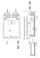
- FIGS. 9A and 9Bshow top and cross-sectional views of an embodiment of a complete motor drive APM 900 with integrated terminals 922 in further accordance with the invention.
- a molded cover lid 904is shown which includes an input/output connector 921 , LED 913 and air vents 917 .
- FIGS. 10A-10Bshow another example of a top and cross-sectional views of a complete motor drive APM 901 with attached terminals 982 according to another embodiment of the invention.
- the attached terminals 982are substituted in place of integrated terminals 922 shown in FIGS. 9A-9B.
- FIG. 11shows a top view of another embodiment of a complete motor drive APM 1103 in accordance with the invention.
- integrated terminals 1122 A and 1122 Bare located at opposite ends of the package.
- FIG. 12shows a further example of an IMS 1250 comprised of plural transistors, IGBTs, diodes and resistors which are interconnected as well as externally connected.
- FIGS. 13A and 13Billustrate an embodiment of a 1 ⁇ 2 HP motor control module and drive circuit APM module 1200 which is likewise in accordance with the invention.
- the moduleincludes a driver PCB 1210 and houses an IMS 1250 , such as is shown in FIG. 13, which is connected to the driver PCB.
- a control board 1240may be included in the module and arranged atop the driver circuit board, and a further optional keyboard 1244 may be included and arranged atop the control board.
- the moduleis extended in length so that control circuits may be included on an extended driver PCB 1210 A.
- an extended keyboard 1244 Amay also be included in the module and arranged atop the extended circuit board.
- the novel features of the above embodiment of the APM of the inventionallow these products to be manufactured at lower cost.
- the primary cost reduction featuresinclude: 1) minimized IMS substrate area, 2) a thinner IMS substrate, 3) no wire bonds on the IMS metalization, 3) all tracks on a double side PCB, 4) all substrate-to-IMS connections are wire bonds that are ordinarily otherwise present, 5) an integrated driver and microprocessor printed circuit board, 6) an integrated shell/terminal molding option, 7) a single package for all functions with potting to reduce size and UL creepage path limitations, and 8) compatible tooling for European and U.S. products for both micro-inverter and appliance products.
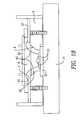
- FIG. 18shows an APM including a thermally conductive substrate 22 that is thermally connected to a heatsink 21 so that the heat that is generated by a semiconductor device 23 residing on the thermally conductive substrate 22 may be withdrawn.
- a shell 5is provided to house the components of the module.
- a cavity 6 in the shellallows the semiconductor device to be electrically connected to a component (not shown) on a PCB 27 , which is mounted on the top side of the shell 5 , by the aid of a bonding wire 40 , that extends through the cavity 6 in the shell and a cavity 7 provided in the PCB 27 .
- the cavity 7 in the PCB and the cavity 6 in the shell 5coincide to allow for the passage of the bonding wire 40 .
- the bonding wire 40is electrically connected at one end to the semiconductor device 23 and at the other end to a bonding pad 55 .
- the bonding pad 55is electrically connected to a component or device on the PCB, thereby allowing electrical communication between the semiconductor device 23 and the component or device. Many bonding pads may be provided as needed.
- the bonding padsmay be disposed along the periphery of the cavity 7 in the PCB 27 on the top side. Multiple electrical connections between multiple semiconductor devices residing on the thermally conductive substrate and various components on the PCB may be made in the same manner.
- a cover 25is provided over the cavity 7 in the PCB 27 to enclose a space 8 over the thermally conductive substrate.
- the enclosed space 8contains a potting compound 50 .
- This modulehas been described in detail in Ser. No. 09/197,078.
- This modulemay be further improved by making the cover 25 from a suitable conductive shielding material or applying a conductive shield to the cover. Conductive shielding will reduce the RFI noise that emanates from the bonding wires.
- the top of the covermay be modified to include features for supporting capacitors.
- the specific embodiment shown in FIG. 18Aincludes a cover 25 A that has been modified to provide support to two capacitors 126 , 128 , a first capacitor 126 and a second capacitor 128 .
- the capacitors 126 , 128are both cylindrically shaped, and rest on their sides above the top side of the cover.
- the first capacitor 126rests upon a first plane, which may be substantially parallel to the plane of the top of the cover.
- the second capacitor 128rests upon a support tray 131 , which supports the second capacitor on a second plane above, and substantially parallel to the first plane.
- This step-like configuration for positioning the capacitorsallows part of the second capacitor to extend outside of the edge of the cover. Further, because the second capacitor is supported above the top face of the cover, an area on the PCB 27 is available under the support tray 131 with sufficient vertical clearance for placement of components on the PCB 27 as shown.
- Two stop members 29 , 28 , a first stop member 29 and a second stop member 28provide lateral support so that the capacitors 126 , 128 will not fall off the cover.
- the first stop member 29prevents the first capacitor 128 from slipping or falling off an edge of the cover; while the second stop member 28 prevents the second capacitor 126 from slipping or falling off an opposite edge on the cover.
- the support tray 131 , the two stop members 28 , 29 , and the coverare of unitary configuration, and are made of a polymer of suitable mechanical, electrical and thermal characteristics.
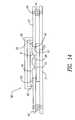
- FIG. 14there is shown an FPA 60 according to the present invention.
- the FPAincludes one or a plurality of semiconductor devices 23 mounted atop a thermally conductive substrate 22 .
- the thermally conductive substrate 22is directly attached to a heat sink 21 .
- a PCB 27is provided above the thermally conductive substrate 22 .
- the PCB 27includes a cavity 10 , which is positioned over the thermally conductive substrate 22 .
- the outer edges on the top side of the thermally conductive substrate 22are attached by double sided adhesive tape 43 or other suitable means to the underside of the PCB 27 along the under-edges of the cavity 10 such that the cavity 10 is closed by the thermally conductive substrate 22 .
- a bonding pad 55is disposed on the periphery of the cavity on the top side of the PCB 27 , and is connected to at least one device (not shown) on the PCB 27 .
- Bonding wire 40electrically connects the semiconductor device 23 to the bonding pad 55 , thereby placing the semiconductor device in electrical communication with the device on the PCB.
- another semiconductor device 24which is in electrical communication with a device (not shown) on the PCB 27 by a bonding wire 41 that is electrically connected to another bonding pad 56 .
- a molded cover 25is placed over the cavity 10 in the PCB 27 to enclose a space over the exposed semiconductor devices.
- a potting compound 50is contained in the space.
- PCB standoffs 42 , 44provide support to the PCB 27 ; while a screw 45 or other appropriate mounting means such as a clip secures the PCB 27 on the heatsink 21 .
- the FPA of FIG. 14eliminates the need for a complex rugged shell, thereby eliminating the cost associated with including such shells in the manufacturing of these modules. Instead, a shell cover made from much cheaper materials may be used. The molded cover may also be manufactured from low strength, low temperature grade material to further reduce the cost of manufacturing.
- the FPA of FIG. 14also requires shorter bonding wires, which results in more reliable and manufacturable electrical bonds between the semiconductor devices and the PCB. Shorter bonding wires also reduce the radiated RFI energy emanating from the bonding wires.
- double sided adhesive tape 43 between the PCB and the thermally conductive substratecan provide suitable insulation for FPAs intended for high voltage application (>42 V) to meet creepage requirements of UL.
- a heatsink 26includes a raised portion, which provides a platform under the thermally conductive substrate 22 .
- the platformmay be made on a basic heatsink by one of many ways such as extrusion, insertion of additional metal, bumping or stamping.
- the PCB 27is placed farther away from the heatsink, thus it is not heated by the heatsink.
- Coating the heatsink with a thermally nonconductive coatingfurther prevents the heatsink from heating the PCB.
- application of an electrically insulating coat 26 A applied or stuck to the heatsinkmay obviate safety concerns.
- the embodiment of the invention as shown in FIG. 15is particularly useful where safety requirements (such as UL and VDE requirements) mandate minimum amount of strike and creepage distances that cannot use the structure that is shown in the embodiment shown in FIG. 14 .
- safety requirementssuch as UL and VDE requirements
- Another advantageous aspect of the FPA shown in FIG. 15is the reduction in the length of the bonding distance as the substrate's top face is closer to the PCB's top face, which reduction as discussed previously reduces the amount RFI.
- the volume of the space created by the molded coveris reduce, thus requiring less potting compound, which in turn reduces the cost of manufacturing the FPA.
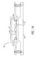
- FIG. 16Another embodiment of an FPA 80 in accord with the invention is shown in FIG. 16 .
- an FPAincluding a heatsink 26 having a platform under a thermally conductive substrate 22 .
- An electrical contact pad 71is provided on the substrate, which is in electrical communication with a semiconductor device 23 through a bonding wire 40 .
- the bonding wiremay be electrically connected to an electrical bonding pad residing on the substrate 22 which is electrically connected to the electrical contact pad 71 .
- Another electrical contact pad 70is provided on the PCB 27 , which contact is electrically connected to another device (not shown) on the PCB 27 .
- the electrical contact pad 70 on the PCB and electrical contact pad 71 on the thermally conductive substrateare in touch to provide electrical communication between a semiconductor device 23 and a device (not shown) on the PCB 27 .
- Such a configurationadvantageously allows for the testing of the semiconductor devices before assembly, thus reducing the number of rejected products during the manufacturing, which in turn provides cost savings.
- FIG. 17illustrates yet another embodiment of an FPA 90 according to the present invention.
- a PCB 27 Ais positioned above and spaced away from a thermally conductive substrate 22 .
- No cavityis provided in the PCB 27 A.
- An enclosure means 20is lodged between the underside of the PCB 27 A and the top side of the thermally conductive substrate 22 .
- the enclosure means 20encloses a space above the thermally conductive substrate 22 , which space contains a suitable potting compound 50 .
- the enclosure meansis made from a suitable insulating material.
- a bonding wire 40that is electrically connected to the semiconductor device 23 at one end, and in electrical communication with a via, for example via 30 , at the other end, thus provides electrical communication between the semiconductor device 23 and the device 15 or other devices on the PCB 27 A.
- the embodiment of the invention according to FIG. 17eliminates the need for a molded cover.
- the elimination of the cavity from the PCBprovides for more surface area on the PCB for mounting devices or components, thereby allowing smaller modules to be constructed according to the present invention.
Landscapes
- Engineering & Computer Science (AREA)
- Microelectronics & Electronic Packaging (AREA)
- Physics & Mathematics (AREA)
- Computer Hardware Design (AREA)
- General Physics & Mathematics (AREA)
- Condensed Matter Physics & Semiconductors (AREA)
- Power Engineering (AREA)
- Chemical & Material Sciences (AREA)
- Dispersion Chemistry (AREA)
- Thermal Sciences (AREA)
- Cooling Or The Like Of Electrical Apparatus (AREA)
- Inverter Devices (AREA)
- Cooling Or The Like Of Semiconductors Or Solid State Devices (AREA)
Abstract
Description
Claims (30)
Priority Applications (1)
| Application Number | Priority Date | Filing Date | Title |
|---|---|---|---|
| US09/709,883US6362964B1 (en) | 1999-11-17 | 2000-11-09 | Flexible power assembly |
Applications Claiming Priority (2)
| Application Number | Priority Date | Filing Date | Title |
|---|---|---|---|
| US16614899P | 1999-11-17 | 1999-11-17 | |
| US09/709,883US6362964B1 (en) | 1999-11-17 | 2000-11-09 | Flexible power assembly |
Publications (1)
| Publication Number | Publication Date |
|---|---|
| US6362964B1true US6362964B1 (en) | 2002-03-26 |
Family
ID=22602021
Family Applications (1)
| Application Number | Title | Priority Date | Filing Date |
|---|---|---|---|
| US09/709,883Expired - Fee RelatedUS6362964B1 (en) | 1999-11-17 | 2000-11-09 | Flexible power assembly |
Country Status (4)
| Country | Link |
|---|---|
| US (1) | US6362964B1 (en) |
| JP (2) | JP2001210784A (en) |
| DE (1) | DE10056832B4 (en) |
| FR (2) | FR2801725B1 (en) |
Cited By (59)
| Publication number | Priority date | Publication date | Assignee | Title |
|---|---|---|---|---|
| US6501103B1 (en)* | 2001-10-23 | 2002-12-31 | Lite-On Electronics, Inc. | Light emitting diode assembly with low thermal resistance |
| US6538313B1 (en)* | 2001-11-13 | 2003-03-25 | National Semiconductor Corporation | IC package with integral substrate capacitor |
| US20030132042A1 (en)* | 2002-01-16 | 2003-07-17 | Beihoff Bruce C. | Vehicle drive module having improved terminal design |
| US20030133257A1 (en)* | 2002-01-16 | 2003-07-17 | Beihoff Bruce C. | Modular power converter having fluid cooled support |
| US20030132041A1 (en)* | 2002-01-16 | 2003-07-17 | Beihoff Bruce C. | Fluid cooled vehicle drive module |
| US20030133283A1 (en)* | 2002-01-16 | 2003-07-17 | Beihoff Bruce C. | Vehicle drive module having improved EMI shielding |
| US20030133259A1 (en)* | 2002-01-16 | 2003-07-17 | Meyer Andreas A. | Compact vehicle drive module having improved thermal control |
| US20030133282A1 (en)* | 2002-01-16 | 2003-07-17 | Beihoff Bruce C. | Power converter having improved EMI shielding |
| US20030132040A1 (en)* | 2002-01-16 | 2003-07-17 | Radosevich Lawrence D. | Vehicle drive module having improved cooling configuration |
| US20030153128A1 (en)* | 2002-02-06 | 2003-08-14 | Hitachi, Ltd. | Semiconductor device and manufacturing the same |
| US20030151893A1 (en)* | 2002-01-16 | 2003-08-14 | Meyer Andreas A. | Power converter having improved fluid cooling |
| US20030178731A1 (en)* | 2000-03-07 | 2003-09-25 | Rumsey Brad D. | Partial slot cover for encapsulation process |
| US20030227730A1 (en)* | 2002-04-24 | 2003-12-11 | Junichi Iimura | Inverted circuit overcurrent protection device and hybrid integrated circuit device with the same incorporated |
| US20040008532A1 (en)* | 2002-07-09 | 2004-01-15 | Izumi Products Company | Power supply device |
| US20040079957A1 (en)* | 2002-09-04 | 2004-04-29 | Andrews Peter Scott | Power surface mount light emitting die package |
| US20040155645A1 (en)* | 2003-02-10 | 2004-08-12 | Siemens Vdo Automotive Inc. | Jump bar shunt structure for power components |
| US20040228097A1 (en)* | 2003-05-14 | 2004-11-18 | Cyntec Co., Ltd. | Construction for high density power module package |
| US20050018386A1 (en)* | 2002-01-16 | 2005-01-27 | Beihoff Bruce C. | Cooled electrical terminal assembly and device incorporating same |
| US20060131601A1 (en)* | 2004-12-21 | 2006-06-22 | Ouderkirk Andrew J | Illumination assembly and method of making same |
| US20060131602A1 (en)* | 2004-12-21 | 2006-06-22 | Ouderkirk Andrew J | Illumination assembly and method of making same |
| US20060131596A1 (en)* | 2004-12-21 | 2006-06-22 | Ouderkirk Andrew J | Illumination assembly and method of making same |
| US20060145339A1 (en)* | 2005-01-05 | 2006-07-06 | Jun Young Yang | Semiconductor package |
| US7116557B1 (en)* | 2003-05-23 | 2006-10-03 | Sti Electronics, Inc. | Imbedded component integrated circuit assembly and method of making same |
| US20060252179A1 (en)* | 2005-05-06 | 2006-11-09 | Neobulb Technologies, Inc. | Integrated circuit packaging structure and method of making the same |
| US7187568B2 (en) | 2002-01-16 | 2007-03-06 | Rockwell Automation Technologies, Inc. | Power converter having improved terminal structure |
| US20070138497A1 (en)* | 2003-05-27 | 2007-06-21 | Loh Ban P | Power surface mount light emitting die package |
| US20070139895A1 (en)* | 2005-11-04 | 2007-06-21 | Reis Bradley E | LED with integral thermal via |
| US20070195532A1 (en)* | 2006-02-21 | 2007-08-23 | Cml Innovative Technologies, Inc. | LED lamp module |
| US20090016034A1 (en)* | 2007-07-12 | 2009-01-15 | Continental Automotive Gmbh | Control Device and Method for Producing a Control Device |
| WO2009052761A1 (en)* | 2007-10-19 | 2009-04-30 | Huawei Technologies Co., Ltd. | A pcb device and a method of manufacture thereof |
| US20090140399A1 (en)* | 2007-11-29 | 2009-06-04 | Infineon Technologies Ag | Semiconductor Module with Switching Components and Driver Electronics |
| US20090180262A1 (en)* | 2008-01-11 | 2009-07-16 | Sma Solar Technology Ag | Inverter |
| US20090261597A1 (en)* | 2005-04-14 | 2009-10-22 | Natural Forces, Llc | Reduced Friction Wind Turbine Apparatus and Method |
| US20090303713A1 (en)* | 2008-06-10 | 2009-12-10 | Advanced Optoelectronic Technology, Inc. | Light source device |
| US20100078202A1 (en)* | 2008-09-26 | 2010-04-01 | Siemens Energy, Inc. | Printed Circuit Board for Harsh Environments |
| US20100084760A1 (en)* | 2008-10-07 | 2010-04-08 | Kabushiki Kaisha Toshiba | Semiconductor device and method for manufacturing same |
| US20100117859A1 (en)* | 2004-06-21 | 2010-05-13 | Mitchell David J | Apparatus and Method of Monitoring Operating Parameters of a Gas Turbine |
| US20100207275A1 (en)* | 2001-02-06 | 2010-08-19 | Renesas Technology Corp. | Hybrid integrated circuit device, and method for fabricating the same, and electronic device |
| US7889502B1 (en)* | 2005-11-04 | 2011-02-15 | Graftech International Holdings Inc. | Heat spreading circuit assembly |
| US7980743B2 (en) | 2005-06-14 | 2011-07-19 | Cree, Inc. | LED backlighting for displays |
| US8376069B2 (en)* | 2008-07-29 | 2013-02-19 | Hitachi, Ltd. | Power conversion apparatus and electric vehicle |
| US20130044484A1 (en)* | 2009-09-29 | 2013-02-21 | Liang Meng Plastic Share Co., Ltd. | Illuminating device and method for manufacturing the same |
| US20130241533A1 (en)* | 2012-03-14 | 2013-09-19 | Nvidia Corporation | Circuit board, current-measuring device, and method of measuring a current of a circuit board |
| US20150131230A1 (en)* | 2013-11-14 | 2015-05-14 | Azurewave Technologies, Inc. | Module ic package structure and method for manufacturing the same |
| EP2835823A4 (en)* | 2012-04-02 | 2016-01-20 | Fuji Electric Co Ltd | POWER CONVERTER |
| US9536800B2 (en) | 2013-12-07 | 2017-01-03 | Fairchild Semiconductor Corporation | Packaged semiconductor devices and methods of manufacturing |
| US20170133355A1 (en)* | 2007-06-08 | 2017-05-11 | Cyntec Co., Ltd. | Three-dimensional package structure |
| CN104218018B (en)* | 2014-08-26 | 2017-08-29 | 深圳三星通信技术研究有限公司 | A kind of radio frequency power amplification modules and its assemble method, radio-frequency module, base station |
| US9929669B2 (en)* | 2016-02-24 | 2018-03-27 | Lsis Co., Ltd. | Inverter |
| US20190056186A1 (en)* | 2017-08-16 | 2019-02-21 | Mahle International Gmbh | Cooling device and method for producing the cooling device |
| US10321585B2 (en) | 2008-07-29 | 2019-06-11 | Hitachi, Ltd. | Power conversion apparatus and electric vehicle |
| WO2019115403A1 (en)* | 2017-12-15 | 2019-06-20 | Sma Solar Technology Ag | Inverter |
| US11056416B2 (en)* | 2018-09-05 | 2021-07-06 | Samsung Electronics Co., Ltd. | Semiconductor device and method of manufacturing the same |
| DE102017123109B4 (en) | 2016-11-07 | 2022-06-02 | Liebherr-Elektronik Gmbh | power electronics module |
| DE102020216390A1 (en) | 2020-12-21 | 2022-06-23 | Vitesco Technologies Germany Gmbh | Control module for a vehicle with at least one electric motor |
| DE102020216395A1 (en) | 2020-12-21 | 2022-06-23 | Vitesco Technologies Germany Gmbh | Vehicle control module with plastic casing |
| US20220396154A1 (en)* | 2021-06-14 | 2022-12-15 | Panasonic Intellectual Property Management Co., Ltd. | Vehicle mounted electric power converter |
| CN115885382A (en)* | 2020-08-25 | 2023-03-31 | 西门子股份公司 | Semiconductor module with recess |
| US11778769B2 (en)* | 2015-11-13 | 2023-10-03 | Valeo Siemens Eautomotive France Sas | Housing for an electrical apparatus |
Families Citing this family (11)
| Publication number | Priority date | Publication date | Assignee | Title |
|---|---|---|---|---|
| DE10151153A1 (en)* | 2001-10-19 | 2003-04-30 | Bombardier Transp Gmbh | Device for charging batteries for electric vehicles has converter containing inverter for producing a.c. voltage from step-up device's D.C. output and rectifier coupled via transformer |
| JP2003258141A (en)* | 2002-02-27 | 2003-09-12 | Nec Compound Semiconductor Devices Ltd | Electronic component and its manufacturing method |
| DE102011121823A1 (en)* | 2011-12-21 | 2013-07-11 | Wabco Gmbh | Electronic unit, has circuit board arranged in cavity of housing for carrying electronic parts, and connected to adhesive strip at side that faces towards housing base such that adhesive strip is connected to inner side of housing base |
| DE102013212446A1 (en)* | 2013-06-27 | 2015-01-15 | Zf Friedrichshafen Ag | Electric circuit and method for producing an electrical circuit for driving a load |
| US9853524B2 (en) | 2014-07-29 | 2017-12-26 | Regal Beloit America, Inc. | Motor and controller with isolation members between electrical components and associated method |
| US10368465B2 (en)* | 2017-09-07 | 2019-07-30 | Lear Corporation | Electrical unit |
| DE102019204639A1 (en)* | 2019-04-02 | 2020-10-08 | Zf Friedrichshafen Ag | Air gap formation in an electrical contacting of a circuit board |
| JP2023127605A (en)* | 2022-03-02 | 2023-09-14 | 株式会社Gsユアサ | Semiconductor switch device with terminal cover and power supply system |
| US20240431040A1 (en)* | 2023-06-26 | 2024-12-26 | Deere & Company | Electronic assembly with a compressive electrical connection between a circuit board and housing |
| FR3156989A1 (en) | 2023-12-13 | 2025-06-20 | IFP Energies Nouvelles | Electronic power board |
| DE102024202353A1 (en)* | 2024-03-13 | 2025-09-18 | Volkswagen Aktiengesellschaft | Power module |
Citations (9)
| Publication number | Priority date | Publication date | Assignee | Title |
|---|---|---|---|---|
| US5012386A (en)* | 1989-10-27 | 1991-04-30 | Motorola, Inc. | High performance overmolded electronic package |
| US5408128A (en) | 1993-09-15 | 1995-04-18 | International Rectifier Corporation | High power semiconductor device module with low thermal resistance and simplified manufacturing |
| US5583377A (en)* | 1992-07-15 | 1996-12-10 | Motorola, Inc. | Pad array semiconductor device having a heat sink with die receiving cavity |
| US5663869A (en)* | 1992-07-17 | 1997-09-02 | Vlt Corporation | Packaging electrical components |
| US5670749A (en)* | 1995-09-29 | 1997-09-23 | Allen-Bradley Company, Inc. | Multilayer circuit board having a window exposing an enhanced conductive layer for use as an insulated mounting area |
| US5966291A (en)* | 1996-11-06 | 1999-10-12 | Temic Telefunken Microelectronic Gmbh | Power module for the control of electric motors |
| US6011692A (en)* | 1997-08-25 | 2000-01-04 | Telefonaktiebolaget Lm Ericsson | Chip supporting element |
| US6081426A (en)* | 1996-09-18 | 2000-06-27 | Shinko Electric Industries Co., Ltd. | Semiconductor package having a heat slug |
| US6147869A (en)* | 1997-11-24 | 2000-11-14 | International Rectifier Corp. | Adaptable planar module |
Family Cites Families (11)
| Publication number | Priority date | Publication date | Assignee | Title |
|---|---|---|---|---|
| DE3538933A1 (en)* | 1985-11-02 | 1987-05-14 | Bbc Brown Boveri & Cie | PERFORMANCE SEMICONDUCTOR MODULE |
| EP0420604A1 (en)* | 1989-09-27 | 1991-04-03 | Motorola, Inc. | Selectively conductive adhesive device for simultaneous electrical and mechanical coupling |
| EP0516149B1 (en)* | 1991-05-31 | 1998-09-23 | Denso Corporation | Electronic device |
| JP2854757B2 (en)* | 1992-06-17 | 1999-02-03 | 三菱電機株式会社 | Semiconductor power module |
| DE4418426B4 (en)* | 1993-09-08 | 2007-08-02 | Mitsubishi Denki K.K. | Semiconductor power module and method of manufacturing the semiconductor power module |
| JP3198796B2 (en)* | 1993-06-25 | 2001-08-13 | 富士電機株式会社 | Mold module |
| JPH07263621A (en)* | 1994-03-18 | 1995-10-13 | Toshiba Corp | Semiconductor device |
| JP3466329B2 (en)* | 1995-06-16 | 2003-11-10 | 三菱電機株式会社 | Semiconductor power module |
| JP3322575B2 (en)* | 1996-07-31 | 2002-09-09 | 太陽誘電株式会社 | Hybrid module and manufacturing method thereof |
| FR2758935B1 (en)* | 1997-01-28 | 2001-02-16 | Matra Marconi Space France | MULTI-LEVEL MICRO-ELECTRONIC BOX |
| US5812387A (en)* | 1997-02-21 | 1998-09-22 | International Power Devices, Inc. | Multi-deck power converter module |
- 2000
- 2000-11-09USUS09/709,883patent/US6362964B1/ennot_activeExpired - Fee Related
- 2000-11-16DEDE10056832Apatent/DE10056832B4/ennot_activeExpired - Fee Related
- 2000-11-17FRFR0014866Apatent/FR2801725B1/ennot_activeExpired - Fee Related
- 2000-11-17JPJP2000350726Apatent/JP2001210784A/enactivePending
- 2001
- 2001-05-02FRFR0105872Apatent/FR2809231B1/ennot_activeExpired - Fee Related
- 2007
- 2007-04-16JPJP2007107052Apatent/JP2007227957A/enactivePending
Patent Citations (9)
| Publication number | Priority date | Publication date | Assignee | Title |
|---|---|---|---|---|
| US5012386A (en)* | 1989-10-27 | 1991-04-30 | Motorola, Inc. | High performance overmolded electronic package |
| US5583377A (en)* | 1992-07-15 | 1996-12-10 | Motorola, Inc. | Pad array semiconductor device having a heat sink with die receiving cavity |
| US5663869A (en)* | 1992-07-17 | 1997-09-02 | Vlt Corporation | Packaging electrical components |
| US5408128A (en) | 1993-09-15 | 1995-04-18 | International Rectifier Corporation | High power semiconductor device module with low thermal resistance and simplified manufacturing |
| US5670749A (en)* | 1995-09-29 | 1997-09-23 | Allen-Bradley Company, Inc. | Multilayer circuit board having a window exposing an enhanced conductive layer for use as an insulated mounting area |
| US6081426A (en)* | 1996-09-18 | 2000-06-27 | Shinko Electric Industries Co., Ltd. | Semiconductor package having a heat slug |
| US5966291A (en)* | 1996-11-06 | 1999-10-12 | Temic Telefunken Microelectronic Gmbh | Power module for the control of electric motors |
| US6011692A (en)* | 1997-08-25 | 2000-01-04 | Telefonaktiebolaget Lm Ericsson | Chip supporting element |
| US6147869A (en)* | 1997-11-24 | 2000-11-14 | International Rectifier Corp. | Adaptable planar module |
Cited By (129)
| Publication number | Priority date | Publication date | Assignee | Title |
|---|---|---|---|---|
| US20030178731A1 (en)* | 2000-03-07 | 2003-09-25 | Rumsey Brad D. | Partial slot cover for encapsulation process |
| US6984894B2 (en)* | 2000-03-07 | 2006-01-10 | Micron Technology, Inc. | Semiconductor package having a partial slot cover for encapsulation process |
| US8581395B2 (en) | 2001-02-06 | 2013-11-12 | Renesas Electronics Corporation | Hybrid integrated circuit device and electronic device |
| US8222734B2 (en) | 2001-02-06 | 2012-07-17 | Renesas Electronics Corporation | Hybrid integrated circuit device and electronic device |
| US8084852B2 (en) | 2001-02-06 | 2011-12-27 | Renesas Electronics Corporation | Hybrid integrated circuit device, and method for fabricating the same, and electronic device |
| US20110121365A1 (en)* | 2001-02-06 | 2011-05-26 | Renesas Electronics Corporation | Hybrid integrated circuit device, and method for fabricating the same, and electronic device |
| US7902656B2 (en)* | 2001-02-06 | 2011-03-08 | Renesas Electronics Corporation | Hybrid integrated circuit device, and method for fabricating the same, and electronic device |
| US20100207275A1 (en)* | 2001-02-06 | 2010-08-19 | Renesas Technology Corp. | Hybrid integrated circuit device, and method for fabricating the same, and electronic device |
| US6501103B1 (en)* | 2001-10-23 | 2002-12-31 | Lite-On Electronics, Inc. | Light emitting diode assembly with low thermal resistance |
| US6538313B1 (en)* | 2001-11-13 | 2003-03-25 | National Semiconductor Corporation | IC package with integral substrate capacitor |
| US20050002162A1 (en)* | 2002-01-16 | 2005-01-06 | Beihoff Bruce C. | Modular power converter having fluid cooled support |
| US6982873B2 (en) | 2002-01-16 | 2006-01-03 | Rockwell Automation Technologies, Inc. | Compact vehicle drive module having improved thermal control |
| US20030132042A1 (en)* | 2002-01-16 | 2003-07-17 | Beihoff Bruce C. | Vehicle drive module having improved terminal design |
| US7142434B2 (en) | 2002-01-16 | 2006-11-28 | Rockwell Automation Technologies, Inc. | Vehicle drive module having improved EMI shielding |
| US7187568B2 (en) | 2002-01-16 | 2007-03-06 | Rockwell Automation Technologies, Inc. | Power converter having improved terminal structure |
| US20040066643A1 (en)* | 2002-01-16 | 2004-04-08 | Beihoff Bruce C. | Power converter having improved EMI shielding |
| US7187548B2 (en)* | 2002-01-16 | 2007-03-06 | Rockwell Automation Technologies, Inc. | Power converter having improved fluid cooling |
| US7095612B2 (en) | 2002-01-16 | 2006-08-22 | Rockwell Automation Technologies, Inc. | Cooled electrical terminal assembly and device incorporating same |
| US20030132040A1 (en)* | 2002-01-16 | 2003-07-17 | Radosevich Lawrence D. | Vehicle drive module having improved cooling configuration |
| US20030133282A1 (en)* | 2002-01-16 | 2003-07-17 | Beihoff Bruce C. | Power converter having improved EMI shielding |
| US7177153B2 (en)* | 2002-01-16 | 2007-02-13 | Rockwell Automation Technologies, Inc. | Vehicle drive module having improved cooling configuration |
| US20050018386A1 (en)* | 2002-01-16 | 2005-01-27 | Beihoff Bruce C. | Cooled electrical terminal assembly and device incorporating same |
| US20050088835A9 (en)* | 2002-01-16 | 2005-04-28 | Beihoff Bruce C. | Vehicle drive module having improved EMI shielding |
| US6972957B2 (en) | 2002-01-16 | 2005-12-06 | Rockwell Automation Technologies, Inc. | Modular power converter having fluid cooled support |
| US20030133259A1 (en)* | 2002-01-16 | 2003-07-17 | Meyer Andreas A. | Compact vehicle drive module having improved thermal control |
| US20030151893A1 (en)* | 2002-01-16 | 2003-08-14 | Meyer Andreas A. | Power converter having improved fluid cooling |
| US20030133283A1 (en)* | 2002-01-16 | 2003-07-17 | Beihoff Bruce C. | Vehicle drive module having improved EMI shielding |
| US7016192B2 (en) | 2002-01-16 | 2006-03-21 | Rockwell Automation Technologies, Inc. | Electrical power converter method and system employing multiple-output converters |
| US7032695B2 (en) | 2002-01-16 | 2006-04-25 | Rockwell Automation Technologies, Inc. | Vehicle drive module having improved terminal design |
| US20060092611A1 (en)* | 2002-01-16 | 2006-05-04 | Beihoff Bruce C | Electrical power converter method and system employing multiple output converters |
| US7061775B2 (en) | 2002-01-16 | 2006-06-13 | Rockwell Automation Technologies, Inc. | Power converter having improved EMI shielding |
| US7450388B2 (en) | 2002-01-16 | 2008-11-11 | Rockwell Automation Technologies, Inc. | Power converter connection configuration |
| US20030132041A1 (en)* | 2002-01-16 | 2003-07-17 | Beihoff Bruce C. | Fluid cooled vehicle drive module |
| US20030133257A1 (en)* | 2002-01-16 | 2003-07-17 | Beihoff Bruce C. | Modular power converter having fluid cooled support |
| US7212407B2 (en) | 2002-01-16 | 2007-05-01 | Rockwell Automation Technologies, Inc. | Electrical power converter method and system employing multiple output converters |
| US20030153128A1 (en)* | 2002-02-06 | 2003-08-14 | Hitachi, Ltd. | Semiconductor device and manufacturing the same |
| US6703261B2 (en)* | 2002-02-06 | 2004-03-09 | Hitachi, Ltd. | Semiconductor device and manufacturing the same |
| US7609498B2 (en) | 2002-04-24 | 2009-10-27 | Sanyo Electric Co., Ltd. | Inverted circuit overcurrent protection device and hybrid integrated circuit device with the same incorporated |
| US7136269B2 (en)* | 2002-04-24 | 2006-11-14 | Sanyo Electric Co., Ltd. | Inverted circuit overcurrent protection device and hybrid integrated circuit device with the same incorporated |
| US20070014065A1 (en)* | 2002-04-24 | 2007-01-18 | Sanyo Electric Co., Ltd. | Inverted circuit overcurrent protection device and hybrid integrated circuit device with the same incorporated |
| US20030227730A1 (en)* | 2002-04-24 | 2003-12-11 | Junichi Iimura | Inverted circuit overcurrent protection device and hybrid integrated circuit device with the same incorporated |
| US20040008532A1 (en)* | 2002-07-09 | 2004-01-15 | Izumi Products Company | Power supply device |
| US8710514B2 (en) | 2002-09-04 | 2014-04-29 | Cree, Inc. | Power surface mount light emitting die package |
| US20110121345A1 (en)* | 2002-09-04 | 2011-05-26 | Peter Scott Andrews | Power surface mount light emitting die package |
| US20040079957A1 (en)* | 2002-09-04 | 2004-04-29 | Andrews Peter Scott | Power surface mount light emitting die package |
| US8622582B2 (en) | 2002-09-04 | 2014-01-07 | Cree, Inc. | Power surface mount light emitting die package |
| US8608349B2 (en) | 2002-09-04 | 2013-12-17 | Cree, Inc. | Power surface mount light emitting die package |
| US8530915B2 (en) | 2002-09-04 | 2013-09-10 | Cree, Inc. | Power surface mount light emitting die package |
| US7244965B2 (en)* | 2002-09-04 | 2007-07-17 | Cree Inc, | Power surface mount light emitting die package |
| US20110186897A1 (en)* | 2002-09-04 | 2011-08-04 | Loh Ban P | Power surface mount light emitting die package |
| US8167463B2 (en) | 2002-09-04 | 2012-05-01 | Cree, Inc. | Power surface mount light emitting die package |
| US6781360B1 (en)* | 2003-02-10 | 2004-08-24 | Siemens Vdo Automotive Inc. | Jump bar shunt structure for power components |
| US20040155645A1 (en)* | 2003-02-10 | 2004-08-12 | Siemens Vdo Automotive Inc. | Jump bar shunt structure for power components |
| US20040228097A1 (en)* | 2003-05-14 | 2004-11-18 | Cyntec Co., Ltd. | Construction for high density power module package |
| US6975513B2 (en)* | 2003-05-14 | 2005-12-13 | Cyntec Co., Ltd. | Construction for high density power module package |
| US7116557B1 (en)* | 2003-05-23 | 2006-10-03 | Sti Electronics, Inc. | Imbedded component integrated circuit assembly and method of making same |
| US7976186B2 (en) | 2003-05-27 | 2011-07-12 | Cree, Inc. | Power surface mount light emitting die package |
| US8188488B2 (en) | 2003-05-27 | 2012-05-29 | Cree, Inc. | Power surface mount light emitting die package |
| US20070138497A1 (en)* | 2003-05-27 | 2007-06-21 | Loh Ban P | Power surface mount light emitting die package |
| US20100301372A1 (en)* | 2003-05-27 | 2010-12-02 | Cree, Inc. | Power surface mount light emitting die package |
| US20070200127A1 (en)* | 2003-05-27 | 2007-08-30 | Andrews Peter S | Power surface mount light emitting die package |
| US7775685B2 (en) | 2003-05-27 | 2010-08-17 | Cree, Inc. | Power surface mount light emitting die package |
| US20100117859A1 (en)* | 2004-06-21 | 2010-05-13 | Mitchell David J | Apparatus and Method of Monitoring Operating Parameters of a Gas Turbine |
| US8742944B2 (en) | 2004-06-21 | 2014-06-03 | Siemens Energy, Inc. | Apparatus and method of monitoring operating parameters of a gas turbine |
| US20060131602A1 (en)* | 2004-12-21 | 2006-06-22 | Ouderkirk Andrew J | Illumination assembly and method of making same |
| US20060131601A1 (en)* | 2004-12-21 | 2006-06-22 | Ouderkirk Andrew J | Illumination assembly and method of making same |
| US7285802B2 (en) | 2004-12-21 | 2007-10-23 | 3M Innovative Properties Company | Illumination assembly and method of making same |
| US7296916B2 (en)* | 2004-12-21 | 2007-11-20 | 3M Innovative Properties Company | Illumination assembly and method of making same |
| US20060131596A1 (en)* | 2004-12-21 | 2006-06-22 | Ouderkirk Andrew J | Illumination assembly and method of making same |
| US7166917B2 (en)* | 2005-01-05 | 2007-01-23 | Advanced Semiconductor Engineering Inc. | Semiconductor package having passive component disposed between semiconductor device and substrate |
| US20060145339A1 (en)* | 2005-01-05 | 2006-07-06 | Jun Young Yang | Semiconductor package |
| US20090261597A1 (en)* | 2005-04-14 | 2009-10-22 | Natural Forces, Llc | Reduced Friction Wind Turbine Apparatus and Method |
| US7847428B2 (en) | 2005-04-14 | 2010-12-07 | Natural Forces, Llc | Reduced friction wind turbine apparatus and method |
| US7948767B2 (en) | 2005-05-06 | 2011-05-24 | Neobulb Technologies, LLP. | Integrated circuit packaging structure and method of making the same |
| US20100140791A1 (en)* | 2005-05-06 | 2010-06-10 | Neobulb Technologies, Inc. | Integrated circuit packaging structure and method of making the same |
| US20060252179A1 (en)* | 2005-05-06 | 2006-11-09 | Neobulb Technologies, Inc. | Integrated circuit packaging structure and method of making the same |
| US7980743B2 (en) | 2005-06-14 | 2011-07-19 | Cree, Inc. | LED backlighting for displays |
| US8308331B2 (en) | 2005-06-14 | 2012-11-13 | Cree, Inc. | LED backlighting for displays |
| US20070139895A1 (en)* | 2005-11-04 | 2007-06-21 | Reis Bradley E | LED with integral thermal via |
| US7889502B1 (en)* | 2005-11-04 | 2011-02-15 | Graftech International Holdings Inc. | Heat spreading circuit assembly |
| US7505275B2 (en)* | 2005-11-04 | 2009-03-17 | Graftech International Holdings Inc. | LED with integral via |
| US20070195532A1 (en)* | 2006-02-21 | 2007-08-23 | Cml Innovative Technologies, Inc. | LED lamp module |
| US7488097B2 (en)* | 2006-02-21 | 2009-02-10 | Cml Innovative Technologies, Inc. | LED lamp module |
| US10593656B2 (en)* | 2007-06-08 | 2020-03-17 | Cyntec Co., Ltd | Three-dimensional package structure |
| US10991681B2 (en)* | 2007-06-08 | 2021-04-27 | Cyntec Co., Ltd. | Three-dimensional package structure |
| US20170133355A1 (en)* | 2007-06-08 | 2017-05-11 | Cyntec Co., Ltd. | Three-dimensional package structure |
| US8031473B2 (en)* | 2007-07-12 | 2011-10-04 | Continental Automotive Gmbh | Control device and method for producing a control device |
| US20090016034A1 (en)* | 2007-07-12 | 2009-01-15 | Continental Automotive Gmbh | Control Device and Method for Producing a Control Device |
| WO2009052761A1 (en)* | 2007-10-19 | 2009-04-30 | Huawei Technologies Co., Ltd. | A pcb device and a method of manufacture thereof |
| US7800222B2 (en)* | 2007-11-29 | 2010-09-21 | Infineon Technologies Ag | Semiconductor module with switching components and driver electronics |
| US20090140399A1 (en)* | 2007-11-29 | 2009-06-04 | Infineon Technologies Ag | Semiconductor Module with Switching Components and Driver Electronics |
| US20090180262A1 (en)* | 2008-01-11 | 2009-07-16 | Sma Solar Technology Ag | Inverter |
| US7985006B2 (en)* | 2008-06-10 | 2011-07-26 | Advanced Optoelectronic Technology, Inc. | Light source device |
| US20090303713A1 (en)* | 2008-06-10 | 2009-12-10 | Advanced Optoelectronic Technology, Inc. | Light source device |
| US10178780B2 (en) | 2008-07-29 | 2019-01-08 | Hitachi, Ltd. | Power conversion apparatus and electric vehicle |
| US9095079B2 (en) | 2008-07-29 | 2015-07-28 | Hitachi, Ltd. | Power conversion apparatus and electric vehicle |
| US9888591B2 (en) | 2008-07-29 | 2018-02-06 | Hitachi, Ltd. | Power conversion apparatus and electric vehicle |
| US10321585B2 (en) | 2008-07-29 | 2019-06-11 | Hitachi, Ltd. | Power conversion apparatus and electric vehicle |
| US11089702B2 (en) | 2008-07-29 | 2021-08-10 | Hitachi, Ltd. | Power conversion apparatus and electric vehicle |
| US8376069B2 (en)* | 2008-07-29 | 2013-02-19 | Hitachi, Ltd. | Power conversion apparatus and electric vehicle |
| US8863869B2 (en) | 2008-07-29 | 2014-10-21 | Hitachi, Ltd. | Power conversion apparatus and electric vehicle |
| US20100078202A1 (en)* | 2008-09-26 | 2010-04-01 | Siemens Energy, Inc. | Printed Circuit Board for Harsh Environments |
| US8076587B2 (en) | 2008-09-26 | 2011-12-13 | Siemens Energy, Inc. | Printed circuit board for harsh environments |
| US8278744B2 (en)* | 2008-10-07 | 2012-10-02 | Kabushiki Kaisha Toshiba | Semiconductor device and method for manufacturing same |
| US20100084760A1 (en)* | 2008-10-07 | 2010-04-08 | Kabushiki Kaisha Toshiba | Semiconductor device and method for manufacturing same |
| US8678617B2 (en)* | 2009-09-29 | 2014-03-25 | Liang Meng Plastic Share Co., Ltd. | Illuminating device and method for manufacturing the same |
| US8746926B2 (en)* | 2009-09-29 | 2014-06-10 | Liang Meng Plastic Share Co., Ltd. | Illuminating device and method for manufacturing the same |
| US20130044484A1 (en)* | 2009-09-29 | 2013-02-21 | Liang Meng Plastic Share Co., Ltd. | Illuminating device and method for manufacturing the same |
| US10123408B2 (en)* | 2012-03-14 | 2018-11-06 | Nvidia Corporation | Circuit board, current-measuring device, and method of measuring a current of a circuit board |
| US20130241533A1 (en)* | 2012-03-14 | 2013-09-19 | Nvidia Corporation | Circuit board, current-measuring device, and method of measuring a current of a circuit board |
| EP2835823A4 (en)* | 2012-04-02 | 2016-01-20 | Fuji Electric Co Ltd | POWER CONVERTER |
| US9373556B2 (en)* | 2013-11-14 | 2016-06-21 | Azurewave Technologies, Inc. | Module IC package structure and method for manufacturing the same |
| US20150131230A1 (en)* | 2013-11-14 | 2015-05-14 | Azurewave Technologies, Inc. | Module ic package structure and method for manufacturing the same |
| US9536800B2 (en) | 2013-12-07 | 2017-01-03 | Fairchild Semiconductor Corporation | Packaged semiconductor devices and methods of manufacturing |
| CN104218018B (en)* | 2014-08-26 | 2017-08-29 | 深圳三星通信技术研究有限公司 | A kind of radio frequency power amplification modules and its assemble method, radio-frequency module, base station |
| US11778769B2 (en)* | 2015-11-13 | 2023-10-03 | Valeo Siemens Eautomotive France Sas | Housing for an electrical apparatus |
| US9929669B2 (en)* | 2016-02-24 | 2018-03-27 | Lsis Co., Ltd. | Inverter |
| DE102017123109B4 (en) | 2016-11-07 | 2022-06-02 | Liebherr-Elektronik Gmbh | power electronics module |
| US20190056186A1 (en)* | 2017-08-16 | 2019-02-21 | Mahle International Gmbh | Cooling device and method for producing the cooling device |
| CN111466074A (en)* | 2017-12-15 | 2020-07-28 | 艾思玛太阳能技术股份公司 | Inverter with a voltage regulator |
| WO2019115403A1 (en)* | 2017-12-15 | 2019-06-20 | Sma Solar Technology Ag | Inverter |
| US11522494B2 (en) | 2017-12-15 | 2022-12-06 | Sma Solar Technology Ag | Inverter |
| CN111466074B (en)* | 2017-12-15 | 2024-02-27 | 艾思玛太阳能技术股份公司 | Inverter with a power supply |
| US11056416B2 (en)* | 2018-09-05 | 2021-07-06 | Samsung Electronics Co., Ltd. | Semiconductor device and method of manufacturing the same |
| US11688661B2 (en) | 2018-09-05 | 2023-06-27 | Samsung Electronics Co., Ltd. | Semiconductor device and method of manufacturing the same |
| CN115885382A (en)* | 2020-08-25 | 2023-03-31 | 西门子股份公司 | Semiconductor module with recess |
| DE102020216390A1 (en) | 2020-12-21 | 2022-06-23 | Vitesco Technologies Germany Gmbh | Control module for a vehicle with at least one electric motor |
| DE102020216395A1 (en) | 2020-12-21 | 2022-06-23 | Vitesco Technologies Germany Gmbh | Vehicle control module with plastic casing |
| US20220396154A1 (en)* | 2021-06-14 | 2022-12-15 | Panasonic Intellectual Property Management Co., Ltd. | Vehicle mounted electric power converter |
Also Published As
| Publication number | Publication date |
|---|---|
| DE10056832A1 (en) | 2001-05-31 |
| DE10056832B4 (en) | 2009-11-26 |
| FR2809231A1 (en) | 2001-11-23 |
| FR2801725B1 (en) | 2007-06-29 |
| FR2809231B1 (en) | 2006-01-06 |
| FR2801725A1 (en) | 2001-06-01 |
| JP2001210784A (en) | 2001-08-03 |
| JP2007227957A (en) | 2007-09-06 |
Similar Documents
| Publication | Publication Date | Title |
|---|---|---|
| US6362964B1 (en) | Flexible power assembly | |
| US6147869A (en) | Adaptable planar module | |
| US6762937B2 (en) | Power module | |
| US6031723A (en) | Insulated surface mount circuit board construction | |
| US5907475A (en) | Circuit board system having a mounted board and a plurality of mounting boards | |
| EP1900022B1 (en) | Complete power management system implemented in a single surface mount package | |
| EP1523036A2 (en) | Semiconductor device heat sink package and method | |
| GB2336254A (en) | Power module for a current converter | |
| WO2002078086A2 (en) | Power transistor package with integrated flange for surface mount heat removal | |
| US5475565A (en) | Power distribution lid for IC package | |
| CN216930700U (en) | Power module | |
| KR100433685B1 (en) | Power train splitter for 10 horsepower motor controller | |
| US7719850B2 (en) | Arrangement with an integrated circuit mounted on a bearing means and a power supply module arrangement | |
| CN112968025A (en) | Intelligent power module and manufacturing method thereof | |
| US5504370A (en) | Electronic system circuit package directly supporting components on isolated subsegments | |
| CN106961793A (en) | Electronic module and method for forming packaging structure thereof | |
| US6587346B1 (en) | Combination electrical power distribution and heat dissipating device | |
| CN214848623U (en) | Electric control board | |
| JP2000196011A (en) | Electronic device and manufacturing method thereof | |
| CN113113398B (en) | Electric control panel | |
| EP0804054A1 (en) | Insulated surface mount circuit board construction | |
| KR20140139649A (en) | Intergral terminal frame and power module having the same | |
| JPH0655971A (en) | Electronic direction indicator | |
| JPH0636639Y2 (en) | Power supply module | |
| US20240032184A1 (en) | Improved electronic component package arrangement |
Legal Events
| Date | Code | Title | Description |
|---|---|---|---|
| AS | Assignment | Owner name:INTERNATIONAL RECTIFIER CORPORATION, CALIFORNIA Free format text:ASSIGNMENT OF ASSIGNORS INTEREST;ASSIGNORS:DUBHASHI, AJIT;SIU, STEPHEN NICHOLAS;LIN, HENY W.;AND OTHERS;REEL/FRAME:011588/0426;SIGNING DATES FROM 20001030 TO 20001106 | |
| FPAY | Fee payment | Year of fee payment:4 | |
| AS | Assignment | Owner name:SILICONIX TECHNOLOGY C. V., SINGAPORE Free format text:ASSIGNMENT OF ASSIGNORS INTEREST;ASSIGNOR:INTERNATIONAL RECTIFIER CORPORATION;REEL/FRAME:019658/0714 Effective date:20070418 Owner name:SILICONIX TECHNOLOGY C. V.,SINGAPORE Free format text:ASSIGNMENT OF ASSIGNORS INTEREST;ASSIGNOR:INTERNATIONAL RECTIFIER CORPORATION;REEL/FRAME:019658/0714 Effective date:20070418 | |
| FEPP | Fee payment procedure | Free format text:PAYOR NUMBER ASSIGNED (ORIGINAL EVENT CODE: ASPN); ENTITY STATUS OF PATENT OWNER: LARGE ENTITY | |
| AS | Assignment | Owner name:ASBU HOLDINGS, LLC, COLORADO Free format text:ASSIGNMENT OF ASSIGNORS INTEREST;ASSIGNOR:SILICONIX TECHNOLOGY C.V.;REEL/FRAME:020886/0809 Effective date:20080409 | |
| REMI | Maintenance fee reminder mailed | ||
| LAPS | Lapse for failure to pay maintenance fees | ||
| STCH | Information on status: patent discontinuation | Free format text:PATENT EXPIRED DUE TO NONPAYMENT OF MAINTENANCE FEES UNDER 37 CFR 1.362 | |
| FP | Lapsed due to failure to pay maintenance fee | Effective date:20100326 |