US6362788B1 - Electromagnetic wave transmitter/receiver - Google Patents
Electromagnetic wave transmitter/receiverDownload PDFInfo
- Publication number
- US6362788B1 US6362788B1US09/582,395US58239500AUS6362788B1US 6362788 B1US6362788 B1US 6362788B1US 58239500 AUS58239500 AUS 58239500AUS 6362788 B1US6362788 B1US 6362788B1
- Authority
- US
- United States
- Prior art keywords
- circuit board
- transmission
- reception
- array
- radiating elements
- Prior art date
- Legal status (The legal status is an assumption and is not a legal conclusion. Google has not performed a legal analysis and makes no representation as to the accuracy of the status listed.)
- Expired - Lifetime
Links
- 230000005540biological transmissionEffects0.000claimsabstractdescription58
- 230000005855radiationEffects0.000claimsabstractdescription23
- 230000005284excitationEffects0.000claimsabstractdescription22
- 238000006243chemical reactionMethods0.000claimsdescription13
- 239000000523sampleSubstances0.000claimsdescription6
- 238000003491arrayMethods0.000claimsdescription2
- 239000000758substrateSubstances0.000description10
- 238000005516engineering processMethods0.000description5
- 230000002452interceptive effectEffects0.000description4
- 238000000034methodMethods0.000description3
- 239000004809TeflonSubstances0.000description2
- 229920006362Teflon®Polymers0.000description2
- 239000004020conductorSubstances0.000description2
- 230000005684electric fieldEffects0.000description2
- 239000006260foamSubstances0.000description2
- 230000010287polarizationEffects0.000description2
- 239000004793PolystyreneSubstances0.000description1
- 239000000654additiveSubstances0.000description1
- 230000000996additive effectEffects0.000description1
- 230000002457bidirectional effectEffects0.000description1
- 239000000919ceramicSubstances0.000description1
- 230000008878couplingEffects0.000description1
- 238000010168coupling processMethods0.000description1
- 238000005859coupling reactionMethods0.000description1
- 238000005388cross polarizationMethods0.000description1
- 239000011521glassSubstances0.000description1
- 238000005286illuminationMethods0.000description1
- 238000002955isolationMethods0.000description1
- 239000000463materialSubstances0.000description1
- 239000002184metalSubstances0.000description1
- 230000010363phase shiftEffects0.000description1
- 229920002223polystyrenePolymers0.000description1
- 238000011144upstream manufacturingMethods0.000description1
Images
Classifications
- H—ELECTRICITY
- H01—ELECTRIC ELEMENTS
- H01Q—ANTENNAS, i.e. RADIO AERIALS
- H01Q21/00—Antenna arrays or systems
- H01Q21/30—Combinations of separate antenna units operating in different wavebands and connected to a common feeder system
- H—ELECTRICITY
- H01—ELECTRIC ELEMENTS
- H01Q—ANTENNAS, i.e. RADIO AERIALS
- H01Q13/00—Waveguide horns or mouths; Slot antennas; Leaky-waveguide antennas; Equivalent structures causing radiation along the transmission path of a guided wave
- H01Q13/02—Waveguide horns
- H—ELECTRICITY
- H01—ELECTRIC ELEMENTS
- H01Q—ANTENNAS, i.e. RADIO AERIALS
- H01Q13/00—Waveguide horns or mouths; Slot antennas; Leaky-waveguide antennas; Equivalent structures causing radiation along the transmission path of a guided wave
- H01Q13/20—Non-resonant leaky-waveguide or transmission-line antennas; Equivalent structures causing radiation along the transmission path of a guided wave
- H01Q13/24—Non-resonant leaky-waveguide or transmission-line antennas; Equivalent structures causing radiation along the transmission path of a guided wave constituted by a dielectric or ferromagnetic rod or pipe
- H—ELECTRICITY
- H01—ELECTRIC ELEMENTS
- H01Q—ANTENNAS, i.e. RADIO AERIALS
- H01Q21/00—Antenna arrays or systems
- H01Q21/06—Arrays of individually energised antenna units similarly polarised and spaced apart
- H01Q21/061—Two dimensional planar arrays
- H01Q21/065—Patch antenna array
- H—ELECTRICITY
- H01—ELECTRIC ELEMENTS
- H01Q—ANTENNAS, i.e. RADIO AERIALS
- H01Q21/00—Antenna arrays or systems
- H01Q21/28—Combinations of substantially independent non-interacting antenna units or systems
- H—ELECTRICITY
- H01—ELECTRIC ELEMENTS
- H01Q—ANTENNAS, i.e. RADIO AERIALS
- H01Q5/00—Arrangements for simultaneous operation of antennas on two or more different wavebands, e.g. dual-band or multi-band arrangements
- H01Q5/40—Imbricated or interleaved structures; Combined or electromagnetically coupled arrangements, e.g. comprising two or more non-connected fed radiating elements
- H01Q5/45—Imbricated or interleaved structures; Combined or electromagnetically coupled arrangements, e.g. comprising two or more non-connected fed radiating elements using two or more feeds in association with a common reflecting, diffracting or refracting device
- H—ELECTRICITY
- H01—ELECTRIC ELEMENTS
- H01Q—ANTENNAS, i.e. RADIO AERIALS
- H01Q9/00—Electrically-short antennas having dimensions not more than twice the operating wavelength and consisting of conductive active radiating elements
- H01Q9/04—Resonant antennas
- H01Q9/0407—Substantially flat resonant element parallel to ground plane, e.g. patch antenna
- H01Q9/0414—Substantially flat resonant element parallel to ground plane, e.g. patch antenna in a stacked or folded configuration
Definitions
- the inventionrelates to a device for the reception/transmission of electromagnetic waves.
- Interactive cordless telecommunication servicesare developing rapidly. These services relate to telephones, faxes, television, especially digital television, the field called “multimedia” and the internet array.
- the equipment for these major broadcasting servicesmust be available at a reasonable cost.
- these communicationsare carried out in the ultrahigh frequency range.
- the C bandis used, from 3.7 GHz to 4.2 GHz (3.4 GHz to 4.2 GHz in the extended C band) for reception and from 6.4 GHz to 6.7 GHz for transmission.
- the unit comprising the array and the radiating aperturetakes up too large an area in the array plane. The size problem is not solved.
- the inventionremedies the aforementioned drawback.
- the subject of the inventionis an electromagnetic wave reception/transmission device, comprising a body, characterized in that it combines:
- a reception circuit boardincorporated in the body, comprising a first array of n radiating elements with a microstrip structure for receiving electromagnetic waves in a first frequency band,
- electromagnetic wave transmission meanswith longitudinal radiation defining a radiation axis for the transmission of electromagnetic waves in a second frequency band, the said means comprising excitation means for exciting longitudinal radiation means,
- the said transmission meansbeing of nearly constant cross section in the body, perpendicularly intersecting the reception circuit board in a circular aperture around which the said radiating elements are symmetrically arranged,
- reception and transmission meansbeing laid out so that their respective phase centres lie approximately in a so-called focusing region.
- Such a hybrid device(that is to say with waveguide technology and microstrip technology) is feasible at reasonable cost. Its, size and weight are reduced. Excellent isolation between the transmission and reception signals is obtained.
- use of longitudinal radiation meanshas the advantage of a broad frequency band for transmission.
- the use of such a longitudinal radiation means of constant cross sectionallows the area occupied by these means in the reception circuit board plane to be limited compared with a horn, which makes reception and transmission in close frequency bands possible and which also enables radiating elements to be moved closer together, therefore reducing the number n of radiating elements.
- the device according to the inventionenables a ratio between the central frequencies of the respective transmission and reception bands of less than or equal to three to be obtained, as will be shown at the end of the present application.
- the said focusing regionis reduced to a point forming the phase centre of the said device.
- the said radiation meanscomprise a dielectric rod with longitudinal radiation whose axis is coincident with the transmission radiation axis.
- the said excitation meanscomprise a waveguide.
- the said radiation meanscomprise a helical device having a series of turns.
- the said excitation meanscan be pictured as a coaxial line.
- nis equal to 4.
- the said dielectric rodhas the shape of a cylinder with conical ends.
- the said excitation meansare coupled to a microstrip transmission circuit board laid out in a straight section of the excitation means in the body for transmission of electromagnetic waves.
- the device according to the inventionhas a pair of probes arranged on the transmission circuit board and at right angles to each other and capable of transmitting orthogonally polarized waves.
- the microstrip transmission circuit boardhas a frequency conversion circuit.
- the microstrip reception circuit boardhas a frequency conversion circuit.
- the deviceaccording to the invention has an intermediate circuit board having at least part of the frequency conversion circuit associated with the reception circuit board and/or the transmission circuit board.
- an auxiliary circuit boardis associated in a parallel manner with the reception circuit board and has a second array comprising a plurality of radiating elements opposite the respective radiating elements of the first array and of resonant frequency close to the resonant frequency of the first array so that the pair of arrays of radiating elements opposite each other is equivalent to a single array with an extended bandwidth.
- the waveguideis closed by a quarter-wave ( ⁇ GT /4) cavity of length equal to a quarter of the wavelength ( ⁇ GT ) of the guided wave transmitted.
- the subject of the inventionis also an electromagnetic wave reception/transmission system having a means for focusing waves, characterized in that it is fitted with a device according to the invention.
- the said focusing meanshave a reflector, which is preferably parabolic, and the device is laid out in such a way that the said focusing region nearly coincides with the focus of the said reflector, the said device thus operating as the primary source of the system.
- the said focusing meanshave an electromagnetic lens and that the said device is laid out in such a way that the said focusing region nearly coincides with the focus of the said electromagnetic lens, the said device thus operating as the primary source of the system.
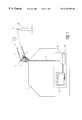
- FIG. 1shows the basic design of the user channel uplink or the downlink channel used by one embodiment of a satellite reception/transmission system according to the invention
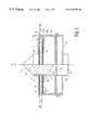
- FIG. 2shows a vertical section through the line A—A of FIG. 3. a of one embodiment of a device according to the invention
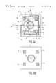
- FIG. 3. ashows a top view through line B—B of FIG. 2 of one embodiment of the reception circuit board according to the invention
- FIG. 3. bshows a bottom view through the line C—C of FIG. 2 of one embodiment of the auxiliary circuit board according to the invention
- FIG. 3. cshows an enlarged view of a region D of FIG. 2,
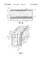
- FIG. 4shows a perspective view of a variant of the invention
- FIG. 5shows a variant of the embodiment of FIG. 2 .
- FIG. 1shows the basic design of the downlink channel used by a satellite reception/transmission system according to the invention.
- information distributed by the reception/transmission systemmay in particular originate from satellites, from recording studios, from hardwired networks, or may be exchanged within the framework of an MMDS (Multipoint Multichannel Distribution System), LMDS (Local Multipoint Distribution System) or MVDS (Multipoint Video Distribution System) system well known to those skilled in the art.
- MMDSMultipoint Multichannel Distribution System
- LMDSLocal Multipoint Distribution System
- MVDSMultipoint Video Distribution System
- the envisaged frameworkis that of a bidirectional satellite-user-satellite link.
- a satellite 1sends information items and programmes 2 available to users. These information items and programmes 2 are picked up by each user via the reception/transmission system having a small-diameter antenna 3 placed on the roof of a house 4 for example.
- the antenna 3has a reflector 5 designed to focus the received energy onto its focus close to which a primary source 6 is housed, which source picks up and radiates the energy thus exchanged, having a frequency conversion device which is not shown for reasons of clarity.
- This converterconverts the signals received by the satellite into intermediate frequencies and transmits them, via link means, for example a coaxial cable 8 , to an interior unit 9 placed inside a house 4 , comprising a decoder/coder 10 linked to means for using the transmitted information, for example a television receiver 11 .
- this antenna 3because of its small size, can be placed near the balcony of one storey.
- a reception/transmitting antennacan be located at the top of the multistorey building and can be fitted with a first converter for conversion to higher frequencies (frequency bands close to 40 GHz) for cordless distribution of the signals to the various storeys.
- the antenna 3then plays the role of collecting the signals thus distributed and a second frequency converter has the function of converting them to intermediate frequencies.
- the said antenna 3is also used for the downlink 12 or the uplink 12 .
- the userby means of a remote control for example, can reply to an interactive service.
- Information itemsare coded then transmitted, by means of the cable 8 , to the high-frequency converter which converts the said information items into a higher transmission frequency band.
- the “user” uplink 12transmits return data to the satellite 1 which therefore plays the role, among others, of collector and centralizer of the data transmitted by users for retransmission with a view to subsequent processing.
- the embodiment thus describedtherefore demonstrates a reception/transmission system in which the primary source 6 points in the same direction for transmission and reception.
- the reception/transmission systemhas to comprise a primary source 6 whose receiving antenna and transmitting antenna are such that their respective radiation patterns are maximized in one and the same direction.
- the information items 2could for example come from the satellite 1 and the return data could be transmitted to the MMDS earth station 13 .
- This downlinkis shown in dotted lines on FIG. 2 .
- the system according to the inventionhas to comprise one receiving antenna and one transmitting antenna pointing in two different directions, which means that at least one of the two antennas has to be out of focus.
- the uplink 12operates in the 6.4 GHz to 6.7 GHz frequency band
- the downlink 2denoting the channel for receiving, via the antenna 3 the information transmitted by the satellite 1 , operates in the 3.7 GHz to 4.2 GHz frequency band.
- the extended band Cwhose downlink 2 operates at the 3.4 GHz to 4.2 GHz frequency band, can also be used.
- Data transmitted on the uplink 12can be data relating to pay television, or more generally interactive television which provides the user with access to films, interactive games, telepurchasing and the downloading of software but also to services such as database consultation, reservations, etc.
- FIG. 2shows a vertical section through the line A—A of FIG. 3. a of one embodiment of a device 15 according to the invention in which a reception circuit board 16 , a transmission circuit board 27 and an auxiliary circuit board 17 are provided.
- FIG. 3. ashows a top view through the line B—B of FIG. 2 of an embodiment of the reception circuit board 16 according to the invention while FIG. 3. b shows a bottom view through the line C—C of FIG. 2 of an embodiment of the auxiliary circuit board 17 , FIG. 3. c showing an enlarged view of a region D of FIG. 2 which reveals the detailed structure of the various components of the reception circuit board 16 and of the auxiliary circuit board 17 .
- FIG. 4shows a perspective view of a variant of the embodiment of the invention described in FIGS. 2 and 3 . a to 3 . c.
- the device 15has a parallelepipedal support or body 18 made of a conducting material, and a rod 19 .
- the rod 19has a cone 20 coming out of the top face 21 of the said body 18 , whose circular base is centred on the intersection of the diagonals of the said top rectangular face 21 and whose vertex points out into space into which waves are radiated or from which waves are picked up.
- the base of this cone 20is extended into a cylinder 22 and terminates in a cone 23 whose vertex points in the opposite direction to that of the cone 20 .
- the rod 19 formed by the cone 20 , the cylinder 22 and the cone 23is made for example of compressed polystyrene, forming a longitudinal radiation dielectric antenna, namely one having a relatively narrow, rodlike, radiation pattern.
- the shape of this rod 19explains to its name of cylindro-conical antenna.
- the rod 19functions as a waveguide and transmits in a mode such that the radiation maximum appears along the direction of the rod 19 .
- the rod 19is hollow.
- the technology of such dielectric antennasis explained for example in the book “Techniques de l' registration—Traotti Electronique [Techniques for the Engineer—Electronic Treatise]”, E3 283—p.11, version 3-1991.
- the rod 19is surrounded, below the base of the cone 20 in the direction of wave reception, by a cylindrical shell 24 whose axis D is coincident with axis of the rod 19 .
- This shell 24has, in the example, an external diameter of 3.66 cm and an internal diameter of 3.25 cm.
- the shell 24extends inside the body 18 perpendicular to the cross sections of the latter and ends in a part which emerges from the lower face 25 of the body 18 .
- This shell 24which is made of conducting material, forms a waveguide whose walls are in contact with the body 18 .
- the end part of the shell 24 emerging from the upper face 21is open while that emerging from the lower face 25 of the shell 24 is closed by a metal plate 26 .
- the shell 24 with its bottom 26forms a resonant cavity.
- the shell 24is split perpendicularly into two parts 24 1 and 24 2 between which the transmission circuit board 27 of the electromagnetic wave transmission microstrip circuit is placed, into a straight section of the shell 24 .
- the combination formed by the shell 24 and the rod 19will be called a guide.
- the circuit board 27which forms a substrate, is made from a material of given dielectric permitivity, for example Teflon glass. It has an upper surface 27 1 , turned towards the rod 19 and a lower surface 27 2 located on the other face of the substrate. The lower surface 27 2 is metallized, forming an earth plane, and is in contact with the conducting walls of the shell 24 .
- the circuit board 27is fed by two coplanar probes 280 1 , and 280 2 which etched into the upper surface 27 1 , and which penetrate inside the shell 24 through apertures without touching the wall of the shell 24 . To enable the transmission of orthogonally polarized waves, the two probes 280 1 , and 280 2 are arranged at right angles to each other.
- This transmission circuitwhich in the present embodiment is arranged on the circuit board 27 , comprises a power amplifier and a frequency converter connected to the interior unit 9 via the coaxial cable 8 .
- the devicealso has a radiator 36 located behind the transmission circuit board 27 of the microstrip transmission circuit, the said radiator being designed to dissipate the heat released by a power amplifier (not shown) laid out in the transmission circuit on the board 27 .
- a power amplifiernot shown
- the part 24 2 closing the shell 24is a section of quarter-wave waveguide of length ⁇ GT /4 (length of the guided wave) forming a resonant cavity and functioning as an open circuit in the plane of the circuit board 27 for transmitted: waves, ⁇ GT being the wavelength of the-guided wave transmitted.
- the upper face 21has a substrate 28 followed successively in the wave reception direction, by an array of radiating elements 29 1 , 29 2 , 29 3 , 29 4 for receiving electromagnetic waves, then by a space filled with foam to a thickness of between, for example, 4 mm to 7 mm, then an array of radiating elements 30 1 , 30 2 , 30 3 , 30 4 for receiving electromagnetic waves, the array being associated with a microstrip excitation circuit 31 , these being etched in a substrate 320 .
- the radiating elements of the substrate 28are formed by four square flat patches 29 1 , 29 2 , 29 3 , 29 4 , etched in the lower face 28 1 , of the substrate 28 turned towards the inside of the body 18 and arranged uniformly around the centre of the substrate 28 .
- the radiating elements of the circuit board 26are formed by four square flat patches 30 1 , 30 2 , 30 3 , 30 4 , etched in the upper face of substrate 320 of the circuit board 16 , each patch 30 1 to 30 4 being arranged respectively opposite the corresponding patch 29 1 to 29 4 .
- the lower surface 320 1 of the substrate 320 turned towards the cavity 24 2is metallized, forming an earth plane, and is in contact with the conducting walls of the shell 24 while the upper surface turned towards the cone 20 has the patches 30 1 , 30 2 , 30 3 , 30 4 and the excitation circuit 31 .
- FIG. 3. ashows the various elements forming the reception circuit board 16 .
- This circuit boardhas a circular aperture whose centre is coincident with that of the circuit board 16 through which the shell 24 passes and round which the four patches 30 1 , 30 2 , 30 3 , 30 4 are arranged.
- the circuit board 16also has the excitation circuit 31 comprising lines 32 designed to carry vertically polarized waves and lines 33 designed to conduct horizontally polarized waves.
- quadrants 34 1 , 34 2 , 34 3 , 34 4can be defined, these being bounded by the horizontal 35 1 and vertical 35 2 mid-lines of the circuit board 16 passing respectively through the middle of the vertical and horizontal edges of the circuit board 16 .
- These quadrants 34 1 , 34 2 , 34 3 , 34 4have respectively the patches 30 1 , 30 2 , 30 3 , 30 4 , each patch being arranged symmetrically with the patch contained in the bordering quadrant with respect to the horizontal 35 1 and vertical 35 2 mid-lines.
- Each patch 30 1 , 30 2has, respectively, a point of connection A 1 , A 2 between the upper edge of the said patch 30 1 , 30 2 and respectively a vertical excitation line L 1 , L 2 designed to guide vertically polarized waves. These two lines L 1 , L 2 both bend at right angles and join together an intersection point C 1 situated on the vertical mid-line 35 2 .
- each patch 30 3 and 30 4has, respectively, a connection point A 3 , A 4 between the lower edge of the said patch 30 3 , 30 4 with respectively a vertical excitation line L 3 , L 4 designed to guide vertically polarized waves.
- These two lines L 3 , L 4are both bent at right angles and join together at a connection point C 2 situated on the vertical mid-line 35 2 .
- patches 30 1 , 30 3have respectively a connection point B 1 , B 3 between both the right edge of the patches 30 1 , 30 3 respectively and the horizontal excitation line L 5 , L 6 respectively designed to guide horizontally polarized waves.
- the patches 30 2 , 30 4have respectively an intersection point B 2 , B 4 between the left edge of the said patches 30 2 , 30 4 and a horizontal excitation line L 7 , L 8 designed to guide horizontally polarized waves.
- the lines L 5 and L 7meet at a point C 5 contained in the quadrant 34 1 and at a distance ⁇ L from the mid-line 35 2 while the lines L 6 and L 8 meet at a point C 6 contained in the quadrant 34 3 and also separated by distance ⁇ L from the mid-line 35 2 , so that the said points C 5 and C 6 are symmetrical with respect to the mid-line 35 1 . From these points C 5 and C 6 start two lines which meet at a point C 7 located on the mid-line 35 1 from which starts a principal excitation line which is designed to guide horizontally polarized waves and ends at a connection point C 8 .
- the upper face 21is square with sides of length 10 cm and the body has a height of approximately 8 cm.
- the shell 24has an internal diameter of 3.25 cm and an external diameter of 3.66 cm.
- the patches 29 1 , 29 2 , 29 3 , 29 4 , 30 1 , 30 2 , 30 3 , 30 4have respectively one side approximately equal to ⁇ GR /2, ⁇ GR being the wavelength of the guided wave received. Furthermore, it is possible to use a substrate based on ceramic-filled Teflon.
- FIG. 3. bshows the various components of the auxiliary circuit board 17 .
- This circuit boardhas four patches 29 1 , 29 2 , 29 3 , 29 4 and a circular aperture centred on the centre of the circuit board 17 through which the shell 24 passes.
- FIG. 3. cshows an enlarged view of the region D of FIG. 2, revealing a detailed picture of the various components of the two circuit boards 16 and 17 .
- the thickness ⁇ of foammay, in the present embodiment, be around 0.06 to 0.08 times the wavelength ⁇ GR of the received wave, i.e. around 4 mm to 7 mm.
- the device according to the present embodimenthas an intermediate circuit board 37 on which the reception circuit (not shown) comprising at least one low-noise amplifier and a frequency converter are laid out.
- Coaxial cables(for reasons of clarity, only one coaxial cable 38 has been drawn) connect the connection points C 4 and C 8 to the reception circuit of the circuit board 37 with a view to processing the signals received.
- the output of the reception circuitis connected, through an aperture 39 made in the body 18 , to the coaxial cable 8 .
- a single oscillatorcan be used for the conversion to high frequencies of the signals that are to be transmitted and for the conversion to low frequencies of the signals that are to be received. More generally, several identical components may be used for the conversion of received and transmitted signals.
- the circuit board 37can act as a support for these different components. Within this framework, at least one coaxial cable is laid out between the circuit board 37 and the transmission circuit board 27 .
- FIG. 5shows an important variation of the embodiment of FIG. 2 .
- the rod 19is advantageously replaced with a coaxial line 42 , one end of which is connected to the transmission circuits and the other end of which is connected to a helix 40 made up of a series of turns 41 , this helical antenna operating in axial mode.
- the circular cross section of the helixis then reduced to one-third of the wavelength.
- the diameter of the shell 24undergoes a discontinuity at the link between the coaxial line and the helix.
- the device according to the inventionoperates as follows:
- Electromagnetic waves arriving at the reflector 5are reflected and focused onto the reflector focus which is located near the geometric centre of the array of the circuit board 17 .
- the array of the circuit board 16operates at a central resonant frequency F 0 while the array of the circuit board 17 operates as a resonant frequency F 0 ′ which is slightly offset with respect to the said frequency F 0 , so that the combination of the two circuit boards 16 and 17 acts as a single array with an extended bandwidth.
- the patches 30 1 , 30 2 , 30 3 , 30 4are all fed in phase and with the same amplitude by two microstrip power dividers, the patch feed having to be in phase so that the electric fields are additive in the propagation direction of the guided waves.
- B 1 , B 2 and B 3 , B 4are excited by opposite sides of the patches, respectively.
- the patch 30 1is excited by its right side, which creates, at time t, a field E oriented from right to left
- the patch 30 2is excited by its left side, which creates, at the same time t, a field E oriented from left to right, which finally creates fields which are out of phase by ⁇ .
- This configurationimproves the quality of the polarization since it eliminates the problems of cross polarization. Furthermore, because of the symmetries existing between the patches which are side by side, the reflections of the waves are cancelled out.
- the said waves, received and carried by the lines 32 and 33are delivered, via the cable 38 , to the reception circuit of the circuit board 37 , for example, which, after conversion of the received signals into intermediate frequencies, transmits these signals to the interior unit 9 via the cable 8 .
- the signals coming from the said unit 9pass through the frequency conversion circuit, laid out on the circuit board 27 for example, and supply the probes 280 1 , 280 2 with waves to be transmitted to the rod 19 which transmits the maximum power along the axis D of the rod 19 .
- the cylindro-conical shape of the guide ( 19 , 24 ) upstream of the first circuit board ( 16 ) in the wave reception directionmeans that the radiation pattern of the said array of radiating elements ( 30 1 , 30 2 , 30 3 , 30 4 ) is not disturbed.
- the device according to the inventionmeans that a single device can operate simultaneously and in a completely decoupled manner, as a reception channel and a transmission channel.
- the guide ( 19 , 24 ) and the array of radiating elements ( 30 1 , 30 2 , 30 3 , 30 4 )are laid out so that their respective phase centres are nearly coincident at a single point forming the phase centre of the said device, allowing the said device to operate, in reception and in transmission, as a primary source pointing in a given direction, this primary source being located at the focus of the focusing means of a reception/transmission system according to the invention, such as a parabola or an electromagnetic lens.
- At least one of the phase centrescan be defocused so as to transmit in a direction other than the reception direction.
- the devices according to the inventioncan also be implemented in the clusters of satellites in circular orbits, particularly in low orbit (Low Earth Orbit or LEO) or in mid orbit (Mid Earth Orbit or MEO).
- LEOLow Earth Orbit
- MEOMid orbit
- the device according to the inventionenables a ratio between the central frequencies of the transmission and reception bands respectively of less than or equal to three to be obtained, with a small number of patches such as 4, in order to minimize the complexity of the device.
- the device of the prior art cited in the preamble of the present applicationdoes not allow reception and transmission in the frequency bands Fb and Fh respectively for reception and transmission to be close enough if any four radiating elements are considered. So, if d 1 is the distance separating two radiating elements which are symmetrically opposed with respect to the phase centre, and d 2 is the diameter of the horn, and Lb and Lh are the wavelengths corresponding to the frequencies Fb and Fh respectively, in order to obtain the equivalent illumination at the two frequencies it is typically necessary to have:
- the path difference ⁇ Lcan be zero.
- reception and transmission circuits of the device according to the inventioncan also be arranged on one and the same circuit board having the double function of supporting the reception circuit and the transmission circuit.
- said circuitsare laid out in such a way as to avoid any electromagnetic coupling between the reception circuit and the transmission circuit.
- junctions between the excitation lines of the reception circuit and those of transmission circuitwould be provided, for example, by bridges.
Landscapes
- Physics & Mathematics (AREA)
- Electromagnetism (AREA)
- Variable-Direction Aerials And Aerial Arrays (AREA)
- Waveguide Aerials (AREA)
Abstract
Description
Claims (14)
Applications Claiming Priority (3)
| Application Number | Priority Date | Filing Date | Title |
|---|---|---|---|
| FR9716767 | 1997-12-31 | ||
| FR9716767AFR2773271B1 (en) | 1997-12-31 | 1997-12-31 | ELECTROMAGNETIC WAVE TRANSMITTER / RECEIVER |
| PCT/FR1998/002922WO1999035711A1 (en) | 1997-12-31 | 1998-12-30 | Electromagnetic wave transmitter/receiver |
Publications (1)
| Publication Number | Publication Date |
|---|---|
| US6362788B1true US6362788B1 (en) | 2002-03-26 |
Family
ID=9515354
Family Applications (1)
| Application Number | Title | Priority Date | Filing Date |
|---|---|---|---|
| US09/582,395Expired - LifetimeUS6362788B1 (en) | 1997-12-31 | 1998-12-30 | Electromagnetic wave transmitter/receiver |
Country Status (8)
| Country | Link |
|---|---|
| US (1) | US6362788B1 (en) |
| EP (1) | EP1044482A1 (en) |
| JP (1) | JP2002501315A (en) |
| KR (1) | KR100592422B1 (en) |
| CN (1) | CN1114244C (en) |
| FR (1) | FR2773271B1 (en) |
| ID (1) | ID27106A (en) |
| WO (1) | WO1999035711A1 (en) |
Cited By (141)
| Publication number | Priority date | Publication date | Assignee | Title |
|---|---|---|---|---|
| US6535169B2 (en)* | 2000-06-09 | 2003-03-18 | Thomson Licensing S.A. | Source antennas for transmitting/receiving electromagnetic waves for satellite telecommunications systems |
| US20060028386A1 (en)* | 1999-11-18 | 2006-02-09 | Ebling James P | Multi-beam antenna |
| EP1517403A3 (en)* | 2003-08-29 | 2006-04-12 | Fujitsu Ten Limited | Circular polarization antenna and composite antenna including this antenna |
| US20060189273A1 (en)* | 2005-02-18 | 2006-08-24 | U.S. Monolithics, L.L.C. | Systems, methods and devices for a ku/ka band transmitter-receiver |
| US20060267830A1 (en)* | 2005-02-10 | 2006-11-30 | O'boyle Michael E | Automotive radar system with guard beam |
| US20070001918A1 (en)* | 2005-05-05 | 2007-01-04 | Ebling James P | Antenna |
| WO2007060148A1 (en)* | 2005-11-24 | 2007-05-31 | Thomson Licensing | Antenna arrays with dual circular polarization |
| US20070195004A1 (en)* | 1999-11-18 | 2007-08-23 | Gabriel Rebeiz | Multi-beam antenna |
| US20080090516A1 (en)* | 2004-10-21 | 2008-04-17 | Eads Astrium Limited | System For Processing Radio Frequency Signals |
| KR101000354B1 (en) | 2008-04-15 | 2010-12-13 | 주식회사 에이스테크놀로지 | Window-mounted antenna with front and rear defense characteristics |
| US9630227B2 (en) | 2010-05-06 | 2017-04-25 | Primetals Technologies Germany Gmbh | Operating method for a production line with prediction of the command speed |
| US9667317B2 (en) | 2015-06-15 | 2017-05-30 | At&T Intellectual Property I, L.P. | Method and apparatus for providing security using network traffic adjustments |
| US9674711B2 (en) | 2013-11-06 | 2017-06-06 | At&T Intellectual Property I, L.P. | Surface-wave communications and methods thereof |
| US9685992B2 (en) | 2014-10-03 | 2017-06-20 | At&T Intellectual Property I, L.P. | Circuit panel network and methods thereof |
| US9705610B2 (en) | 2014-10-21 | 2017-07-11 | At&T Intellectual Property I, L.P. | Transmission device with impairment compensation and methods for use therewith |
| US9705561B2 (en) | 2015-04-24 | 2017-07-11 | At&T Intellectual Property I, L.P. | Directional coupling device and methods for use therewith |
| US9722318B2 (en) | 2015-07-14 | 2017-08-01 | At&T Intellectual Property I, L.P. | Method and apparatus for coupling an antenna to a device |
| US9729197B2 (en) | 2015-10-01 | 2017-08-08 | At&T Intellectual Property I, L.P. | Method and apparatus for communicating network management traffic over a network |
| US9735833B2 (en) | 2015-07-31 | 2017-08-15 | At&T Intellectual Property I, L.P. | Method and apparatus for communications management in a neighborhood network |
| US9742521B2 (en) | 2014-11-20 | 2017-08-22 | At&T Intellectual Property I, L.P. | Transmission device with mode division multiplexing and methods for use therewith |
| US9742462B2 (en) | 2014-12-04 | 2017-08-22 | At&T Intellectual Property I, L.P. | Transmission medium and communication interfaces and methods for use therewith |
| US9749013B2 (en) | 2015-03-17 | 2017-08-29 | At&T Intellectual Property I, L.P. | Method and apparatus for reducing attenuation of electromagnetic waves guided by a transmission medium |
| US9749053B2 (en) | 2015-07-23 | 2017-08-29 | At&T Intellectual Property I, L.P. | Node device, repeater and methods for use therewith |
| US9748626B2 (en) | 2015-05-14 | 2017-08-29 | At&T Intellectual Property I, L.P. | Plurality of cables having different cross-sectional shapes which are bundled together to form a transmission medium |
| US9768833B2 (en) | 2014-09-15 | 2017-09-19 | At&T Intellectual Property I, L.P. | Method and apparatus for sensing a condition in a transmission medium of electromagnetic waves |
| US9769020B2 (en) | 2014-10-21 | 2017-09-19 | At&T Intellectual Property I, L.P. | Method and apparatus for responding to events affecting communications in a communication network |
| US9769128B2 (en) | 2015-09-28 | 2017-09-19 | At&T Intellectual Property I, L.P. | Method and apparatus for encryption of communications over a network |
| US9780834B2 (en) | 2014-10-21 | 2017-10-03 | At&T Intellectual Property I, L.P. | Method and apparatus for transmitting electromagnetic waves |
| US9787412B2 (en) | 2015-06-25 | 2017-10-10 | At&T Intellectual Property I, L.P. | Methods and apparatus for inducing a fundamental wave mode on a transmission medium |
| US9793955B2 (en) | 2015-04-24 | 2017-10-17 | At&T Intellectual Property I, Lp | Passive electrical coupling device and methods for use therewith |
| US9793951B2 (en) | 2015-07-15 | 2017-10-17 | At&T Intellectual Property I, L.P. | Method and apparatus for launching a wave mode that mitigates interference |
| US9793954B2 (en) | 2015-04-28 | 2017-10-17 | At&T Intellectual Property I, L.P. | Magnetic coupling device and methods for use therewith |
| US9800327B2 (en) | 2014-11-20 | 2017-10-24 | At&T Intellectual Property I, L.P. | Apparatus for controlling operations of a communication device and methods thereof |
| US9820146B2 (en) | 2015-06-12 | 2017-11-14 | At&T Intellectual Property I, L.P. | Method and apparatus for authentication and identity management of communicating devices |
| US9838896B1 (en) | 2016-12-09 | 2017-12-05 | At&T Intellectual Property I, L.P. | Method and apparatus for assessing network coverage |
| US9838078B2 (en) | 2015-07-31 | 2017-12-05 | At&T Intellectual Property I, L.P. | Method and apparatus for exchanging communication signals |
| US9847850B2 (en) | 2014-10-14 | 2017-12-19 | At&T Intellectual Property I, L.P. | Method and apparatus for adjusting a mode of communication in a communication network |
| US9847566B2 (en) | 2015-07-14 | 2017-12-19 | At&T Intellectual Property I, L.P. | Method and apparatus for adjusting a field of a signal to mitigate interference |
| US9853342B2 (en) | 2015-07-14 | 2017-12-26 | At&T Intellectual Property I, L.P. | Dielectric transmission medium connector and methods for use therewith |
| US9860075B1 (en) | 2016-08-26 | 2018-01-02 | At&T Intellectual Property I, L.P. | Method and communication node for broadband distribution |
| US9866309B2 (en) | 2015-06-03 | 2018-01-09 | At&T Intellectual Property I, Lp | Host node device and methods for use therewith |
| US9865911B2 (en) | 2015-06-25 | 2018-01-09 | At&T Intellectual Property I, L.P. | Waveguide system for slot radiating first electromagnetic waves that are combined into a non-fundamental wave mode second electromagnetic wave on a transmission medium |
| US9866276B2 (en) | 2014-10-10 | 2018-01-09 | At&T Intellectual Property I, L.P. | Method and apparatus for arranging communication sessions in a communication system |
| US9871558B2 (en) | 2014-10-21 | 2018-01-16 | At&T Intellectual Property I, L.P. | Guided-wave transmission device and methods for use therewith |
| US9871282B2 (en) | 2015-05-14 | 2018-01-16 | At&T Intellectual Property I, L.P. | At least one transmission medium having a dielectric surface that is covered at least in part by a second dielectric |
| US9871283B2 (en) | 2015-07-23 | 2018-01-16 | At&T Intellectual Property I, Lp | Transmission medium having a dielectric core comprised of plural members connected by a ball and socket configuration |
| US9876571B2 (en) | 2015-02-20 | 2018-01-23 | At&T Intellectual Property I, Lp | Guided-wave transmission device with non-fundamental mode propagation and methods for use therewith |
| US9876264B2 (en) | 2015-10-02 | 2018-01-23 | At&T Intellectual Property I, Lp | Communication system, guided wave switch and methods for use therewith |
| US9876605B1 (en) | 2016-10-21 | 2018-01-23 | At&T Intellectual Property I, L.P. | Launcher and coupling system to support desired guided wave mode |
| US9882257B2 (en) | 2015-07-14 | 2018-01-30 | At&T Intellectual Property I, L.P. | Method and apparatus for launching a wave mode that mitigates interference |
| US9887447B2 (en) | 2015-05-14 | 2018-02-06 | At&T Intellectual Property I, L.P. | Transmission medium having multiple cores and methods for use therewith |
| US9893795B1 (en) | 2016-12-07 | 2018-02-13 | At&T Intellectual Property I, Lp | Method and repeater for broadband distribution |
| US9904535B2 (en) | 2015-09-14 | 2018-02-27 | At&T Intellectual Property I, L.P. | Method and apparatus for distributing software |
| US9906269B2 (en) | 2014-09-17 | 2018-02-27 | At&T Intellectual Property I, L.P. | Monitoring and mitigating conditions in a communication network |
| US9912033B2 (en) | 2014-10-21 | 2018-03-06 | At&T Intellectual Property I, Lp | Guided wave coupler, coupling module and methods for use therewith |
| US9912027B2 (en) | 2015-07-23 | 2018-03-06 | At&T Intellectual Property I, L.P. | Method and apparatus for exchanging communication signals |
| US9911020B1 (en) | 2016-12-08 | 2018-03-06 | At&T Intellectual Property I, L.P. | Method and apparatus for tracking via a radio frequency identification device |
| US9913139B2 (en) | 2015-06-09 | 2018-03-06 | At&T Intellectual Property I, L.P. | Signal fingerprinting for authentication of communicating devices |
| US9912381B2 (en) | 2015-06-03 | 2018-03-06 | At&T Intellectual Property I, Lp | Network termination and methods for use therewith |
| US9917341B2 (en) | 2015-05-27 | 2018-03-13 | At&T Intellectual Property I, L.P. | Apparatus and method for launching electromagnetic waves and for modifying radial dimensions of the propagating electromagnetic waves |
| US9927517B1 (en) | 2016-12-06 | 2018-03-27 | At&T Intellectual Property I, L.P. | Apparatus and methods for sensing rainfall |
| US9929755B2 (en) | 2015-07-14 | 2018-03-27 | At&T Intellectual Property I, L.P. | Method and apparatus for coupling an antenna to a device |
| US9948333B2 (en) | 2015-07-23 | 2018-04-17 | At&T Intellectual Property I, L.P. | Method and apparatus for wireless communications to mitigate interference |
| US9954286B2 (en) | 2014-10-21 | 2018-04-24 | At&T Intellectual Property I, L.P. | Guided-wave transmission device with non-fundamental mode propagation and methods for use therewith |
| US9954287B2 (en) | 2014-11-20 | 2018-04-24 | At&T Intellectual Property I, L.P. | Apparatus for converting wireless signals and electromagnetic waves and methods thereof |
| US9967173B2 (en) | 2015-07-31 | 2018-05-08 | At&T Intellectual Property I, L.P. | Method and apparatus for authentication and identity management of communicating devices |
| US9973416B2 (en) | 2014-10-02 | 2018-05-15 | At&T Intellectual Property I, L.P. | Method and apparatus that provides fault tolerance in a communication network |
| US9973940B1 (en) | 2017-02-27 | 2018-05-15 | At&T Intellectual Property I, L.P. | Apparatus and methods for dynamic impedance matching of a guided wave launcher |
| US9991580B2 (en) | 2016-10-21 | 2018-06-05 | At&T Intellectual Property I, L.P. | Launcher and coupling system for guided wave mode cancellation |
| US9998870B1 (en) | 2016-12-08 | 2018-06-12 | At&T Intellectual Property I, L.P. | Method and apparatus for proximity sensing |
| US9999038B2 (en) | 2013-05-31 | 2018-06-12 | At&T Intellectual Property I, L.P. | Remote distributed antenna system |
| US9997819B2 (en) | 2015-06-09 | 2018-06-12 | At&T Intellectual Property I, L.P. | Transmission medium and method for facilitating propagation of electromagnetic waves via a core |
| US10009067B2 (en) | 2014-12-04 | 2018-06-26 | At&T Intellectual Property I, L.P. | Method and apparatus for configuring a communication interface |
| US10020844B2 (en) | 2016-12-06 | 2018-07-10 | T&T Intellectual Property I, L.P. | Method and apparatus for broadcast communication via guided waves |
| US10027397B2 (en) | 2016-12-07 | 2018-07-17 | At&T Intellectual Property I, L.P. | Distributed antenna system and methods for use therewith |
| US10033107B2 (en) | 2015-07-14 | 2018-07-24 | At&T Intellectual Property I, L.P. | Method and apparatus for coupling an antenna to a device |
| US10033108B2 (en) | 2015-07-14 | 2018-07-24 | At&T Intellectual Property I, L.P. | Apparatus and methods for generating an electromagnetic wave having a wave mode that mitigates interference |
| US10044409B2 (en) | 2015-07-14 | 2018-08-07 | At&T Intellectual Property I, L.P. | Transmission medium and methods for use therewith |
| US10051630B2 (en) | 2013-05-31 | 2018-08-14 | At&T Intellectual Property I, L.P. | Remote distributed antenna system |
| US10069185B2 (en) | 2015-06-25 | 2018-09-04 | At&T Intellectual Property I, L.P. | Methods and apparatus for inducing a non-fundamental wave mode on a transmission medium |
| US10069535B2 (en) | 2016-12-08 | 2018-09-04 | At&T Intellectual Property I, L.P. | Apparatus and methods for launching electromagnetic waves having a certain electric field structure |
| US10090606B2 (en) | 2015-07-15 | 2018-10-02 | At&T Intellectual Property I, L.P. | Antenna system with dielectric array and methods for use therewith |
| US10090594B2 (en) | 2016-11-23 | 2018-10-02 | At&T Intellectual Property I, L.P. | Antenna system having structural configurations for assembly |
| US10103422B2 (en) | 2016-12-08 | 2018-10-16 | At&T Intellectual Property I, L.P. | Method and apparatus for mounting network devices |
| US10129057B2 (en) | 2015-07-14 | 2018-11-13 | At&T Intellectual Property I, L.P. | Apparatus and methods for inducing electromagnetic waves on a cable |
| US10135145B2 (en) | 2016-12-06 | 2018-11-20 | At&T Intellectual Property I, L.P. | Apparatus and methods for generating an electromagnetic wave along a transmission medium |
| US10135147B2 (en) | 2016-10-18 | 2018-11-20 | At&T Intellectual Property I, L.P. | Apparatus and methods for launching guided waves via an antenna |
| US10135146B2 (en) | 2016-10-18 | 2018-11-20 | At&T Intellectual Property I, L.P. | Apparatus and methods for launching guided waves via circuits |
| US10139820B2 (en) | 2016-12-07 | 2018-11-27 | At&T Intellectual Property I, L.P. | Method and apparatus for deploying equipment of a communication system |
| US10148016B2 (en) | 2015-07-14 | 2018-12-04 | At&T Intellectual Property I, L.P. | Apparatus and methods for communicating utilizing an antenna array |
| US10170840B2 (en) | 2015-07-14 | 2019-01-01 | At&T Intellectual Property I, L.P. | Apparatus and methods for sending or receiving electromagnetic signals |
| US10168695B2 (en) | 2016-12-07 | 2019-01-01 | At&T Intellectual Property I, L.P. | Method and apparatus for controlling an unmanned aircraft |
| US10178445B2 (en) | 2016-11-23 | 2019-01-08 | At&T Intellectual Property I, L.P. | Methods, devices, and systems for load balancing between a plurality of waveguides |
| US10205655B2 (en) | 2015-07-14 | 2019-02-12 | At&T Intellectual Property I, L.P. | Apparatus and methods for communicating utilizing an antenna array and multiple communication paths |
| US10225025B2 (en) | 2016-11-03 | 2019-03-05 | At&T Intellectual Property I, L.P. | Method and apparatus for detecting a fault in a communication system |
| US10224634B2 (en) | 2016-11-03 | 2019-03-05 | At&T Intellectual Property I, L.P. | Methods and apparatus for adjusting an operational characteristic of an antenna |
| US10243784B2 (en) | 2014-11-20 | 2019-03-26 | At&T Intellectual Property I, L.P. | System for generating topology information and methods thereof |
| US10243270B2 (en) | 2016-12-07 | 2019-03-26 | At&T Intellectual Property I, L.P. | Beam adaptive multi-feed dielectric antenna system and methods for use therewith |
| US10264586B2 (en) | 2016-12-09 | 2019-04-16 | At&T Mobility Ii Llc | Cloud-based packet controller and methods for use therewith |
| US10291334B2 (en) | 2016-11-03 | 2019-05-14 | At&T Intellectual Property I, L.P. | System for detecting a fault in a communication system |
| US10298293B2 (en) | 2017-03-13 | 2019-05-21 | At&T Intellectual Property I, L.P. | Apparatus of communication utilizing wireless network devices |
| US10305190B2 (en) | 2016-12-01 | 2019-05-28 | At&T Intellectual Property I, L.P. | Reflecting dielectric antenna system and methods for use therewith |
| US10312567B2 (en) | 2016-10-26 | 2019-06-04 | At&T Intellectual Property I, L.P. | Launcher with planar strip antenna and methods for use therewith |
| US10320586B2 (en) | 2015-07-14 | 2019-06-11 | At&T Intellectual Property I, L.P. | Apparatus and methods for generating non-interfering electromagnetic waves on an insulated transmission medium |
| US10326689B2 (en) | 2016-12-08 | 2019-06-18 | At&T Intellectual Property I, L.P. | Method and system for providing alternative communication paths |
| US10326494B2 (en) | 2016-12-06 | 2019-06-18 | At&T Intellectual Property I, L.P. | Apparatus for measurement de-embedding and methods for use therewith |
| US10340600B2 (en) | 2016-10-18 | 2019-07-02 | At&T Intellectual Property I, L.P. | Apparatus and methods for launching guided waves via plural waveguide systems |
| US10340983B2 (en) | 2016-12-09 | 2019-07-02 | At&T Intellectual Property I, L.P. | Method and apparatus for surveying remote sites via guided wave communications |
| US10340603B2 (en) | 2016-11-23 | 2019-07-02 | At&T Intellectual Property I, L.P. | Antenna system having shielded structural configurations for assembly |
| US10340573B2 (en) | 2016-10-26 | 2019-07-02 | At&T Intellectual Property I, L.P. | Launcher with cylindrical coupling device and methods for use therewith |
| US10340601B2 (en) | 2016-11-23 | 2019-07-02 | At&T Intellectual Property I, L.P. | Multi-antenna system and methods for use therewith |
| US10341142B2 (en) | 2015-07-14 | 2019-07-02 | At&T Intellectual Property I, L.P. | Apparatus and methods for generating non-interfering electromagnetic waves on an uninsulated conductor |
| US10355367B2 (en) | 2015-10-16 | 2019-07-16 | At&T Intellectual Property I, L.P. | Antenna structure for exchanging wireless signals |
| US10359749B2 (en) | 2016-12-07 | 2019-07-23 | At&T Intellectual Property I, L.P. | Method and apparatus for utilities management via guided wave communication |
| US10361489B2 (en) | 2016-12-01 | 2019-07-23 | At&T Intellectual Property I, L.P. | Dielectric dish antenna system and methods for use therewith |
| US10374316B2 (en) | 2016-10-21 | 2019-08-06 | At&T Intellectual Property I, L.P. | System and dielectric antenna with non-uniform dielectric |
| US10382976B2 (en) | 2016-12-06 | 2019-08-13 | At&T Intellectual Property I, L.P. | Method and apparatus for managing wireless communications based on communication paths and network device positions |
| US10389029B2 (en) | 2016-12-07 | 2019-08-20 | At&T Intellectual Property I, L.P. | Multi-feed dielectric antenna system with core selection and methods for use therewith |
| US10389037B2 (en) | 2016-12-08 | 2019-08-20 | At&T Intellectual Property I, L.P. | Apparatus and methods for selecting sections of an antenna array and use therewith |
| US10411356B2 (en) | 2016-12-08 | 2019-09-10 | At&T Intellectual Property I, L.P. | Apparatus and methods for selectively targeting communication devices with an antenna array |
| US10439290B2 (en) | 2015-07-14 | 2019-10-08 | At&T Intellectual Property I, L.P. | Apparatus and methods for wireless communications |
| US10439675B2 (en) | 2016-12-06 | 2019-10-08 | At&T Intellectual Property I, L.P. | Method and apparatus for repeating guided wave communication signals |
| US10446936B2 (en) | 2016-12-07 | 2019-10-15 | At&T Intellectual Property I, L.P. | Multi-feed dielectric antenna system and methods for use therewith |
| US10498044B2 (en) | 2016-11-03 | 2019-12-03 | At&T Intellectual Property I, L.P. | Apparatus for configuring a surface of an antenna |
| US10511346B2 (en) | 2015-07-14 | 2019-12-17 | At&T Intellectual Property I, L.P. | Apparatus and methods for inducing electromagnetic waves on an uninsulated conductor |
| US10530505B2 (en) | 2016-12-08 | 2020-01-07 | At&T Intellectual Property I, L.P. | Apparatus and methods for launching electromagnetic waves along a transmission medium |
| US10535928B2 (en) | 2016-11-23 | 2020-01-14 | At&T Intellectual Property I, L.P. | Antenna system and methods for use therewith |
| US10547348B2 (en) | 2016-12-07 | 2020-01-28 | At&T Intellectual Property I, L.P. | Method and apparatus for switching transmission mediums in a communication system |
| US10601494B2 (en) | 2016-12-08 | 2020-03-24 | At&T Intellectual Property I, L.P. | Dual-band communication device and method for use therewith |
| US10637149B2 (en) | 2016-12-06 | 2020-04-28 | At&T Intellectual Property I, L.P. | Injection molded dielectric antenna and methods for use therewith |
| US10650940B2 (en) | 2015-05-15 | 2020-05-12 | At&T Intellectual Property I, L.P. | Transmission medium having a conductive material and methods for use therewith |
| US10694379B2 (en) | 2016-12-06 | 2020-06-23 | At&T Intellectual Property I, L.P. | Waveguide system with device-based authentication and methods for use therewith |
| US10727599B2 (en) | 2016-12-06 | 2020-07-28 | At&T Intellectual Property I, L.P. | Launcher with slot antenna and methods for use therewith |
| US10755542B2 (en) | 2016-12-06 | 2020-08-25 | At&T Intellectual Property I, L.P. | Method and apparatus for surveillance via guided wave communication |
| US10777873B2 (en) | 2016-12-08 | 2020-09-15 | At&T Intellectual Property I, L.P. | Method and apparatus for mounting network devices |
| US10790593B2 (en) | 2015-07-14 | 2020-09-29 | At&T Intellectual Property I, L.P. | Method and apparatus including an antenna comprising a lens and a body coupled to a feedline having a structure that reduces reflections of electromagnetic waves |
| US10797781B2 (en) | 2015-06-03 | 2020-10-06 | At&T Intellectual Property I, L.P. | Client node device and methods for use therewith |
| US10811767B2 (en) | 2016-10-21 | 2020-10-20 | At&T Intellectual Property I, L.P. | System and dielectric antenna with convex dielectric radome |
| US10819035B2 (en) | 2016-12-06 | 2020-10-27 | At&T Intellectual Property I, L.P. | Launcher with helical antenna and methods for use therewith |
| US10916969B2 (en) | 2016-12-08 | 2021-02-09 | At&T Intellectual Property I, L.P. | Method and apparatus for providing power using an inductive coupling |
| US10938108B2 (en) | 2016-12-08 | 2021-03-02 | At&T Intellectual Property I, L.P. | Frequency selective multi-feed dielectric antenna system and methods for use therewith |
Families Citing this family (9)
| Publication number | Priority date | Publication date | Assignee | Title |
|---|---|---|---|---|
| FR2810163A1 (en)* | 2000-06-09 | 2001-12-14 | Thomson Multimedia Sa | IMPROVEMENT TO ELECTROMAGNETIC WAVE EMISSION / RECEPTION SOURCE ANTENNAS |
| DE10039772A1 (en)* | 2000-08-16 | 2002-03-07 | Bosch Gmbh Robert | combination antenna |
| FR2821489A1 (en)* | 2001-02-23 | 2002-08-30 | Sta Satellite Terminal Access | Dual band elliptic reflector satellite link antenna has combined patch and rod feed |
| US20060229627A1 (en) | 2004-10-29 | 2006-10-12 | Hunt Margaret M | Variable angle spinal surgery instrument |
| EP2120293A1 (en)* | 2008-05-16 | 2009-11-18 | Kildal Antenna Consulting AB | Improved broadband multi-dipole antenna with frequency-independent radiation characteristics |
| CN102636571B (en)* | 2012-04-28 | 2014-10-08 | 哈尔滨工业大学 | Measuring method of horizontal shear guided wavelength in steel plate and electromagnetic ultrasonic transducer using same |
| CN113261159B (en)* | 2019-04-04 | 2022-12-13 | 华为技术有限公司 | Composite artificial dielectric and multiband antenna feeders |
| CN112701451A (en)* | 2019-10-23 | 2021-04-23 | 苏州博海创业微系统有限公司 | Microstrip antenna designed based on radiation oscillator combined with multiple physical quantities |
| CN116291403A (en)* | 2021-12-20 | 2023-06-23 | 新疆中核天山铀业有限公司 | A downhole instrument for detecting spatial distribution of infiltration seepage flow field |
Citations (3)
| Publication number | Priority date | Publication date | Assignee | Title |
|---|---|---|---|---|
| DE2603055A1 (en) | 1976-01-28 | 1977-08-04 | Rohde & Schwarz | Reflector antenna excitation system - comprises two mechanically coupled units each consisting of dipole and auxiliary reflector |
| US4825221A (en) | 1985-01-16 | 1989-04-25 | Junkosha Co., Ltd. | Directly emitting dielectric transmission line |
| US5041840A (en) | 1987-04-13 | 1991-08-20 | Frank Cipolla | Multiple frequency antenna feed |
Family Cites Families (4)
| Publication number | Priority date | Publication date | Assignee | Title |
|---|---|---|---|---|
| US3803617A (en)* | 1972-04-14 | 1974-04-09 | Nasa | High efficiency multifrequency feed |
| FR2465328A1 (en)* | 1979-09-07 | 1981-03-20 | Thomson Csf | AIR FOR PRIMARY RADAR AND SECONDARY RADAR |
| JPS6018004A (en)* | 1983-07-11 | 1985-01-30 | Nippon Telegr & Teleph Corp <Ntt> | Frequency sharing antenna |
| US5005019A (en)* | 1986-11-13 | 1991-04-02 | Communications Satellite Corporation | Electromagnetically coupled printed-circuit antennas having patches or slots capacitively coupled to feedlines |
- 1997
- 1997-12-31FRFR9716767Apatent/FR2773271B1/ennot_activeExpired - Fee Related
- 1998
- 1998-12-30WOPCT/FR1998/002922patent/WO1999035711A1/ennot_activeApplication Discontinuation
- 1998-12-30JPJP2000527992Apatent/JP2002501315A/enactivePending
- 1998-12-30KRKR1020007007171Apatent/KR100592422B1/ennot_activeExpired - Fee Related
- 1998-12-30USUS09/582,395patent/US6362788B1/ennot_activeExpired - Lifetime
- 1998-12-30EPEP98964558Apatent/EP1044482A1/ennot_activeCeased
- 1998-12-30IDIDW20001285Apatent/ID27106A/enunknown
- 1998-12-30CNCN98812824Apatent/CN1114244C/ennot_activeExpired - Lifetime
Patent Citations (3)
| Publication number | Priority date | Publication date | Assignee | Title |
|---|---|---|---|---|
| DE2603055A1 (en) | 1976-01-28 | 1977-08-04 | Rohde & Schwarz | Reflector antenna excitation system - comprises two mechanically coupled units each consisting of dipole and auxiliary reflector |
| US4825221A (en) | 1985-01-16 | 1989-04-25 | Junkosha Co., Ltd. | Directly emitting dielectric transmission line |
| US5041840A (en) | 1987-04-13 | 1991-08-20 | Frank Cipolla | Multiple frequency antenna feed |
Non-Patent Citations (4)
| Title |
|---|
| European Search Report dated Jun. 7, 1999. |
| Kraus JD: "Antennas" 1950, McGraw-Hill, New York. |
| Patent Abstracts of Japan, vol. 009, No. 131. |
| Zurcher JF and Gardiol FE: "Broadband Patch Antennas" 1995, Artech House, Boston, USA. |
Cited By (185)
| Publication number | Priority date | Publication date | Assignee | Title |
|---|---|---|---|---|
| US20080048921A1 (en)* | 1999-11-18 | 2008-02-28 | Gabriel Rebeiz | Multi-beam antenna |
| US20060028386A1 (en)* | 1999-11-18 | 2006-02-09 | Ebling James P | Multi-beam antenna |
| US7994996B2 (en) | 1999-11-18 | 2011-08-09 | TK Holding Inc., Electronics | Multi-beam antenna |
| US7800549B2 (en) | 1999-11-18 | 2010-09-21 | TK Holdings, Inc. Electronics | Multi-beam antenna |
| US7605768B2 (en) | 1999-11-18 | 2009-10-20 | TK Holdings Inc., Electronics | Multi-beam antenna |
| US7358913B2 (en) | 1999-11-18 | 2008-04-15 | Automotive Systems Laboratory, Inc. | Multi-beam antenna |
| US20080055175A1 (en)* | 1999-11-18 | 2008-03-06 | Gabriel Rebeiz | Multi-beam antenna |
| US20070195004A1 (en)* | 1999-11-18 | 2007-08-23 | Gabriel Rebeiz | Multi-beam antenna |
| US6535169B2 (en)* | 2000-06-09 | 2003-03-18 | Thomson Licensing S.A. | Source antennas for transmitting/receiving electromagnetic waves for satellite telecommunications systems |
| US7286098B2 (en) | 2003-08-29 | 2007-10-23 | Fujitsu Ten Limited | Circular polarization antenna and composite antenna including this antenna |
| KR100808963B1 (en)* | 2003-08-29 | 2008-03-04 | 후지쓰 텐 가부시키가이샤 | Circular polarization antenna and integrated antenna having the same |
| EP1517403A3 (en)* | 2003-08-29 | 2006-04-12 | Fujitsu Ten Limited | Circular polarization antenna and composite antenna including this antenna |
| US8107877B2 (en)* | 2004-10-21 | 2012-01-31 | Astrium Limited | System for processing radio frequency signals |
| US20080090516A1 (en)* | 2004-10-21 | 2008-04-17 | Eads Astrium Limited | System For Processing Radio Frequency Signals |
| US20060267830A1 (en)* | 2005-02-10 | 2006-11-30 | O'boyle Michael E | Automotive radar system with guard beam |
| US7411542B2 (en) | 2005-02-10 | 2008-08-12 | Automotive Systems Laboratory, Inc. | Automotive radar system with guard beam |
| US20060189273A1 (en)* | 2005-02-18 | 2006-08-24 | U.S. Monolithics, L.L.C. | Systems, methods and devices for a ku/ka band transmitter-receiver |
| US8009112B2 (en) | 2005-02-18 | 2011-08-30 | Viasat, Inc. | Feed assembly for dual-band transmit-receive antenna |
| US20090009404A1 (en)* | 2005-02-18 | 2009-01-08 | Viasat, Inc. | Feed Assembly for Dual-Band Transmit-Receive Antenna |
| WO2006091276A1 (en)* | 2005-02-18 | 2006-08-31 | U.S. Monolithics, L.L.C. | Systems, methods and devices for a ku/ka band transmitter-reiceiver |
| US20070001918A1 (en)* | 2005-05-05 | 2007-01-04 | Ebling James P | Antenna |
| US7898480B2 (en) | 2005-05-05 | 2011-03-01 | Automotive Systems Labortaory, Inc. | Antenna |
| US8081135B2 (en) | 2005-11-24 | 2011-12-20 | Thomson Licensing | Antenna arrays with dual circular polarization |
| WO2007060148A1 (en)* | 2005-11-24 | 2007-05-31 | Thomson Licensing | Antenna arrays with dual circular polarization |
| US20090219219A1 (en)* | 2005-11-24 | 2009-09-03 | Thomson Licensing | Antenna Arrays with Dual Circular Polarization |
| KR101000354B1 (en) | 2008-04-15 | 2010-12-13 | 주식회사 에이스테크놀로지 | Window-mounted antenna with front and rear defense characteristics |
| US9630227B2 (en) | 2010-05-06 | 2017-04-25 | Primetals Technologies Germany Gmbh | Operating method for a production line with prediction of the command speed |
| US9999038B2 (en) | 2013-05-31 | 2018-06-12 | At&T Intellectual Property I, L.P. | Remote distributed antenna system |
| US10051630B2 (en) | 2013-05-31 | 2018-08-14 | At&T Intellectual Property I, L.P. | Remote distributed antenna system |
| US9674711B2 (en) | 2013-11-06 | 2017-06-06 | At&T Intellectual Property I, L.P. | Surface-wave communications and methods thereof |
| US9768833B2 (en) | 2014-09-15 | 2017-09-19 | At&T Intellectual Property I, L.P. | Method and apparatus for sensing a condition in a transmission medium of electromagnetic waves |
| US10063280B2 (en) | 2014-09-17 | 2018-08-28 | At&T Intellectual Property I, L.P. | Monitoring and mitigating conditions in a communication network |
| US9906269B2 (en) | 2014-09-17 | 2018-02-27 | At&T Intellectual Property I, L.P. | Monitoring and mitigating conditions in a communication network |
| US9973416B2 (en) | 2014-10-02 | 2018-05-15 | At&T Intellectual Property I, L.P. | Method and apparatus that provides fault tolerance in a communication network |
| US9685992B2 (en) | 2014-10-03 | 2017-06-20 | At&T Intellectual Property I, L.P. | Circuit panel network and methods thereof |
| US9866276B2 (en) | 2014-10-10 | 2018-01-09 | At&T Intellectual Property I, L.P. | Method and apparatus for arranging communication sessions in a communication system |
| US9847850B2 (en) | 2014-10-14 | 2017-12-19 | At&T Intellectual Property I, L.P. | Method and apparatus for adjusting a mode of communication in a communication network |
| US9705610B2 (en) | 2014-10-21 | 2017-07-11 | At&T Intellectual Property I, L.P. | Transmission device with impairment compensation and methods for use therewith |
| US9960808B2 (en) | 2014-10-21 | 2018-05-01 | At&T Intellectual Property I, L.P. | Guided-wave transmission device and methods for use therewith |
| US9871558B2 (en) | 2014-10-21 | 2018-01-16 | At&T Intellectual Property I, L.P. | Guided-wave transmission device and methods for use therewith |
| US9876587B2 (en) | 2014-10-21 | 2018-01-23 | At&T Intellectual Property I, L.P. | Transmission device with impairment compensation and methods for use therewith |
| US9912033B2 (en) | 2014-10-21 | 2018-03-06 | At&T Intellectual Property I, Lp | Guided wave coupler, coupling module and methods for use therewith |
| US9769020B2 (en) | 2014-10-21 | 2017-09-19 | At&T Intellectual Property I, L.P. | Method and apparatus for responding to events affecting communications in a communication network |
| US9954286B2 (en) | 2014-10-21 | 2018-04-24 | At&T Intellectual Property I, L.P. | Guided-wave transmission device with non-fundamental mode propagation and methods for use therewith |
| US9780834B2 (en) | 2014-10-21 | 2017-10-03 | At&T Intellectual Property I, L.P. | Method and apparatus for transmitting electromagnetic waves |
| US9742521B2 (en) | 2014-11-20 | 2017-08-22 | At&T Intellectual Property I, L.P. | Transmission device with mode division multiplexing and methods for use therewith |
| US10243784B2 (en) | 2014-11-20 | 2019-03-26 | At&T Intellectual Property I, L.P. | System for generating topology information and methods thereof |
| US9749083B2 (en) | 2014-11-20 | 2017-08-29 | At&T Intellectual Property I, L.P. | Transmission device with mode division multiplexing and methods for use therewith |
| US9954287B2 (en) | 2014-11-20 | 2018-04-24 | At&T Intellectual Property I, L.P. | Apparatus for converting wireless signals and electromagnetic waves and methods thereof |
| US9800327B2 (en) | 2014-11-20 | 2017-10-24 | At&T Intellectual Property I, L.P. | Apparatus for controlling operations of a communication device and methods thereof |
| US9742462B2 (en) | 2014-12-04 | 2017-08-22 | At&T Intellectual Property I, L.P. | Transmission medium and communication interfaces and methods for use therewith |
| US10009067B2 (en) | 2014-12-04 | 2018-06-26 | At&T Intellectual Property I, L.P. | Method and apparatus for configuring a communication interface |
| US9876570B2 (en) | 2015-02-20 | 2018-01-23 | At&T Intellectual Property I, Lp | Guided-wave transmission device with non-fundamental mode propagation and methods for use therewith |
| US9876571B2 (en) | 2015-02-20 | 2018-01-23 | At&T Intellectual Property I, Lp | Guided-wave transmission device with non-fundamental mode propagation and methods for use therewith |
| US9749013B2 (en) | 2015-03-17 | 2017-08-29 | At&T Intellectual Property I, L.P. | Method and apparatus for reducing attenuation of electromagnetic waves guided by a transmission medium |
| US9831912B2 (en) | 2015-04-24 | 2017-11-28 | At&T Intellectual Property I, Lp | Directional coupling device and methods for use therewith |
| US9705561B2 (en) | 2015-04-24 | 2017-07-11 | At&T Intellectual Property I, L.P. | Directional coupling device and methods for use therewith |
| US9793955B2 (en) | 2015-04-24 | 2017-10-17 | At&T Intellectual Property I, Lp | Passive electrical coupling device and methods for use therewith |
| US10224981B2 (en) | 2015-04-24 | 2019-03-05 | At&T Intellectual Property I, Lp | Passive electrical coupling device and methods for use therewith |
| US9793954B2 (en) | 2015-04-28 | 2017-10-17 | At&T Intellectual Property I, L.P. | Magnetic coupling device and methods for use therewith |
| US9871282B2 (en) | 2015-05-14 | 2018-01-16 | At&T Intellectual Property I, L.P. | At least one transmission medium having a dielectric surface that is covered at least in part by a second dielectric |
| US9748626B2 (en) | 2015-05-14 | 2017-08-29 | At&T Intellectual Property I, L.P. | Plurality of cables having different cross-sectional shapes which are bundled together to form a transmission medium |
| US9887447B2 (en) | 2015-05-14 | 2018-02-06 | At&T Intellectual Property I, L.P. | Transmission medium having multiple cores and methods for use therewith |
| US10650940B2 (en) | 2015-05-15 | 2020-05-12 | At&T Intellectual Property I, L.P. | Transmission medium having a conductive material and methods for use therewith |
| US9917341B2 (en) | 2015-05-27 | 2018-03-13 | At&T Intellectual Property I, L.P. | Apparatus and method for launching electromagnetic waves and for modifying radial dimensions of the propagating electromagnetic waves |
| US9912381B2 (en) | 2015-06-03 | 2018-03-06 | At&T Intellectual Property I, Lp | Network termination and methods for use therewith |
| US9866309B2 (en) | 2015-06-03 | 2018-01-09 | At&T Intellectual Property I, Lp | Host node device and methods for use therewith |
| US10050697B2 (en) | 2015-06-03 | 2018-08-14 | At&T Intellectual Property I, L.P. | Host node device and methods for use therewith |
| US10797781B2 (en) | 2015-06-03 | 2020-10-06 | At&T Intellectual Property I, L.P. | Client node device and methods for use therewith |
| US10812174B2 (en) | 2015-06-03 | 2020-10-20 | At&T Intellectual Property I, L.P. | Client node device and methods for use therewith |
| US9967002B2 (en) | 2015-06-03 | 2018-05-08 | At&T Intellectual I, Lp | Network termination and methods for use therewith |
| US9935703B2 (en) | 2015-06-03 | 2018-04-03 | At&T Intellectual Property I, L.P. | Host node device and methods for use therewith |
| US9912382B2 (en) | 2015-06-03 | 2018-03-06 | At&T Intellectual Property I, Lp | Network termination and methods for use therewith |
| US9913139B2 (en) | 2015-06-09 | 2018-03-06 | At&T Intellectual Property I, L.P. | Signal fingerprinting for authentication of communicating devices |
| US9997819B2 (en) | 2015-06-09 | 2018-06-12 | At&T Intellectual Property I, L.P. | Transmission medium and method for facilitating propagation of electromagnetic waves via a core |
| US9820146B2 (en) | 2015-06-12 | 2017-11-14 | At&T Intellectual Property I, L.P. | Method and apparatus for authentication and identity management of communicating devices |
| US9667317B2 (en) | 2015-06-15 | 2017-05-30 | At&T Intellectual Property I, L.P. | Method and apparatus for providing security using network traffic adjustments |
| US10069185B2 (en) | 2015-06-25 | 2018-09-04 | At&T Intellectual Property I, L.P. | Methods and apparatus for inducing a non-fundamental wave mode on a transmission medium |
| US9865911B2 (en) | 2015-06-25 | 2018-01-09 | At&T Intellectual Property I, L.P. | Waveguide system for slot radiating first electromagnetic waves that are combined into a non-fundamental wave mode second electromagnetic wave on a transmission medium |
| US9787412B2 (en) | 2015-06-25 | 2017-10-10 | At&T Intellectual Property I, L.P. | Methods and apparatus for inducing a fundamental wave mode on a transmission medium |
| US10148016B2 (en) | 2015-07-14 | 2018-12-04 | At&T Intellectual Property I, L.P. | Apparatus and methods for communicating utilizing an antenna array |
| US12052119B2 (en) | 2015-07-14 | 2024-07-30 | At & T Intellectual Property I, L.P. | Apparatus and methods generating non-interfering electromagnetic waves on an uninsulated conductor |
| US11177981B2 (en) | 2015-07-14 | 2021-11-16 | At&T Intellectual Property I, L.P. | Apparatus and methods for generating non-interfering electromagnetic waves on an uninsulated conductor |
| US9929755B2 (en) | 2015-07-14 | 2018-03-27 | At&T Intellectual Property I, L.P. | Method and apparatus for coupling an antenna to a device |
| US9847566B2 (en) | 2015-07-14 | 2017-12-19 | At&T Intellectual Property I, L.P. | Method and apparatus for adjusting a field of a signal to mitigate interference |
| US10305545B2 (en) | 2015-07-14 | 2019-05-28 | At&T Intellectual Property I, L.P. | Method and apparatus for coupling an antenna to a device |
| US11212138B2 (en) | 2015-07-14 | 2021-12-28 | At&T Intellectual Property I, L.P. | Apparatus and methods for generating non-interfering electromagnetic waves on an insulated transmission medium |
| US10341142B2 (en) | 2015-07-14 | 2019-07-02 | At&T Intellectual Property I, L.P. | Apparatus and methods for generating non-interfering electromagnetic waves on an uninsulated conductor |
| US10382072B2 (en) | 2015-07-14 | 2019-08-13 | At&T Intellectual Property I, L.P. | Method and apparatus for coupling an antenna to a device |
| US10439290B2 (en) | 2015-07-14 | 2019-10-08 | At&T Intellectual Property I, L.P. | Apparatus and methods for wireless communications |
| US9853342B2 (en) | 2015-07-14 | 2017-12-26 | At&T Intellectual Property I, L.P. | Dielectric transmission medium connector and methods for use therewith |
| US10469107B2 (en) | 2015-07-14 | 2019-11-05 | At&T Intellectual Property I, L.P. | Apparatus and methods for transmitting wireless signals |
| US10819542B2 (en) | 2015-07-14 | 2020-10-27 | At&T Intellectual Property I, L.P. | Apparatus and methods for inducing electromagnetic waves on a cable |
| US10511346B2 (en) | 2015-07-14 | 2019-12-17 | At&T Intellectual Property I, L.P. | Apparatus and methods for inducing electromagnetic waves on an uninsulated conductor |
| US11658422B2 (en) | 2015-07-14 | 2023-05-23 | At&T Intellectual Property I, L.P. | Apparatus and methods for sending or receiving electromagnetic signals |
| US9722318B2 (en) | 2015-07-14 | 2017-08-01 | At&T Intellectual Property I, L.P. | Method and apparatus for coupling an antenna to a device |
| US11189930B2 (en) | 2015-07-14 | 2021-11-30 | At&T Intellectual Property I, L.P. | Apparatus and methods for sending or receiving electromagnetic signals |
| US10205655B2 (en) | 2015-07-14 | 2019-02-12 | At&T Intellectual Property I, L.P. | Apparatus and methods for communicating utilizing an antenna array and multiple communication paths |
| US10566696B2 (en) | 2015-07-14 | 2020-02-18 | At&T Intellectual Property I, L.P. | Apparatus and methods for generating an electromagnetic wave having a wave mode that mitigates interference |
| US10790593B2 (en) | 2015-07-14 | 2020-09-29 | At&T Intellectual Property I, L.P. | Method and apparatus including an antenna comprising a lens and a body coupled to a feedline having a structure that reduces reflections of electromagnetic waves |
| US10033107B2 (en) | 2015-07-14 | 2018-07-24 | At&T Intellectual Property I, L.P. | Method and apparatus for coupling an antenna to a device |
| US10033108B2 (en) | 2015-07-14 | 2018-07-24 | At&T Intellectual Property I, L.P. | Apparatus and methods for generating an electromagnetic wave having a wave mode that mitigates interference |
| US10044409B2 (en) | 2015-07-14 | 2018-08-07 | At&T Intellectual Property I, L.P. | Transmission medium and methods for use therewith |
| US10587048B2 (en) | 2015-07-14 | 2020-03-10 | At&T Intellectual Property I, L.P. | Apparatus and methods for communicating utilizing an antenna array |
| US9882257B2 (en) | 2015-07-14 | 2018-01-30 | At&T Intellectual Property I, L.P. | Method and apparatus for launching a wave mode that mitigates interference |
| US10170840B2 (en) | 2015-07-14 | 2019-01-01 | At&T Intellectual Property I, L.P. | Apparatus and methods for sending or receiving electromagnetic signals |
| US10594039B2 (en) | 2015-07-14 | 2020-03-17 | At&T Intellectual Property I, L.P. | Apparatus and methods for sending or receiving electromagnetic signals |
| US10741923B2 (en) | 2015-07-14 | 2020-08-11 | At&T Intellectual Property I, L.P. | Method and apparatus for coupling an antenna to a device |
| US10594597B2 (en) | 2015-07-14 | 2020-03-17 | At&T Intellectual Property I, L.P. | Apparatus and methods for communicating utilizing an antenna array and multiple communication paths |
| US10686496B2 (en) | 2015-07-14 | 2020-06-16 | At&T Intellecutal Property I, L.P. | Method and apparatus for coupling an antenna to a device |
| US10320586B2 (en) | 2015-07-14 | 2019-06-11 | At&T Intellectual Property I, L.P. | Apparatus and methods for generating non-interfering electromagnetic waves on an insulated transmission medium |
| US10129057B2 (en) | 2015-07-14 | 2018-11-13 | At&T Intellectual Property I, L.P. | Apparatus and methods for inducing electromagnetic waves on a cable |
| US9793951B2 (en) | 2015-07-15 | 2017-10-17 | At&T Intellectual Property I, L.P. | Method and apparatus for launching a wave mode that mitigates interference |
| US10090606B2 (en) | 2015-07-15 | 2018-10-02 | At&T Intellectual Property I, L.P. | Antenna system with dielectric array and methods for use therewith |
| US9749053B2 (en) | 2015-07-23 | 2017-08-29 | At&T Intellectual Property I, L.P. | Node device, repeater and methods for use therewith |
| US9948333B2 (en) | 2015-07-23 | 2018-04-17 | At&T Intellectual Property I, L.P. | Method and apparatus for wireless communications to mitigate interference |
| US9806818B2 (en) | 2015-07-23 | 2017-10-31 | At&T Intellectual Property I, Lp | Node device, repeater and methods for use therewith |
| US9912027B2 (en) | 2015-07-23 | 2018-03-06 | At&T Intellectual Property I, L.P. | Method and apparatus for exchanging communication signals |
| US9871283B2 (en) | 2015-07-23 | 2018-01-16 | At&T Intellectual Property I, Lp | Transmission medium having a dielectric core comprised of plural members connected by a ball and socket configuration |
| US9838078B2 (en) | 2015-07-31 | 2017-12-05 | At&T Intellectual Property I, L.P. | Method and apparatus for exchanging communication signals |
| US9735833B2 (en) | 2015-07-31 | 2017-08-15 | At&T Intellectual Property I, L.P. | Method and apparatus for communications management in a neighborhood network |
| US9967173B2 (en) | 2015-07-31 | 2018-05-08 | At&T Intellectual Property I, L.P. | Method and apparatus for authentication and identity management of communicating devices |
| US9904535B2 (en) | 2015-09-14 | 2018-02-27 | At&T Intellectual Property I, L.P. | Method and apparatus for distributing software |
| US9769128B2 (en) | 2015-09-28 | 2017-09-19 | At&T Intellectual Property I, L.P. | Method and apparatus for encryption of communications over a network |
| US9729197B2 (en) | 2015-10-01 | 2017-08-08 | At&T Intellectual Property I, L.P. | Method and apparatus for communicating network management traffic over a network |
| US9876264B2 (en) | 2015-10-02 | 2018-01-23 | At&T Intellectual Property I, Lp | Communication system, guided wave switch and methods for use therewith |
| US10355367B2 (en) | 2015-10-16 | 2019-07-16 | At&T Intellectual Property I, L.P. | Antenna structure for exchanging wireless signals |
| US9860075B1 (en) | 2016-08-26 | 2018-01-02 | At&T Intellectual Property I, L.P. | Method and communication node for broadband distribution |
| US10135146B2 (en) | 2016-10-18 | 2018-11-20 | At&T Intellectual Property I, L.P. | Apparatus and methods for launching guided waves via circuits |
| US10340600B2 (en) | 2016-10-18 | 2019-07-02 | At&T Intellectual Property I, L.P. | Apparatus and methods for launching guided waves via plural waveguide systems |
| US10135147B2 (en) | 2016-10-18 | 2018-11-20 | At&T Intellectual Property I, L.P. | Apparatus and methods for launching guided waves via an antenna |
| US9991580B2 (en) | 2016-10-21 | 2018-06-05 | At&T Intellectual Property I, L.P. | Launcher and coupling system for guided wave mode cancellation |
| US9876605B1 (en) | 2016-10-21 | 2018-01-23 | At&T Intellectual Property I, L.P. | Launcher and coupling system to support desired guided wave mode |
| US10811767B2 (en) | 2016-10-21 | 2020-10-20 | At&T Intellectual Property I, L.P. | System and dielectric antenna with convex dielectric radome |
| US10374316B2 (en) | 2016-10-21 | 2019-08-06 | At&T Intellectual Property I, L.P. | System and dielectric antenna with non-uniform dielectric |
| US10340573B2 (en) | 2016-10-26 | 2019-07-02 | At&T Intellectual Property I, L.P. | Launcher with cylindrical coupling device and methods for use therewith |
| US10312567B2 (en) | 2016-10-26 | 2019-06-04 | At&T Intellectual Property I, L.P. | Launcher with planar strip antenna and methods for use therewith |
| US10291334B2 (en) | 2016-11-03 | 2019-05-14 | At&T Intellectual Property I, L.P. | System for detecting a fault in a communication system |
| US10498044B2 (en) | 2016-11-03 | 2019-12-03 | At&T Intellectual Property I, L.P. | Apparatus for configuring a surface of an antenna |
| US10224634B2 (en) | 2016-11-03 | 2019-03-05 | At&T Intellectual Property I, L.P. | Methods and apparatus for adjusting an operational characteristic of an antenna |
| US10225025B2 (en) | 2016-11-03 | 2019-03-05 | At&T Intellectual Property I, L.P. | Method and apparatus for detecting a fault in a communication system |
| US10090594B2 (en) | 2016-11-23 | 2018-10-02 | At&T Intellectual Property I, L.P. | Antenna system having structural configurations for assembly |
| US10535928B2 (en) | 2016-11-23 | 2020-01-14 | At&T Intellectual Property I, L.P. | Antenna system and methods for use therewith |
| US10178445B2 (en) | 2016-11-23 | 2019-01-08 | At&T Intellectual Property I, L.P. | Methods, devices, and systems for load balancing between a plurality of waveguides |
| US10340601B2 (en) | 2016-11-23 | 2019-07-02 | At&T Intellectual Property I, L.P. | Multi-antenna system and methods for use therewith |
| US10340603B2 (en) | 2016-11-23 | 2019-07-02 | At&T Intellectual Property I, L.P. | Antenna system having shielded structural configurations for assembly |
| US10361489B2 (en) | 2016-12-01 | 2019-07-23 | At&T Intellectual Property I, L.P. | Dielectric dish antenna system and methods for use therewith |
| US10305190B2 (en) | 2016-12-01 | 2019-05-28 | At&T Intellectual Property I, L.P. | Reflecting dielectric antenna system and methods for use therewith |
| US10382976B2 (en) | 2016-12-06 | 2019-08-13 | At&T Intellectual Property I, L.P. | Method and apparatus for managing wireless communications based on communication paths and network device positions |
| US10819035B2 (en) | 2016-12-06 | 2020-10-27 | At&T Intellectual Property I, L.P. | Launcher with helical antenna and methods for use therewith |
| US9927517B1 (en) | 2016-12-06 | 2018-03-27 | At&T Intellectual Property I, L.P. | Apparatus and methods for sensing rainfall |
| US10439675B2 (en) | 2016-12-06 | 2019-10-08 | At&T Intellectual Property I, L.P. | Method and apparatus for repeating guided wave communication signals |
| US10326494B2 (en) | 2016-12-06 | 2019-06-18 | At&T Intellectual Property I, L.P. | Apparatus for measurement de-embedding and methods for use therewith |
| US10020844B2 (en) | 2016-12-06 | 2018-07-10 | T&T Intellectual Property I, L.P. | Method and apparatus for broadcast communication via guided waves |
| US10755542B2 (en) | 2016-12-06 | 2020-08-25 | At&T Intellectual Property I, L.P. | Method and apparatus for surveillance via guided wave communication |
| US10727599B2 (en) | 2016-12-06 | 2020-07-28 | At&T Intellectual Property I, L.P. | Launcher with slot antenna and methods for use therewith |
| US10694379B2 (en) | 2016-12-06 | 2020-06-23 | At&T Intellectual Property I, L.P. | Waveguide system with device-based authentication and methods for use therewith |
| US10637149B2 (en) | 2016-12-06 | 2020-04-28 | At&T Intellectual Property I, L.P. | Injection molded dielectric antenna and methods for use therewith |
| US10135145B2 (en) | 2016-12-06 | 2018-11-20 | At&T Intellectual Property I, L.P. | Apparatus and methods for generating an electromagnetic wave along a transmission medium |
| US10389029B2 (en) | 2016-12-07 | 2019-08-20 | At&T Intellectual Property I, L.P. | Multi-feed dielectric antenna system with core selection and methods for use therewith |
| US10168695B2 (en) | 2016-12-07 | 2019-01-01 | At&T Intellectual Property I, L.P. | Method and apparatus for controlling an unmanned aircraft |
| US10139820B2 (en) | 2016-12-07 | 2018-11-27 | At&T Intellectual Property I, L.P. | Method and apparatus for deploying equipment of a communication system |
| US10547348B2 (en) | 2016-12-07 | 2020-01-28 | At&T Intellectual Property I, L.P. | Method and apparatus for switching transmission mediums in a communication system |
| US9893795B1 (en) | 2016-12-07 | 2018-02-13 | At&T Intellectual Property I, Lp | Method and repeater for broadband distribution |
| US10359749B2 (en) | 2016-12-07 | 2019-07-23 | At&T Intellectual Property I, L.P. | Method and apparatus for utilities management via guided wave communication |
| US10243270B2 (en) | 2016-12-07 | 2019-03-26 | At&T Intellectual Property I, L.P. | Beam adaptive multi-feed dielectric antenna system and methods for use therewith |
| US10446936B2 (en) | 2016-12-07 | 2019-10-15 | At&T Intellectual Property I, L.P. | Multi-feed dielectric antenna system and methods for use therewith |
| US10027397B2 (en) | 2016-12-07 | 2018-07-17 | At&T Intellectual Property I, L.P. | Distributed antenna system and methods for use therewith |
| US10777873B2 (en) | 2016-12-08 | 2020-09-15 | At&T Intellectual Property I, L.P. | Method and apparatus for mounting network devices |
| US9911020B1 (en) | 2016-12-08 | 2018-03-06 | At&T Intellectual Property I, L.P. | Method and apparatus for tracking via a radio frequency identification device |
| US10326689B2 (en) | 2016-12-08 | 2019-06-18 | At&T Intellectual Property I, L.P. | Method and system for providing alternative communication paths |
| US10601494B2 (en) | 2016-12-08 | 2020-03-24 | At&T Intellectual Property I, L.P. | Dual-band communication device and method for use therewith |
| US10530505B2 (en) | 2016-12-08 | 2020-01-07 | At&T Intellectual Property I, L.P. | Apparatus and methods for launching electromagnetic waves along a transmission medium |
| US10389037B2 (en) | 2016-12-08 | 2019-08-20 | At&T Intellectual Property I, L.P. | Apparatus and methods for selecting sections of an antenna array and use therewith |
| US10069535B2 (en) | 2016-12-08 | 2018-09-04 | At&T Intellectual Property I, L.P. | Apparatus and methods for launching electromagnetic waves having a certain electric field structure |
| US9998870B1 (en) | 2016-12-08 | 2018-06-12 | At&T Intellectual Property I, L.P. | Method and apparatus for proximity sensing |
| US10411356B2 (en) | 2016-12-08 | 2019-09-10 | At&T Intellectual Property I, L.P. | Apparatus and methods for selectively targeting communication devices with an antenna array |
| US10103422B2 (en) | 2016-12-08 | 2018-10-16 | At&T Intellectual Property I, L.P. | Method and apparatus for mounting network devices |
| US10916969B2 (en) | 2016-12-08 | 2021-02-09 | At&T Intellectual Property I, L.P. | Method and apparatus for providing power using an inductive coupling |
| US10938108B2 (en) | 2016-12-08 | 2021-03-02 | At&T Intellectual Property I, L.P. | Frequency selective multi-feed dielectric antenna system and methods for use therewith |
| US10340983B2 (en) | 2016-12-09 | 2019-07-02 | At&T Intellectual Property I, L.P. | Method and apparatus for surveying remote sites via guided wave communications |
| US10264586B2 (en) | 2016-12-09 | 2019-04-16 | At&T Mobility Ii Llc | Cloud-based packet controller and methods for use therewith |
| US9838896B1 (en) | 2016-12-09 | 2017-12-05 | At&T Intellectual Property I, L.P. | Method and apparatus for assessing network coverage |
| US9973940B1 (en) | 2017-02-27 | 2018-05-15 | At&T Intellectual Property I, L.P. | Apparatus and methods for dynamic impedance matching of a guided wave launcher |
| US10298293B2 (en) | 2017-03-13 | 2019-05-21 | At&T Intellectual Property I, L.P. | Apparatus of communication utilizing wireless network devices |
Also Published As
| Publication number | Publication date |
|---|---|
| FR2773271B1 (en) | 2000-02-25 |
| EP1044482A1 (en) | 2000-10-18 |
| JP2002501315A (en) | 2002-01-15 |
| FR2773271A1 (en) | 1999-07-02 |
| KR20010033651A (en) | 2001-04-25 |
| KR100592422B1 (en) | 2006-06-22 |
| ID27106A (en) | 2001-03-01 |
| WO1999035711A1 (en) | 1999-07-15 |
| CN1114244C (en) | 2003-07-09 |
| CN1285966A (en) | 2001-02-28 |
Similar Documents
| Publication | Publication Date | Title |
|---|---|---|
| US6362788B1 (en) | Electromagnetic wave transmitter/receiver | |
| US7369095B2 (en) | Source-antennas for transmitting/receiving electromagnetic waves | |
| US20190229427A1 (en) | Integrated waveguide cavity antenna and reflector dish | |
| US5041840A (en) | Multiple frequency antenna feed | |
| US6087999A (en) | Reflector based dielectric lens antenna system | |
| US7847749B2 (en) | Integrated waveguide cavity antenna and reflector RF feed | |
| US7656358B2 (en) | Antenna operable at two frequency bands simultaneously | |
| US6650291B1 (en) | Multiband phased array antenna utilizing a unit cell | |
| US7656359B2 (en) | Apparatus and method for antenna RF feed | |
| US20030151551A1 (en) | Phased array antennas incorporating voltage-tunable phase shifters | |
| US8089415B1 (en) | Multiband radar feed system and method | |
| Sarkar et al. | SIW-based quad-beam leaky-wave antenna with polarization diversity for four-quadrant scanning applications | |
| US6154181A (en) | Electromagnetic wave transmitter/receiver | |
| US6798386B1 (en) | System with multiple source antennas integrated with a low-noise frequency converter | |
| US6870512B2 (en) | Antenna device for conducting two-axial scanning of an azimuth and elevation | |
| US6181293B1 (en) | Reflector based dielectric lens antenna system including bifocal lens | |
| US4590479A (en) | Broadcast antenna system with high power aural/visual self-diplexing capability | |
| US6292133B1 (en) | Array antenna with selectable scan angles | |
| MXPA00006384A (en) | Electromagnetic wave transmitter/receiver | |
| Maddocks et al. | Flat-plate steerable antennas for satellite communications and broadcast reception | |
| Theoharis | Advanced Antenna System for 5G enabled CubeSats | |
| EP0929122A2 (en) | Reflector based dielectric lens antenna system | |
| Murata et al. | An Electromagnetically coupled Active Flat Panel Antenna for DBS Reception | |
| JPH01151802A (en) | Circular-linear polarized wave converter | |
| JPH06237118A (en) | Array antenna |
Legal Events
| Date | Code | Title | Description |
|---|---|---|---|
| AS | Assignment | Owner name:THOMSON MULTIMEDIA, FRANCE Free format text:ASSIGNMENT OF ASSIGNORS INTEREST;ASSIGNOR:LOUZIR, ALI;REEL/FRAME:010883/0191 Effective date:20000614 | |
| AS | Assignment | Owner name:THOMSON LICENSING S.A., FRANCE Free format text:ASSIGNMENT OF ASSIGNORS INTEREST;ASSIGNOR:THOMSON MULTIMEDIA;REEL/FRAME:012284/0073 Effective date:20020108 | |
| STCF | Information on status: patent grant | Free format text:PATENTED CASE | |
| REMI | Maintenance fee reminder mailed | ||
| FPAY | Fee payment | Year of fee payment:4 | |
| SULP | Surcharge for late payment | ||
| FPAY | Fee payment | Year of fee payment:8 | |
| FPAY | Fee payment | Year of fee payment:12 | |
| AS | Assignment | Owner name:THOMSON LICENSING, FRANCE Free format text:CHANGE OF NAME;ASSIGNOR:THOMSON LICENSING S.A.;REEL/FRAME:042303/0268 Effective date:20100505 | |
| AS | Assignment | Owner name:THOMSON LICENSING DTV, FRANCE Free format text:ASSIGNMENT OF ASSIGNORS INTEREST;ASSIGNOR:THOMSON LICENSING;REEL/FRAME:043302/0965 Effective date:20160104 | |
| AS | Assignment | Owner name:INTERDIGITAL MADISON PATENT HOLDINGS, FRANCE Free format text:ASSIGNMENT OF ASSIGNORS INTEREST;ASSIGNOR:THOMSON LICENSING DTV;REEL/FRAME:046763/0001 Effective date:20180723 |