US6362787B1 - Lightning protection for an active antenna using patch/microstrip elements - Google Patents
Lightning protection for an active antenna using patch/microstrip elementsDownload PDFInfo
- Publication number
- US6362787B1 US6362787B1US09/483,648US48364800AUS6362787B1US 6362787 B1US6362787 B1US 6362787B1US 48364800 AUS48364800 AUS 48364800AUS 6362787 B1US6362787 B1US 6362787B1
- Authority
- US
- United States
- Prior art keywords
- patch antenna
- antenna elements
- drain lines
- ground plane
- backplane
- Prior art date
- Legal status (The legal status is an assumption and is not a legal conclusion. Google has not performed a legal analysis and makes no representation as to the accuracy of the status listed.)
- Expired - Fee Related
Links
Images


Classifications
- H—ELECTRICITY
- H01—ELECTRIC ELEMENTS
- H01Q—ANTENNAS, i.e. RADIO AERIALS
- H01Q13/00—Waveguide horns or mouths; Slot antennas; Leaky-waveguide antennas; Equivalent structures causing radiation along the transmission path of a guided wave
- H01Q13/08—Radiating ends of two-conductor microwave transmission lines, e.g. of coaxial lines, of microstrip lines
- H—ELECTRICITY
- H01—ELECTRIC ELEMENTS
- H01Q—ANTENNAS, i.e. RADIO AERIALS
- H01Q3/00—Arrangements for changing or varying the orientation or the shape of the directional pattern of the waves radiated from an antenna or antenna system
- H01Q3/26—Arrangements for changing or varying the orientation or the shape of the directional pattern of the waves radiated from an antenna or antenna system varying the relative phase or relative amplitude of energisation between two or more active radiating elements; varying the distribution of energy across a radiating aperture
- H01Q3/28—Arrangements for changing or varying the orientation or the shape of the directional pattern of the waves radiated from an antenna or antenna system varying the relative phase or relative amplitude of energisation between two or more active radiating elements; varying the distribution of energy across a radiating aperture varying the amplitude
- H—ELECTRICITY
- H01—ELECTRIC ELEMENTS
- H01Q—ANTENNAS, i.e. RADIO AERIALS
- H01Q1/00—Details of, or arrangements associated with, antennas
- H01Q1/002—Protection against seismic waves, thermal radiation or other disturbances, e.g. nuclear explosion; Arrangements for improving the power handling capability of an antenna
- H—ELECTRICITY
- H01—ELECTRIC ELEMENTS
- H01Q—ANTENNAS, i.e. RADIO AERIALS
- H01Q1/00—Details of, or arrangements associated with, antennas
- H01Q1/12—Supports; Mounting means
- H01Q1/22—Supports; Mounting means by structural association with other equipment or articles
- H01Q1/24—Supports; Mounting means by structural association with other equipment or articles with receiving set
- H01Q1/241—Supports; Mounting means by structural association with other equipment or articles with receiving set used in mobile communications, e.g. GSM
- H01Q1/246—Supports; Mounting means by structural association with other equipment or articles with receiving set used in mobile communications, e.g. GSM specially adapted for base stations
- H—ELECTRICITY
- H01—ELECTRIC ELEMENTS
- H01Q—ANTENNAS, i.e. RADIO AERIALS
- H01Q1/00—Details of, or arrangements associated with, antennas
- H01Q1/50—Structural association of antennas with earthing switches, lead-in devices or lightning protectors
- H—ELECTRICITY
- H01—ELECTRIC ELEMENTS
- H01Q—ANTENNAS, i.e. RADIO AERIALS
- H01Q21/00—Antenna arrays or systems
- H01Q21/06—Arrays of individually energised antenna units similarly polarised and spaced apart
- H01Q21/08—Arrays of individually energised antenna units similarly polarised and spaced apart the units being spaced along or adjacent to a rectilinear path
- H—ELECTRICITY
- H01—ELECTRIC ELEMENTS
- H01Q—ANTENNAS, i.e. RADIO AERIALS
- H01Q23/00—Antennas with active circuits or circuit elements integrated within them or attached to them
- H—ELECTRICITY
- H01—ELECTRIC ELEMENTS
- H01Q—ANTENNAS, i.e. RADIO AERIALS
- H01Q9/00—Electrically-short antennas having dimensions not more than twice the operating wavelength and consisting of conductive active radiating elements
- H01Q9/04—Resonant antennas
- H01Q9/0407—Substantially flat resonant element parallel to ground plane, e.g. patch antenna
Definitions
- This inventionis directed generally to the field of antennas for communication systems, and more particularly to a novel active antenna system using patch/microstrip antenna elements, and more particularly still, to a novel lightning, corona, and low frequency static energy protection scheme for such an antenna system.
- the inventionis described herein in connection with an aperture coupled microstrip patch antenna used in a base station sector antenna with active electronics; however, the invention is not so limited, but may be used in connection with patch antenna elements in other applications.
- the radiating microstrip patchis located on a dielectric superstrate and the DC voltage of the (metal) patch is floating with respect to zero potential or ground. If a static charge develops on the (metal) patch and discharges through the aperture to the microstrip feeder line, damage to, or failure of, the active electronics connected to the microstrip feeder line is possible. Since the antenna is operating with a single polarization, e.g., vertical polarization, any DC connection to the patch in the opposite polarization, e.g., horizontal polarization, does not affect the desired radiation pattern.
- the inventionprovides a narrow, high impedance conductive trace attached to the radiating patch in the orthogonal polarization (i.e., orthogonal to the patch polarization).
- These conductive tracesare tied together with a vertical conductive trace along the axis of the array, which at a convenient location, is tied to an electrical ground.
- this grounding system of conductive tracesis placed on the superstrate, so that the conductive traces do not disturb the base station's radiation pattern or VSWR (voltage standing wave ratio).
- VSWRvoltage standing wave ratio
- the vertical traceis separated from the radiating patch. In one example of the invention, the vertical trace is roughly 0.45 ⁇ o (0.45 of a free space wavelength) away from the edge of the radiating patch.
- Some of the desirable effects to the (azimuth) radiation patternare: (a) to suppress backward radiation, and, (b) shaping of the pattern within the sector coverage, i.e., tailoring the pattern to roll off quicker past the sector edge.
- an active antenna systemhaving lightning, corona and low frequency static energy protection, comprises a plurality of patch antenna elements, a feed structure operatively interconnecting said plurality of patch antenna elements, and at least one conductive drain line coupled with each of said patch antenna elements, said drain lines being coupled together at a common ground connection point.
- FIG. 1is a simplified showing of a tower-mounted passive antenna in accordance with the prior art
- FIG. 2is a simplified side elevation, partially in section, of a patch antenna system using aperture coupling in accordance with the prior art
- FIG. 3is a side elevation, similar to FIG. 2, showing a patch antenna system similar to FIG. 2, but having electronic components at various stages of the corporate feed, in accordance with one embodiment of the invention;
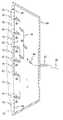
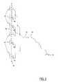
- FIG. 4is an elevation, partially broken away, showing a plurality of patch/microstrip antenna elements, for example, of the embodiment of FIG. 3;
- FIG. 5is a simplified view of a single patch antenna element polarized in a vertical direction
- FIG. 6is an elevation, similar to FIG. 4, showing a vertical array of patch antenna elements provided with static drain lines on both sides,
- FIG. 7is an elevation, similar to FIG. 6, showing static drain lines on one side of the patch antenna elements
- FIG. 8is a side elevation, similar to FIG. 3, additionally showing the static drain lines etched onto a printed circuit board;
- FIG. 9is a side elevation, similar to FIG. 8, additionally showing a metal backplane or housing and a coaxial connector.
- FIG. 1shows a conventional arrangement for a Cellular or PCS base station 20 having a tower 22 with a passive antenna 25 and ground-based electronics 24 connected to the antenna 25 by an RF cable 26 .
- Lightning arrestor(s) 28 , 30are used either after the antenna at the tower top or at the base station, before the electronics, or both.
- the arrestors 28 , 30are high voltage capacitors wired in series with the RF cable 26 . This prevents low frequency or DC current, associated with the absorbed corona energy, from a near miss lightning strike, from traveling through the RF coaxial cable into the base station electronics.
- FIG. 2shows a side view, partially in section, of a typical patch antenna system 40 , using an array of patch antenna elements (or “plates”) 42 and aperture coupling of the patch antenna elements 42 to a corporate feed 44 , at apertures (irises) 46 in a ground plane 48 .
- the corporate feed 44(shown here as a stripline structure) is shown in isometric view for ease of illustration. In a three-dimensional physical embodiment, the corporate feed would be in the same plane as the stripline coupling to the patches, etched on the same substrate (not shown in FIG. 2 ). The corporate feed could also be applied as a coaxial (cable) structure.
- the final feed outputis connected to the coaxial cable 26 which traverses the tower 25 (FIG. 1) by a connector 52 .
- the conventional lightning arrestors 28 , 30At the top and base of the tower 25 are the conventional lightning arrestors 28 , 30 . As mentioned above, these are typically large series capacitors, which can handle extremely large voltages, and act to suppress DC and low frequency currents.
- the base station electronics 24typically within a shelter (see FIG. 1 ), and comprised of amplifiers, transceivers, and modems.
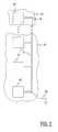
- FIG. 3shows the antenna (array) arrangement of FIG. 2, indicated by like reference numerals, and further including an antenna housing 60 (e.g., a radome 62 plus a backplane/extrusion 64 ).
- the housingis shown in FIG. 3 as a simple rectangle; however, the actual radome and backplane can take various forms and shapes.
- the radome 62is made from a dielectric material, and the backplane/extrusion 64 from a metallic material (such as aluminum).
- the interaction and functionality of the housingis typically not considered, with respect to influences from lightning (corona discharge) and static build-up.
- FIG. 3shows the general concept for an active antenna system in accordance with the invention.
- active electronic components 66are shown at various stages of the corporate feed 44 ; directly after each antenna element 42 (directly at each feed point) and/or at various stages prior to a final input/output connector 68 .
- This arrangementapplies to transmit as well as receive antennas, or to antennas used as both transmit/receive antennas.
- the active components 66can be any discrete device, or a number of discrete devices, IC's or circuits, such as amplifiers (devices or circuits), active phase shifters, RF power detectors, LNAs (Low Noise Amplifiers), etc.
- FIG. 4shows a plurality of patch/microstrip antenna elements 42 , which comprise a typical antenna.
- the configuration shownis a single column of M antenna elements 42 , however, this concept readily applies to a general (2-dimensional) M ⁇ N array of elements as well.
- These elementsare typically etched on a dielectric substrate (or “superstrate”) 70 located above the ground plane 48 containing the apertures 46 (not shown in FIG. 4) such as a floating printed circuit board (PCB) not directly connected to the ground plane 48 (i.e. an air gap between the two boards).
- This substrate 70may be a PCB (printed circuit board).
- FIG. 5shows a single patch antenna element 42 , one of the elements from FIG. 4, with the polarization of the antenna element indicated as vertical by arrows 55 . Therefore, the RF voltage is highest on the top and bottom of the patch 42 .
- the RF voltageis near zero on the symmetry line (center) 45 of the patch, as shown in FIG. 5 .
- the RF voltageis low, and increases to a maximum (at the patch resonant frequency) towards the top and bottom of the patch.
- low frequency energy and DC energy (voltage)is fairly evenly distributed across the whole patch. Therefore, this energy can be tapped off at nearly any point on the patch. It will be apparent that the same considerations would apply for other polarization directions of the patch(es), e.g., horizontal, diagonal, etc.
- FIG. 6shows one way to accomplish this.
- Metallic striplines (or coaxial lines) 75are connected at the symmetry area of the patch and serve as static drain lines or taps.
- This diagramshows taps on both sides of the patch. This construction keeps the RF characteristics balanced, and does not “skew” the radiation pattern to right or left of the patch (in this case, does not rotate the azimuth pattern to one side or the other).
- FIG. 7shows the static drain lines 75 on one side only, and a wire 80 connected from the bottom right corner of the drain line 75 , to ground.
- the groundcan be the ground plane 48 with the apertures, or the backplane 64 , or the (grounded) outer connector of the connector 52 or outer conductor of the coaxial cable 26 (to the base station).
- FIG. 6shows a connector or pin 82 on the dielectric substrate or PCB 70 which can be used to effect a similar ground connection.
- FIG. 8shows a partial side sectional view of the patch antenna system, with lightning protection static drain lines 75 , connected to ground.
- the absorbed DC or low frequency energyis directly ported to ground, rather than passing through the antenna (RF) apertures 46 , to the stripline (or coaxial) feed lines 44 , and then going through the sensitive electronics 66 .
- FIG. 9shows a more complete system, in which all internal electronics 66 are now shielded from the lightning, corona, or static (low frequency or DC) energy.
- the (metallic) ground plane 48(with apertures 46 ) is directly connected to the (metallic) backplane 64 of the system.
- This backplane 64is connected to an RF connector 52 for the coaxial cable 26 to the base station.
- the outer shield of the coaxial cable 26shunts the energy to ground.
- the backplane (or the antenna housing) 64 , as well as the patch ground plane 48are connected with each other and to form a “closed” area defining a Gaussian shield around all internal electronics. This is to ensure that no low frequency RF (at high voltage/power levels) can leak in and damage the sensitive electronics. There should not be any large holes (greater than about 1 ⁇ 2 inch), anywhere on the outer shield or shell (elements 48 and 64 in the embodiment of FIG. 9) of the system, that can “leak” low frequency or DC energy to the internal electronics. This “shell” further enhances the lightning protection arrangement for the sensitive internal electronic components 66 .
- This shield or shellcould also be made from metal mesh, with mesh size of less than ⁇ fraction (1/100 ) ⁇ th of a wavelength.
Landscapes
- Engineering & Computer Science (AREA)
- Computer Networks & Wireless Communication (AREA)
- Details Of Aerials (AREA)
- Waveguide Aerials (AREA)
- Variable-Direction Aerials And Aerial Arrays (AREA)
- Emergency Protection Circuit Devices (AREA)
Abstract
Description
Claims (38)
Priority Applications (11)
| Application Number | Priority Date | Filing Date | Title |
|---|---|---|---|
| US09/483,648US6362787B1 (en) | 1999-04-26 | 2000-01-14 | Lightning protection for an active antenna using patch/microstrip elements |
| IL140423AIL140423A (en) | 2000-01-14 | 2000-12-19 | Lightning protection for an active antenna using patch/microstrip elements |
| AU72505/00AAU777157C (en) | 2000-01-14 | 2000-12-22 | Lightning protection for an active antenna using patch/microstrip elements |
| CA002329668ACA2329668C (en) | 2000-01-14 | 2000-12-27 | Lightning protection for an active antenna using patch/microstrip elements |
| JP2001002369AJP2001237634A (en) | 2000-01-14 | 2001-01-10 | Active antenna system having method and means for lightning protection for active antenna using patch/ microstrip element |
| DE60122029TDE60122029T2 (en) | 2000-01-14 | 2001-01-11 | Lightning protection for an active antenna with patch / microstrip elements |
| EP01100096AEP1117147B1 (en) | 2000-01-14 | 2001-01-11 | Lightning protection for an active antenna using patch/microstrip elements |
| AT01100096TATE336088T1 (en) | 2000-01-14 | 2001-01-11 | LIGHTNING PROTECTION FOR AN ACTIVE ANTENNA WITH PATCH/MICROSTRIP ELEMENTS |
| BR0100069-1ABR0100069A (en) | 2000-01-14 | 2001-01-12 | Lightning protection for an active antenna using splice / micro band elements |
| KR1020010002071AKR20010086337A (en) | 2000-01-14 | 2001-01-13 | Lightning protection for an active antenna using patch/microstrip elements |
| CNB011012684ACN1213510C (en) | 2000-01-14 | 2001-01-15 | Lightning protection of using plaster/micro-stripe unit active antenna |
Applications Claiming Priority (3)
| Application Number | Priority Date | Filing Date | Title |
|---|---|---|---|
| US09/299,850US6583763B2 (en) | 1999-04-26 | 1999-04-26 | Antenna structure and installation |
| US09/422,418US6597325B2 (en) | 1999-04-26 | 1999-10-21 | Transmit/receive distributed antenna systems |
| US09/483,648US6362787B1 (en) | 1999-04-26 | 2000-01-14 | Lightning protection for an active antenna using patch/microstrip elements |
Related Parent Applications (1)
| Application Number | Title | Priority Date | Filing Date |
|---|---|---|---|
| US09/299,850Continuation-In-PartUS6583763B2 (en) | 1999-04-26 | 1999-04-26 | Antenna structure and installation |
Publications (1)
| Publication Number | Publication Date |
|---|---|
| US6362787B1true US6362787B1 (en) | 2002-03-26 |
Family
ID=23920936
Family Applications (1)
| Application Number | Title | Priority Date | Filing Date |
|---|---|---|---|
| US09/483,648Expired - Fee RelatedUS6362787B1 (en) | 1999-04-26 | 2000-01-14 | Lightning protection for an active antenna using patch/microstrip elements |
Country Status (11)
| Country | Link |
|---|---|
| US (1) | US6362787B1 (en) |
| EP (1) | EP1117147B1 (en) |
| JP (1) | JP2001237634A (en) |
| KR (1) | KR20010086337A (en) |
| CN (1) | CN1213510C (en) |
| AT (1) | ATE336088T1 (en) |
| AU (1) | AU777157C (en) |
| BR (1) | BR0100069A (en) |
| CA (1) | CA2329668C (en) |
| DE (1) | DE60122029T2 (en) |
| IL (1) | IL140423A (en) |
Cited By (5)
| Publication number | Priority date | Publication date | Assignee | Title |
|---|---|---|---|---|
| EP1708120A1 (en)* | 2005-03-29 | 2006-10-04 | Accu-Sort Systems, Inc. | RFID conveyor system |
| US20070085746A1 (en)* | 2005-10-19 | 2007-04-19 | Lite-On Technology Corp. | Electrostatic Discharge Protection Receiving System |
| US20150200434A1 (en)* | 2014-01-15 | 2015-07-16 | Honeywell International Inc. | Anti-lightning combined-stripline-circuit system |
| CN107834199A (en)* | 2017-12-01 | 2018-03-23 | 成都信息工程大学 | A kind of intelligent active lightning protection antenna and lightning-protection system |
| WO2025038381A1 (en)* | 2023-08-11 | 2025-02-20 | Viasat, Inc. | Radiation-induced charge dispersion path |
Families Citing this family (9)
| Publication number | Priority date | Publication date | Assignee | Title |
|---|---|---|---|---|
| RU2271813C1 (en)* | 2004-10-18 | 2006-03-20 | Государственное образовательное учреждение высшего профессионального образования "Нижегородская Государственная Медицинская академия" МЗ РФ (ГОУ ВПО НижГМА) | Method for correction of cancer carrier liver morphological state |
| GB2440192B (en)* | 2006-07-17 | 2011-05-04 | Ubidyne Inc | Antenna array system |
| FR2993103B1 (en)* | 2012-07-05 | 2014-08-15 | Dassault Aviat | ANTENNA ASSEMBLY |
| CN103454569A (en)* | 2013-09-23 | 2013-12-18 | 镇江艾科半导体有限公司 | Semiconductor chip test board |
| KR101929348B1 (en)* | 2017-04-21 | 2018-12-14 | 주식회사 감마누 | Low PIMD base station antenna having active elements |
| CN109244654B (en)* | 2018-08-20 | 2022-09-27 | 中国电力科学研究院有限公司 | Patch antenna for television interference measurement, television interference measurement device and method |
| CN109728575B (en)* | 2018-12-21 | 2020-10-23 | 中电科航空电子有限公司 | Airborne antenna lightning protection circuit system |
| DE202019101043U1 (en) | 2019-02-22 | 2020-05-25 | Ericsson Ab | Phase shifter module arrangement for use in a mobile radio antenna |
| CN114447583B (en)* | 2019-08-23 | 2023-09-01 | 华为技术有限公司 | Antenna and electronic equipment |
Citations (44)
| Publication number | Priority date | Publication date | Assignee | Title |
|---|---|---|---|---|
| US4124852A (en) | 1977-01-24 | 1978-11-07 | Raytheon Company | Phased power switching system for scanning antenna array |
| US4360813A (en) | 1980-03-19 | 1982-11-23 | The Boeing Company | Power combining antenna structure |
| US4566013A (en) | 1983-04-01 | 1986-01-21 | The United States Of America As Represented By The Secretary Of The Navy | Coupled amplifier module feed networks for phased array antennas |
| US4689631A (en) | 1985-05-28 | 1987-08-25 | American Telephone And Telegraph Company, At&T Bell Laboratories | Space amplifier |
| US4825172A (en) | 1987-03-30 | 1989-04-25 | Hughes Aircraft Company | Equal power amplifier system for active phase array antenna and method of arranging same |
| US4849763A (en) | 1987-04-23 | 1989-07-18 | Hughes Aircraft Company | Low sidelobe phased array antenna using identical solid state modules |
| US4890110A (en) | 1988-01-12 | 1989-12-26 | Nec Corporation | Microwave landing system |
| US5034752A (en) | 1989-07-04 | 1991-07-23 | Thomson Csf | Multiple-beam antenna system with active modules and digital beam-forming |
| US5061939A (en)* | 1989-05-23 | 1991-10-29 | Harada Kogyo Kabushiki Kaisha | Flat-plate antenna for use in mobile communications |
| US5230080A (en) | 1990-03-09 | 1993-07-20 | Compagnie Generale Des Matieres Nucleaires | Ultra-high frequency communication installation |
| US5248980A (en) | 1991-04-05 | 1993-09-28 | Alcatel Espace | Spacecraft payload architecture |
| US5280297A (en) | 1992-04-06 | 1994-01-18 | General Electric Co. | Active reflectarray antenna for communication satellite frequency re-use |
| US5327150A (en) | 1993-03-03 | 1994-07-05 | Hughes Aircraft Company | Phased array antenna for efficient radiation of microwave and thermal energy |
| US5379455A (en) | 1991-02-28 | 1995-01-03 | Hewlett-Packard Company | Modular distributed antenna system |
| US5412414A (en) | 1988-04-08 | 1995-05-02 | Martin Marietta Corporation | Self monitoring/calibrating phased array radar and an interchangeable, adjustable transmit/receive sub-assembly |
| WO1995034102A1 (en) | 1994-06-03 | 1995-12-14 | Telefonaktiebolaget Lm Ericsson | Microstrip antenna array |
| US5513176A (en) | 1990-12-07 | 1996-04-30 | Qualcomm Incorporated | Dual distributed antenna system |
| US5548813A (en) | 1994-03-24 | 1996-08-20 | Ericsson Inc. | Phased array cellular base station and associated methods for enhanced power efficiency |
| US5596329A (en) | 1993-08-12 | 1997-01-21 | Northern Telecom Limited | Base station antenna arrangement |
| US5604462A (en) | 1995-11-17 | 1997-02-18 | Lucent Technologies Inc. | Intermodulation distortion detection in a power shared amplifier network |
| US5619210A (en) | 1994-04-08 | 1997-04-08 | Ericsson Inc. | Large phased-array communications satellite |
| US5621422A (en)* | 1994-08-22 | 1997-04-15 | Wang-Tripp Corporation | Spiral-mode microstrip (SMM) antennas and associated methods for exciting, extracting and multiplexing the various spiral modes |
| US5644622A (en) | 1992-09-17 | 1997-07-01 | Adc Telecommunications, Inc. | Cellular communications system with centralized base stations and distributed antenna units |
| US5646631A (en) | 1995-12-15 | 1997-07-08 | Lucent Technologies Inc. | Peak power reduction in power sharing amplifier networks |
| US5659322A (en) | 1992-12-04 | 1997-08-19 | Alcatel N.V. | Variable synthesized polarization active antenna |
| US5710804A (en) | 1995-07-19 | 1998-01-20 | Pcs Solutions, Llc | Service protection enclosure for and method of constructing a remote wireless telecommunication site |
| US5714957A (en) | 1993-08-12 | 1998-02-03 | Northern Telecom Limited | Base station antenna arrangement |
| US5724666A (en) | 1994-03-24 | 1998-03-03 | Ericsson Inc. | Polarization diversity phased array cellular base station and associated methods |
| WO1998009372A1 (en) | 1996-08-27 | 1998-03-05 | Telefonaktiebolaget Lm Ericsson (Publ) | Method of and apparatus for filtering intermodulation products in a radiocommunication system |
| WO1998011626A1 (en) | 1996-09-16 | 1998-03-19 | Raytheon Company | Antenna system for enhancing the coverage area, range and reliability of wireless base stations |
| US5751250A (en) | 1995-10-13 | 1998-05-12 | Lucent Technologies, Inc. | Low distortion power sharing amplifier network |
| US5770970A (en) | 1995-08-30 | 1998-06-23 | Matsushita Electric Industrial Co., Ltd. | Transmitter of wireless system and high frequency power amplifier used therein |
| US5802173A (en) | 1991-01-15 | 1998-09-01 | Rogers Cable Systems Limited | Radiotelephony system |
| US5809395A (en) | 1991-01-15 | 1998-09-15 | Rogers Cable Systems Limited | Remote antenna driver for a radio telephony system |
| US5832389A (en) | 1994-03-24 | 1998-11-03 | Ericsson Inc. | Wideband digitization systems and methods for cellular radiotelephones |
| WO1998050981A1 (en) | 1997-05-07 | 1998-11-12 | Telefonaktiebolaget Lm Ericsson (Publ) | Radio antenna system |
| US5854611A (en) | 1995-07-24 | 1998-12-29 | Lucent Technologies Inc. | Power shared linear amplifier network |
| US5987335A (en)* | 1997-09-24 | 1999-11-16 | Lucent Technologies Inc. | Communication system comprising lightning protection |
| US6008763A (en)* | 1996-05-13 | 1999-12-28 | Allgon Ab | Flat antenna |
| US6043790A (en) | 1997-03-24 | 2000-03-28 | Telefonaktiebolaget Lm Ericsson | Integrated transmit/receive antenna with arbitrary utilization of the antenna aperture |
| US6072434A (en)* | 1997-02-04 | 2000-06-06 | Lucent Technologies Inc. | Aperture-coupled planar inverted-F antenna |
| US6091360A (en) | 1997-08-20 | 2000-07-18 | Hollandse Signaalapparaten B.V. | Antenna system |
| US6104935A (en) | 1997-05-05 | 2000-08-15 | Nortel Networks Corporation | Down link beam forming architecture for heavily overlapped beam configuration |
| US6140976A (en) | 1999-09-07 | 2000-10-31 | Motorola, Inc. | Method and apparatus for mitigating array antenna performance degradation caused by element failure |
Family Cites Families (2)
| Publication number | Priority date | Publication date | Assignee | Title |
|---|---|---|---|---|
| JP2735727B2 (en)* | 1992-01-23 | 1998-04-02 | 三菱電機株式会社 | Array antenna device |
| US6008750A (en)* | 1997-02-11 | 1999-12-28 | Decatur Electronics, Inc. | Microwave transceiver utilizing a microstrip antenna |
- 2000
- 2000-01-14USUS09/483,648patent/US6362787B1/ennot_activeExpired - Fee Related
- 2000-12-19ILIL140423Apatent/IL140423A/ennot_activeIP Right Cessation
- 2000-12-22AUAU72505/00Apatent/AU777157C/ennot_activeCeased
- 2000-12-27CACA002329668Apatent/CA2329668C/ennot_activeExpired - Fee Related
- 2001
- 2001-01-10JPJP2001002369Apatent/JP2001237634A/enactivePending
- 2001-01-11DEDE60122029Tpatent/DE60122029T2/ennot_activeExpired - Fee Related
- 2001-01-11ATAT01100096Tpatent/ATE336088T1/ennot_activeIP Right Cessation
- 2001-01-11EPEP01100096Apatent/EP1117147B1/ennot_activeExpired - Lifetime
- 2001-01-12BRBR0100069-1Apatent/BR0100069A/ennot_activeIP Right Cessation
- 2001-01-13KRKR1020010002071Apatent/KR20010086337A/ennot_activeAbandoned
- 2001-01-15CNCNB011012684Apatent/CN1213510C/ennot_activeExpired - Fee Related
Patent Citations (45)
| Publication number | Priority date | Publication date | Assignee | Title |
|---|---|---|---|---|
| US4124852A (en) | 1977-01-24 | 1978-11-07 | Raytheon Company | Phased power switching system for scanning antenna array |
| US4360813A (en) | 1980-03-19 | 1982-11-23 | The Boeing Company | Power combining antenna structure |
| US4566013A (en) | 1983-04-01 | 1986-01-21 | The United States Of America As Represented By The Secretary Of The Navy | Coupled amplifier module feed networks for phased array antennas |
| US4689631A (en) | 1985-05-28 | 1987-08-25 | American Telephone And Telegraph Company, At&T Bell Laboratories | Space amplifier |
| US4825172A (en) | 1987-03-30 | 1989-04-25 | Hughes Aircraft Company | Equal power amplifier system for active phase array antenna and method of arranging same |
| US4849763A (en) | 1987-04-23 | 1989-07-18 | Hughes Aircraft Company | Low sidelobe phased array antenna using identical solid state modules |
| US4890110A (en) | 1988-01-12 | 1989-12-26 | Nec Corporation | Microwave landing system |
| US5412414A (en) | 1988-04-08 | 1995-05-02 | Martin Marietta Corporation | Self monitoring/calibrating phased array radar and an interchangeable, adjustable transmit/receive sub-assembly |
| US5061939A (en)* | 1989-05-23 | 1991-10-29 | Harada Kogyo Kabushiki Kaisha | Flat-plate antenna for use in mobile communications |
| US5034752A (en) | 1989-07-04 | 1991-07-23 | Thomson Csf | Multiple-beam antenna system with active modules and digital beam-forming |
| US5230080A (en) | 1990-03-09 | 1993-07-20 | Compagnie Generale Des Matieres Nucleaires | Ultra-high frequency communication installation |
| US5513176A (en) | 1990-12-07 | 1996-04-30 | Qualcomm Incorporated | Dual distributed antenna system |
| US5809395A (en) | 1991-01-15 | 1998-09-15 | Rogers Cable Systems Limited | Remote antenna driver for a radio telephony system |
| US5802173A (en) | 1991-01-15 | 1998-09-01 | Rogers Cable Systems Limited | Radiotelephony system |
| US5379455A (en) | 1991-02-28 | 1995-01-03 | Hewlett-Packard Company | Modular distributed antenna system |
| US5248980A (en) | 1991-04-05 | 1993-09-28 | Alcatel Espace | Spacecraft payload architecture |
| US5280297A (en) | 1992-04-06 | 1994-01-18 | General Electric Co. | Active reflectarray antenna for communication satellite frequency re-use |
| US5644622A (en) | 1992-09-17 | 1997-07-01 | Adc Telecommunications, Inc. | Cellular communications system with centralized base stations and distributed antenna units |
| US5659322A (en) | 1992-12-04 | 1997-08-19 | Alcatel N.V. | Variable synthesized polarization active antenna |
| US5327150A (en) | 1993-03-03 | 1994-07-05 | Hughes Aircraft Company | Phased array antenna for efficient radiation of microwave and thermal energy |
| US5596329A (en) | 1993-08-12 | 1997-01-21 | Northern Telecom Limited | Base station antenna arrangement |
| US5714957A (en) | 1993-08-12 | 1998-02-03 | Northern Telecom Limited | Base station antenna arrangement |
| US5832389A (en) | 1994-03-24 | 1998-11-03 | Ericsson Inc. | Wideband digitization systems and methods for cellular radiotelephones |
| US5548813A (en) | 1994-03-24 | 1996-08-20 | Ericsson Inc. | Phased array cellular base station and associated methods for enhanced power efficiency |
| US5724666A (en) | 1994-03-24 | 1998-03-03 | Ericsson Inc. | Polarization diversity phased array cellular base station and associated methods |
| US5619210A (en) | 1994-04-08 | 1997-04-08 | Ericsson Inc. | Large phased-array communications satellite |
| WO1995034102A1 (en) | 1994-06-03 | 1995-12-14 | Telefonaktiebolaget Lm Ericsson | Microstrip antenna array |
| US5621422A (en)* | 1994-08-22 | 1997-04-15 | Wang-Tripp Corporation | Spiral-mode microstrip (SMM) antennas and associated methods for exciting, extracting and multiplexing the various spiral modes |
| US5710804A (en) | 1995-07-19 | 1998-01-20 | Pcs Solutions, Llc | Service protection enclosure for and method of constructing a remote wireless telecommunication site |
| US5854611A (en) | 1995-07-24 | 1998-12-29 | Lucent Technologies Inc. | Power shared linear amplifier network |
| US5770970A (en) | 1995-08-30 | 1998-06-23 | Matsushita Electric Industrial Co., Ltd. | Transmitter of wireless system and high frequency power amplifier used therein |
| US5751250A (en) | 1995-10-13 | 1998-05-12 | Lucent Technologies, Inc. | Low distortion power sharing amplifier network |
| US5604462A (en) | 1995-11-17 | 1997-02-18 | Lucent Technologies Inc. | Intermodulation distortion detection in a power shared amplifier network |
| US5646631A (en) | 1995-12-15 | 1997-07-08 | Lucent Technologies Inc. | Peak power reduction in power sharing amplifier networks |
| US6008763A (en)* | 1996-05-13 | 1999-12-28 | Allgon Ab | Flat antenna |
| US5862459A (en) | 1996-08-27 | 1999-01-19 | Telefonaktiebolaget Lm Ericsson | Method of and apparatus for filtering intermodulation products in a radiocommunication system |
| WO1998009372A1 (en) | 1996-08-27 | 1998-03-05 | Telefonaktiebolaget Lm Ericsson (Publ) | Method of and apparatus for filtering intermodulation products in a radiocommunication system |
| WO1998011626A1 (en) | 1996-09-16 | 1998-03-19 | Raytheon Company | Antenna system for enhancing the coverage area, range and reliability of wireless base stations |
| US6072434A (en)* | 1997-02-04 | 2000-06-06 | Lucent Technologies Inc. | Aperture-coupled planar inverted-F antenna |
| US6043790A (en) | 1997-03-24 | 2000-03-28 | Telefonaktiebolaget Lm Ericsson | Integrated transmit/receive antenna with arbitrary utilization of the antenna aperture |
| US6104935A (en) | 1997-05-05 | 2000-08-15 | Nortel Networks Corporation | Down link beam forming architecture for heavily overlapped beam configuration |
| WO1998050981A1 (en) | 1997-05-07 | 1998-11-12 | Telefonaktiebolaget Lm Ericsson (Publ) | Radio antenna system |
| US6091360A (en) | 1997-08-20 | 2000-07-18 | Hollandse Signaalapparaten B.V. | Antenna system |
| US5987335A (en)* | 1997-09-24 | 1999-11-16 | Lucent Technologies Inc. | Communication system comprising lightning protection |
| US6140976A (en) | 1999-09-07 | 2000-10-31 | Motorola, Inc. | Method and apparatus for mitigating array antenna performance degradation caused by element failure |
Cited By (16)
| Publication number | Priority date | Publication date | Assignee | Title |
|---|---|---|---|---|
| US7538675B2 (en) | 2005-03-29 | 2009-05-26 | Accu-Sort Systems, Inc. | RFID conveyor system |
| US7576655B2 (en) | 2005-03-29 | 2009-08-18 | Accu-Sort Systems, Inc. | RFID conveyor system and method |
| US20060238351A1 (en)* | 2005-03-29 | 2006-10-26 | Hillegass Raymond R | RFID conveyor system |
| US20060244609A1 (en)* | 2005-03-29 | 2006-11-02 | Zhong-Min Liu | RFID conveyor system |
| US20060250253A1 (en)* | 2005-03-29 | 2006-11-09 | Zhong-Min Liu | RFID conveyor system and method |
| US7592915B2 (en) | 2005-03-29 | 2009-09-22 | Accu-Sort Systems, Inc. | RFID conveyor system |
| US20060232422A1 (en)* | 2005-03-29 | 2006-10-19 | Zhong-Min Liu | RFID conveyor system |
| US7518513B2 (en) | 2005-03-29 | 2009-04-14 | Accu-Sort Systems, Inc. | RFID conveyor system |
| EP1708120A1 (en)* | 2005-03-29 | 2006-10-04 | Accu-Sort Systems, Inc. | RFID conveyor system |
| GB2431520A (en)* | 2005-10-19 | 2007-04-25 | Lite On Technology Corp | Antenna with built-in electrostatic discharge protection |
| US20070085746A1 (en)* | 2005-10-19 | 2007-04-19 | Lite-On Technology Corp. | Electrostatic Discharge Protection Receiving System |
| US20150200434A1 (en)* | 2014-01-15 | 2015-07-16 | Honeywell International Inc. | Anti-lightning combined-stripline-circuit system |
| US9614268B2 (en)* | 2014-01-15 | 2017-04-04 | Honeywell International Inc. | Anti-lightning combined-stripline-circuit system |
| RU2681370C2 (en)* | 2014-01-15 | 2019-03-06 | Ханивелл Интернешнл Инк. | Anti-lightning-combined-stripline-circuit system |
| CN107834199A (en)* | 2017-12-01 | 2018-03-23 | 成都信息工程大学 | A kind of intelligent active lightning protection antenna and lightning-protection system |
| WO2025038381A1 (en)* | 2023-08-11 | 2025-02-20 | Viasat, Inc. | Radiation-induced charge dispersion path |
Also Published As
| Publication number | Publication date |
|---|---|
| DE60122029T2 (en) | 2007-02-22 |
| IL140423A (en) | 2006-08-20 |
| EP1117147B1 (en) | 2006-08-09 |
| DE60122029D1 (en) | 2006-09-21 |
| KR20010086337A (en) | 2001-09-10 |
| EP1117147A3 (en) | 2003-10-15 |
| CA2329668A1 (en) | 2001-07-14 |
| EP1117147A2 (en) | 2001-07-18 |
| IL140423A0 (en) | 2002-02-10 |
| AU7250500A (en) | 2001-07-19 |
| BR0100069A (en) | 2001-08-21 |
| AU777157B2 (en) | 2004-10-07 |
| AU777157C (en) | 2005-07-21 |
| CA2329668C (en) | 2003-08-19 |
| CN1306318A (en) | 2001-08-01 |
| ATE336088T1 (en) | 2006-09-15 |
| CN1213510C (en) | 2005-08-03 |
| JP2001237634A (en) | 2001-08-31 |
Similar Documents
| Publication | Publication Date | Title |
|---|---|---|
| US20220045440A1 (en) | Integrated filter radiator for a multiband antenna | |
| US6292154B1 (en) | Antenna device | |
| US4916457A (en) | Printed-circuit crossed-slot antenna | |
| US6362787B1 (en) | Lightning protection for an active antenna using patch/microstrip elements | |
| US6243247B1 (en) | Stripline transient protection device | |
| US6359588B1 (en) | Patch antenna | |
| US7750861B2 (en) | Hybrid antenna including spiral antenna and periodic array, and associated methods | |
| US11005162B2 (en) | Antenna structure of wireless communication device | |
| US20020015000A1 (en) | Folded mono-bow antennas and antenna systems for use in cellular and other wireless communications systems | |
| US5742258A (en) | Low intermodulation electromagnetic feed cellular antennas | |
| CN210074170U (en) | High frequency module | |
| US8502747B2 (en) | Dipole antenna assembly | |
| US20030112200A1 (en) | Horizontally polarized printed circuit antenna array | |
| US12381334B2 (en) | Antenna device, array of antenna devices, and base station with antenna device | |
| US12199345B2 (en) | Base station antennas having compact dual-polarized box dipole radiating elements therein that support high band cloaking | |
| US10707568B2 (en) | Antenna structure | |
| US12334648B2 (en) | Dual mode antenna arrangement | |
| WO2021197400A1 (en) | A patch antenna | |
| AU2020401268A1 (en) | Omnidirectional horizontally polarized antenna with high current protection | |
| CN217788794U (en) | Antenna module with large scanning angle and electronic equipment | |
| US11557823B2 (en) | Antenna component | |
| KR102529334B1 (en) | MIMO antenna and MIMO antenna apparatus having the same | |
| US12027745B2 (en) | Hybrid coupler and method for manufacturing hybrid couplers | |
| CN212366219U (en) | directional antenna | |
| WO2025196473A1 (en) | Low band crossed-dipole antenna with meandered arms |
Legal Events
| Date | Code | Title | Description |
|---|---|---|---|
| AS | Assignment | Owner name:ANDREW CORPORATION, ILLINOIS Free format text:ASSIGNMENT OF ASSIGNORS INTEREST;ASSIGNORS:JUDD, MANO D.;MONTE, THOMAS D.;REEL/FRAME:010527/0490;SIGNING DATES FROM 20000106 TO 20000112 | |
| FPAY | Fee payment | Year of fee payment:4 | |
| AS | Assignment | Owner name:BANK OF AMERICA, N.A., AS ADMINISTRATIVE AGENT, CA Free format text:SECURITY AGREEMENT;ASSIGNORS:COMMSCOPE, INC. OF NORTH CAROLINA;ALLEN TELECOM, LLC;ANDREW CORPORATION;REEL/FRAME:020362/0241 Effective date:20071227 Owner name:BANK OF AMERICA, N.A., AS ADMINISTRATIVE AGENT,CAL Free format text:SECURITY AGREEMENT;ASSIGNORS:COMMSCOPE, INC. OF NORTH CAROLINA;ALLEN TELECOM, LLC;ANDREW CORPORATION;REEL/FRAME:020362/0241 Effective date:20071227 | |
| AS | Assignment | Owner name:ANDREW LLC, NORTH CAROLINA Free format text:CHANGE OF NAME;ASSIGNOR:ANDREW CORPORATION;REEL/FRAME:021805/0044 Effective date:20080827 | |
| REMI | Maintenance fee reminder mailed | ||
| LAPS | Lapse for failure to pay maintenance fees | ||
| STCH | Information on status: patent discontinuation | Free format text:PATENT EXPIRED DUE TO NONPAYMENT OF MAINTENANCE FEES UNDER 37 CFR 1.362 | |
| FP | Lapsed due to failure to pay maintenance fee | Effective date:20100326 | |
| AS | Assignment | Owner name:ANDREW LLC (F/K/A ANDREW CORPORATION), NORTH CAROL Free format text:PATENT RELEASE;ASSIGNOR:BANK OF AMERICA, N.A., AS ADMINISTRATIVE AGENT;REEL/FRAME:026039/0005 Effective date:20110114 Owner name:COMMSCOPE, INC. OF NORTH CAROLINA, NORTH CAROLINA Free format text:PATENT RELEASE;ASSIGNOR:BANK OF AMERICA, N.A., AS ADMINISTRATIVE AGENT;REEL/FRAME:026039/0005 Effective date:20110114 Owner name:ALLEN TELECOM LLC, NORTH CAROLINA Free format text:PATENT RELEASE;ASSIGNOR:BANK OF AMERICA, N.A., AS ADMINISTRATIVE AGENT;REEL/FRAME:026039/0005 Effective date:20110114 |