US6362649B1 - Field programmable gate array with mask programmed input and output buffers - Google Patents
Field programmable gate array with mask programmed input and output buffersDownload PDFInfo
- Publication number
- US6362649B1 US6362649B1US09/286,128US28612899AUS6362649B1US 6362649 B1US6362649 B1US 6362649B1US 28612899 AUS28612899 AUS 28612899AUS 6362649 B1US6362649 B1US 6362649B1
- Authority
- US
- United States
- Prior art keywords
- input
- output
- ones
- pads
- interconnect
- Prior art date
- Legal status (The legal status is an assumption and is not a legal conclusion. Google has not performed a legal analysis and makes no representation as to the accuracy of the status listed.)
- Expired - Fee Related
Links
Images


Classifications
- H—ELECTRICITY
- H03—ELECTRONIC CIRCUITRY
- H03K—PULSE TECHNIQUE
- H03K19/00—Logic circuits, i.e. having at least two inputs acting on one output; Inverting circuits
- H03K19/02—Logic circuits, i.e. having at least two inputs acting on one output; Inverting circuits using specified components
- H03K19/173—Logic circuits, i.e. having at least two inputs acting on one output; Inverting circuits using specified components using elementary logic circuits as components
- H03K19/177—Logic circuits, i.e. having at least two inputs acting on one output; Inverting circuits using specified components using elementary logic circuits as components arranged in matrix form
- H03K19/1778—Structural details for adapting physical parameters
- H03K19/17788—Structural details for adapting physical parameters for input/output [I/O] voltages
Definitions
- the present inventionrelates to input and output buffers in an integrated circuit. More particularly, the present invention relates an integrated circuit having a field programmable gate array (FPGA) portion and a mask programmable portion, wherein the mask programmable portion provides specialized input and output buffer functions to the integrated circuit.
- FPGAfield programmable gate array
- signalsare transferred into and out of the die by input and output buffers, respectively, configured as part of the integrated circuit within the die.
- the input and output buffersgenerally perform relatively standard functions that are useful on all inputs and outputs, however, any or all the input and output buffers may also be configured to perform a variety of specialized functions including voltage gain, current gain, level translation, delay, signal isolation or hysteresis.
- an FPGAis a collection of groups of gates partitioned into logic function modules which may be configured by user programmable interconnect elements to implement a large variety of digital logic functions.
- a programmable interconnect architecturecomprising a plurality of initially uncommitted interconnect conductors is superimposed over the array of logic function modules to enable custom connections to be made among the input and outputs of individual ones of logic function modules by user programmable elements to form digital circuits.
- the user programmable interconnect elements in both the logic function modules and the interconnect architecturemay take several forms, such as one time programmable antifuse elements, transistors, RAM cells, etc. These forms of user programmable interconnect elements are well known to those of ordinary skill in the art.
- logic function modules typically on the periphery of the arrayare configured to provide the input and output buffers having any or all of the functions recited above.
- the input and output buffersare connectable to the inputs and the outputs of the logic function modules via the programmable interconnect structure to allow signals to flow into and out of the programmed logic modules comprising the digital circuits of the FPGA for processing by these digital circuits.
- the logic function modulesmay be any one of a variety of circuits, including, for example, the logic modules disclosed in U.S. Pat. No. 4,758,745 to El Gamal, et al., U.S. Pat. No. 4,873,459 to El Gamal, et al., U.S. Pat. No. 4,910,417 to El Gamal, et al., U.S. Pat. No. 5,015,885 to El Gamal, et al., U.S. Pat. No. 5,451,887 to El Ayat, et al., and U.S. Pat. No. 5,477,165 to El Ayat, et al., U.S. Pat. No.
- the logic function modules which are provided to implement functions which are not selected for a particular input or output pinadd additional capacitance and resistive delay.
- design choiceshave been made in the prior art wherein only a selected number of input and output buffer functions are provided to the inputs and outputs of the integrated circuit die.
- An example of such an input buffer function inputincludes an input buffer having analog inputs.
- An example of such an output bufferincludes an output buffer that can be connected to a voltage substantially above V cc .
- a mask programmed portion of an integrated circuitprovides some of the input and output buffer functions to an FPGA portion of the integrated circuit to provide additional functional capability to the I/O buffers, and improves the flexibility, signal isolation, speed and power management of the FPGA architecture.
- the mask programmed portioncomprises N-channel and P-channel MOS transistors that can be connected together to implement almost any type of I/O buffer function conceivable in CMOS technology.
- an integrated circuit dieis partitioned into an FPGA portion and a mask programmable portion.
- logic modulesare connected to an interconnect structure comprising interconnect conductors.
- standard FPGA input buffersincluding for example level translation and power down
- a standard FPGA output bufferincluding a large drive and tri-state capability are disposed in the FPGA portion of the integrated circuit. It should be appreciated, however, that the functions implemented in the standard input and output buffers will depend upon the input and output functions required by the FPGA and the input and output functions provided by the mask programmable portion of the integrated circuit.
- interconnect conductorsspan both the FPGA portion and the masked programmed portion to connect the FPGA portion to the input and output buffers disposed in the mask programmed portion.
- the interconnect conductorsform intersections with the interconnect architecture formed by the interconnect conductors in the FPGA portion of the integrated circuit.
- user programmable interconnect elementssuch as a one time programmable antifuse element, transistors, RAM cells, etc. The use of programmable interconnect elements are employed to selectively connect the interconnect conductors to the interconnect architecture of the FPGA portion.
- the input and/or output buffers of the mask programmable portionmay either be connected to shared Vcc and ground power busses and/or be segregated to certain Vcc and ground power bus portions that are isolated from one another. Further, dedicated Vcc and ground power pads for certain I/O locations may provide selected input and/or output buffers separate busses to I/O pins.
- I/O buffer function circuits to be described hereinmay be provided to a single I/O pin or several I/O pins in the masked programmed portion of the integrated circuit, and the choice of the I/O buffers circuits to be included in the mask programmed portion will depend upon the I/O needs of the end user of the circuit. Accordingly, in the present inventions a variety of integrated circuits, each having a different mask programmed portion and the same general FPGA portion, are contemplated.
- FIG. 1is block diagram of an integrated circuit having an FPGA portion and a mask programmed portion according to the present invention.
- FIG. 2Aillustrates an FPGA with input and output buffers connected to common set of power busses according to the prior art.
- FIG. 2Billustrates input and output buffers connected to dedicated power buses in a mask programmable portion of an integrated circuit according to the present invention.
- FIG. 3Ais an input buffer implemented as a comparator in a mask programmable portion of an integrated circuit according to the present invention.
- FIG. 3Bis an input buffer implemented with a multiplexing function in a mask programmable portion of an integrated circuit according to the present invention.
- FIG. 4Ais an input buffer compatible with 74HC/AC technologies (“CMOS”) according to the prior art.
- CMOS74HC/AC technologies
- FIG. 4Bis an input buffer compatible with 74HCT/ACT/F/AS technologies (“TTL”) according to the prior art.
- FIG. 4Cis an input buffer compatible with either 74HC/AC or 74HCT/ACT/F/AS technologies, (“CMOS”) or (“TTL”), implemented in a mask programmable portion or an FPGA portion of an integrated circuit according to the present invention.
- CMOS74HCT/ACT/F/AS technologies
- TTLTTL
- FIG. 5is an input buffer implemented with a Schmitt trigger function in a mask programmable portion of an integrated circuit according to the present invention.
- FIG. 6is an output buffer implemented for low power and noise operation in a mask programmable portion of an integrated circuit according to the present invention.
- FIG. 7Ais an output buffer having a standard output totem pole stage according to the prior art.
- FIG. 7Bis an output buffer having a N-channel MOS transistor in an output totem pole stage configured as an open drain structure in a mask programmable portion of an integrated circuit according to the present invention.
- a mask programmed (i.e., dedicated) portion of an integrated circuitprovides some of the input and output (I/O) buffer functions to an FPGA portion of the integrated circuit.
- I/O buffer functionsConventionally all the I/O buffer functions of an FPGA are provided by I/O buffers configured by inputs from the logic modules of the FPGA.
- Mask programming some of the I/O buffer functions in an FPGAprovides additional functional capability to the I/O buffers.
- the mask programmed portioncomprises N-channel and P-channel MOS transistors that can be connected together to implement almost any type of I/O buffer function conceivable in CMOS technology. It should be appreciated that technologies other than CMOS are available for implementing the masked programmed portion of the present invention.
- I/O buffer function circuits to be described hereinmay be provided to a single I/O pin or several I/O pins in the masked programmed portion of the integrated circuit.
- the choice of the I/O buffers circuits to be included in the mask programmed portionwill depend upon the I/O needs of the end user of the circuit. Accordingly, a variety of integrated circuits, each having a different mask programmed portion and the same general FPGA portion, are contemplated by the present invention.
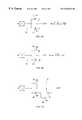
- FIG. 1a block diagram depicts the hybrid FPGA and mask programmable architecture according to the present invention.
- an integrated circuit die 10is partitioned into an FPGA portion 12 and a mask programmable portion 14 .
- the present inventionis not limited by the particular physical layout of the partitioning of the FPGA portion 12 and the mask programmable portion 14 shown in the integrated circuit 10 .
- exemplary logic modules 16 - 1 and 16 - 2are connected to an interconnect structure comprising interconnect conductors 18 - 1 through 18 - 5 .
- the interconnect conductors 18 - 1 through 18 - 5represent a wide variety of interconnection schemes for connecting logic modules in an FPGA.
- the present inventionis not limited to any specific interconnect architecture employed in FPGA.
- the various interconnection schemes available for interconnecting logic modules and FPGAwill not be disclosed herein.
- Numerous examples of interconnection schemes which are suitable for use in conjunction with the present inventionare well known to those of ordinary skill in the art.
- Different interconnect architectures including segmented interconnect architecturesare well known to those of ordinary in the art, and a non-exhaustive list of such interconnect schemes is represented by the interconnect schemes referred to the above discussed prior art section.
- logic function module designswhich are available to be employed in the present invention period.
- the present inventionis not limited to any specific logic module design employed in FPGA.
- the various logic function module designs available for use in a FPGAwill not be disclosed herein.
- a non-exhaustive list of such logic modulesis represented by the logic modules referred to the above discussed prior art section. Those of ordinary skill in the art will appreciate the particular logic module selected for an actual realization of the present invention will be largely a matter of design choice.
- a standard FPGA input buffer 20typically including level translation and power down, but no other functionality
- an output buffer 22typically implementing a large drive and tri-state capability, but no other functionality.
- the input of input buffer 20is connected to an I/O pin 24
- the output of the input buffer 20is connected to exemplary FPGA logic module 16 - 1 .
- the output of the output buffer 22is connected to an I/O pin 26
- the input to the output buffer 22is connected to exemplary logic function module 16 - 2 .
- the functions implemented in the standard input and output buffers 20 and 22will depend upon the input and output functions required by the FPGA and the input and output functions provided by the mask programmable portion 14 of the integrated circuit 10 .
- an input buffer 28Disposed in the mask programmable portion 14 of the integrated circuit 10 , is an input buffer 28 which represents any of a number of specialized input functions.
- Output buffers 30 and 32 having specialized output functionsare also shown disposed in the mask programmable portion 14 .
- the input of input buffer 28 , the output of output buffer 30 , and the output of output buffer 32are connected to I/O pins 34 , 36 and 38 , respectively. Descriptions of specific input and output buffer circuits suitable for use in the mask programmable portion 14 will be made herein.
- interconnect conductors 40 - 1 through 40 - 5span both the FPGA portion 12 and the masked programmed portion 14 .
- Interconnect conductors 40 - 1 , 40 - 3 , and 40 - 5are employed to connect the FPGA portion 12 to the input and output buffers, 28 , and 30 and 32 , respectively, disposed in the mask programmed portion 14 .
- the interconnect conductors 40 - 1 through 40 - 5form intersections with the interconnect architecture represented by interconnect conductors 18 - 1 through 18 - 5 .
- programmable interconnect elementsDisposed at a number of these intersections are user programmable interconnect elements, one of which is shown with an exemplary reference numeral 42 , that may take several forms, such as a one time programmable antifuse element, transistors, RAM cells, etc. These forms of user programmable interconnect elements are known to those of ordinary skill in the art.
- the use of programmable interconnect elements depicted as circles at the intersections of the interconnect conductors 40 - 1 through 40 - 5 and the interconnect architecture in the FPGA portion 12are employed to selectively connect the interconnect conductors 40 - 1 through 40 - 5 to the interconnect architecture of the FPGA portion.
- interconnection between the interconnect conductors 40 - 1 through 40 - 5 and the inputs and outputs of the input and output buffers 28 , and 30 and 32 , respectively,are made as mask programmable connections.
- the interconnect conductors 40 - 1 through 40 - 5may also, however, be connected to other logic elements in the mask programmable portion 14 of the integrated circuit 10 , as shown by the connection of interconnect conductor 40 - 4 to the output of NAND gate 42 .
- interconnect conductor 40 - 5is shown as a dedicated interconnect conductor connected to the input of output buffer 32 . It should be appreciated, that any of a number of schemes for connecting the FPGA portion 12 to the mask programmable portion 14 may be implemented that are consistent with the present invention.
- a dedicated ground pin 44 connected to output buffer 32 in the mask programmable portion 14illustrates one of the advantages associated with the present invention, namely, isolation of an input or output buffer from global common ground and power buses.
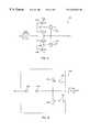
- an FPGA 46all input and output buffers share a common set of Vcc and ground power buses 48 and 50 .
- the input and/or output buffers of the mask programmable portion 14 of the present inventioncan either be connected to shared Vcc and ground power busses 52 and 54 and/or be segregated to certain Vcc and ground power bus portions 56 and 58 .
- the mask programmed portion 14can be used to substitute dedicated Vcc and ground power pads 60 and 62 for certain I/O locations, and thereby provide selected input and/or output buffers separate busses to I/O pins. Such an arrangement keeps the switching noise of a very high speed or high drive output from affecting other circuitry. It can also be used to isolate a very noise sensitive input from the switching noise of other circuits.
- the input and output buffers in the mask programmable portioncan be configured to respond to analog input signals.
- an input buffer 64 in the mask programmable portion 14is implemented as a comparator.
- the inputs to the input buffer 64are first and second analog input voltage, namely, V sense and V ref .
- the output of input buffer 64is a digital output that is supplied to the FPGA portion 12 of the integrated circuit 10 .
- an input buffer 66 having a multiplexer functionis implemented in the mask programmable portion 14 with a multiplexer 68 and an amplifier 70 .
- the inputs to the input buffer 66are a plurality of four analog input voltages.
- First and second select signals S 0 and S 1are provided to the multiplexer 68 by the FPGA portion.
- the analog output of the multiplexer 68is fed through an amplifier 70 to form the input buffer 66 output shown as being output off of the integrated circuit 10 .
- the analog signalmay also be fed into an analog circuit (not illustrated) formed in the mask programmable portion 14 of the integrated circuit 10 as disclosed in co-pending application Ser. No. 08/792,902, filed Jan.
- FIG. 4 aillustrates an input buffer 72 wherein the buffer is compatible with 74HC/AC technologies (“CMOS”).
- the input buffer 72comprises an inverter structure well known in the art having a P-channel MOS transistor 74 and an N-channel MOS transistor 76 .
- the conductivity of the P-channel MOS transistor 74is matched to the conductivity of the N-channel MOS transistor 76 such that the threshold voltage of the buffer, that is, the point at which V in is equal to V out , is set at V cc /2.
- FIG. 4 billustrates an input buffer 78 wherein the buffer is compatible with 74HCT/ACT/F/AS(“TTL”) technologies.
- input buffer 78is an inverter comprising P-channel MOS transistor 80 and N-channel MOS transistor 82 well known in the art to provide input level translation.
- the conductivity of the N-Channel MOS transistor 82is substantially greater than the conductivity of the P-Channel MOS transistor 80 .
- the conductivity in the N-Channel MOS transistor 82is greater than conductivity of the P-Channel MOS transistor 82 so that the point in input buffer 78 at which the V in is equal to V out is equal to a voltage of 1.4 volts. This value is obtained as an average of the lower TTL voltage of 0.8 volts and the upper TTL voltage of 2.0 volts.
- FIG. 4Cdepicts an input buffer 84 which can be programmed with a signal from the FPGA portion 12 of the integrated circuit 10 to respond to either of the input threshold voltages of input buffers 72 and 78 .
- a P-Channel MOS transistor 86 and an N-Channel MOS transistor 88correspond to the P-Channel MOS transistor 74 and the N-Channel MOS transistor 76 of input buffer 72 .
- an N-Channel MOS transistor 90has its drain connected to the output of the invertor represented by P-Channel MOS transistor 86 and N-Channel MOS transistor 88 and its source connected to the drain of an N-Channel MOS transistor 92 having its source connected to ground.
- the gate of N-Channel MOS transistor 92is connected to the input pad along with the gate of N-Channel MOS transistor 88 , and the gate of N-Channel MOS transistor 90 is connected to the signal controlled by the programmable element.
- the gate of N-channel MOS transistor 90can be mask programmed to be tied to either Vcc or ground.
- the N-Channel MOS transistor 90 and the N-Channel MOS transistor 92adjust the ratio of the conductivities of P-Channel MOS transistor 86 and N-Channel MOS transistor 88 to match the ratio of conductivities of the P-Channel MOS transistor 80 and N-Channel MOS transistor 82 in input buffer 78 . It should be appreciated by those of ordinary skill in the art, that input buffer thresholds other than those of input buffers 72 and 78 could be implemented by the input buffer 84 .
- the implementation of other input buffer thresholdsis made by placing an appropriate number of pairs of N-Channel MOS transistors in parallel with the N-Channel MOS transistors 90 and 92 , respectively, to compensate for the ratio of conductivities of P-Channel and N-Channel MOS transistors 86 and 88 .
- a Schmitt trigger 100is shown which may be implemented in the mask programmable portion 14 of the integrated circuit 10 on an as needed basis.
- Schmitt trigger 100the thresholds for rising edge and falling edge inputs are spread apart to create a deadband. This deadband resists unwanted oscillations caused by noise on very slow input edge rates.
- the size of the deadband in Schmitt trigger 100is varied by adjusting the ratio of conductivities between a first set of transistors comprising of P-Channel MOS transistors 102 and 104 , and N-Channel MOS transistors 106 and 108 , and a second group of transistors comprising N-Channel MOS transistor 110 and P-Channel MOS transistor 112 .
- inputs to the mask programmable portion 14 of the integrated circuitcan be varied to make the desired choice in the tradeoff between noise immunity and propagation delay.
- a standard input bufferwill typically be constructed of devices which are large enough to offer good switching speed, yet operate within a particular power (AC or DC) or area budget. A few important signals may require faster speed, which can be produced by an input buffer with larger devices.
- a noise or power sensitive designmay desire input buffers with very small sizes (reduced capacitance, reduced totem pole currents, etc.).
- these specialized input bufferscan be implemented in the mask programmable portion 14 of the integrated circuit 10 , while the standard buffers are implemented in the FPGA portion 12 of the integrated circuit 10 .
- FIG. 6illustrates an output buffer 120 for the mask programmable portion 14 of the integrated circuit 10 .
- Output buffer 120is a very efficient output buffer having a high DC drive. Switching in output buffer 120 is accomplished by first and second inverters 122 and 124 comprising MOS transistors as is well known in the art. The MOS transistors in first and second inverters 122 and 124 can be made small, and thereby produce limited totem-pole power dissipation. High output drive is provided by P-Channel and N-channel MOS transistors 126 and 128 which are relatively large devices. Power is limited because P-Channel and N-channel MOS transistors 126 and 128 are turned on by NAND gate 130 and NOR gate 132 , respectively, only after switching occurs and not both at the same time.
- a more common method of saving poweris to limit voltage swing at the output pad.
- the voltage swing at the outputmay be reduced by over 1 volt. Since power dissipation is proportional to the square of the output voltage swing, the reduction in power consumption can be substantial. It is advantageous to implement such structures in the mask programmable portion 14 , while implementing more general purpose full rail-to-rail swing buffers in the FPGA portion 12 .
- the voltage swing at the outputmay be further reduced by providing a lower Vcc.
- the speed in the output buffercan be enhanced by mask programming.
- a common example of thisis “clock-to-out” wherein the delay from a clocked flip-flop through an output buffer is critical.
- the speedmay be a problem because the flip-flop may not lie adjacent to the output buffer due to layout constraints and/or FPGA output buffers are usually general purpose that can support tri-state and other functions.
- the flip-flopIn the mask programmed portion the flip-flop can be placed adjacent to the output buffer for a more compact layout, and large area fast output buffer with no tri-state capability can be employed.
- output bufferssuch as the output buffers disclosed in application Ser. No. 08/673,701, filed Jun. 25, 1996, assigned to the same assignee as the present invention, and expressly incorporated herein by reference, wherein the output voltage may be connected to a mixed voltage levels system.
- the output voltagemay be connected to a mixed voltage levels system.
- a circuit designwhere only a few pins need mixed voltage capabilities (e.g., in a 3.3 volt design where a small number of pins need to interface to 5 volt levels)
- level shiftingcan be accomplished on an as needed basis in the mask programmed portion 14 . This permits the FPGA to have a more generic output buffer with smaller space, lower power, and faster propagation delay.
- the integrated circuit 10may be interfaced to an external voltage greater than V cc .
- the last stage in an FPGA output buffer 140 as illustrated in FIG. 7 ais typically an output totem pole stage comprising P-channel and N-channel MOS transistors 142 and 144 having inherent parasitic diodes 146 and 148 .
- the output buffer 140will typically clamp an output pad 150 at one diode voltage above V cc .
- N-channel MOS transistor 144is configured as an open drain structure, and the inherent parasitic diode 146 is open circuited.
- the output swingis limited to the breakdown voltages of the N-channel (or NPN) devices of the mask programmed portion 14 .
- NPNNPN
- With an external pull-up resistor 162it is conceivable that the output buffer 160 could control a 12 volt interface. This is not possible with the generic CMOS output buffer 140 .
- I/O buffer circuitsexist that may be implemented better in the mask programmable portion 14 of the integrated circuit 10 according to the present invention than in the FPGA portion 12 of the integrated circuit 10 .
- Examplesinclude but are not limited to metastable hardened inputs and low-voltage differential signaling input buffers.
Landscapes
- Physics & Mathematics (AREA)
- Mathematical Physics (AREA)
- Engineering & Computer Science (AREA)
- Computer Hardware Design (AREA)
- Computing Systems (AREA)
- General Engineering & Computer Science (AREA)
- Design And Manufacture Of Integrated Circuits (AREA)
Abstract
Description
Claims (21)
Priority Applications (1)
| Application Number | Priority Date | Filing Date | Title |
|---|---|---|---|
| US09/286,128US6362649B1 (en) | 1997-01-31 | 1999-04-02 | Field programmable gate array with mask programmed input and output buffers |
Applications Claiming Priority (2)
| Application Number | Priority Date | Filing Date | Title |
|---|---|---|---|
| US08/792,482US5959466A (en) | 1997-01-31 | 1997-01-31 | Field programmable gate array with mask programmed input and output buffers |
| US09/286,128US6362649B1 (en) | 1997-01-31 | 1999-04-02 | Field programmable gate array with mask programmed input and output buffers |
Related Parent Applications (1)
| Application Number | Title | Priority Date | Filing Date |
|---|---|---|---|
| US08/792,482ContinuationUS5959466A (en) | 1997-01-31 | 1997-01-31 | Field programmable gate array with mask programmed input and output buffers |
Publications (1)
| Publication Number | Publication Date |
|---|---|
| US6362649B1true US6362649B1 (en) | 2002-03-26 |
Family
ID=25157031
Family Applications (2)
| Application Number | Title | Priority Date | Filing Date |
|---|---|---|---|
| US08/792,482Expired - LifetimeUS5959466A (en) | 1997-01-31 | 1997-01-31 | Field programmable gate array with mask programmed input and output buffers |
| US09/286,128Expired - Fee RelatedUS6362649B1 (en) | 1997-01-31 | 1999-04-02 | Field programmable gate array with mask programmed input and output buffers |
Family Applications Before (1)
| Application Number | Title | Priority Date | Filing Date |
|---|---|---|---|
| US08/792,482Expired - LifetimeUS5959466A (en) | 1997-01-31 | 1997-01-31 | Field programmable gate array with mask programmed input and output buffers |
Country Status (1)
| Country | Link |
|---|---|
| US (2) | US5959466A (en) |
Cited By (15)
| Publication number | Priority date | Publication date | Assignee | Title |
|---|---|---|---|---|
| US6625672B1 (en)* | 1999-04-12 | 2003-09-23 | Telefonaktiebolaget Lm Ericsson (Publ) | Divided buffer |
| US20040174187A1 (en)* | 2003-03-03 | 2004-09-09 | Xilinx, Inc. | FPGA architecture with mixed interconnect resources optimized for fast and low-power routing and methods of utilizing the same |
| US20050235088A1 (en)* | 2004-04-20 | 2005-10-20 | Hynix Semiconductor Inc. | Multi-protocol serial interface system |
| US20050262461A1 (en)* | 2004-05-21 | 2005-11-24 | Hsin-Wo Fang | Input/output circuits with programmable option and related method |
| US20060020907A1 (en)* | 2004-07-23 | 2006-01-26 | Nec Electronics Corporation | Copy protection method and system for programmable gate array |
| US20060195645A1 (en)* | 2003-06-06 | 2006-08-31 | Stuart Ryan | Interface for prototyping integrated systems |
| US7243312B1 (en) | 2003-10-24 | 2007-07-10 | Xilinx, Inc. | Method and apparatus for power optimization during an integrated circuit design process |
| US7389485B1 (en) | 2006-03-28 | 2008-06-17 | Xilinx, Inc. | Methods of routing low-power designs in programmable logic devices having heterogeneous routing architectures |
| US20090174482A1 (en)* | 2006-04-26 | 2009-07-09 | Nxp B.V. | High power integrated rf amplifier |
| US7893712B1 (en) | 2009-09-10 | 2011-02-22 | Xilinx, Inc. | Integrated circuit with a selectable interconnect circuit for low power or high performance operation |
| US8179161B1 (en) | 2009-05-05 | 2012-05-15 | Cypress Semiconductor Corporation | Programmable input/output circuit |
| US8987868B1 (en) | 2009-02-24 | 2015-03-24 | Xilinx, Inc. | Method and apparatus for programmable heterogeneous integration of stacked semiconductor die |
| US9000490B2 (en) | 2013-04-19 | 2015-04-07 | Xilinx, Inc. | Semiconductor package having IC dice and voltage tuners |
| US9015023B2 (en) | 2010-05-05 | 2015-04-21 | Xilinx, Inc. | Device specific configuration of operating voltage |
| US9952282B1 (en) | 2009-05-05 | 2018-04-24 | Cypress Semiconductor Corporation | Combined analog architecture and functionality in a mixed-signal array |
Families Citing this family (25)
| Publication number | Priority date | Publication date | Assignee | Title |
|---|---|---|---|---|
| US5959466A (en)* | 1997-01-31 | 1999-09-28 | Actel Corporation | Field programmable gate array with mask programmed input and output buffers |
| US5874834A (en)* | 1997-03-04 | 1999-02-23 | Xilinx, Inc. | Field programmable gate array with distributed gate-array functionality |
| US7389487B1 (en)* | 1998-04-28 | 2008-06-17 | Actel Corporation | Dedicated interface architecture for a hybrid integrated circuit |
| US6163166A (en)* | 1998-05-27 | 2000-12-19 | Altera Corporation | Programmable logic device with selectable schmitt-triggered and threshold-triggered buffers |
| US6810042B1 (en)* | 1999-01-04 | 2004-10-26 | Cisco Technology, Inc. | Method of queuing traffic to many destinations covering a wide range of transmission speeds while minimizing buffer size |
| US6236229B1 (en) | 1999-05-13 | 2001-05-22 | Easic Corporation | Integrated circuits which employ look up tables to provide highly efficient logic cells and logic functionalities |
| US6194912B1 (en)* | 1999-03-11 | 2001-02-27 | Easic Corporation | Integrated circuit device |
| US6331733B1 (en) | 1999-08-10 | 2001-12-18 | Easic Corporation | Semiconductor device |
| US6245634B1 (en) | 1999-10-28 | 2001-06-12 | Easic Corporation | Method for design and manufacture of semiconductors |
| US6172518B1 (en)* | 1999-07-23 | 2001-01-09 | Xilinx, Inc. | Method of minimizing power use in programmable logic devices |
| US6346427B1 (en) | 1999-08-18 | 2002-02-12 | Utmc Microelectronic Systems Inc. | Parameter adjustment in a MOS integrated circuit |
| US6331790B1 (en) | 2000-03-10 | 2001-12-18 | Easic Corporation | Customizable and programmable cell array |
| US6756811B2 (en)* | 2000-03-10 | 2004-06-29 | Easic Corporation | Customizable and programmable cell array |
| US7024653B1 (en)* | 2000-10-30 | 2006-04-04 | Cypress Semiconductor Corporation | Architecture for efficient implementation of serial data communication functions on a programmable logic device (PLD) |
| US6895570B2 (en) | 2001-05-06 | 2005-05-17 | Altera Corporation | System and method for optimizing routing lines in a programmable logic device |
| SE0102199D0 (en)* | 2001-06-20 | 2001-06-20 | Ericsson Telefon Ab L M | Upgrading field programmable gate arrays over data communication networks |
| US7112994B2 (en) | 2002-07-08 | 2006-09-26 | Viciciv Technology | Three dimensional integrated circuits |
| US6992503B2 (en) | 2002-07-08 | 2006-01-31 | Viciciv Technology | Programmable devices with convertibility to customizable devices |
| US8643162B2 (en) | 2007-11-19 | 2014-02-04 | Raminda Udaya Madurawe | Pads and pin-outs in three dimensional integrated circuits |
| US7095063B2 (en)* | 2003-05-07 | 2006-08-22 | International Business Machines Corporation | Multiple supply gate array backfill structure |
| US7030651B2 (en) | 2003-12-04 | 2006-04-18 | Viciciv Technology | Programmable structured arrays |
| US7064580B2 (en)* | 2004-07-22 | 2006-06-20 | Altera Corporation | Mask-programmable logic device with programmable portions |
| DE102010033780A1 (en)* | 2010-08-09 | 2012-02-09 | Volkswagen Ag | Integrated circuit unit e.g. field-programmable gate array, for generating output signal utilized for controlling e.g. MOSFET of electromotor in motor car, has external pull-up resistor setting output current strength |
| US9742585B2 (en) | 2014-11-20 | 2017-08-22 | Lenovo Enterprise Solutions (Singapore) Pte. Ltd. | Signaling control among multiple communication interfaces of an electronic device based on signal priority |
| US10003338B2 (en)* | 2016-07-21 | 2018-06-19 | Andapt, Inc. | Programmable analog and digital input/output for power application |
Citations (157)
| Publication number | Priority date | Publication date | Assignee | Title |
|---|---|---|---|---|
| US4195352A (en) | 1977-07-08 | 1980-03-25 | Xerox Corporation | Split programmable logic array |
| GB2045488B (en) | 1979-01-16 | 1982-10-13 | Nippon Telegraph & Telephone | Programmable sequential logic circuit devices |
| US4458163A (en) | 1981-07-20 | 1984-07-03 | Texas Instruments Incorporated | Programmable architecture logic |
| US4527115A (en) | 1982-12-22 | 1985-07-02 | Raytheon Company | Configurable logic gate array |
| EP0081917B1 (en) | 1981-11-18 | 1986-06-11 | BURROUGHS CORPORATION (a Delaware corporation) | Programmable multiplexer |
| US4609986A (en) | 1984-06-14 | 1986-09-02 | Altera Corporation | Programmable logic array device using EPROM technology |
| US4631686A (en) | 1983-08-31 | 1986-12-23 | Kabushiki Kaisha Toshiba | Semiconductor integrated circuit device |
| US4677318A (en) | 1985-04-12 | 1987-06-30 | Altera Corporation | Programmable logic storage element for programmable logic devices |
| US4684830A (en) | 1985-03-22 | 1987-08-04 | Monolithic Memories, Inc. | Output circuit for a programmable logic array |
| US4691161A (en) | 1985-06-13 | 1987-09-01 | Raytheon Company | Configurable logic gate array |
| US4713792A (en) | 1985-06-06 | 1987-12-15 | Altera Corporation | Programmable macrocell using eprom or eeprom transistors for architecture control in programmable logic circuits |
| US4718057A (en) | 1985-08-30 | 1988-01-05 | Advanced Micro Devices, Inc. | Streamlined digital signal processor |
| US4721868A (en) | 1986-09-23 | 1988-01-26 | Advanced Micro Devices, Inc. | IC input circuitry programmable for realizing multiple functions from a single input |
| US4758747A (en) | 1986-05-30 | 1988-07-19 | Advanced Micro Devices, Inc. | Programmable logic device with buried registers selectively multiplexed with output registers to ports, and preload circuitry therefor |
| US4771285A (en) | 1985-11-05 | 1988-09-13 | Advanced Micro Devices, Inc. | Programmable logic cell with flexible clocking and flexible feedback |
| US4772811A (en) | 1986-07-04 | 1988-09-20 | Ricoh Company, Ltd. | Programmable logic device |
| US4774421A (en) | 1984-05-03 | 1988-09-27 | Altera Corporation | Programmable logic array device using EPROM technology |
| US4783606A (en) | 1987-04-14 | 1988-11-08 | Erich Goetting | Programming circuit for programmable logic array I/O cell |
| EP0069762B1 (en) | 1981-01-16 | 1989-02-08 | JOHNSON, Robert Royce | Universal interconnection substrate |
| US4847612A (en) | 1988-01-13 | 1989-07-11 | Plug Logic, Inc. | Programmable logic device |
| US4857774A (en) | 1986-09-19 | 1989-08-15 | Actel Corporation | Testing apparatus and diagnostic method for use with programmable interconnect architecture |
| EP0358501A2 (en) | 1988-09-08 | 1990-03-14 | Kawasaki Steel Corporation | Programmable input/output circuit |
| US4910466A (en) | 1985-12-20 | 1990-03-20 | Hitachi Microcomputer Engineering Ltd. | Selecting means for selecting a plurality of information |
| US4912345A (en) | 1988-12-29 | 1990-03-27 | Sgs-Thomson Microelectronics, Inc. | Programmable summing functions for programmable logic devices |
| US4931671A (en) | 1985-03-29 | 1990-06-05 | Advanced Micro Devices, Inc. | Multiple array customizable logic device |
| US4933577A (en) | 1985-03-22 | 1990-06-12 | Advanced Micro Devices, Inc. | Output circuit for a programmable logic array |
| US4933898A (en) | 1989-01-12 | 1990-06-12 | General Instrument Corporation | Secure integrated circuit chip with conductive shield |
| US4940909A (en) | 1989-05-12 | 1990-07-10 | Plus Logic, Inc. | Configuration control circuit for programmable logic devices |
| US4952934A (en) | 1989-01-25 | 1990-08-28 | Sgs-Thomson Microelectronics S.R.L. | Field programmable logic and analogic integrated circuit |
| US4963768A (en) | 1985-03-29 | 1990-10-16 | Advanced Micro Devices, Inc. | Flexible, programmable cell array interconnected by a programmable switch matrix |
| US4969121A (en) | 1987-03-02 | 1990-11-06 | Altera Corporation | Programmable integrated circuit logic array device having improved microprocessor connectability |
| US4983959A (en) | 1986-10-01 | 1991-01-08 | Texas Instruments Incorporated | Logic output macrocell |
| US4992680A (en) | 1988-12-28 | 1991-02-12 | Sgs-Thomson Microelectronics S.R.L. | Programmable logic device having a plurality of programmable logic arrays arranged in a mosaic layout together with a plurality of interminglingly arranged interfacing blocks |
| US5023484A (en) | 1988-09-02 | 1991-06-11 | Cypress Semiconductor Corporation | Architecture of high speed synchronous state machine |
| US5027011A (en) | 1989-10-31 | 1991-06-25 | Sgs-Thomson Microelectronics, Inc. | Input row drivers for programmable logic devices |
| US5028821A (en) | 1990-03-01 | 1991-07-02 | Plus Logic, Inc. | Programmable logic device with programmable inverters at input/output pads |
| US5045726A (en) | 1990-05-16 | 1991-09-03 | North American Philips Corporation | Low power programming circuit for user programmable digital logic array |
| EP0415542A3 (en) | 1989-08-15 | 1991-10-02 | Advanced Micro Devices, Inc. | Programmable gate array with improved interconnect structure, input/output structure and configurable logic block |
| US5068603A (en) | 1987-10-07 | 1991-11-26 | Xilinx, Inc. | Structure and method for producing mask-programmed integrated circuits which are pin compatible substitutes for memory-configured logic arrays |
| US5083293A (en) | 1989-01-12 | 1992-01-21 | General Instrument Corporation | Prevention of alteration of data stored in secure integrated circuit chip memory |
| US5107146A (en) | 1991-02-13 | 1992-04-21 | Actel Corporation | Mixed mode analog/digital programmable interconnect architecture |
| US5140193A (en) | 1990-03-27 | 1992-08-18 | Xilinx, Inc. | Programmable connector for programmable logic device |
| US5151623A (en) | 1985-03-29 | 1992-09-29 | Advanced Micro Devices, Inc. | Programmable logic device with multiple, flexible asynchronous programmable logic blocks interconnected by a high speed switch matrix |
| US5153462A (en) | 1991-05-21 | 1992-10-06 | Advanced Micro Devices, Inc. | Programmable logic device incorporating voltage comparator |
| US5166557A (en) | 1991-01-02 | 1992-11-24 | Texas Instruments Incorporated | Gate array with built-in programming circuitry |
| US5191242A (en) | 1991-05-17 | 1993-03-02 | Advanced Micro Devices, Inc. | Programmable logic device incorporating digital-to-analog converter |
| US5220213A (en) | 1991-03-06 | 1993-06-15 | Quicklogic Corporation | Programmable application specific integrated circuit and logic cell therefor |
| US5221865A (en) | 1991-06-21 | 1993-06-22 | Crosspoint Solutions, Inc. | Programmable input/output buffer circuit with test capability |
| US5225719A (en) | 1985-03-29 | 1993-07-06 | Advanced Micro Devices, Inc. | Family of multiple segmented programmable logic blocks interconnected by a high speed centralized switch matrix |
| US5231588A (en) | 1989-08-15 | 1993-07-27 | Advanced Micro Devices, Inc. | Programmable gate array with logic cells having symmetrical input/output structures |
| US5258891A (en) | 1990-11-29 | 1993-11-02 | Kawasaki Steel Corporation | Multichip module with multilayer wiring substrate |
| US5301143A (en) | 1992-12-31 | 1994-04-05 | Micron Semiconductor, Inc. | Method for identifying a semiconductor die using an IC with programmable links |
| US5311080A (en) | 1993-03-26 | 1994-05-10 | At&T Bell Laboratories | Field programmable gate array with direct input/output connection |
| US5313119A (en) | 1991-03-18 | 1994-05-17 | Crosspoint Solutions, Inc. | Field programmable gate array |
| US5317698A (en) | 1992-08-18 | 1994-05-31 | Actel Corporation | FPGA architecture including direct logic function circuit to I/O interconnections |
| US5317212A (en) | 1993-03-19 | 1994-05-31 | Wahlstrom Sven E | Dynamic control of configurable logic |
| US5323069A (en) | 1991-08-29 | 1994-06-21 | National Semiconductor Corporation | Direct I/O access to express bussing in a configurable logic array |
| US5329181A (en) | 1993-03-05 | 1994-07-12 | Xilinx, Inc. | Complementary macrocell feedback circuit |
| US5343406A (en) | 1989-07-28 | 1994-08-30 | Xilinx, Inc. | Distributed memory architecture for a configurable logic array and method for using distributed memory |
| US5349249A (en) | 1993-04-07 | 1994-09-20 | Xilinx, Inc. | Programmable logic device having security elements located amongst configuration bit location to prevent unauthorized reading |
| US5357153A (en) | 1993-01-28 | 1994-10-18 | Xilinx, Inc. | Macrocell with product-term cascade and improved flip flop utilization |
| EP0592111A3 (en) | 1992-10-08 | 1994-12-21 | Aptix Corp | Multichip module for integrated semiconductor components with a maximum of input and output options. |
| US5377124A (en) | 1989-09-20 | 1994-12-27 | Aptix Corporation | Field programmable printed circuit board |
| US5381058A (en) | 1993-05-21 | 1995-01-10 | At&T Corp. | FPGA having PFU with programmable output driver inputs |
| US5394031A (en) | 1993-12-08 | 1995-02-28 | At&T Corp. | Apparatus and method to improve programming speed of field programmable gate arrays |
| US5402014A (en) | 1993-07-14 | 1995-03-28 | Waferscale Integration, Inc. | Peripheral port with volatile and non-volatile configuration |
| US5404033A (en) | 1992-08-20 | 1995-04-04 | Swift Microelectronics Corporation | Application specific integrated circuit and placement and routing software with non-customizable first metal layer and vias and customizable second metal grid pattern |
| US5414638A (en) | 1992-12-18 | 1995-05-09 | Aptix Corporation | Programmable interconnect architecture |
| US5424589A (en) | 1993-02-12 | 1995-06-13 | The Board Of Trustees Of The Leland Stanford Junior University | Electrically programmable inter-chip interconnect architecture |
| US5424655A (en) | 1994-05-20 | 1995-06-13 | Quicklogic Corporation | Programmable application specific integrated circuit employing antifuses and methods therefor |
| US5426378A (en) | 1994-04-20 | 1995-06-20 | Xilinx, Inc. | Programmable logic device which stores more than one configuration and means for switching configurations |
| US5426379A (en) | 1994-07-29 | 1995-06-20 | Xilinx, Inc. | Field programmable gate array with built-in bitstream data expansion |
| US5438166A (en) | 1987-09-29 | 1995-08-01 | Microelectronics And Computer Technology Corporation | Customizable circuitry |
| US5440453A (en) | 1991-12-18 | 1995-08-08 | Crosspoint Solutions, Inc. | Extended architecture for FPGA |
| US5444394A (en) | 1993-07-08 | 1995-08-22 | Altera Corporation | PLD with selective inputs from local and global conductors |
| US5448493A (en) | 1989-12-20 | 1995-09-05 | Xilinx, Inc. | Structure and method for manually controlling automatic configuration in an integrated circuit logic block array |
| US5452229A (en) | 1992-12-18 | 1995-09-19 | Lattice Semiconductor Corporation | Programmable integrated-circuit switch |
| US5457409A (en) | 1992-08-03 | 1995-10-10 | Advanced Micro Devices, Inc. | Architecture of a multiple array high density programmable logic device with a plurality of programmable switch matrices |
| US5457410A (en) | 1993-08-03 | 1995-10-10 | Btr, Inc. | Architecture and interconnect scheme for programmable logic circuits |
| US5457644A (en) | 1993-08-20 | 1995-10-10 | Actel Corporation | Field programmable digital signal processing array integrated circuit |
| US5469003A (en) | 1992-11-05 | 1995-11-21 | Xilinx, Inc. | Hierarchically connectable configurable cellular array |
| US5488317A (en) | 1993-10-22 | 1996-01-30 | Texas Instruments Incorporated | Wired logic functions on FPGA's |
| US5490042A (en) | 1992-08-10 | 1996-02-06 | Environmental Research Institute Of Michigan | Programmable silicon circuit board |
| US5493239A (en) | 1995-01-31 | 1996-02-20 | Motorola, Inc. | Circuit and method of configuring a field programmable gate array |
| US5498886A (en) | 1991-11-05 | 1996-03-12 | Monolithic System Technology, Inc. | Circuit module redundancy architecture |
| US5504354A (en) | 1990-10-15 | 1996-04-02 | Aptix Corporation | Interconnect substrate with circuits for field-programmability and testing of multichip modules and hybrid circuits |
| US5504439A (en) | 1994-04-01 | 1996-04-02 | Xilinx, Inc. | I/O interface cell for use with optional pad |
| US5521529A (en) | 1995-06-02 | 1996-05-28 | Advanced Micro Devices, Inc. | Very high-density complex programmable logic devices with a multi-tiered hierarchical switch matrix and optimized flexible logic allocation |
| US5530378A (en) | 1995-04-26 | 1996-06-25 | Xilinx, Inc. | Cross point interconnect structure with reduced area |
| US5537341A (en) | 1995-02-10 | 1996-07-16 | Jonathan Rose | Complementary architecture for field-programmable gate arrays |
| US5539692A (en) | 1993-02-19 | 1996-07-23 | Hitachi, Ltd. | Semiconductor memory and method of setting type |
| US5543730A (en) | 1995-05-17 | 1996-08-06 | Altera Corporation | Techniques for programming programmable logic array devices |
| US5548552A (en) | 1994-09-28 | 1996-08-20 | Altera Corporation | Reconfigurable programmable logic device |
| US5550839A (en) | 1993-03-12 | 1996-08-27 | Xilinx, Inc. | Mask-programmed integrated circuits having timing and logic compatibility to user-configured logic arrays |
| EP0584910B1 (en) | 1992-08-03 | 1996-09-04 | Advanced Micro Devices, Inc. | Programmable logic device |
| US5559465A (en) | 1994-07-29 | 1996-09-24 | Cypress Semiconductor Corporation | Output preconditioning circuit with an output level latch and a clamp |
| US5559447A (en) | 1994-11-17 | 1996-09-24 | Cypress Semiconductor | Output buffer with variable output impedance |
| US5563528A (en) | 1995-05-02 | 1996-10-08 | Xilinx, Inc. | Multiplexer for programmable logic device |
| US5563526A (en) | 1994-01-03 | 1996-10-08 | Texas Instruments Incorporated | Programmable mixed-mode integrated circuit architecture |
| US5563592A (en) | 1993-11-22 | 1996-10-08 | Altera Corporation | Programmable logic device having a compressed configuration file and associated decompression |
| US5565793A (en) | 1995-08-22 | 1996-10-15 | Altera Corporation | Programmable logic array integrated circuit devices with regions of enhanced interconnectivity |
| US5568081A (en) | 1995-06-07 | 1996-10-22 | Cypress Semiconductor, Corporation | Variable slew control for output buffers |
| US5570040A (en) | 1995-03-22 | 1996-10-29 | Altera Corporation | Programmable logic array integrated circuit incorporating a first-in first-out memory |
| US5572148A (en) | 1995-03-22 | 1996-11-05 | Altera Corporation | Programmable logic array integrated circuit with general-purpose memory configurable as a random access or FIFO memory |
| US5572409A (en) | 1994-02-08 | 1996-11-05 | Prolinx Labs Corporation | Apparatus including a programmable socket adapter for coupling an electronic component to a component socket on a printed circuit board |
| US5576554A (en) | 1991-11-05 | 1996-11-19 | Monolithic System Technology, Inc. | Wafer-scale integrated circuit interconnect structure architecture |
| US5577050A (en) | 1994-12-28 | 1996-11-19 | Lsi Logic Corporation | Method and apparatus for configurable build-in self-repairing of ASIC memories design |
| US5581501A (en) | 1995-08-17 | 1996-12-03 | Altera Corporation | Nonvolatile SRAM cells and cell arrays |
| US5581198A (en) | 1995-02-24 | 1996-12-03 | Xilinx, Inc. | Shadow DRAM for programmable logic devices |
| US5583749A (en) | 1994-11-30 | 1996-12-10 | Altera Corporation | Baseboard and daughtercard apparatus for reconfigurable computing systems |
| US5583452A (en) | 1995-10-26 | 1996-12-10 | Xilinx, Inc. | Tri-directional buffer |
| US5583450A (en) | 1995-08-18 | 1996-12-10 | Xilinx, Inc. | Sequencer for a time multiplexed programmable logic device |
| US5587669A (en) | 1991-03-06 | 1996-12-24 | Quicklogic Corporation | Programmable application specific integrated circuit and logic cell therefor |
| US5590305A (en) | 1994-03-28 | 1996-12-31 | Altera Corporation | Programming circuits and techniques for programming logic |
| US5592509A (en) | 1994-04-15 | 1997-01-07 | Texas Instruments | Transceiver circuit with transition detection |
| US5592632A (en) | 1991-11-05 | 1997-01-07 | Monolithic System Technology, Inc. | Defect tolerant integrated circuit subsystem for communication between a module and a bus controller in a wafer-scale integrated circuit system |
| US5594690A (en) | 1995-12-15 | 1997-01-14 | Unisys Corporation | Integrated circuit memory having high speed and low power by selectively coupling compensation components to a pulse generator |
| US5594367A (en) | 1995-10-16 | 1997-01-14 | Xilinx, Inc. | Output multiplexer within input/output circuit for time multiplexing and high speed logic |
| US5598108A (en)* | 1991-04-25 | 1997-01-28 | Altera Corporation | High-density erasable programmable logic device architecture using multiplexer interconnections, and registered macrocell with product term allocation and adjacent product term stealing |
| US5600264A (en) | 1995-10-16 | 1997-02-04 | Xilinx, Inc. | Programmable single buffered six pass transistor configuration |
| US5600263A (en) | 1995-08-18 | 1997-02-04 | Xilinx, Inc. | Configuration modes for a time multiplexed programmable logic device |
| US5600267A (en) | 1994-06-24 | 1997-02-04 | Cypress Semiconductor Corporation | Apparatus for a programmable CML to CMOS translator for power/speed adjustment |
| US5600597A (en) | 1995-05-02 | 1997-02-04 | Xilinx, Inc. | Register protection structure for FPGA |
| US5625301A (en)* | 1995-05-18 | 1997-04-29 | Actel Corporation | Flexible FPGA input/output architecture |
| US5631577A (en) | 1995-02-10 | 1997-05-20 | Xilinx, Inc. | Synchronous dual port RAM |
| US5633830A (en) | 1995-11-08 | 1997-05-27 | Altera Corporation | Random access memory block circuitry for programmable logic array integrated circuit devices |
| US5635851A (en) | 1996-02-02 | 1997-06-03 | Xilinx, Inc. | Read and writable data bus particularly for programmable logic devices |
| US5640308A (en) | 1991-06-14 | 1997-06-17 | Aptix Corporation | Field programmable circuit module |
| US5640106A (en) | 1995-05-26 | 1997-06-17 | Xilinx, Inc. | Method and structure for loading data into several IC devices |
| US5642058A (en) | 1995-10-16 | 1997-06-24 | Xilinx , Inc. | Periphery input/output interconnect structure |
| US5642262A (en) | 1995-02-23 | 1997-06-24 | Altera Corporation | High-density programmable logic device in a multi-chip module package with improved interconnect scheme |
| US5644496A (en) | 1989-08-15 | 1997-07-01 | Advanced Micro Devices, Inc. | Programmable logic device with internal time-constant multiplexing of signals from external interconnect buses |
| US5646544A (en) | 1995-06-05 | 1997-07-08 | International Business Machines Corporation | System and method for dynamically reconfiguring a programmable gate array |
| US5650734A (en) | 1995-12-11 | 1997-07-22 | Altera Corporation | Programming programmable transistor devices using state machines |
| US5652529A (en) | 1995-06-02 | 1997-07-29 | International Business Machines Corporation | Programmable array clock/reset resource |
| US5652904A (en) | 1993-08-03 | 1997-07-29 | Xilinx, Inc. | Non-reconfigurable microprocessor-emulated FPGA |
| US5661685A (en) | 1995-09-25 | 1997-08-26 | Xilinx, Inc. | Programmable logic device with configurable power supply |
| US5671432A (en) | 1995-06-02 | 1997-09-23 | International Business Machines Corporation | Programmable array I/O-routing resource |
| EP0585119B1 (en) | 1992-08-27 | 1997-10-22 | NCR International, Inc. | Programmable logic device |
| EP0583872B1 (en) | 1992-08-03 | 1997-10-29 | Advanced Micro Devices, Inc. | Flexible synchronous/asynchronous cell structure for a programmable logic device |
| EP0759662A3 (en) | 1995-08-18 | 1998-01-28 | Xilinx, Inc. | Time multiplexed programmable logic device |
| EP0785630A3 (en) | 1996-01-17 | 1998-04-15 | Hewlett-Packard Company | Time multiplexing in field programmable gate arrays |
| US5744979A (en) | 1992-07-23 | 1998-04-28 | Xilinx, Inc. | FPGA having logic cells configured by SRAM memory cells and interconnect configured by antifuses |
| US5744980A (en) | 1996-02-16 | 1998-04-28 | Actel Corporation | Flexible, high-performance static RAM architecture for field-programmable gate arrays |
| US5744981A (en) | 1994-01-27 | 1998-04-28 | Dyna Logic Corporation | Programmable logic cell with input polarity control |
| US5748009A (en) | 1995-06-02 | 1998-05-05 | International Business Machines Corporation | Programmable logic cell |
| US5751162A (en) | 1995-04-06 | 1998-05-12 | Texas Instruments Incorporated | Field programmable gate array logic module configurable as combinational or sequential circuits |
| US5760607A (en) | 1995-07-10 | 1998-06-02 | Xilinx, Inc. | System comprising field programmable gate array and intelligent memory |
| EP0612154B1 (en) | 1993-02-16 | 1998-07-01 | STMicroelectronics Limited | Programmable logic circuit |
| US5821776A (en)* | 1997-01-31 | 1998-10-13 | Actel Corporation | Field programmable gate array with mask programmed analog function circuits |
| EP0790706A3 (en) | 1996-02-14 | 1999-01-07 | Hewlett-Packard Company | Memory system |
| EP0780846A3 (en) | 1995-12-20 | 1999-07-14 | International Business Machines Corporation | Field programmable memory array |
| EP0818891A3 (en) | 1996-07-13 | 1999-08-18 | Mitel Semiconductor Limited | Programmable logic arrays |
| US5959466A (en)* | 1997-01-31 | 1999-09-28 | Actel Corporation | Field programmable gate array with mask programmed input and output buffers |
| EP0756383A3 (en) | 1995-07-27 | 2000-11-15 | AT&T IPM Corp. | Field programmable gate array with multi-port RAM |
| EP0896836B1 (en) | 1997-08-13 | 2001-09-05 | Firma Carl Freudenberg | Printing device for coating a sheet material with a paste |
| EP0786871B1 (en) | 1991-09-03 | 2001-12-19 | Altera Corporation (a Delaware Corporation) | Programmable logic array integrated circuits |
Family Cites Families (1)
| Publication number | Priority date | Publication date | Assignee | Title |
|---|---|---|---|---|
| US5687325A (en) | 1996-04-19 | 1997-11-11 | Chang; Web | Application specific field programmable gate array |
- 1997
- 1997-01-31USUS08/792,482patent/US5959466A/ennot_activeExpired - Lifetime
- 1999
- 1999-04-02USUS09/286,128patent/US6362649B1/ennot_activeExpired - Fee Related
Patent Citations (186)
| Publication number | Priority date | Publication date | Assignee | Title |
|---|---|---|---|---|
| US4195352A (en) | 1977-07-08 | 1980-03-25 | Xerox Corporation | Split programmable logic array |
| GB2045488B (en) | 1979-01-16 | 1982-10-13 | Nippon Telegraph & Telephone | Programmable sequential logic circuit devices |
| EP0069762B1 (en) | 1981-01-16 | 1989-02-08 | JOHNSON, Robert Royce | Universal interconnection substrate |
| US4458163A (en) | 1981-07-20 | 1984-07-03 | Texas Instruments Incorporated | Programmable architecture logic |
| EP0081917B1 (en) | 1981-11-18 | 1986-06-11 | BURROUGHS CORPORATION (a Delaware corporation) | Programmable multiplexer |
| US4527115A (en) | 1982-12-22 | 1985-07-02 | Raytheon Company | Configurable logic gate array |
| US4631686A (en) | 1983-08-31 | 1986-12-23 | Kabushiki Kaisha Toshiba | Semiconductor integrated circuit device |
| US4774421A (en) | 1984-05-03 | 1988-09-27 | Altera Corporation | Programmable logic array device using EPROM technology |
| US4609986A (en) | 1984-06-14 | 1986-09-02 | Altera Corporation | Programmable logic array device using EPROM technology |
| US4684830A (en) | 1985-03-22 | 1987-08-04 | Monolithic Memories, Inc. | Output circuit for a programmable logic array |
| US4933577A (en) | 1985-03-22 | 1990-06-12 | Advanced Micro Devices, Inc. | Output circuit for a programmable logic array |
| US5225719A (en) | 1985-03-29 | 1993-07-06 | Advanced Micro Devices, Inc. | Family of multiple segmented programmable logic blocks interconnected by a high speed centralized switch matrix |
| US4931671A (en) | 1985-03-29 | 1990-06-05 | Advanced Micro Devices, Inc. | Multiple array customizable logic device |
| US5426335A (en) | 1985-03-29 | 1995-06-20 | Advanced Micro Devices, Inc. | Pinout architecture for a family of multiple segmented programmable logic blocks interconnected by a high speed centralized switch matrix |
| US4963768A (en) | 1985-03-29 | 1990-10-16 | Advanced Micro Devices, Inc. | Flexible, programmable cell array interconnected by a programmable switch matrix |
| US5485104A (en) | 1985-03-29 | 1996-01-16 | Advanced Micro Devices, Inc. | Logic allocator for a programmable logic device |
| US5151623A (en) | 1985-03-29 | 1992-09-29 | Advanced Micro Devices, Inc. | Programmable logic device with multiple, flexible asynchronous programmable logic blocks interconnected by a high speed switch matrix |
| US4677318A (en) | 1985-04-12 | 1987-06-30 | Altera Corporation | Programmable logic storage element for programmable logic devices |
| US4713792A (en) | 1985-06-06 | 1987-12-15 | Altera Corporation | Programmable macrocell using eprom or eeprom transistors for architecture control in programmable logic circuits |
| US4691161A (en) | 1985-06-13 | 1987-09-01 | Raytheon Company | Configurable logic gate array |
| US4718057A (en) | 1985-08-30 | 1988-01-05 | Advanced Micro Devices, Inc. | Streamlined digital signal processor |
| US4771285A (en) | 1985-11-05 | 1988-09-13 | Advanced Micro Devices, Inc. | Programmable logic cell with flexible clocking and flexible feedback |
| US4910466A (en) | 1985-12-20 | 1990-03-20 | Hitachi Microcomputer Engineering Ltd. | Selecting means for selecting a plurality of information |
| US4758747A (en) | 1986-05-30 | 1988-07-19 | Advanced Micro Devices, Inc. | Programmable logic device with buried registers selectively multiplexed with output registers to ports, and preload circuitry therefor |
| US4772811A (en) | 1986-07-04 | 1988-09-20 | Ricoh Company, Ltd. | Programmable logic device |
| US4857774A (en) | 1986-09-19 | 1989-08-15 | Actel Corporation | Testing apparatus and diagnostic method for use with programmable interconnect architecture |
| US4721868A (en) | 1986-09-23 | 1988-01-26 | Advanced Micro Devices, Inc. | IC input circuitry programmable for realizing multiple functions from a single input |
| US4983959A (en) | 1986-10-01 | 1991-01-08 | Texas Instruments Incorporated | Logic output macrocell |
| US4969121A (en) | 1987-03-02 | 1990-11-06 | Altera Corporation | Programmable integrated circuit logic array device having improved microprocessor connectability |
| US4783606A (en) | 1987-04-14 | 1988-11-08 | Erich Goetting | Programming circuit for programmable logic array I/O cell |
| US5438166A (en) | 1987-09-29 | 1995-08-01 | Microelectronics And Computer Technology Corporation | Customizable circuitry |
| US5068603A (en) | 1987-10-07 | 1991-11-26 | Xilinx, Inc. | Structure and method for producing mask-programmed integrated circuits which are pin compatible substitutes for memory-configured logic arrays |
| US4847612A (en) | 1988-01-13 | 1989-07-11 | Plug Logic, Inc. | Programmable logic device |
| EP0394575B1 (en) | 1988-01-13 | 1995-08-16 | Xilinx, Inc. | Programmable logic device |
| US5023484A (en) | 1988-09-02 | 1991-06-11 | Cypress Semiconductor Corporation | Architecture of high speed synchronous state machine |
| EP0358501A2 (en) | 1988-09-08 | 1990-03-14 | Kawasaki Steel Corporation | Programmable input/output circuit |
| US4992680A (en) | 1988-12-28 | 1991-02-12 | Sgs-Thomson Microelectronics S.R.L. | Programmable logic device having a plurality of programmable logic arrays arranged in a mosaic layout together with a plurality of interminglingly arranged interfacing blocks |
| US4912345A (en) | 1988-12-29 | 1990-03-27 | Sgs-Thomson Microelectronics, Inc. | Programmable summing functions for programmable logic devices |
| US5083293A (en) | 1989-01-12 | 1992-01-21 | General Instrument Corporation | Prevention of alteration of data stored in secure integrated circuit chip memory |
| US4933898A (en) | 1989-01-12 | 1990-06-12 | General Instrument Corporation | Secure integrated circuit chip with conductive shield |
| US4952934A (en) | 1989-01-25 | 1990-08-28 | Sgs-Thomson Microelectronics S.R.L. | Field programmable logic and analogic integrated circuit |
| US4940909A (en) | 1989-05-12 | 1990-07-10 | Plus Logic, Inc. | Configuration control circuit for programmable logic devices |
| US5343406A (en) | 1989-07-28 | 1994-08-30 | Xilinx, Inc. | Distributed memory architecture for a configurable logic array and method for using distributed memory |
| US5644496A (en) | 1989-08-15 | 1997-07-01 | Advanced Micro Devices, Inc. | Programmable logic device with internal time-constant multiplexing of signals from external interconnect buses |
| US5231588A (en) | 1989-08-15 | 1993-07-27 | Advanced Micro Devices, Inc. | Programmable gate array with logic cells having symmetrical input/output structures |
| EP0415542A3 (en) | 1989-08-15 | 1991-10-02 | Advanced Micro Devices, Inc. | Programmable gate array with improved interconnect structure, input/output structure and configurable logic block |
| US5544069A (en) | 1989-09-20 | 1996-08-06 | Aptix Corporation | Structure having different levels of programmable integrated circuits interconnected through bus lines for interconnecting electronic components |
| US5377124A (en) | 1989-09-20 | 1994-12-27 | Aptix Corporation | Field programmable printed circuit board |
| US5661409A (en) | 1989-09-20 | 1997-08-26 | Aptix Corporation | Field programmable printed circuit board |
| US5027011A (en) | 1989-10-31 | 1991-06-25 | Sgs-Thomson Microelectronics, Inc. | Input row drivers for programmable logic devices |
| US5448493A (en) | 1989-12-20 | 1995-09-05 | Xilinx, Inc. | Structure and method for manually controlling automatic configuration in an integrated circuit logic block array |
| US5028821A (en) | 1990-03-01 | 1991-07-02 | Plus Logic, Inc. | Programmable logic device with programmable inverters at input/output pads |
| US5140193A (en) | 1990-03-27 | 1992-08-18 | Xilinx, Inc. | Programmable connector for programmable logic device |
| US5045726A (en) | 1990-05-16 | 1991-09-03 | North American Philips Corporation | Low power programming circuit for user programmable digital logic array |
| US5654564A (en) | 1990-10-15 | 1997-08-05 | Aptix Corporation | Interconnect structure with programmable IC for interconnecting electronic components, including circuitry for controlling programmable IC |
| US5504354A (en) | 1990-10-15 | 1996-04-02 | Aptix Corporation | Interconnect substrate with circuits for field-programmability and testing of multichip modules and hybrid circuits |
| US5258891A (en) | 1990-11-29 | 1993-11-02 | Kawasaki Steel Corporation | Multichip module with multilayer wiring substrate |
| US5166557A (en) | 1991-01-02 | 1992-11-24 | Texas Instruments Incorporated | Gate array with built-in programming circuitry |
| EP0499383B1 (en) | 1991-02-13 | 1996-12-11 | Actel Corporation | Mixed mode analog/digital programmable interconnect architecture |
| US5107146A (en) | 1991-02-13 | 1992-04-21 | Actel Corporation | Mixed mode analog/digital programmable interconnect architecture |
| US5220213A (en) | 1991-03-06 | 1993-06-15 | Quicklogic Corporation | Programmable application specific integrated circuit and logic cell therefor |
| US5587669A (en) | 1991-03-06 | 1996-12-24 | Quicklogic Corporation | Programmable application specific integrated circuit and logic cell therefor |
| US5313119A (en) | 1991-03-18 | 1994-05-17 | Crosspoint Solutions, Inc. | Field programmable gate array |
| US5598108A (en)* | 1991-04-25 | 1997-01-28 | Altera Corporation | High-density erasable programmable logic device architecture using multiplexer interconnections, and registered macrocell with product term allocation and adjacent product term stealing |
| US5191242A (en) | 1991-05-17 | 1993-03-02 | Advanced Micro Devices, Inc. | Programmable logic device incorporating digital-to-analog converter |
| US5153462A (en) | 1991-05-21 | 1992-10-06 | Advanced Micro Devices, Inc. | Programmable logic device incorporating voltage comparator |
| US5640308A (en) | 1991-06-14 | 1997-06-17 | Aptix Corporation | Field programmable circuit module |
| US5671234A (en) | 1991-06-21 | 1997-09-23 | Crosspoint Solutions, Inc. | Programmable input/output buffer circuit with test capability |
| US5221865A (en) | 1991-06-21 | 1993-06-22 | Crosspoint Solutions, Inc. | Programmable input/output buffer circuit with test capability |
| US5534798A (en) | 1991-06-21 | 1996-07-09 | Crosspoint Solutions, Inc. | Multiplexer with level shift capabilities |
| US5341040A (en) | 1991-08-29 | 1994-08-23 | National Semiconductor Corporation | High performance output buffer with reduced ground bounce |
| US5336950A (en) | 1991-08-29 | 1994-08-09 | National Semiconductor Corporation | Configuration features in a configurable logic array |
| US5323069A (en) | 1991-08-29 | 1994-06-21 | National Semiconductor Corporation | Direct I/O access to express bussing in a configurable logic array |
| EP0786871B1 (en) | 1991-09-03 | 2001-12-19 | Altera Corporation (a Delaware Corporation) | Programmable logic array integrated circuits |
| US5576554A (en) | 1991-11-05 | 1996-11-19 | Monolithic System Technology, Inc. | Wafer-scale integrated circuit interconnect structure architecture |
| US5592632A (en) | 1991-11-05 | 1997-01-07 | Monolithic System Technology, Inc. | Defect tolerant integrated circuit subsystem for communication between a module and a bus controller in a wafer-scale integrated circuit system |
| US5498886A (en) | 1991-11-05 | 1996-03-12 | Monolithic System Technology, Inc. | Circuit module redundancy architecture |
| US5440453A (en) | 1991-12-18 | 1995-08-08 | Crosspoint Solutions, Inc. | Extended architecture for FPGA |
| US5744979A (en) | 1992-07-23 | 1998-04-28 | Xilinx, Inc. | FPGA having logic cells configured by SRAM memory cells and interconnect configured by antifuses |
| US5594365A (en) | 1992-08-03 | 1997-01-14 | Advanced Micro Devices, Inc. | Flexible block clock generation circuit for providing clock signals to clocked elements in a multiple array high density programmable logic device |
| EP0584910B1 (en) | 1992-08-03 | 1996-09-04 | Advanced Micro Devices, Inc. | Programmable logic device |
| US5457409A (en) | 1992-08-03 | 1995-10-10 | Advanced Micro Devices, Inc. | Architecture of a multiple array high density programmable logic device with a plurality of programmable switch matrices |
| EP0584911B1 (en) | 1992-08-03 | 1996-08-21 | Advanced Micro Devices, Inc. | Programmable logic device |
| EP0583872B1 (en) | 1992-08-03 | 1997-10-29 | Advanced Micro Devices, Inc. | Flexible synchronous/asynchronous cell structure for a programmable logic device |
| US5490042A (en) | 1992-08-10 | 1996-02-06 | Environmental Research Institute Of Michigan | Programmable silicon circuit board |
| US5317698A (en) | 1992-08-18 | 1994-05-31 | Actel Corporation | FPGA architecture including direct logic function circuit to I/O interconnections |
| US5509128A (en)* | 1992-08-18 | 1996-04-16 | Actel Corporation | FPGA architecture including direct logic function circuit to I/O interconnections |
| US5404033A (en) | 1992-08-20 | 1995-04-04 | Swift Microelectronics Corporation | Application specific integrated circuit and placement and routing software with non-customizable first metal layer and vias and customizable second metal grid pattern |
| EP0585119B1 (en) | 1992-08-27 | 1997-10-22 | NCR International, Inc. | Programmable logic device |
| EP0592111A3 (en) | 1992-10-08 | 1994-12-21 | Aptix Corp | Multichip module for integrated semiconductor components with a maximum of input and output options. |
| US5469003A (en) | 1992-11-05 | 1995-11-21 | Xilinx, Inc. | Hierarchically connectable configurable cellular array |
| US5552722A (en) | 1992-11-05 | 1996-09-03 | Xilinx, Inc. | Mask registor for a configurable cellular array |
| US5500609A (en) | 1992-11-05 | 1996-03-19 | Xilinx, Inc. | Wildcard addressing structure for configurable cellular array |
| US5528176A (en) | 1992-11-05 | 1996-06-18 | Xilinx, Inc. | Register with duplicate decoders for configurable cellular array |
| US5452229A (en) | 1992-12-18 | 1995-09-19 | Lattice Semiconductor Corporation | Programmable integrated-circuit switch |
| US5414638A (en) | 1992-12-18 | 1995-05-09 | Aptix Corporation | Programmable interconnect architecture |
| US5301143A (en) | 1992-12-31 | 1994-04-05 | Micron Semiconductor, Inc. | Method for identifying a semiconductor die using an IC with programmable links |
| US5565792A (en) | 1993-01-28 | 1996-10-15 | Xilinx, Inc. | Macrocell with product-term cascade and improved flip flop utilization |
| US5357153A (en) | 1993-01-28 | 1994-10-18 | Xilinx, Inc. | Macrocell with product-term cascade and improved flip flop utilization |
| US5424589A (en) | 1993-02-12 | 1995-06-13 | The Board Of Trustees Of The Leland Stanford Junior University | Electrically programmable inter-chip interconnect architecture |
| EP0612154B1 (en) | 1993-02-16 | 1998-07-01 | STMicroelectronics Limited | Programmable logic circuit |
| US5539692A (en) | 1993-02-19 | 1996-07-23 | Hitachi, Ltd. | Semiconductor memory and method of setting type |
| US5329181A (en) | 1993-03-05 | 1994-07-12 | Xilinx, Inc. | Complementary macrocell feedback circuit |
| US5550839A (en) | 1993-03-12 | 1996-08-27 | Xilinx, Inc. | Mask-programmed integrated circuits having timing and logic compatibility to user-configured logic arrays |
| US5317212A (en) | 1993-03-19 | 1994-05-31 | Wahlstrom Sven E | Dynamic control of configurable logic |
| US5375086A (en) | 1993-03-19 | 1994-12-20 | Wahlstrom; Sven E. | Dynamic control of configurable logic |
| US5311080A (en) | 1993-03-26 | 1994-05-10 | At&T Bell Laboratories | Field programmable gate array with direct input/output connection |
| EP0617513A3 (en) | 1993-03-26 | 1996-02-28 | At & T Corp | Field programmable gate array with direct input/output connection. |
| US5349249A (en) | 1993-04-07 | 1994-09-20 | Xilinx, Inc. | Programmable logic device having security elements located amongst configuration bit location to prevent unauthorized reading |
| US5381058A (en) | 1993-05-21 | 1995-01-10 | At&T Corp. | FPGA having PFU with programmable output driver inputs |
| US5444394A (en) | 1993-07-08 | 1995-08-22 | Altera Corporation | PLD with selective inputs from local and global conductors |
| US5402014A (en) | 1993-07-14 | 1995-03-28 | Waferscale Integration, Inc. | Peripheral port with volatile and non-volatile configuration |
| US5652904A (en) | 1993-08-03 | 1997-07-29 | Xilinx, Inc. | Non-reconfigurable microprocessor-emulated FPGA |
| US5457410A (en) | 1993-08-03 | 1995-10-10 | Btr, Inc. | Architecture and interconnect scheme for programmable logic circuits |
| EP0639816A3 (en) | 1993-08-20 | 1995-11-29 | Actel Corp | Field programmable digital signal processing array integrated circuit. |
| US5457644A (en) | 1993-08-20 | 1995-10-10 | Actel Corporation | Field programmable digital signal processing array integrated circuit |
| US5488317A (en) | 1993-10-22 | 1996-01-30 | Texas Instruments Incorporated | Wired logic functions on FPGA's |
| US5563592A (en) | 1993-11-22 | 1996-10-08 | Altera Corporation | Programmable logic device having a compressed configuration file and associated decompression |
| US5394031A (en) | 1993-12-08 | 1995-02-28 | At&T Corp. | Apparatus and method to improve programming speed of field programmable gate arrays |
| US5563526A (en) | 1994-01-03 | 1996-10-08 | Texas Instruments Incorporated | Programmable mixed-mode integrated circuit architecture |
| US5744981A (en) | 1994-01-27 | 1998-04-28 | Dyna Logic Corporation | Programmable logic cell with input polarity control |
| US5572409A (en) | 1994-02-08 | 1996-11-05 | Prolinx Labs Corporation | Apparatus including a programmable socket adapter for coupling an electronic component to a component socket on a printed circuit board |
| US5590305A (en) | 1994-03-28 | 1996-12-31 | Altera Corporation | Programming circuits and techniques for programming logic |
| US5504439A (en) | 1994-04-01 | 1996-04-02 | Xilinx, Inc. | I/O interface cell for use with optional pad |
| US5592509A (en) | 1994-04-15 | 1997-01-07 | Texas Instruments | Transceiver circuit with transition detection |
| EP0678985A3 (en) | 1994-04-20 | 1997-07-23 | Xilinx Inc | A programmable logic device which stores more than one configuration and means for switching configurations. |
| US5426378A (en) | 1994-04-20 | 1995-06-20 | Xilinx, Inc. | Programmable logic device which stores more than one configuration and means for switching configurations |
| US5654649A (en) | 1994-05-20 | 1997-08-05 | Quicklogic Corporation | Programmable application specific integrated circuit employing antifuses and methods therefor |
| US5424655A (en) | 1994-05-20 | 1995-06-13 | Quicklogic Corporation | Programmable application specific integrated circuit employing antifuses and methods therefor |
| US5477167A (en) | 1994-05-20 | 1995-12-19 | Quicklogic Corporation | Programmable application specific integrated circuit using logic circuits to program antifuses therein |
| US5682106A (en) | 1994-05-20 | 1997-10-28 | Quicklogic Corporation | Logic module for field programmable gate array |
| US5600267A (en) | 1994-06-24 | 1997-02-04 | Cypress Semiconductor Corporation | Apparatus for a programmable CML to CMOS translator for power/speed adjustment |
| US5559465A (en) | 1994-07-29 | 1996-09-24 | Cypress Semiconductor Corporation | Output preconditioning circuit with an output level latch and a clamp |
| US5426379A (en) | 1994-07-29 | 1995-06-20 | Xilinx, Inc. | Field programmable gate array with built-in bitstream data expansion |
| US5548552A (en) | 1994-09-28 | 1996-08-20 | Altera Corporation | Reconfigurable programmable logic device |
| US5548228A (en) | 1994-09-28 | 1996-08-20 | Altera Corporation | Reconfigurable programmable logic device having static and non-volatile memory |
| US5559447A (en) | 1994-11-17 | 1996-09-24 | Cypress Semiconductor | Output buffer with variable output impedance |
| US5583749A (en) | 1994-11-30 | 1996-12-10 | Altera Corporation | Baseboard and daughtercard apparatus for reconfigurable computing systems |
| US5577050A (en) | 1994-12-28 | 1996-11-19 | Lsi Logic Corporation | Method and apparatus for configurable build-in self-repairing of ASIC memories design |
| US5493239A (en) | 1995-01-31 | 1996-02-20 | Motorola, Inc. | Circuit and method of configuring a field programmable gate array |
| US5631577A (en) | 1995-02-10 | 1997-05-20 | Xilinx, Inc. | Synchronous dual port RAM |
| US5537341A (en) | 1995-02-10 | 1996-07-16 | Jonathan Rose | Complementary architecture for field-programmable gate arrays |
| US5642262A (en) | 1995-02-23 | 1997-06-24 | Altera Corporation | High-density programmable logic device in a multi-chip module package with improved interconnect scheme |
| US5581198A (en) | 1995-02-24 | 1996-12-03 | Xilinx, Inc. | Shadow DRAM for programmable logic devices |
| US5572148A (en) | 1995-03-22 | 1996-11-05 | Altera Corporation | Programmable logic array integrated circuit with general-purpose memory configurable as a random access or FIFO memory |
| US5570040A (en) | 1995-03-22 | 1996-10-29 | Altera Corporation | Programmable logic array integrated circuit incorporating a first-in first-out memory |
| US5751162A (en) | 1995-04-06 | 1998-05-12 | Texas Instruments Incorporated | Field programmable gate array logic module configurable as combinational or sequential circuits |
| US5530378A (en) | 1995-04-26 | 1996-06-25 | Xilinx, Inc. | Cross point interconnect structure with reduced area |
| US5600597A (en) | 1995-05-02 | 1997-02-04 | Xilinx, Inc. | Register protection structure for FPGA |
| US5563528A (en) | 1995-05-02 | 1996-10-08 | Xilinx, Inc. | Multiplexer for programmable logic device |
| US5680061A (en) | 1995-05-17 | 1997-10-21 | Altera Corporation | Techniques for programming programmable logic array devices |
| US5543730A (en) | 1995-05-17 | 1996-08-06 | Altera Corporation | Techniques for programming programmable logic array devices |
| US5625301A (en)* | 1995-05-18 | 1997-04-29 | Actel Corporation | Flexible FPGA input/output architecture |
| US5640106A (en) | 1995-05-26 | 1997-06-17 | Xilinx, Inc. | Method and structure for loading data into several IC devices |
| EP0746106A3 (en) | 1995-06-02 | 1997-11-19 | International Business Machines Corporation | Programmable array I/O - routing resource |
| US5671432A (en) | 1995-06-02 | 1997-09-23 | International Business Machines Corporation | Programmable array I/O-routing resource |
| US5652529A (en) | 1995-06-02 | 1997-07-29 | International Business Machines Corporation | Programmable array clock/reset resource |
| US5748009A (en) | 1995-06-02 | 1998-05-05 | International Business Machines Corporation | Programmable logic cell |
| US5521529A (en) | 1995-06-02 | 1996-05-28 | Advanced Micro Devices, Inc. | Very high-density complex programmable logic devices with a multi-tiered hierarchical switch matrix and optimized flexible logic allocation |
| EP0748051A3 (en) | 1995-06-05 | 1997-12-17 | International Business Machines Corporation | System and method for dynamically reconfiguring a programmable gate array |
| US5646544A (en) | 1995-06-05 | 1997-07-08 | International Business Machines Corporation | System and method for dynamically reconfiguring a programmable gate array |
| US5568081A (en) | 1995-06-07 | 1996-10-22 | Cypress Semiconductor, Corporation | Variable slew control for output buffers |
| US5760607A (en) | 1995-07-10 | 1998-06-02 | Xilinx, Inc. | System comprising field programmable gate array and intelligent memory |
| EP0756383A3 (en) | 1995-07-27 | 2000-11-15 | AT&T IPM Corp. | Field programmable gate array with multi-port RAM |
| US5581501A (en) | 1995-08-17 | 1996-12-03 | Altera Corporation | Nonvolatile SRAM cells and cell arrays |
| US5600263A (en) | 1995-08-18 | 1997-02-04 | Xilinx, Inc. | Configuration modes for a time multiplexed programmable logic device |
| US5583450A (en) | 1995-08-18 | 1996-12-10 | Xilinx, Inc. | Sequencer for a time multiplexed programmable logic device |
| EP0759662A3 (en) | 1995-08-18 | 1998-01-28 | Xilinx, Inc. | Time multiplexed programmable logic device |
| US5565793A (en) | 1995-08-22 | 1996-10-15 | Altera Corporation | Programmable logic array integrated circuit devices with regions of enhanced interconnectivity |
| US5661685A (en) | 1995-09-25 | 1997-08-26 | Xilinx, Inc. | Programmable logic device with configurable power supply |
| US5594367A (en) | 1995-10-16 | 1997-01-14 | Xilinx, Inc. | Output multiplexer within input/output circuit for time multiplexing and high speed logic |
| US5642058A (en) | 1995-10-16 | 1997-06-24 | Xilinx , Inc. | Periphery input/output interconnect structure |
| US5600264A (en) | 1995-10-16 | 1997-02-04 | Xilinx, Inc. | Programmable single buffered six pass transistor configuration |
| US5583452A (en) | 1995-10-26 | 1996-12-10 | Xilinx, Inc. | Tri-directional buffer |
| US5633830A (en) | 1995-11-08 | 1997-05-27 | Altera Corporation | Random access memory block circuitry for programmable logic array integrated circuit devices |
| US5650734A (en) | 1995-12-11 | 1997-07-22 | Altera Corporation | Programming programmable transistor devices using state machines |
| US5594690A (en) | 1995-12-15 | 1997-01-14 | Unisys Corporation | Integrated circuit memory having high speed and low power by selectively coupling compensation components to a pulse generator |
| EP0780846A3 (en) | 1995-12-20 | 1999-07-14 | International Business Machines Corporation | Field programmable memory array |
| EP0785630A3 (en) | 1996-01-17 | 1998-04-15 | Hewlett-Packard Company | Time multiplexing in field programmable gate arrays |
| US5635851A (en) | 1996-02-02 | 1997-06-03 | Xilinx, Inc. | Read and writable data bus particularly for programmable logic devices |
| EP0790706A3 (en) | 1996-02-14 | 1999-01-07 | Hewlett-Packard Company | Memory system |
| US5744980A (en) | 1996-02-16 | 1998-04-28 | Actel Corporation | Flexible, high-performance static RAM architecture for field-programmable gate arrays |
| EP0818891A3 (en) | 1996-07-13 | 1999-08-18 | Mitel Semiconductor Limited | Programmable logic arrays |
| US5821776A (en)* | 1997-01-31 | 1998-10-13 | Actel Corporation | Field programmable gate array with mask programmed analog function circuits |
| US5959466A (en)* | 1997-01-31 | 1999-09-28 | Actel Corporation | Field programmable gate array with mask programmed input and output buffers |
| EP0896836B1 (en) | 1997-08-13 | 2001-09-05 | Firma Carl Freudenberg | Printing device for coating a sheet material with a paste |
Non-Patent Citations (39)
| Title |
|---|
| "Mixture of Field and Factory Programmed Logic Cells in a Single Device," IBM Technical Disclosure Bulletin, vol. 38, No. 04, April 1995, p. 499. |
| Actel, "A 10M20A Mask Programmed Gate Array", January, 1992, pp. 1-195 to 1-223. |
| Actel, "Array Architecture for ATG with 100% Fault Coverage", January, 1992, pp. 1-225 to 1-235. |
| Altera, "Altera Targets High-End ASIC Designs with FLEX 10K Architecture", Mar. 20, 1995. |
| Bogdan, "An Electrically Programmable Silicon Circuit Board", pp. 472-476. |
| Brown, Chappell, "Data-flow Architecture Runs on FPGA", Nov. 4, 1996, EE Times, Issue 926, pp. 41-42. |
| Bursky Dave, "Programmable Arrays Mix FPGA and ASIC Blocks", Oct. 14, 1996, Electronic Design, pp. 69-74. |
| Carmel, U.S. Patent Application, SN 06/754,653, now abandoned, filed Jul. 15, 1985. |
| Computer Design, Embedded Programmable Architecture Targets Mainstream ASIC Designers, April 1995, pp. 80, 96. |
| Cypress,, "Getting to Grips with FPGAs", August 1996, Australian Electronics Engineering, pp. 46, 48. |
| El-Ayat, "A CMOS Electrically Configurable Gate Array", June, 1989, IEEE Journal of Solid-State Circuits, vol. 24, No. 3, pp. 752-761. |
| El-Gamal, "An Architecture for Electrically Configurable Gate Arrays", April, 1989, IEEE Journal of Solid-State Circuits, vol. 24, No. 2, pp. 394-398. |
| Fawcett et al., "Reconfigurable Processing with Field Programmable Gate Arrays", 1996 IEEE, International Conference on Application-Specific Systems, Architectures and Processors, pp. 293-302. |
| Gray, "Configurable Hardware: A New Paradigm for Computation", pp. 279-295. |
| Haines, "Field-Programmable Gate Array with Non-Volatile Configuration", June, 1989, Butterworth & Co. (Publishers) Ltd., vol. 13, No. 5, pp. 305-312. |
| Hamilton, "Design Issues from FPGA and PLD Architectural Differences", March 1992, Electronic Engineering, No. 783. |
| Hartmann, "EPROM-Based Logic Chip Opens Its Gates To All Flip-Flop Types, Clocks", Electronic Design, Jul. 11, 1985, pp. 109-188. |
| Hedlund, "Systolic Architectures-A Wafer Scale Approach", 1984, IEEE, pp. 604-610. |
| Hedlund, "WASP-A Wafer-Scale Systolic Processor", 1985, IEEE Intl. Conf. on Computer Design, pp. 665-671. |
| Hsia "Adaptive Wafer Scale Integration", 1980, Japanese Journal of Applied Physics, vol. 19, Supp. 19-1, pp. 193-202. |
| Jigour, "PEEL Array Architectures Increase Logic Density, Flexibility and Performance", November, 1990, Wescon Conference Record, vol. 34, pp. 316-321. |
| Johnson, "Silicon Interconnect Technology", 1987, Conference Record, Los Angeles, pp. 1-7. |
| Kawana, "An Efficient Logic Block Interconnect Architecture for User-Reprogrammable Gate Array", 1990, IEEE, Custom Integrated Circuits Conference, pp. 31.3.1-31.3.4. |
| National Semiconductor, "Programmable Logic Devices Databook and Design Guide", 1990. |
| Patil, "A Programmable Logic Approach for VLSI", Sept. 1979, IEEE Transactions on Computers, vol. C-28, No. 9, pp. 594-601. |
| Ristelhueber, Robert, "A Marriage of Convenience--Integration of PLDs and ASICs promises big gains, risks for chip vendors", January 1997, Electronic Business Today, pp. 63-64. |
| Skokan, "Programmable Logic Machine (A Programmable Cell Array)", Oct. 1983, IEEE JSSC, vol. SC-18, No. 5, pp. 572-578. |
| Smith, "Intel's FLEXlogic FPGA Architecture", 1993, IEEE, pp. 378-384. |
| Snyder, "Intro. to the Configurable, Highly Parallel Computer", No. 1980, Revised, May, 1981. |
| Snyder, "The Role of the ChiP Computer in Signal Processing", pp. 170-177. |
| Tchoumatchenko, et al., "FPGA Design Migration: Some Ramarks", Sep. 23-25, 1996, 6th International Workshop on Field-Programmable Logic and Applications, FPL '96, Darmstadt, Germany, Proceedings, pp. 405-409. |
| Trimberger, "Field-Programmable Gate Arrays", September 1992, IEEE Design & Test of Computers, No. 3, pp. 3-5. |
| Vij, "Eliminating Routing Bottlenecks in High Density programmable Architectures", Nov. 1992, Wescon Conference Record, pp. 107-110. |
| Wahlstrom, "An 11000-Fuse Electrically Erasable Programmable Logic Device (EEPLD) with an Extended Macrocell", August, 1988, IEEE, JSSC, vol. 23, No. 4, pp. 916-922. |
| Wilson, "Altera Puts Memory Into It's Flex PLDs", E.E. Times. |
| Wilson, Ron, "Actel Unveils FPGA Family", Oct. 28, 1996, Electronic Engineering Times, Issue 925, pp. 88, 92. |
| Wilton, "Architecture of Centralized Field-Configurable Memory", pp. 97-103. |
| Won, Martin S.,et al., "Building FIR Filters in Programmable Logic", August 1996, Embedded Systems Programming, pp. 48-50, 52, 54, 56, 58-59. |
| Wong, "A 5000-Gate CMOS EPLD with Multiple Logic. . .", 1989, IEEE, CICC, pp. 5.8.1-5.8.4. |
Cited By (34)
| Publication number | Priority date | Publication date | Assignee | Title |
|---|---|---|---|---|
| US6625672B1 (en)* | 1999-04-12 | 2003-09-23 | Telefonaktiebolaget Lm Ericsson (Publ) | Divided buffer |
| US6930510B2 (en)* | 2003-03-03 | 2005-08-16 | Xilinx, Inc. | FPGA architecture with mixed interconnect resources optimized for fast and low-power routing and methods of utilizing the same |
| US7138828B2 (en) | 2003-03-03 | 2006-11-21 | Xilinx, Inc. | FPGA architecture with mixed interconnect resources optimized for fast and low-power routing and methods of utilizing the same |
| US20050040851A1 (en)* | 2003-03-03 | 2005-02-24 | Xilinx, Inc. | FPGA architecture with mixed interconnect resources optimized for fast and low-power routing and methods of utilizing the same |
| US20040174187A1 (en)* | 2003-03-03 | 2004-09-09 | Xilinx, Inc. | FPGA architecture with mixed interconnect resources optimized for fast and low-power routing and methods of utilizing the same |
| US6960934B2 (en) | 2003-03-03 | 2005-11-01 | Xilinx, Inc. | FPGA architecture with mixed interconnect resources optimized for fast and low-power routing and methods of utilizing the same |
| US20050039155A1 (en)* | 2003-03-03 | 2005-02-17 | Xilinx, Inc. | FPGA architecture with mixed interconnect resources optimized for fast and low-power routing and methods of utilizing the same |
| US8260994B2 (en)* | 2003-06-06 | 2012-09-04 | Stmicroelectronics N.V. | Interface for prototyping integrated systems |
| US20060195645A1 (en)* | 2003-06-06 | 2006-08-31 | Stuart Ryan | Interface for prototyping integrated systems |
| US7243312B1 (en) | 2003-10-24 | 2007-07-10 | Xilinx, Inc. | Method and apparatus for power optimization during an integrated circuit design process |
| US20050235088A1 (en)* | 2004-04-20 | 2005-10-20 | Hynix Semiconductor Inc. | Multi-protocol serial interface system |
| US20090265499A1 (en)* | 2004-04-20 | 2009-10-22 | Hynix Semiconductor Inc. | Multi-protocol serial interface system |
| US7555589B2 (en)* | 2004-04-20 | 2009-06-30 | Hynix Semiconductor Inc. | Multi-protocol serial interface system |
| US7865651B2 (en) | 2004-04-20 | 2011-01-04 | Hynix Semiconductor Inc. | Multi-protocol serial interface system |
| US20050262461A1 (en)* | 2004-05-21 | 2005-11-24 | Hsin-Wo Fang | Input/output circuits with programmable option and related method |
| US7478355B2 (en)* | 2004-05-21 | 2009-01-13 | United Microelectronics Corp. | Input/output circuits with programmable option and related method |
| US20060020907A1 (en)* | 2004-07-23 | 2006-01-26 | Nec Electronics Corporation | Copy protection method and system for programmable gate array |
| US7613931B2 (en)* | 2004-07-23 | 2009-11-03 | Nec Electronics Corporation | Copy protection method and system for programmable gate array |
| US7389485B1 (en) | 2006-03-28 | 2008-06-17 | Xilinx, Inc. | Methods of routing low-power designs in programmable logic devices having heterogeneous routing architectures |
| US20090174482A1 (en)* | 2006-04-26 | 2009-07-09 | Nxp B.V. | High power integrated rf amplifier |
| US7898338B2 (en)* | 2006-04-26 | 2011-03-01 | Nxp B.V. | High power integrated RF amplifier |
| US8987868B1 (en) | 2009-02-24 | 2015-03-24 | Xilinx, Inc. | Method and apparatus for programmable heterogeneous integration of stacked semiconductor die |
| US9013209B1 (en) | 2009-05-05 | 2015-04-21 | Cypress Semiconductor Corporation | Programmable input/output circuit |
| US8179161B1 (en) | 2009-05-05 | 2012-05-15 | Cypress Semiconductor Corporation | Programmable input/output circuit |
| US9952282B1 (en) | 2009-05-05 | 2018-04-24 | Cypress Semiconductor Corporation | Combined analog architecture and functionality in a mixed-signal array |
| US10153770B2 (en) | 2009-05-05 | 2018-12-11 | Cypress Semiconductor Corporation | Programmable input/output circuit |
| US10345377B2 (en) | 2009-05-05 | 2019-07-09 | Cypress Semiconductor Corporation | Combined analog architecture and functionality in a mixed-signal array |
| US10634722B1 (en) | 2009-05-05 | 2020-04-28 | Cypress Semiconductor Corporation | Combined analog architecture and functionality in a mixed-signal array |
| US10666258B2 (en) | 2009-05-05 | 2020-05-26 | Cypress Semiconductor Corporation | Programmable input/output circuit |
| US11088692B2 (en) | 2009-05-05 | 2021-08-10 | Cypress Semiconductor Corporation | Programmable input/output circuit |
| US11105851B2 (en) | 2009-05-05 | 2021-08-31 | Cypress Semiconductor Corporation | Combined analog architecture and functionality in a mixed-signal array |
| US7893712B1 (en) | 2009-09-10 | 2011-02-22 | Xilinx, Inc. | Integrated circuit with a selectable interconnect circuit for low power or high performance operation |
| US9015023B2 (en) | 2010-05-05 | 2015-04-21 | Xilinx, Inc. | Device specific configuration of operating voltage |
| US9000490B2 (en) | 2013-04-19 | 2015-04-07 | Xilinx, Inc. | Semiconductor package having IC dice and voltage tuners |
Also Published As
| Publication number | Publication date |
|---|---|
| US5959466A (en) | 1999-09-28 |
Similar Documents
| Publication | Publication Date | Title |
|---|---|---|
| US6362649B1 (en) | Field programmable gate array with mask programmed input and output buffers | |
| US5821776A (en) | Field programmable gate array with mask programmed analog function circuits | |
| US7432734B2 (en) | Versatile logic element and logic array block | |
| US5894228A (en) | Tristate structures for programmable logic devices | |
| US5808479A (en) | High speed programmable logic architecture | |
| US7336100B2 (en) | Single supply level converter | |
| KR100326654B1 (en) | Output buffer circuits, input buffer circuits, and bidirectional buffer circuits for multivoltage systems | |
| US7800405B2 (en) | Passgate structures for use in low-voltage applications | |
| US7463057B1 (en) | Integrated circuits with adjustable memory element power supplies | |
| US6172518B1 (en) | Method of minimizing power use in programmable logic devices | |
| US5905385A (en) | Memory bits used to couple look up table inputs to facilitate increased availability to routing resources particularly for variable sized look up tables for a field programmable gate array (FPGA) | |
| US7573297B1 (en) | Flexible macrocell interconnect | |
| US20040217775A1 (en) | Apparatus and methods for silicon-on-insulator transistors in programmable logic devices | |
| US20040025135A1 (en) | Structures and methods for selectively applying a well bias to portions of a programmable device | |
| US6246259B1 (en) | High-speed programmable logic architecture having active CMOS device drivers | |
| US6882177B1 (en) | Tristate structures for programmable logic devices | |
| US5614844A (en) | High speed programmable logic architecture | |
| EP1374402A1 (en) | Buffer circuit having reduced leakage current and method of reducing leakage current in a field programmable device | |
| US20050093577A1 (en) | Multiplexer circuits | |
| US7576405B2 (en) | Semiconductor integrated circuit for reducing leak current through MOS transistors | |
| US4593205A (en) | Macrocell array having an on-chip clock generator | |
| US7468616B1 (en) | Circuit for and method of generating a delay in an input/output port of an integrated circuit device | |
| US6980035B1 (en) | Auto-detect level shifter for multiple output voltage standards | |
| US6028444A (en) | Three-statable net driver for antifuse field programmable gate array | |
| US6965251B1 (en) | Input buffer with hysteresis option |
Legal Events
| Date | Code | Title | Description |
|---|---|---|---|
| FEPP | Fee payment procedure | Free format text:PAYOR NUMBER ASSIGNED (ORIGINAL EVENT CODE: ASPN); ENTITY STATUS OF PATENT OWNER: LARGE ENTITY | |
| FPAY | Fee payment | Year of fee payment:4 | |
| FPAY | Fee payment | Year of fee payment:8 | |
| AS | Assignment | Owner name:MORGAN STANLEY & CO. INCORPORATED, NEW YORK Free format text:PATENT SECURITY AGREEMENT;ASSIGNORS:WHITE ELECTRONIC DESIGNS CORP.;ACTEL CORPORATION;MICROSEMI CORPORATION;REEL/FRAME:025783/0613 Effective date:20110111 | |
| REMI | Maintenance fee reminder mailed | ||
| LAPS | Lapse for failure to pay maintenance fees | ||
| STCH | Information on status: patent discontinuation | Free format text:PATENT EXPIRED DUE TO NONPAYMENT OF MAINTENANCE FEES UNDER 37 CFR 1.362 | |
| FP | Lapsed due to failure to pay maintenance fee | Effective date:20140326 | |
| AS | Assignment | Owner name:MICROSEMI SEMICONDUCTOR (U.S.) INC., A DELAWARE CO Free format text:RELEASE BY SECURED PARTY;ASSIGNOR:BANK OF AMERICA, N.A.;REEL/FRAME:037558/0711 Effective date:20160115 Owner name:MICROSEMI CORPORATION, CALIFORNIA Free format text:RELEASE BY SECURED PARTY;ASSIGNOR:BANK OF AMERICA, N.A.;REEL/FRAME:037558/0711 Effective date:20160115 Owner name:MICROSEMI FREQUENCY AND TIME CORPORATION, A DELAWA Free format text:RELEASE BY SECURED PARTY;ASSIGNOR:BANK OF AMERICA, N.A.;REEL/FRAME:037558/0711 Effective date:20160115 Owner name:MICROSEMI CORP.-ANALOG MIXED SIGNAL GROUP, A DELAW Free format text:RELEASE BY SECURED PARTY;ASSIGNOR:BANK OF AMERICA, N.A.;REEL/FRAME:037558/0711 Effective date:20160115 Owner name:MICROSEMI SOC CORP., A CALIFORNIA CORPORATION, CAL Free format text:RELEASE BY SECURED PARTY;ASSIGNOR:BANK OF AMERICA, N.A.;REEL/FRAME:037558/0711 Effective date:20160115 Owner name:MICROSEMI COMMUNICATIONS, INC. (F/K/A VITESSE SEMI Free format text:RELEASE BY SECURED PARTY;ASSIGNOR:BANK OF AMERICA, N.A.;REEL/FRAME:037558/0711 Effective date:20160115 Owner name:MICROSEMI CORP.-MEMORY AND STORAGE SOLUTIONS (F/K/ Free format text:RELEASE BY SECURED PARTY;ASSIGNOR:BANK OF AMERICA, N.A.;REEL/FRAME:037558/0711 Effective date:20160115 |