US6360314B1 - Data cache having store queue bypass for out-of-order instruction execution and method for same - Google Patents
Data cache having store queue bypass for out-of-order instruction execution and method for sameDownload PDFInfo
- Publication number
- US6360314B1 US6360314B1US09/115,186US11518698AUS6360314B1US 6360314 B1US6360314 B1US 6360314B1US 11518698 AUS11518698 AUS 11518698AUS 6360314 B1US6360314 B1US 6360314B1
- Authority
- US
- United States
- Prior art keywords
- address
- store queue
- store
- queue entry
- entry
- Prior art date
- Legal status (The legal status is an assumption and is not a legal conclusion. Google has not performed a legal analysis and makes no representation as to the accuracy of the status listed.)
- Expired - Fee Related
Links
Images


Classifications
- G—PHYSICS
- G06—COMPUTING OR CALCULATING; COUNTING
- G06F—ELECTRIC DIGITAL DATA PROCESSING
- G06F9/00—Arrangements for program control, e.g. control units
- G06F9/06—Arrangements for program control, e.g. control units using stored programs, i.e. using an internal store of processing equipment to receive or retain programs
- G06F9/30—Arrangements for executing machine instructions, e.g. instruction decode
- G06F9/38—Concurrent instruction execution, e.g. pipeline or look ahead
- G06F9/3824—Operand accessing
- G06F9/3834—Maintaining memory consistency
- G—PHYSICS
- G06—COMPUTING OR CALCULATING; COUNTING
- G06F—ELECTRIC DIGITAL DATA PROCESSING
- G06F9/00—Arrangements for program control, e.g. control units
- G06F9/06—Arrangements for program control, e.g. control units using stored programs, i.e. using an internal store of processing equipment to receive or retain programs
- G06F9/30—Arrangements for executing machine instructions, e.g. instruction decode
- G06F9/38—Concurrent instruction execution, e.g. pipeline or look ahead
- G06F9/3824—Operand accessing
- G06F9/3826—Bypassing or forwarding of data results, e.g. locally between pipeline stages or within a pipeline stage
Definitions
- a computer programis an ordered set or sequence of instructions to be processed, or executed, by a computer processor.
- the processorfetches the program instructions and places them in an instruction queue. Normally, instructions are fetched and issued sequentially, with breaks in the sequence occurring when a branch or jump instruction is encountered. The order in which the instructions are fetched is the program order.
- a register dependencyrelates to the availability of registers required by a subject instruction.
- a memory dependencyrelates to a memory address which needs to be calculated at execution time of the subject instruction and thus is unable to be known during the time instructions are scheduled for execution.
- the out-of-order execution of instructionsimproves performance because it allows more instructions to complete in the same amount of time by efficiently distributing instructions among the computing resources of the microprocessor.
- problemsmay occur when executing load and store instructions out-of-order.
- a data cachestores data that has been recently used by a processor and is likely to be used again.
- the processorexecutes a program instruction, it first looks for the data in the data cache. If the data is not found in the cache, the required data is retrieved from main memory and placed in the cache.
- the general term “memory” as used hereinrefers to both cache and main memory.
- load, load instruction and load operation instructionare used herein interchangeably and refer to instructions which cause data to be loaded, or read, from cache or main memory.
- store, store instruction and store operation instructionare used interchangeably and refer to instructions which cause data to be written to memory.
- the loadmay retrieve an incorrect value because the store data the load should use is not yet present at the address.
- the present inventionaddresses the above-noted problems by providing a bypass mechanism that compares the address of each load with a set of recent stores that have not yet updated memory. A match of the recent stores provides the desired load data instead of having to retrieve the data from memory.
- a bypass method for accessing the data cache subsystemcomprises (a) providing a store queue for holding issued stores, the store queue having at least a store queue entry comprising a store queue address, and (b) providing a store data buffer having at least a store data entry corresponding to the store queue entry and comprising at least a data byte. An address of an issuing load is compared against the store queue address for each store queue entry.
- the store data entry in the store data buffer that corresponds to the particular store queue entry(referred to as the “address-matching store queue entry”) is passed to the execution unit when the issuing load is younger in program order than the address-matching store queue entry.
- each store queue entry and the issuing loadincludes a data size indicator.
- the data size indicator of the issuing loadis compared against the data size indicator of the address-matching store queue entry.
- a trapis signaled when the data size indicator of the issuing load differs from the data size indicator of the address-matching store queue entry. The trap signal indicates that the data provided by the bypass mechanism was insufficient to satisfy the requirements of the load instruction.
- a physical address of the issuing loadis compared against the store queue address of each store queue entry.
- a trapis signaled when there is a mismatch between a second address portion of the issuing load and the physical-address-matching store queue entry and the issuing load is younger in program order than the physical-address-matching store queue entry.
- each store queue entryincludes a match status indicator.
- An address of an issuing storeis compared against the store queue address of each store queue entry.
- the match status indicatoris set for the address-matching store queue entry when the issuing store is younger in program order than the address-matching store queue entry; otherwise, the match status indicator is set for the issuing store.
- the store data entry in the store data buffer corresponding to the address-matching store queue entryis passed to the execution unit when the issuing load is younger in program order than the address-matching store queue entry and the match status indicator for the address-matching store queue entry is not set.
- a physical address of the issuing loadis compared against the store queue address of each store queue entry and in response to a physical address match between the issuing load and a particular store queue entry, a trap is signaled when the issuing load is younger in program order than the physical-address-matching store queue entry and the match status indicator for the physical-address-matching store queue entry is set.
- FIG. 1is a block diagram illustrating typical stages of a processor instruction pipeline.
- FIG. 2is a diagram showing an instruction stream as it enters the instruction queue of FIG. 1 .
- FIG. 3is a diagram illustrating a re-ordered execution order of the instruction stream of FIG. 2 .
- FIG. 4is a block diagram showing a data cache subsystem in accordance with the present invention.
- FIG. 5is a diagram illustrating the structure of the dcache unit of the data cache subsystem of FIG. 4 .
- FIG. 6shows a virtual address format and a physical address format for the subsystem of FIG. 4 .
- FIG. 7is a diagram illustrating the structure of the store queue and store data buffer of the data cache subsystem of FIG. 4 .
- FIG. 8is a flow diagram illustrating operation of the store queue bypass of FIG. 4 .
- FIG. 9is a diagram showing an instruction stream that includes a store and load instruction pair having a reference to different size data.
- FIG. 10is a diagram showing an instruction stream in both program order and issue order with multiple stores to the same address.
- FIG. 1shows stages of an instruction pipeline 100 for the preferred embodiment.
- stage 0the fetch stage, one or more instructions are fetched, typically from an instruction cache 102 using results from a branch predict unit 104 and passed onto stage 1 .
- stage 1the slot stage, the instructions are slotted or decoded.
- stage 2the rename stage, virtual registers named in the instructions are renamed or mapped to physical registers by integer register mapper 106 . Instruction identifiers are assigned to instructions during this stage.
- stage 3the issue stage, instructions are written into integer and floating point instruction queues 110 and 112 , respectively.
- the instruction queuedecides which instructions are to issue based on available resources such as registers and execution units, and re-orders the instructions accordingly, assigning the issuing instructions to execution units.
- stage 4the register read stage, any registers are read as required by the issued instructions using 80-entry integer register files 114 and 72-entry floating point register file 116 .
- stage 5the execute stage, the instructions are executed by integer execution units 118 , 120 and floating point multiply execution unit 128 . Any memory references which must be derived are calculated during this stage.
- Stages 6 through 9are memory stages.
- the data cache stagedata is read from, or written to a data cache 124 depending on whether a load or store is executing.
- a Data Translation Buffer 122is accessed to translate Virtual Address to a Physical Address.
- a Store Data Control 126performs address comparisons which are part of a bypass mechanism.
- stage 7the Physical address is transported to a Load Queue 130 and Store Queue 132 and written into one of those structures depending on whether a load or store, respectively, was executed. Address comparisons between the new address and all current queue entries are also performed in this stage 7 .
- stage 8address comparisons from stage 7 and other information, such as data size and instruction age, are combined into Trap calculations as described further herein.
- stage 9Trap signals are transmitted to the Instruction Cache 102 .
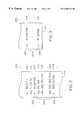
- FIG. 2shows an instruction stream 201 as it enters the instruction queue 110 of FIG. 1 . Instructions are placed in the queue 110 in the order in which they are encountered in the stream 201 .
- the instruction labeled 203“st R 7 , 0 (R 30 )” is a store instruction. When it is executed at stage 5 of FIG. 1, the data in register R 7 is stored in a target memory location whose address is the sum of 0 and the contents held in register R 30 . This target address must be computed during the execution stage 5 of the instruction pipeline 100 (FIG. 1 ).
- the instruction labeled 205“ld R 29 , 0 (R 30 )” is a load instruction.
- the memory locationis referenced whose address is again the sum of 0 and the contents held in register R 30 , and the data held in this referenced memory location is loaded into register R 29 .
- Other instructions 207may be fetched between store instruction 203 and load instruction 205 .
- the load instruction 205is dependent on the store instruction 203 because the load instruction 205 needs to read the data stored in memory by the store instruction 203 .
- instructions from stream 201enter the instruction queue 110 , they are assigned instruction numbers (INUM) 209 , here shown in decimal form. Specifically, a value of 1012 has been assigned as the INUM to the store instruction 203 , and a value of 1024 has been assigned as the INUM to the load instruction 205 .
- a re-ordered issue stream 301is shown in FIG. 3 .
- the load 205 and store 203 instructionshave issued out-of-order. This could be, for example, because register R 7 is not yet available to the store instruction 203 .
- register R 30contains the same value for both instructions 203 , 205 , the load instruction 205 will potentially be reading in the wrong data because it needs the data to be stored by the store instruction 203 .
- the present inventionprovides a bypass mechanism that compares the address of each load instruction with a set of recent stores that have not yet updated memory. A match of the recent stores provides the desired load data instead of having to retrieve the data from memory.
- the data cache subsystem 420operates in conjunction with an execution unit 418 that performs load/store processing associated with pipeline stage 5 (FIG. 1 ).
- the data cache subsystem 420includes a decode unit 422 , a translation look-aside buffer (TLB) 424 , a store queue 426 , a store data buffer 428 and a data cache (dcache) unit 430 .
- the dcache unit 430is a 64 KB, 2-way set-associative, virtually-indexed and physically-tagged data cache.
- the dcache unit 430includes tag store 432 , data store 434 , hit compare logic 436 and multiplexer 438 .
- the data cache subsystemincludes a decode unit which examines the Opcode of the issuing instruction. Information such as whether the operation is a load or store is extracted. Also extracted is information such as whether the data type is Integer data or Floating-Point data, and what the data size is, Quadword, Longword, Word, or Byte.
- the dcache unit 430is formed by several lines 24 A, 24 B in the tag store 432 and data store 434 .
- Each line 24 A, 24 Bincludes a tag 26 and a block 28 of words 30 .
- the tag 26is associated with the four word block 28 .
- An indexis used to select a particular line 24 A, 24 B and word 30 of the dcache unit 430 .
- FIG. 6shows an exemplary 64-bit virtual address format 32 and an exemplary 44-bit physical address 34 .
- Bits 13 through 63(denoted bits 63 : 13 ) for the virtual address 32 indicate a virtual page number.
- the remaining bitsi.e., bits 12 : 0 ) for both the virtual address 32 and the physical address 34 indicate the byte within page.
- Bits 0 through 14i.e., bits 14 : 0
- Bits 13 through 43i.e., bits 43 : 13
- the TLB 424contains entries that provide the mapping function between the virtual addresses used by the execution unit 418 and the physical addresses used by the dcache 430 .
- cache accessproceeds as follows.
- a virtual addressis input from the execution unit 418 to the TLB 424 where it is translated into a physical address.
- the virtual addressis also parsed to form a virtual index into the dcache unit 430 to address the appropriate cache location.
- the tag for such locationis then compared with a tag reference formed from a parse of the translated physical address using hit compare logic 436 . If the tag and the tag reference match, then there is a cache hit and the corresponding data word in the data store 434 is passed to the execution unit 418 on load/store data (LSD) bus 464 . If there is not a tag match, then there is a cache miss and the data is fetched from external memory (not shown).
- LSDload/store data
- FIG. 7shows the structure of the store queue 426 and store data buffer 428 .
- Several lines 40 A, 40 B of store instructionsare held in the store queue 426 and store data buffer 428 , respectively.
- Each line portion 40 A of the store queue 426includes a physical address 42 , an INUM field 44 , a NO HIT bit 46 and a size field 48 .
- the NO HIT bitserves as a match status indicator and the size field serves as a data size indicator.
- Each corresponding line portion 40 Bincludes a block 50 of words 52 .
- a flow diagramis there shown which generally illustrates the operation of the store queue bypass mechanism of the present invention.
- a virtual addressis provided by the execution unit 418 and is input at block 504 to the TLB 424 for translation into a physical address.
- the tag store 432 and the store queue 426are queried using bits 14 : 0 of the virtual address for the virtual index and bits 43 : 13 of the translated physical address for the tag comparison. If there is a match in the store queue 426 at block 510 , then corresponding data is read from the store data buffer 428 at block 512 .
- the match in the store queue 426is indicated by asserting STQ control line 456 .
- Assertion of STQ control line 456 at multiplexer 438selects bypass input 460 from store data buffer 428 , and the data on bypass line 460 is passed to the execution unit 418 on LSD bus 464 .
- FIG. 9shows an exemplary issue stream 602 in which the instruction labeled 604 , “stl R 2 , 0 (R 7 )” is a store instruction wherein the “stl” refers to storing a long word (4 data bytes).
- the instruction labeled 606 , “ldq R 29 , 0 (R 7 )”is a load instruction wherein the “ldq” refers to loading a quad word (8 data bytes).
- the load instructionneeds to access bytes that are in memory in addition to bytes that are available through the bypass mechanism.
- the present inventionprovides a methodology and apparatus for detecting this mismatch in data size.
- the available address bitsi.e., virtual address bits 14 : 0
- the issue INUM 450 (FIG. 4) of the issuing loadis compared against the INUM field 44 (FIG. 7) of each store queue entry. If the addresses match and the INUM compare indicates that the load is younger in program order than the particular matching store queue entry, then the bypass mechanism is activated.
- the store queue 426Two cycles later the store queue 426 (FIG. 4) is presented with the full physical address of the issuing load. This time the full physical address is compared against each entry in the store queue 426 .
- the size field 48 (FIG. 7) of the store queue entryis compared against the size information of the issuing load. If the address matches and the INUM compare indicates that the load is younger than the matching store, but the size information indicates that the data size of the matching store is smaller than that of the issuing load, then the store queue 426 provides a TRAP signal 454 .
- the TRAP signal 454indicates that the data provided by the bypass mechanism was insufficient to satisfy the requirements of the load instruction and therefore, the in-flight instructions should be killed.
- the present inventionprovides a methodology and apparatus for determining which of the multiple stores should be used in bypassing the dcache unit 430 .
- the available address bitsare compared against each valid entry of the store queue 426 . If the address matches and the INUM comparison indicates that the issuing store is younger than the matching store, then the NO HIT bit 46 (FIG. 7) of that matching store queue entry is set. However, if the INUM comparison indicates that the issuing store is older than the matching store, then the NO HIT bit 46 of the issuing store is set. This mechanism of checking the INUM values and setting the appropriate NO HIT bit is an attempt to provide the data of the most recent store to a subsequently issuing load and thereby avoid getting older data to the load.
- the available address bitsare compared against valid entries in the store queue 426 . If the address matches, and the INUM comparison indicates that the load is younger in program order than the matching store, then the bypass mechanism is activated, unless the NO HIT bit 46 of the matching store queue entry is set.
- the store queue 426Two cycles later the store queue 426 is presented with the full physical address of the issuing load. This time the full physical address is compared against each entry in the store queue 426 . If the address matches and the INUM comparison indicates that the load is younger than the matching store, but the data bypass was not activated, then the store queue 426 signals a TRAP signal 454 .
- the TRAP signal 454indicates that the data bypass mechanism did not provide data when it should have and therefore, the in-flight instructions should be killed.
- FIG. 10illustrates a case in which multiple stores are made to the same address location.
- a program stream 610is shown with program instructions 614 , 616 and 618 that reference the same address.
- Program instruction 620references a different address.
- Each program instructionhas an associated INUM value, e.g., store instruction 614 has an INUM value equal to 13 while store instruction 618 has an INUM value of 15. Thus, store instruction 614 is older in program order than store instruction 618 .
- Issue stream 612shows these instructions in issue order, that is, store instruction 614 is followed by store instruction 618 , load instruction 616 and then store instruction 620 .
- Store instructions 614 and 618reference the same address. Based on the mechanism described above for setting the NO HIT bit 46 (FIG. 7) for multiple stores to the same address, the NO HIT bit for store instruction 614 has been set, indicating that store instruction 618 should be the most recent store to provide data to a subsequent load.
- the available address bitsare compared against each valid entry in the store queue 426 . If the addresses match, and the INUM comparison indicates that the load is younger than the matching store, then the bypass is activated.
- the store queue 426signals a TRAP signal 454 .
- the TRAP signalin this case indicates that the data bypass mechanism was activated when in fact it was not appropriate.
Landscapes
- Engineering & Computer Science (AREA)
- Software Systems (AREA)
- Theoretical Computer Science (AREA)
- Physics & Mathematics (AREA)
- General Engineering & Computer Science (AREA)
- General Physics & Mathematics (AREA)
- Memory System Of A Hierarchy Structure (AREA)
Abstract
Description
Claims (12)
Priority Applications (1)
| Application Number | Priority Date | Filing Date | Title |
|---|---|---|---|
| US09/115,186US6360314B1 (en) | 1998-07-14 | 1998-07-14 | Data cache having store queue bypass for out-of-order instruction execution and method for same |
Applications Claiming Priority (1)
| Application Number | Priority Date | Filing Date | Title |
|---|---|---|---|
| US09/115,186US6360314B1 (en) | 1998-07-14 | 1998-07-14 | Data cache having store queue bypass for out-of-order instruction execution and method for same |
Publications (1)
| Publication Number | Publication Date |
|---|---|
| US6360314B1true US6360314B1 (en) | 2002-03-19 |
Family
ID=22359786
Family Applications (1)
| Application Number | Title | Priority Date | Filing Date |
|---|---|---|---|
| US09/115,186Expired - Fee RelatedUS6360314B1 (en) | 1998-07-14 | 1998-07-14 | Data cache having store queue bypass for out-of-order instruction execution and method for same |
Country Status (1)
| Country | Link |
|---|---|
| US (1) | US6360314B1 (en) |
Cited By (24)
| Publication number | Priority date | Publication date | Assignee | Title |
|---|---|---|---|---|
| US20010056517A1 (en)* | 2000-06-26 | 2001-12-27 | Makoto Hataida | Data processing device |
| US20030172235A1 (en)* | 2002-02-27 | 2003-09-11 | Letey George Thomas | Read data storage controller with bypass read data return path |
| US6658554B1 (en)* | 1999-03-09 | 2003-12-02 | Wisconsin Alumni Res Found | Electronic processor providing direct data transfer between linked data consuming instructions |
| US6681320B1 (en) | 1999-12-29 | 2004-01-20 | Intel Corporation | Causality-based memory ordering in a multiprocessing environment |
| US6725358B1 (en)* | 2000-06-22 | 2004-04-20 | International Business Machines Corporation | Processor and method having a load reorder queue that supports reservations |
| US20050010744A1 (en)* | 2003-07-08 | 2005-01-13 | Advanced Micro Devices, Inc. | Store-to-load forwarding buffer using indexed lookup |
| US6862676B1 (en) | 2001-01-16 | 2005-03-01 | Sun Microsystems, Inc. | Superscalar processor having content addressable memory structures for determining dependencies |
| US6868491B1 (en)* | 2000-06-22 | 2005-03-15 | International Business Machines Corporation | Processor and method of executing load instructions out-of-order having reduced hazard penalty |
| US20050138339A1 (en)* | 2003-12-23 | 2005-06-23 | Intel Corporation | Method for and a trailing store buffer for use in memory renaming |
| US20060174083A1 (en)* | 2005-02-03 | 2006-08-03 | Barrick Brian D | Method of load/store dependencies detection with dynamically changing address length |
| US7269825B1 (en)* | 2002-12-27 | 2007-09-11 | Unisys Corporation | Method and system for relative address translation |
| US20070294693A1 (en)* | 2006-06-16 | 2007-12-20 | Microsoft Corporation | Scheduling thread execution among a plurality of processors based on evaluation of memory access data |
| US20090013135A1 (en)* | 2007-07-05 | 2009-01-08 | Board Of Regents, The University Of Texas System | Unordered load/store queue |
| US20090319727A1 (en)* | 2008-06-23 | 2009-12-24 | Dhodapkar Ashutosh S | Efficient Load Queue Snooping |
| US7779236B1 (en)* | 1998-12-31 | 2010-08-17 | Stmicroelectronics, Inc. | Symbolic store-load bypass |
| US20100332806A1 (en)* | 2009-06-30 | 2010-12-30 | Golla Robert T | Dependency matrix for the determination of load dependencies |
| US20110138162A1 (en)* | 2009-12-08 | 2011-06-09 | Scott Chiu | Reconfigurable load-reduced memory buffer |
| US8949583B1 (en) | 2004-09-14 | 2015-02-03 | Azul Systems, Inc. | Concurrent atomic execution |
| US9304936B2 (en) | 2013-12-09 | 2016-04-05 | International Business Machines Corporation | Bypassing a store-conditional request around a store queue |
| US20160179160A1 (en)* | 2014-12-17 | 2016-06-23 | International Business Machines Corporation | Design structure for reducing power consumption for memory device |
| US20170046271A1 (en)* | 2015-08-13 | 2017-02-16 | Freescale Semiconductor, Inc. | Tagged Cache For Data Coherency In Multi-Domain Debug Operations |
| CN107220032A (en)* | 2012-06-15 | 2017-09-29 | 英特尔公司 | Without the out of order load store queue of disambiguation |
| US9928071B1 (en)* | 2008-05-02 | 2018-03-27 | Azul Systems, Inc. | Enhanced managed runtime environments that support deterministic record and replay |
| WO2021108086A1 (en) | 2019-11-27 | 2021-06-03 | Advanced Micro Devices, Inc. | Techniques for performing store-to-load forwarding |
Citations (10)
| Publication number | Priority date | Publication date | Assignee | Title |
|---|---|---|---|---|
| US5307477A (en) | 1989-12-01 | 1994-04-26 | Mips Computer Systems, Inc. | Two-level cache memory system |
| US5448699A (en)* | 1990-12-21 | 1995-09-05 | Compaq Computer Corp. | Apparatus with leading edge delay circuit for selectively sending a delayed substitute version of a signal transmitted between an expansion card and a system bus |
| US5479630A (en) | 1991-04-03 | 1995-12-26 | Silicon Graphics Inc. | Hybrid cache having physical-cache and virtual-cache characteristics and method for accessing same |
| US5557763A (en)* | 1992-09-29 | 1996-09-17 | Seiko Epson Corporation | System for handling load and/or store operations in a superscalar microprocessor |
| US5613081A (en) | 1994-03-04 | 1997-03-18 | Motorola, Inc. | Method of operating a data processor with rapid address comparison for data forwarding |
| US5619662A (en) | 1992-11-12 | 1997-04-08 | Digital Equipment Corporation | Memory reference tagging |
| US5717883A (en)* | 1995-06-28 | 1998-02-10 | Digital Equipment Corporation | Method and apparatus for parallel execution of computer programs using information providing for reconstruction of a logical sequential program |
| US5737636A (en) | 1996-01-18 | 1998-04-07 | International Business Machines Corporation | Method and system for detecting bypass errors in a load/store unit of a superscalar processor |
| US5867644A (en)* | 1996-09-10 | 1999-02-02 | Hewlett Packard Company | System and method for on-chip debug support and performance monitoring in a microprocessor |
| US5897666A (en)* | 1996-12-09 | 1999-04-27 | International Business Machines Corporation | Generation of unique address alias for memory disambiguation buffer to avoid false collisions |
- 1998
- 1998-07-14USUS09/115,186patent/US6360314B1/ennot_activeExpired - Fee Related
Patent Citations (10)
| Publication number | Priority date | Publication date | Assignee | Title |
|---|---|---|---|---|
| US5307477A (en) | 1989-12-01 | 1994-04-26 | Mips Computer Systems, Inc. | Two-level cache memory system |
| US5448699A (en)* | 1990-12-21 | 1995-09-05 | Compaq Computer Corp. | Apparatus with leading edge delay circuit for selectively sending a delayed substitute version of a signal transmitted between an expansion card and a system bus |
| US5479630A (en) | 1991-04-03 | 1995-12-26 | Silicon Graphics Inc. | Hybrid cache having physical-cache and virtual-cache characteristics and method for accessing same |
| US5557763A (en)* | 1992-09-29 | 1996-09-17 | Seiko Epson Corporation | System for handling load and/or store operations in a superscalar microprocessor |
| US5619662A (en) | 1992-11-12 | 1997-04-08 | Digital Equipment Corporation | Memory reference tagging |
| US5613081A (en) | 1994-03-04 | 1997-03-18 | Motorola, Inc. | Method of operating a data processor with rapid address comparison for data forwarding |
| US5717883A (en)* | 1995-06-28 | 1998-02-10 | Digital Equipment Corporation | Method and apparatus for parallel execution of computer programs using information providing for reconstruction of a logical sequential program |
| US5737636A (en) | 1996-01-18 | 1998-04-07 | International Business Machines Corporation | Method and system for detecting bypass errors in a load/store unit of a superscalar processor |
| US5867644A (en)* | 1996-09-10 | 1999-02-02 | Hewlett Packard Company | System and method for on-chip debug support and performance monitoring in a microprocessor |
| US5897666A (en)* | 1996-12-09 | 1999-04-27 | International Business Machines Corporation | Generation of unique address alias for memory disambiguation buffer to avoid false collisions |
Non-Patent Citations (3)
| Title |
|---|
| Gieseke, B. A., et al., "A 600MHz Superscalar RISC Microprocessor with Out-Of-Order Execution," 1997 IEEE Internaional Solid-State Circuits Conference, Dig. Tech. Papers, pp. 176-177 and 451 (Feb., 1997). |
| Gwennap, L., "Digital 21264 Sets New Standard," Microprocessor Report, pp. 11-16 (Oct. 28, 1996). |
| Leibholz, D. and Razdan, R., "The Alpha 21264: A 500 MHZ Out-Of-Order Execution Microprocessor," Proceedings of IEEE COMPCON '97, (Feb., 1997). |
Cited By (47)
| Publication number | Priority date | Publication date | Assignee | Title |
|---|---|---|---|---|
| US7779236B1 (en)* | 1998-12-31 | 2010-08-17 | Stmicroelectronics, Inc. | Symbolic store-load bypass |
| US6658554B1 (en)* | 1999-03-09 | 2003-12-02 | Wisconsin Alumni Res Found | Electronic processor providing direct data transfer between linked data consuming instructions |
| US6681320B1 (en) | 1999-12-29 | 2004-01-20 | Intel Corporation | Causality-based memory ordering in a multiprocessing environment |
| US6725358B1 (en)* | 2000-06-22 | 2004-04-20 | International Business Machines Corporation | Processor and method having a load reorder queue that supports reservations |
| US6868491B1 (en)* | 2000-06-22 | 2005-03-15 | International Business Machines Corporation | Processor and method of executing load instructions out-of-order having reduced hazard penalty |
| US20010056517A1 (en)* | 2000-06-26 | 2001-12-27 | Makoto Hataida | Data processing device |
| US6442665B2 (en)* | 2000-06-26 | 2002-08-27 | Fujitsu Limited | Data processing device |
| US6862676B1 (en) | 2001-01-16 | 2005-03-01 | Sun Microsystems, Inc. | Superscalar processor having content addressable memory structures for determining dependencies |
| US20030172235A1 (en)* | 2002-02-27 | 2003-09-11 | Letey George Thomas | Read data storage controller with bypass read data return path |
| US7269825B1 (en)* | 2002-12-27 | 2007-09-11 | Unisys Corporation | Method and system for relative address translation |
| GB2420202B (en)* | 2003-07-08 | 2006-12-06 | Advanced Micro Devices Inc | Store-to-load forwarding buffer using indexed lookup |
| US20050010744A1 (en)* | 2003-07-08 | 2005-01-13 | Advanced Micro Devices, Inc. | Store-to-load forwarding buffer using indexed lookup |
| US7321964B2 (en)* | 2003-07-08 | 2008-01-22 | Advanced Micro Devices, Inc. | Store-to-load forwarding buffer using indexed lookup |
| DE112004001248B4 (en) | 2003-07-08 | 2008-08-21 | Advanced Micro Devices, Inc., Sunnyvale | A microprocessor and method for performing indexed store-to-load forwarding |
| US7640419B2 (en)* | 2003-12-23 | 2009-12-29 | Intel Corporation | Method for and a trailing store buffer for use in memory renaming |
| US20050138339A1 (en)* | 2003-12-23 | 2005-06-23 | Intel Corporation | Method for and a trailing store buffer for use in memory renaming |
| US8949583B1 (en) | 2004-09-14 | 2015-02-03 | Azul Systems, Inc. | Concurrent atomic execution |
| US7464242B2 (en)* | 2005-02-03 | 2008-12-09 | International Business Machines Corporation | Method of load/store dependencies detection with dynamically changing address length |
| US20060174083A1 (en)* | 2005-02-03 | 2006-08-03 | Barrick Brian D | Method of load/store dependencies detection with dynamically changing address length |
| US20070294693A1 (en)* | 2006-06-16 | 2007-12-20 | Microsoft Corporation | Scheduling thread execution among a plurality of processors based on evaluation of memory access data |
| US8447911B2 (en)* | 2007-07-05 | 2013-05-21 | Board Of Regents, University Of Texas System | Unordered load/store queue |
| US20090013135A1 (en)* | 2007-07-05 | 2009-01-08 | Board Of Regents, The University Of Texas System | Unordered load/store queue |
| WO2009006595A1 (en)* | 2007-07-05 | 2009-01-08 | Board Of Regents, University Of Texas System | Unordered load/store queue |
| US9928071B1 (en)* | 2008-05-02 | 2018-03-27 | Azul Systems, Inc. | Enhanced managed runtime environments that support deterministic record and replay |
| US10671400B2 (en) | 2008-05-02 | 2020-06-02 | Azul Systems, Inc. | Enhanced managed runtime environments that support deterministic record and replay |
| US9928072B1 (en) | 2008-05-02 | 2018-03-27 | Azul Systems, Inc. | Detecting and recording atomic execution |
| WO2010008460A1 (en)* | 2008-06-23 | 2010-01-21 | Advanced Micro Devices, Inc. | Efficient load queue snooping |
| US20090319727A1 (en)* | 2008-06-23 | 2009-12-24 | Dhodapkar Ashutosh S | Efficient Load Queue Snooping |
| US8214602B2 (en) | 2008-06-23 | 2012-07-03 | Advanced Micro Devices, Inc. | Efficient load queue snooping |
| CN102132248B (en)* | 2008-06-23 | 2014-11-12 | 超威半导体公司 | Efficient loading queue snooping |
| US20100332806A1 (en)* | 2009-06-30 | 2010-12-30 | Golla Robert T | Dependency matrix for the determination of load dependencies |
| US9262171B2 (en) | 2009-06-30 | 2016-02-16 | Oracle America, Inc. | Dependency matrix for the determination of load dependencies |
| US20110138162A1 (en)* | 2009-12-08 | 2011-06-09 | Scott Chiu | Reconfigurable load-reduced memory buffer |
| US8688901B2 (en)* | 2009-12-08 | 2014-04-01 | Intel Corporation | Reconfigurable load-reduced memory buffer |
| US9305613B2 (en) | 2009-12-08 | 2016-04-05 | Intel Corporation | Reconfigurable load-reduced memory buffer |
| CN107220032A (en)* | 2012-06-15 | 2017-09-29 | 英特尔公司 | Without the out of order load store queue of disambiguation |
| CN107220032B (en)* | 2012-06-15 | 2020-12-15 | 英特尔公司 | Disambiguation-free out-of-order load store queue |
| US9304936B2 (en) | 2013-12-09 | 2016-04-05 | International Business Machines Corporation | Bypassing a store-conditional request around a store queue |
| US9390024B2 (en) | 2013-12-09 | 2016-07-12 | International Business Machines Corporation | Bypassing a store-conditional request around a store queue |
| US20160179160A1 (en)* | 2014-12-17 | 2016-06-23 | International Business Machines Corporation | Design structure for reducing power consumption for memory device |
| US9946588B2 (en)* | 2014-12-17 | 2018-04-17 | International Business Machines Corporation | Structure for reducing power consumption for memory device |
| US9946589B2 (en) | 2014-12-17 | 2018-04-17 | International Business Machines Corporation | Structure for reducing power consumption for memory device |
| US9652401B2 (en)* | 2015-08-13 | 2017-05-16 | Nxp Usa, Inc. | Tagged cache for data coherency in multi-domain debug operations |
| US20170046271A1 (en)* | 2015-08-13 | 2017-02-16 | Freescale Semiconductor, Inc. | Tagged Cache For Data Coherency In Multi-Domain Debug Operations |
| WO2021108086A1 (en) | 2019-11-27 | 2021-06-03 | Advanced Micro Devices, Inc. | Techniques for performing store-to-load forwarding |
| JP2023503577A (en)* | 2019-11-27 | 2023-01-31 | アドバンスト・マイクロ・ディバイシズ・インコーポレイテッド | Techniques for performing store-to-load transfers |
| EP4066120A4 (en)* | 2019-11-27 | 2023-12-20 | Advanced Micro Devices, Inc. | METHOD FOR PERFORMING STORE-TO-LOAD FORWARDING |
Similar Documents
| Publication | Publication Date | Title |
|---|---|---|
| US6360314B1 (en) | Data cache having store queue bypass for out-of-order instruction execution and method for same | |
| US6463523B1 (en) | Method and apparatus for delaying the execution of dependent loads | |
| US5615350A (en) | Apparatus to dynamically control the out-of-order execution of load-store instructions in a processor capable of dispatching, issuing and executing multiple instructions in a single processor cycle | |
| US7568087B2 (en) | Partial load/store forward prediction | |
| US5751983A (en) | Out-of-order processor with a memory subsystem which handles speculatively dispatched load operations | |
| JP3874022B2 (en) | Computer system | |
| EP2674856B1 (en) | Zero cycle load instruction | |
| EP0380859B1 (en) | Method of preprocessing multiple instructions | |
| US7213126B1 (en) | Method and processor including logic for storing traces within a trace cache | |
| US6622237B1 (en) | Store to load forward predictor training using delta tag | |
| US6651161B1 (en) | Store load forward predictor untraining | |
| EP0381470A2 (en) | Processing of memory access exceptions along with prefetched instructions within the instruction pipeline of a virtual memory system-based digital computer | |
| US7174428B2 (en) | Method and system for transforming memory location references in instructions | |
| JPH07325716A (en) | Pipeline processor and its operating method | |
| US8171240B1 (en) | Misalignment predictor | |
| US20070050592A1 (en) | Method and apparatus for accessing misaligned data streams | |
| US20070130448A1 (en) | Stack tracker | |
| US7321964B2 (en) | Store-to-load forwarding buffer using indexed lookup | |
| EP0912929A1 (en) | A data address prediction structure and a method for operating the same |
Legal Events
| Date | Code | Title | Description |
|---|---|---|---|
| AS | Assignment | Owner name:DIGITAL EQUIPMENT CORPORATION, MASSACHUSETTS Free format text:ASSIGNMENT OF ASSIGNORS INTEREST;ASSIGNORS:WEBB, DAVID ARTHUR JAMES, JR.;KELLER, JAMES B.;MEYER, DERRICK R.;REEL/FRAME:009373/0219;SIGNING DATES FROM 19980706 TO 19980713 | |
| AS | Assignment | Owner name:COMPAQ COMPUTER CORPORATION, TEXAS Free format text:MERGER;ASSIGNOR:DIGITAL EQUIPMENT CORPORATION;REEL/FRAME:011776/0688 Effective date:19991209 | |
| AS | Assignment | Owner name:COMPAQ INFORMATION TECHNOLOGIES GROUP, L.P., TEXAS Free format text:ASSIGNMENT OF ASSIGNORS INTEREST;ASSIGNOR:COMPAQ COMPUTER CORPORATION;REEL/FRAME:012465/0596 Effective date:20010620 | |
| AS | Assignment | Owner name:HEWLETT-PACKARD DEVELOPMENT COMPANY, L.P., TEXAS Free format text:CHANGE OF NAME;ASSIGNOR:COMPAQ INFORMATION TECHNOLOGIES GROUP L.P.;REEL/FRAME:016600/0125 Effective date:20021001 | |
| FPAY | Fee payment | Year of fee payment:4 | |
| FEPP | Fee payment procedure | Free format text:PAYER NUMBER DE-ASSIGNED (ORIGINAL EVENT CODE: RMPN); ENTITY STATUS OF PATENT OWNER: LARGE ENTITY Free format text:PAYOR NUMBER ASSIGNED (ORIGINAL EVENT CODE: ASPN); ENTITY STATUS OF PATENT OWNER: LARGE ENTITY | |
| FPAY | Fee payment | Year of fee payment:8 | |
| REMI | Maintenance fee reminder mailed | ||
| LAPS | Lapse for failure to pay maintenance fees | ||
| STCH | Information on status: patent discontinuation | Free format text:PATENT EXPIRED DUE TO NONPAYMENT OF MAINTENANCE FEES UNDER 37 CFR 1.362 | |
| FP | Lapsed due to failure to pay maintenance fee | Effective date:20140319 |