US6359810B1 - Page mode erase in a flash memory array - Google Patents
Page mode erase in a flash memory arrayDownload PDFInfo
- Publication number
- US6359810B1 US6359810B1US09/542,434US54243400AUS6359810B1US 6359810 B1US6359810 B1US 6359810B1US 54243400 AUS54243400 AUS 54243400AUS 6359810 B1US6359810 B1US 6359810B1
- Authority
- US
- United States
- Prior art keywords
- volts
- voltage
- memory cell
- positive
- flash memory
- Prior art date
- Legal status (The legal status is an assumption and is not a legal conclusion. Google has not performed a legal analysis and makes no representation as to the accuracy of the status listed.)
- Expired - Lifetime
Links
- 230000005641tunnelingEffects0.000claimsabstractdescription10
- 238000000034methodMethods0.000claims11
- 238000002955isolationMethods0.000description9
- PWPJGUXAGUPAHP-UHFFFAOYSA-NlufenuronChemical compoundC1=C(Cl)C(OC(F)(F)C(C(F)(F)F)F)=CC(Cl)=C1NC(=O)NC(=O)C1=C(F)C=CC=C1FPWPJGUXAGUPAHP-UHFFFAOYSA-N0.000description7
- 230000000295complement effectEffects0.000description3
- 238000010586diagramMethods0.000description3
- 238000005513bias potentialMethods0.000description2
- 238000003491arrayMethods0.000description1
- 239000002784hot electronSubstances0.000description1
- 238000002347injectionMethods0.000description1
- 239000007924injectionSubstances0.000description1
- 239000011159matrix materialSubstances0.000description1
- 238000012986modificationMethods0.000description1
- 230000004048modificationEffects0.000description1
- 239000007787solidSubstances0.000description1
Images


Classifications
- G—PHYSICS
- G11—INFORMATION STORAGE
- G11C—STATIC STORES
- G11C5/00—Details of stores covered by group G11C11/00
- G11C5/14—Power supply arrangements, e.g. power down, chip selection or deselection, layout of wirings or power grids, or multiple supply levels
- G11C5/147—Voltage reference generators, voltage or current regulators; Internally lowered supply levels; Compensation for voltage drops
- G—PHYSICS
- G11—INFORMATION STORAGE
- G11C—STATIC STORES
- G11C16/00—Erasable programmable read-only memories
- G11C16/02—Erasable programmable read-only memories electrically programmable
- G11C16/06—Auxiliary circuits, e.g. for writing into memory
- G11C16/10—Programming or data input circuits
- G11C16/14—Circuits for erasing electrically, e.g. erase voltage switching circuits
- G11C16/16—Circuits for erasing electrically, e.g. erase voltage switching circuits for erasing blocks, e.g. arrays, words, groups
Definitions
- the present inventionrelates to the erase mode in a flash memory array. More particularly, the present invention relates to a page erase mode and multiple page erase mode in a flash memory array.
- the flash memory arrayis typically arranged as a matrix of wordlines and bitlines to form intersections with flash memory elements disposed at the intersections in a manner well known to those of ordinary skill in the art.
- the operations that may be performed on the memory cells in the flash memory arrayare READ, PROGRAM and ERASE.
- the PROGRAM operationis often performed by driving selected bitlines connected to the drain region in the flash memory cells to a first voltage and driving the gates of the flash memory cells connected to selected wordlines to a higher voltage to perform hot electron injection in a manner well known to those of ordinary skill in the art.
- the ERASE operationis performed by driving the gate of the flash memory cell to a voltage that is substantially less than a voltage placed on the bitline. In doing so, electrons are tunneled off of the floating gate of the flash memory cells in a manner well known to those of ordinary skill in the art.
- BULK ERASEa voltage that is substantially less than a voltage placed on the bitline.
- SECTOR ERASEa sector in the flash memory array may be erased at one time.
- An example of a BULK ERASE of a flash memory arrayis found in the paper “A 90 ns 100K Erase-Program Cycle Megabit Flash Memory”, 1989, IEEE International Solid State Circuits Conference, pages 140 and 141, February 1989.
- Constraining the ERASE operation to either a SECTOR or BULK ERASEis done in consideration of the fact that when individual row lines are selected to be erased, there is the possibility the value stored on the floating gate of flash memory cells for unselected rows will be affected due to the occurrence of unintended tunneling. Accordingly, it is an object of the present invention to provide an erase mode wherein only a single row in a sector or multiple rows in a sector may be erased while reducing the disturb phenomenon for flash memory cells in the sector that are not selected.
- a MULTIPLE PAGE ERASE modeis provided.
- the rows in a sectorare partitioned into groups, and more than one row in the group is selected to be erased or corresponding rows in different groups are selected to be erased.
- a preferred tunneling voltage of approximately ⁇ 10 Volts to the gates of the flash memory cells in the rows selected for erasure, and the bitlines connected to the drains of the flash memory cellsare driven to a preferred voltage of approximately 6.5 Volts.
- a preferred bias voltageof approximately 1 to 2 Volts is applied to the gates of the flash memory cells in rows that have not been selected for erasure.
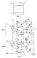
- FIG. 1illustrates a block diagram of flash memory array according to the present invention.
- FIG. 3illustrates a table of signals applied to elements in the sector illustrated in FIG. 2 for the READ, PROGRAM AND PAGE ERASE modes of a flash memory array according to the present invention.
- FIG. 4illustrates a schematic diagram of variable reference generator circuit suitable for use according to the present invention.
- a flash memory array 10according to the present invention is illustrated.
- the flash memory array 10has M rows, wherein each row has N bytes.
- Each of the M rows in the flash memory array 10is typically referred to as a page of memory.
- the M rowsare grouped into sectors or blocks in a manner well known to those of ordinary skill in the art. It will be appreciated that the number of rows included in a sector of the flash memory array 10 is typically a matter of design choice, and further that the entire flash memory array 10 may be considered as one sector.
- 2,048 rows (or pages) of 264 byteseach are grouped into 4 sectors containing 512 rows apiece.
- an erase of the entire flash memory array at onceknown as a BULK ERASE
- SECTOR ERASEan erase of an entire sector
- an erasemay be performed on a single row in a sector, known as PAGE ERASE, or on multiple pages in a sector known as MULTIPLE PAGE ERASE.
- FIG. 2a portion 14 of a sector 12 according to the present invention is illustrated.
- the rows 20are separated into K groups, wherein each of the K groups has J rows.
- the 512 rows in the sectorare divided into 64 groups, wherein each of the 64 groups includes 8 rows.
- a first group of rows 20 - 1 through 20 -Jis shown as Group 1
- a last group of rows 20 - 1 through 20 -Jis shown as Group K.
- Each of the rows 20 - 1 through 20 -J in the flash memory array 10is a wordline as is well understood by those of ordinary skill in the art.
- Each of the word lines of rows 20 - 1 through 20 -Jform intersections with bit lines.
- the number of bitlines in the flash memory arrayis equal to the number of words in the row 20 multiplied by the number of bits in each word.
- a single bit line 22is depicted for illustrative purposes.
- flash memory cells 24Disposed at the intersections between the word lines 20 and the bit lines 22 are flash memory cells 24 .
- a specific embodiment of a flash memory cellwill not be described herein to avoid over complicating the disclosure, and thereby obscuring the present invention.
- a flash memory cell suitable for use according to the present inventionis described in U.S. Pat. No. 4,783,766, filed May 30, 1986, assigned to the same assignee as the present invention, and incorporated herein by reference.
- each wordline 20Connected to one end of each wordline 20 is a pair of N-channel MOS transistors 26 - 1 and 26 - 2 .
- the drain of the first N-channel MOS transistor 26 - 1is connected to a row selection potential, Xd
- the source of the second N-channel MOS transistor 26 - 2is connected to a gate bias potential Vwg
- the source and drain of first N-channel MOS transistor 26 - 1 and second N-channel MOS transistor 26 - 2are connected to the word lines 20 .
- each N-channel MOS transistor 26 - 1is connected to a group selection signal, Xs
- the gate of each N-channel MOS transistor 26 - 2is connected to the compliment, ⁇ overscore (Xs) ⁇ , of the group selection signal, Xs, provided by inverter 28 .
- the inverter 28provides a voltage potential on ⁇ overscore (Xs) ⁇ that is either higher or lower than the voltage on Xs by a desired amount.
- the group select signal, Xs, and its compliment, ⁇ overscore (Xs) ⁇ ,are provided by a decoder, the implementation of which is well within the purview of those of ordinary skill in the art, and which will not be disclosed herein to avoid over complicating the disclosure and thereby obscuring the present invention.
- the drain of the flash memory elementis connected to the bit line 22
- the source of the flash memory element 24is connected to an array source voltage by an array source line 30
- the gate of the flash memory element 24is connected to the word line 20 .
- a P-channel MOS isolation pass transistor 32is connected in series between each pair of N-channel MOS transistors 26 - 1 and 26 - 2 and the first flash memory element 24 disposed at the intersection of the wordline 20 and a bit line 22 .
- a word line pump 34Connected to the portion of each word line 20 disposed between P-channel MOS isolation pass transistor 32 and the gate of the first flash memory element 24 disposed at the intersection of the wordline 20 and a bit line 22 is a word line pump 34 connected to a source of negative voltage of about ⁇ 15 volts to about ⁇ 4 volts, and preferably ⁇ 10 volts, by word line pump line 36 .
- FIG. 3a table indicating the signals applied to various elements in the circuit illustrated in FIG. 2 to implement the READ, PROGRAMMING and ERASE modes of the flash memory array according to the present invention are depicted. According to the present invention, only the application of the signals made during the ERASE operation will be described herein.
- a Vcc voltageis applied on the group select signal line, Xs, to the gates of the N-channel MOS transistors 26 - 1 in the group containing the row 20 - 1 through 20 -j being selected for PAGE ERASE, and a ground voltage (0 volts) is applied on the complement of the group select signal line, ⁇ overscore (Xs) ⁇ , to the gates of the N-channel MOS transistors 26 - 2 in the group containing the row 20 - 1 through 20 -j being selected for PAGE ERASE.
- a ground voltage (0 volts)is applied on the group select signal line, Xs, to the gates of the N-channel MOS transistors 26 - 1
- Vcc voltageis applied on the complement of the group select signal line, ⁇ overscore (Xs) ⁇ , to the gates of the N-channel MOS transistors 26 - 2 .
- a ground voltage (0 volts)will be applied to the drain of the N-channel MOS transistor 26 - 1 of the row 20 - 1 through 20 -J that is being selected for PAGE ERASE, and a bias voltage in the range of about 1 volt to about 5 volts and preferably of about 1 volt to about 2 volts will be applied to the drains of the rows 20 - 1 through 20 -j that are not being selected for PAGE ERASE by the row select signal, Xd, and which are in the same group as row 20 - 1 through 20 -j being selected for PAGE ERASE.
- the ground voltage (0 volts)will also be applied to the drains of the N-channel MOS transistors 26 - 1 of the row 20 - 1 through 20 -j in non-selected groups that correspond to the selected row 20 - 1 through 20 -j, and that the bias voltage in the range of about 1 volt to about 5 volts and preferably of about 1 volt to about 2 volts will also be applied to the drains of the N-channel MOS transistors 26 - 1 for the rows 20 - 1 through 20 -j in non-selected groups that correspond to the non-selected rows 20 - 1 through 20 -j in the selected group.
- a ground voltage(0 volts) will be applied to the drain of the N-channel MOS transistor 26 - 1 of row 20 - 2 , and also to the drains of the N-channel MOS transistors 26 - 1 of row 20 - 2 in groups 2 through K.
- the bias voltagewill be applied to the drains of the N-channel MOS transistors 26 - 1 of all rows 20 - 1 , and 20 - 3 through 20 -J in Group 1 , and also to the drains of the N-channel MOS transistors 26 - 1 of all rows 20 - 1 , and 20 - 3 through 20 -J in Groups 2 through K.
- a bias voltagein the range of about 1 volt to about 5 volts and preferably of about 1 volt to about 2 volts is applied to the sources of N-channel MOS transistors 26 - 2 on the signal line Vwg.
- the ground voltage (0 volts)will be placed at the gates of the flash memory elements 24 in the selected row 20 - 1 through 20 -J, and the bias voltage will be applied to the flash memory elements in all other rows 20 - 1 through 20 -J.
- the bias voltage applied to the gates of the flash memory elements 24 in the non-selected rows 20 - 1 through 20 -J in the selected Groupis supplied on the Xd signal line connected to the drains of the N-channel MOS transistors 26 - 1 , and that for all other rows 20 - 1 through 20 -J in the nonselected Groups 1 through K, the bias voltage applied to the gates of the flash memory elements 24 is supplied by the voltage applied on the Vwg signal line to the sources of the N-channel MOS transistors 26 - 2 .
- a voltage tois applied to the gates of the P-channel MOS isolation pass transistors 32 - 1 through 32 -J such that the P-channel MOS isolation pass transistor 32 - 1 through 32 -J connected to the selected row 20 - 1 through 20 -J is turned off due to the gate-to-source voltage.
- a negative voltage in the range of about ⁇ 15 volts to about ⁇ 4 volts and preferably of about ⁇ 10 voltsis applied to the selected row 20 - 1 through 20 -J in the selected Group 1 through K by a word line pump 34 connected to the selected row 20 - 1 through 20 -J.
- the negative voltage applied to the gates of the flash memory cells 24 in the selected row 20 - 1 through 20 -Jwill not expose the N-channel MOS transistor pair 26 - 1 and 26 - 2 to negative voltage. Further, by first applying a ground voltage to the gates of the flash memory cells 24 in the selected row 20 - 1 through 20 -J, rather than a bias voltage, less energy and time is expended by the word line pump 34 in supplying the negative voltage to the gates of the flash memory cells 24 in the selected row 20 - 1 through 20 -J.
- the flash memory cells 24 on all of the non-selected rows 20 - 1 through 20 -Jwill be less susceptible to tunneling because the bias voltage of about 1 volt to about 5 volts, and preferably about 1 volt to about 2 volts has been applied to the gates of the flash memory cells 24 on all of the non-selected rows 20 - 1 through 20 -J.
- a MULTIPLE PAGE ERASEmay be performed on multiple pages in a selected Group by applying a ground voltage (0 volts) to the drains of each of the N-channels MOS transistors 26 - 1 of each of the multiple selected rows 20 - 1 through 20 -J to place the ground voltage (0 volts) at the gates the flash memory cells 24 on all of the multiple selected rows 20 - 1 through 20 -J.
- the word line pumps 34 connected to the multiple selected rows 20 - 1 through 26 -Jare then selected to place the negative voltage of about ⁇ 15 volts to about ⁇ 4 volts and preferably of about ⁇ 10 volts at the gates the flash memory cells 24 on all of the multiple selected rows 20 - 1 through 20 -J.
- variable reference generator circuit 40for providing the row select reference voltage, Xd, for the READ, PROGRAM AND ERASE modes is illustrated.
- a NAND gate 42has a plurality of inputs which decode whether a particular row 20 - 1 through 20 -J in a group will be selected.
- the output of NAND gate 42is connected to a first input of NOR gate 44 , a first input of NOR gate 46 through inverter 48 , and a first input of NOR gate 50 .
- a second input of NOR gate 44is connected to a bias enable line that goes HIGH when the flash memory array is in an ERASE mode.
- the second inputs of NOR gates 46 and 50are connected to the compliment of the bias enable signal.
- the output of NOR gate 44is connected to a first input of a NOR gate 52 , and a second input of NOR gate 52 is connected to the bias enable signal.
- the output of NOR gate 44is also connected to the source of N-channel MOS pass transistor 54 and to the gate of N-channel pull-down transistor 56 .
- the gate of N-channel MOS isolation pass transistor 54is connected to an isolation control signal, that is preferably Vcc.
- a variable voltage reference potential, Vmpis connected to the sources of P-channel MOS transistors 58 , 60 , and 62 .
- the source of N-channel MOS transistor 56is connected to ground.
- the gates of P-channel MOS transistors 58 and 62are connected to the drain of N-channel MOS transistor 56
- the gate of P-channel MOS transistor 60is connected to the drain of N-channel MOS isolation pass transistor 54 along with the drain of P-channel MOS transistor 58 .
- the drain of P-channel MOS transistor 60is also connected to the drain of N-channel MOS transistor 56 .
- An N-channel MOS transistor 64has its gate connected to the output of NOR gate 52 , a source connected to ground and a drain connected to the drain of P-channel MOS transistor 62 to form the output, Xd, of reference potential generator circuit 40 .
- the outputs of NOR gates 46 and 50are connected to the gates of N-channel MOS transistors 66 and 68 .
- the drain of N-channel MOS transistor 66is connected to a BIAS potential, and the source of N-channel MOS transistor 68 is connected to ground.
- the source of N-channel MOS transistor 66is connected to the drain of N-channel MOS transistor 68 to form a node that is connected to the output, Xd, of the reference potential generator circuit 40 .
- variable reference generator circuit 40when the PAGE ERASE mode is being performed the bias enable signal is brought HIGH so that the output of NOR gates 44 and 52 will be LOW.
- the LOW signal passed by N-channel MOS transistor 54 to the gate of P-channel MOS transistor 60will place the variable voltage Vmp on the gate of P-channel MOS transistor 62 .
- the voltages of Vmp in the READ, PROGRAM, and PAGE ERASE modesare preferably Vcc, 10 volts, and Vcc, respectively.
- the P-channel MOS transistor 62will be turned off.
- the LOW signal provided by the NOR gate 52 to the gate of N-channel MOS transistor 64will also turn off N-channel MOS transistor 64 .
- the complement of the bias enable signal connected to the NOR gates 46 and 50is LOW. Also connected to the NOR gates 46 and 50 is the inverted output of NAND gate 42 and the output of NAND gate 42 , respectively. A LOW output from NAND gate 42 indicates that this particular row 20 - 1 through 20 -J is being selected.
- the bias enable signalwill be LOW, and a LOW signal from NAND gate 42 will make the output of NOR gate 44 HIGH, and a HIGH signal from NAND gate 42 will make the output of NOR gate 44 LOW.
- the Vmp voltagewill be placed at the output, Xd, through P-channel MOS transistor 62 that has been turned on when its gate is pulled to ground by the N-channel MOS transistor 56 that has been turned on by the HIGH signal from NOR gate 44 .
- the output of NOR gate 44is LOW, the ground voltage will be placed at the output, Xd, through N-channel MOS transistor 64 that has been turned on by the HIGH signal from NOR gate 52 .
Landscapes
- Engineering & Computer Science (AREA)
- Power Engineering (AREA)
- Read Only Memory (AREA)
- Non-Volatile Memory (AREA)
Abstract
Description
Claims (14)
Priority Applications (10)
| Application Number | Priority Date | Filing Date | Title |
|---|---|---|---|
| US09/542,434US6359810B1 (en) | 1998-03-13 | 2000-04-04 | Page mode erase in a flash memory array |
| AU2001253141AAU2001253141A1 (en) | 2000-04-04 | 2001-04-03 | Page mode erase in a flash memory array |
| PCT/US2001/010948WO2001075899A2 (en) | 2000-04-04 | 2001-04-03 | Page mode erase in a flash memory array |
| CN01810579ACN1432181A (en) | 2000-04-04 | 2001-04-03 | Page mode erase in flash memory array |
| KR1020027013356AKR20030014383A (en) | 2000-04-04 | 2001-04-03 | Page mode erase in a flash memory array |
| CA002408402ACA2408402A1 (en) | 2000-04-04 | 2001-04-03 | Page mode erase in a flash memory array |
| EP01926619AEP1269478A2 (en) | 2000-04-04 | 2001-04-03 | Page mode erase in a flash memory array |
| RU2002129292/09ARU2002129292A (en) | 2000-04-04 | 2001-04-03 | PAGE ERASE MODE IN THE FLASH MEMORY MATRIX |
| JP2001573491AJP2003529886A (en) | 2000-04-04 | 2001-04-03 | Page mode erase in flash memory array |
| NO20024781ANO20024781L (en) | 2000-04-04 | 2002-10-03 | Page mode deletion in a flash memory layout |
Applications Claiming Priority (2)
| Application Number | Priority Date | Filing Date | Title |
|---|---|---|---|
| US09/042,244US6118705A (en) | 1998-03-13 | 1998-03-13 | Page mode erase in a flash memory array |
| US09/542,434US6359810B1 (en) | 1998-03-13 | 2000-04-04 | Page mode erase in a flash memory array |
Related Parent Applications (1)
| Application Number | Title | Priority Date | Filing Date |
|---|---|---|---|
| US09/042,244DivisionUS6118705A (en) | 1998-03-13 | 1998-03-13 | Page mode erase in a flash memory array |
Publications (1)
| Publication Number | Publication Date |
|---|---|
| US6359810B1true US6359810B1 (en) | 2002-03-19 |
Family
ID=24163815
Family Applications (1)
| Application Number | Title | Priority Date | Filing Date |
|---|---|---|---|
| US09/542,434Expired - LifetimeUS6359810B1 (en) | 1998-03-13 | 2000-04-04 | Page mode erase in a flash memory array |
Country Status (10)
| Country | Link |
|---|---|
| US (1) | US6359810B1 (en) |
| EP (1) | EP1269478A2 (en) |
| JP (1) | JP2003529886A (en) |
| KR (1) | KR20030014383A (en) |
| CN (1) | CN1432181A (en) |
| AU (1) | AU2001253141A1 (en) |
| CA (1) | CA2408402A1 (en) |
| NO (1) | NO20024781L (en) |
| RU (1) | RU2002129292A (en) |
| WO (1) | WO2001075899A2 (en) |
Cited By (12)
| Publication number | Priority date | Publication date | Assignee | Title |
|---|---|---|---|---|
| US20040076037A1 (en)* | 2002-10-22 | 2004-04-22 | Lorenzo Bedarida | Flash memory architecture with page mode erase using NMOS and PMOS row decoding scheme |
| US20060209598A1 (en)* | 2005-03-17 | 2006-09-21 | Impinj, Inc. | Inverter non-volatile memory cell and array system |
| US20060279999A1 (en)* | 2005-06-13 | 2006-12-14 | Samsung Electronics Co., Ltd. | Methods of Erasing Flash Memory Devices by Applying Wordline Bias Voltages Having Multiple Levels and Related Flash Memory Devices |
| KR100705221B1 (en) | 2004-09-03 | 2007-04-06 | 에스티마이크로일렉트로닉스 엔.브이. | Flash memory device and method of erasing flash memory cell using same |
| US20080062760A1 (en)* | 2006-09-13 | 2008-03-13 | Mosaid Technologies Incorporated | Flash multi-level threshold distribution scheme |
| US20080198651A1 (en)* | 2007-02-16 | 2008-08-21 | Mosaid Technologies Incorporated | Non-volatile memory with dynamic multi-mode operation |
| US20080205164A1 (en)* | 2007-02-27 | 2008-08-28 | Hong Beom Pyeon | Decoding control with address transition detection in page erase function |
| US20080219053A1 (en)* | 2007-03-07 | 2008-09-11 | Mosaid Technologies Incorporated | Partial block erase architecture for flash memory |
| US20080273386A1 (en)* | 2007-05-04 | 2008-11-06 | Mosaid Technologies Incorporated | Multi-level cell access buffer with dual function |
| US7679957B2 (en) | 2005-03-31 | 2010-03-16 | Virage Logic Corporation | Redundant non-volatile memory cell |
| US7796450B1 (en) | 2007-04-24 | 2010-09-14 | Virage Logic Corporation | Radio frequency (RFID) tag including configurable single bit/dual bits memory |
| US9588883B2 (en) | 2011-09-23 | 2017-03-07 | Conversant Intellectual Property Management Inc. | Flash memory system |
Families Citing this family (8)
| Publication number | Priority date | Publication date | Assignee | Title |
|---|---|---|---|---|
| KR100739256B1 (en)* | 2006-05-12 | 2007-07-12 | 주식회사 하이닉스반도체 | A flash memory device having a function of selectively changing a size of a memory cell block during an erase operation and an erase operation method thereof |
| JP2007317247A (en)* | 2006-05-23 | 2007-12-06 | Nec Electronics Corp | Nonvolatile semiconductor memory device and operating method of nonvolatile semiconductor memory device |
| JP4712769B2 (en)* | 2007-07-09 | 2011-06-29 | ルネサスエレクトロニクス株式会社 | Nonvolatile semiconductor memory device |
| US7826262B2 (en)* | 2008-01-10 | 2010-11-02 | Macronix International Co., Ltd | Operation method of nitride-based flash memory and method of reducing coupling interference |
| KR101468098B1 (en)* | 2008-06-23 | 2014-12-04 | 삼성전자주식회사 | Flash memory device and memory system including same |
| CN105575430B (en)* | 2014-10-11 | 2020-02-07 | 北京兆易创新科技股份有限公司 | Erasing method of nonvolatile memory |
| CN105489244A (en)* | 2014-10-11 | 2016-04-13 | 北京兆易创新科技股份有限公司 | Erasing method of nonvolatile storage |
| CN105575427B (en)* | 2014-10-11 | 2020-02-04 | 北京兆易创新科技股份有限公司 | Erasing method of nonvolatile memory |
Citations (7)
| Publication number | Priority date | Publication date | Assignee | Title |
|---|---|---|---|---|
| US5270980A (en) | 1991-10-28 | 1993-12-14 | Eastman Kodak Company | Sector erasable flash EEPROM |
| US5278785A (en) | 1988-02-05 | 1994-01-11 | Emanuel Hazani | Non-volatile memory circuits and architecture |
| US5365484A (en) | 1993-08-23 | 1994-11-15 | Advanced Micro Devices, Inc. | Independent array grounds for flash EEPROM array with paged erase architechture |
| US5406521A (en) | 1992-10-30 | 1995-04-11 | Nec Corporation | Semiconductor memory device and data erase method for it |
| US5416738A (en)* | 1994-05-27 | 1995-05-16 | Alliance Semiconductor Corporation | Single transistor flash EPROM cell and method of operation |
| US5521866A (en)* | 1992-10-06 | 1996-05-28 | Fujitsu Limited | Non-volatile semiconductor memory device having floating gate |
| US6118705A (en)* | 1998-03-13 | 2000-09-12 | Atmel Corporation | Page mode erase in a flash memory array |
Family Cites Families (5)
| Publication number | Priority date | Publication date | Assignee | Title |
|---|---|---|---|---|
| DE69133097T2 (en)* | 1990-09-25 | 2003-02-20 | Kabushiki Kaisha Toshiba, Kawasaki | Non-volatile semiconductor memory |
| JP3376594B2 (en)* | 1991-11-20 | 2003-02-10 | 日本電気株式会社 | Row decoder |
| JP3199882B2 (en)* | 1993-01-13 | 2001-08-20 | 株式会社東芝 | Nonvolatile semiconductor memory device |
| JP3544743B2 (en)* | 1995-04-17 | 2004-07-21 | 株式会社東芝 | Semiconductor storage device |
| US5673224A (en)* | 1996-02-23 | 1997-09-30 | Micron Quantum Devices, Inc. | Segmented non-volatile memory array with multiple sources with improved word line control circuitry |
- 2000
- 2000-04-04USUS09/542,434patent/US6359810B1/ennot_activeExpired - Lifetime
- 2001
- 2001-04-03CACA002408402Apatent/CA2408402A1/ennot_activeAbandoned
- 2001-04-03AUAU2001253141Apatent/AU2001253141A1/ennot_activeAbandoned
- 2001-04-03RURU2002129292/09Apatent/RU2002129292A/ennot_activeApplication Discontinuation
- 2001-04-03WOPCT/US2001/010948patent/WO2001075899A2/ennot_activeApplication Discontinuation
- 2001-04-03KRKR1020027013356Apatent/KR20030014383A/ennot_activeWithdrawn
- 2001-04-03CNCN01810579Apatent/CN1432181A/enactivePending
- 2001-04-03EPEP01926619Apatent/EP1269478A2/ennot_activeWithdrawn
- 2001-04-03JPJP2001573491Apatent/JP2003529886A/ennot_activeWithdrawn
- 2002
- 2002-10-03NONO20024781Apatent/NO20024781L/ennot_activeApplication Discontinuation
Patent Citations (7)
| Publication number | Priority date | Publication date | Assignee | Title |
|---|---|---|---|---|
| US5278785A (en) | 1988-02-05 | 1994-01-11 | Emanuel Hazani | Non-volatile memory circuits and architecture |
| US5270980A (en) | 1991-10-28 | 1993-12-14 | Eastman Kodak Company | Sector erasable flash EEPROM |
| US5521866A (en)* | 1992-10-06 | 1996-05-28 | Fujitsu Limited | Non-volatile semiconductor memory device having floating gate |
| US5406521A (en) | 1992-10-30 | 1995-04-11 | Nec Corporation | Semiconductor memory device and data erase method for it |
| US5365484A (en) | 1993-08-23 | 1994-11-15 | Advanced Micro Devices, Inc. | Independent array grounds for flash EEPROM array with paged erase architechture |
| US5416738A (en)* | 1994-05-27 | 1995-05-16 | Alliance Semiconductor Corporation | Single transistor flash EPROM cell and method of operation |
| US6118705A (en)* | 1998-03-13 | 2000-09-12 | Atmel Corporation | Page mode erase in a flash memory array |
Non-Patent Citations (2)
| Title |
|---|
| Kynett, et al., "A 90ns 100K Eras/Program Cycle Megabit Flash Memory", Session 10., Nonvolatile Memories, IEEE International Solid-State Circuits Conferences, Feb. 16, 1989, pp. 140-141. |
| Venkatesh, et al., "TP 2.7: A 55ns 0.35pm 5V-only 16M Flash Memory With Deep-Power-Down", ISSCC 96/Session 2/Flash Memory/Paper TP 2.7, 1996 IEEE International Solid-State Circuits Conference, pp. 44-45. |
Cited By (46)
| Publication number | Priority date | Publication date | Assignee | Title |
|---|---|---|---|---|
| US20040076037A1 (en)* | 2002-10-22 | 2004-04-22 | Lorenzo Bedarida | Flash memory architecture with page mode erase using NMOS and PMOS row decoding scheme |
| US6804148B2 (en) | 2002-10-22 | 2004-10-12 | Atmel Corporation | Flash memory architecture with page mode erase using NMOS and PMOS row decoding scheme |
| EP1556865A4 (en)* | 2002-10-22 | 2010-06-30 | Atmel Corp | A flash memory architecture with page mode erase using nmos and pmos row decoding scheme |
| KR100705221B1 (en) | 2004-09-03 | 2007-04-06 | 에스티마이크로일렉트로닉스 엔.브이. | Flash memory device and method of erasing flash memory cell using same |
| US20060209598A1 (en)* | 2005-03-17 | 2006-09-21 | Impinj, Inc. | Inverter non-volatile memory cell and array system |
| US7257033B2 (en)* | 2005-03-17 | 2007-08-14 | Impinj, Inc. | Inverter non-volatile memory cell and array system |
| US20070263456A1 (en)* | 2005-03-17 | 2007-11-15 | Impinj, Inc. | Inverter non-volatile memory cell and array system |
| US7791950B2 (en) | 2005-03-17 | 2010-09-07 | Virage Logic Corporation | Inverter non-volatile memory cell and array system |
| US7808823B2 (en) | 2005-03-31 | 2010-10-05 | Virage Logic Corporation | RFID tag with redundant non-volatile memory cell |
| US7679957B2 (en) | 2005-03-31 | 2010-03-16 | Virage Logic Corporation | Redundant non-volatile memory cell |
| US7397706B2 (en)* | 2005-06-13 | 2008-07-08 | Samsung Electronics Co., Ltd. | Methods of erasing flash memory devices by applying wordline bias voltages having multiple levels and related flash memory devices |
| US20060279999A1 (en)* | 2005-06-13 | 2006-12-14 | Samsung Electronics Co., Ltd. | Methods of Erasing Flash Memory Devices by Applying Wordline Bias Voltages Having Multiple Levels and Related Flash Memory Devices |
| US8711621B2 (en) | 2006-09-13 | 2014-04-29 | Mosaid Technologies Incorporated | Flash multi-level threshold distribution scheme |
| US8462551B2 (en) | 2006-09-13 | 2013-06-11 | Mosaid Technologies Incorporated | Flash multi-level threshold distribution scheme |
| US8102708B2 (en) | 2006-09-13 | 2012-01-24 | Mosaid Technologies Incorporated | Flash multi-level threshold distribution scheme |
| US20110007564A1 (en)* | 2006-09-13 | 2011-01-13 | Mosaid Technologies Incorporated | Flash multi-level threshold distribution scheme |
| US7821827B2 (en) | 2006-09-13 | 2010-10-26 | Mosaid Technologies Incorporated | Flash multi-level threshold distribution scheme |
| US20090225595A1 (en)* | 2006-09-13 | 2009-09-10 | Mosaid Technologies Incorporated | Flash multi-level threshold distribution scheme |
| US7593259B2 (en) | 2006-09-13 | 2009-09-22 | Mosaid Technologies Incorporated | Flash multi-level threshold distribution scheme |
| US20080062760A1 (en)* | 2006-09-13 | 2008-03-13 | Mosaid Technologies Incorporated | Flash multi-level threshold distribution scheme |
| US8045377B2 (en) | 2007-02-16 | 2011-10-25 | Mosaid Technologies Incorporated | Non-volatile memory with dynamic multi-mode operation |
| US20080198651A1 (en)* | 2007-02-16 | 2008-08-21 | Mosaid Technologies Incorporated | Non-volatile memory with dynamic multi-mode operation |
| US20100174854A1 (en)* | 2007-02-16 | 2010-07-08 | Mosaid Technologies Incorporated | Non-volatile memory with dynamic multi-mode operation |
| US8391064B2 (en) | 2007-02-16 | 2013-03-05 | Mosaid Technologies Incorporated | Non-volatile memory with dynamic multi-mode operation |
| US7646636B2 (en) | 2007-02-16 | 2010-01-12 | Mosaid Technologies Incorporated | Non-volatile memory with dynamic multi-mode operation |
| US8553457B2 (en) | 2007-02-16 | 2013-10-08 | Mosaid Technologies Incorporated | Non-volatile memory with dynamic multi-mode operation |
| US8767461B2 (en) | 2007-02-16 | 2014-07-01 | Conversant Intellectual Property Management Inc. | Non-volatile memory with dynamic multi-mode operation |
| US7778107B2 (en) | 2007-02-27 | 2010-08-17 | Mosaid Technologies Incorporated | Decoding control with address transition detection in page erase function |
| US20080205164A1 (en)* | 2007-02-27 | 2008-08-28 | Hong Beom Pyeon | Decoding control with address transition detection in page erase function |
| US7577059B2 (en) | 2007-02-27 | 2009-08-18 | Mosaid Technologies Incorporated | Decoding control with address transition detection in page erase function |
| US20090185424A1 (en)* | 2007-02-27 | 2009-07-23 | Mosaid Technologies Incorporated | Decoding control with address transition detection in page erase function |
| US8842472B2 (en) | 2007-03-07 | 2014-09-23 | Conversant Intellectual Property Management Inc. | Partial block erase architecture for flash memory |
| US7804718B2 (en) | 2007-03-07 | 2010-09-28 | Mosaid Technologies Incorporated | Partial block erase architecture for flash memory |
| US20080219053A1 (en)* | 2007-03-07 | 2008-09-11 | Mosaid Technologies Incorporated | Partial block erase architecture for flash memory |
| US20100226183A1 (en)* | 2007-03-07 | 2010-09-09 | Mosaid Technologies Incorporated | Partial block erase architecture for flash memory |
| US7796450B1 (en) | 2007-04-24 | 2010-09-14 | Virage Logic Corporation | Radio frequency (RFID) tag including configurable single bit/dual bits memory |
| US20080273386A1 (en)* | 2007-05-04 | 2008-11-06 | Mosaid Technologies Incorporated | Multi-level cell access buffer with dual function |
| US8274825B2 (en) | 2007-05-04 | 2012-09-25 | Mosaid Technologies Incorporated | Multi-level cell access buffer with dual function |
| US20110222350A1 (en)* | 2007-05-04 | 2011-09-15 | Mosaid Technologies Incorporated | Multi-level cell access buffer with dual function |
| US8565026B2 (en) | 2007-05-04 | 2013-10-22 | Mosaid Technologies Incorporated | Multi-level cell access buffer with dual function |
| US7965550B2 (en) | 2007-05-04 | 2011-06-21 | Mosaid Technologies Incorporated | Multi-level cell access buffer with dual function |
| US7577029B2 (en) | 2007-05-04 | 2009-08-18 | Mosaid Technologies Incorporated | Multi-level cell access buffer with dual function |
| US20090273973A1 (en)* | 2007-05-04 | 2009-11-05 | Mosaid Technologies Incorporated | Multi-level cell access buffer with dual function |
| US9588883B2 (en) | 2011-09-23 | 2017-03-07 | Conversant Intellectual Property Management Inc. | Flash memory system |
| US10705736B2 (en) | 2011-09-23 | 2020-07-07 | Conversant Intellectual Property Management Inc. | Flash memory system |
| US11150808B2 (en)* | 2011-09-23 | 2021-10-19 | Mosaid Technologies Incorporated | Flash memory system |
Also Published As
| Publication number | Publication date |
|---|---|
| CN1432181A (en) | 2003-07-23 |
| WO2001075899A3 (en) | 2002-02-21 |
| CA2408402A1 (en) | 2001-10-11 |
| NO20024781L (en) | 2002-11-29 |
| KR20030014383A (en) | 2003-02-17 |
| WO2001075899A2 (en) | 2001-10-11 |
| NO20024781D0 (en) | 2002-10-03 |
| RU2002129292A (en) | 2004-03-10 |
| AU2001253141A1 (en) | 2001-10-15 |
| JP2003529886A (en) | 2003-10-07 |
| EP1269478A2 (en) | 2003-01-02 |
Similar Documents
| Publication | Publication Date | Title |
|---|---|---|
| US6359810B1 (en) | Page mode erase in a flash memory array | |
| US6118705A (en) | Page mode erase in a flash memory array | |
| JP3661164B2 (en) | Program method for nonvolatile semiconductor memory | |
| KR960007638B1 (en) | Nonvolatile Semiconductor Memory Device with Electrical and Erasable Characteristics | |
| JP3768251B2 (en) | Semiconductor integrated circuit memory device | |
| KR100308480B1 (en) | Flash memory device with row decoding structure which is appropriate for high desitty | |
| US5790456A (en) | Multiple bits-per-cell flash EEPROM memory cells with wide program and erase Vt window | |
| US5646890A (en) | Flexible byte-erase flash memory and decoder | |
| CA2341706A1 (en) | Flash memory array with internal refresh | |
| US6466478B1 (en) | Non-volatile semiconductor memory device | |
| US6160738A (en) | Nonvolatile semiconductor memory system | |
| US5805499A (en) | Channel hot-carrier page write for NAND applications | |
| US5966331A (en) | Block decoded wordline driver with positive and negative voltage modes using four terminal MOS transistors | |
| KR950008674B1 (en) | Nonvolatile semiconductor memory device and data erasing method | |
| EP1214715B1 (en) | 1 transistor cell for eeprom application | |
| US5684747A (en) | Method for erasing nonvolatile semiconductor memory device incorporating redundancy memory cells | |
| KR970029863A (en) | Array-Source Line, Bitline, and Wordline Sequences in Flash Operation | |
| CN101266836B (en) | or word line driver for non-flash memory | |
| JPH07334991A (en) | Non-volatile semiconductor storage device | |
| US6639838B2 (en) | Non-volatile memory architecture and integrated circuit comprising a corresponding memory | |
| JP3362917B2 (en) | Semiconductor memory device | |
| HK1036517B (en) | Page mode erase in a flash memory array | |
| JPH1074916A (en) | Semiconductor storage device | |
| JP2000276889A (en) | Non-volatile semiconductor memory |
Legal Events
| Date | Code | Title | Description |
|---|---|---|---|
| AS | Assignment | Owner name:ATMEL CORPORATION, CALIFORNIA Free format text:ASSIGNMENT OF ASSIGNORS INTEREST;ASSIGNORS:GUPTA, ANIL;SCHUMANN, STEVE;REEL/FRAME:010926/0253 Effective date:20000425 | |
| STCF | Information on status: patent grant | Free format text:PATENTED CASE | |
| FPAY | Fee payment | Year of fee payment:4 | |
| FEPP | Fee payment procedure | Free format text:PAYOR NUMBER ASSIGNED (ORIGINAL EVENT CODE: ASPN); ENTITY STATUS OF PATENT OWNER: LARGE ENTITY | |
| FPAY | Fee payment | Year of fee payment:8 | |
| FPAY | Fee payment | Year of fee payment:12 | |
| AS | Assignment | Owner name:MORGAN STANLEY SENIOR FUNDING, INC. AS ADMINISTRATIVE AGENT, NEW YORK Free format text:PATENT SECURITY AGREEMENT;ASSIGNOR:ATMEL CORPORATION;REEL/FRAME:031912/0173 Effective date:20131206 Owner name:MORGAN STANLEY SENIOR FUNDING, INC. AS ADMINISTRAT Free format text:PATENT SECURITY AGREEMENT;ASSIGNOR:ATMEL CORPORATION;REEL/FRAME:031912/0173 Effective date:20131206 | |
| AS | Assignment | Owner name:ATMEL CORPORATION, CALIFORNIA Free format text:TERMINATION AND RELEASE OF SECURITY INTEREST IN PATENT COLLATERAL;ASSIGNOR:MORGAN STANLEY SENIOR FUNDING, INC.;REEL/FRAME:038376/0001 Effective date:20160404 | |
| AS | Assignment | Owner name:JPMORGAN CHASE BANK, N.A., AS ADMINISTRATIVE AGENT, ILLINOIS Free format text:SECURITY INTEREST;ASSIGNOR:ATMEL CORPORATION;REEL/FRAME:041715/0747 Effective date:20170208 Owner name:JPMORGAN CHASE BANK, N.A., AS ADMINISTRATIVE AGENT Free format text:SECURITY INTEREST;ASSIGNOR:ATMEL CORPORATION;REEL/FRAME:041715/0747 Effective date:20170208 | |
| AS | Assignment | Owner name:JPMORGAN CHASE BANK, N.A., AS ADMINISTRATIVE AGENT, ILLINOIS Free format text:SECURITY INTEREST;ASSIGNORS:MICROCHIP TECHNOLOGY INCORPORATED;SILICON STORAGE TECHNOLOGY, INC.;ATMEL CORPORATION;AND OTHERS;REEL/FRAME:046426/0001 Effective date:20180529 Owner name:JPMORGAN CHASE BANK, N.A., AS ADMINISTRATIVE AGENT Free format text:SECURITY INTEREST;ASSIGNORS:MICROCHIP TECHNOLOGY INCORPORATED;SILICON STORAGE TECHNOLOGY, INC.;ATMEL CORPORATION;AND OTHERS;REEL/FRAME:046426/0001 Effective date:20180529 | |
| AS | Assignment | Owner name:WELLS FARGO BANK, NATIONAL ASSOCIATION, AS NOTES COLLATERAL AGENT, CALIFORNIA Free format text:SECURITY INTEREST;ASSIGNORS:MICROCHIP TECHNOLOGY INCORPORATED;SILICON STORAGE TECHNOLOGY, INC.;ATMEL CORPORATION;AND OTHERS;REEL/FRAME:047103/0206 Effective date:20180914 Owner name:WELLS FARGO BANK, NATIONAL ASSOCIATION, AS NOTES C Free format text:SECURITY INTEREST;ASSIGNORS:MICROCHIP TECHNOLOGY INCORPORATED;SILICON STORAGE TECHNOLOGY, INC.;ATMEL CORPORATION;AND OTHERS;REEL/FRAME:047103/0206 Effective date:20180914 | |
| AS | Assignment | Owner name:JPMORGAN CHASE BANK, N.A., AS ADMINISTRATIVE AGENT, DELAWARE Free format text:SECURITY INTEREST;ASSIGNORS:MICROCHIP TECHNOLOGY INC.;SILICON STORAGE TECHNOLOGY, INC.;ATMEL CORPORATION;AND OTHERS;REEL/FRAME:053311/0305 Effective date:20200327 | |
| AS | Assignment | Owner name:SILICON STORAGE TECHNOLOGY, INC., ARIZONA Free format text:RELEASE BY SECURED PARTY;ASSIGNOR:JPMORGAN CHASE BANK, N.A, AS ADMINISTRATIVE AGENT;REEL/FRAME:053466/0011 Effective date:20200529 Owner name:MICROSEMI STORAGE SOLUTIONS, INC., ARIZONA Free format text:RELEASE BY SECURED PARTY;ASSIGNOR:JPMORGAN CHASE BANK, N.A, AS ADMINISTRATIVE AGENT;REEL/FRAME:053466/0011 Effective date:20200529 Owner name:ATMEL CORPORATION, ARIZONA Free format text:RELEASE BY SECURED PARTY;ASSIGNOR:JPMORGAN CHASE BANK, N.A, AS ADMINISTRATIVE AGENT;REEL/FRAME:053466/0011 Effective date:20200529 Owner name:MICROCHIP TECHNOLOGY INC., ARIZONA Free format text:RELEASE BY SECURED PARTY;ASSIGNOR:JPMORGAN CHASE BANK, N.A, AS ADMINISTRATIVE AGENT;REEL/FRAME:053466/0011 Effective date:20200529 Owner name:MICROSEMI CORPORATION, CALIFORNIA Free format text:RELEASE BY SECURED PARTY;ASSIGNOR:JPMORGAN CHASE BANK, N.A, AS ADMINISTRATIVE AGENT;REEL/FRAME:053466/0011 Effective date:20200529 | |
| AS | Assignment | Owner name:WELLS FARGO BANK, NATIONAL ASSOCIATION, MINNESOTA Free format text:SECURITY INTEREST;ASSIGNORS:MICROCHIP TECHNOLOGY INC.;SILICON STORAGE TECHNOLOGY, INC.;ATMEL CORPORATION;AND OTHERS;REEL/FRAME:053468/0705 Effective date:20200529 | |
| AS | Assignment | Owner name:WELLS FARGO BANK, NATIONAL ASSOCIATION, AS COLLATERAL AGENT, MINNESOTA Free format text:SECURITY INTEREST;ASSIGNORS:MICROCHIP TECHNOLOGY INCORPORATED;SILICON STORAGE TECHNOLOGY, INC.;ATMEL CORPORATION;AND OTHERS;REEL/FRAME:055671/0612 Effective date:20201217 | |
| AS | Assignment | Owner name:MICROSEMI STORAGE SOLUTIONS, INC., ARIZONA Free format text:RELEASE BY SECURED PARTY;ASSIGNOR:JPMORGAN CHASE BANK, N.A., AS ADMINISTRATIVE AGENT;REEL/FRAME:059333/0222 Effective date:20220218 Owner name:MICROSEMI CORPORATION, ARIZONA Free format text:RELEASE BY SECURED PARTY;ASSIGNOR:JPMORGAN CHASE BANK, N.A., AS ADMINISTRATIVE AGENT;REEL/FRAME:059333/0222 Effective date:20220218 Owner name:ATMEL CORPORATION, ARIZONA Free format text:RELEASE BY SECURED PARTY;ASSIGNOR:JPMORGAN CHASE BANK, N.A., AS ADMINISTRATIVE AGENT;REEL/FRAME:059333/0222 Effective date:20220218 Owner name:SILICON STORAGE TECHNOLOGY, INC., ARIZONA Free format text:RELEASE BY SECURED PARTY;ASSIGNOR:JPMORGAN CHASE BANK, N.A., AS ADMINISTRATIVE AGENT;REEL/FRAME:059333/0222 Effective date:20220218 Owner name:MICROCHIP TECHNOLOGY INCORPORATED, ARIZONA Free format text:RELEASE BY SECURED PARTY;ASSIGNOR:JPMORGAN CHASE BANK, N.A., AS ADMINISTRATIVE AGENT;REEL/FRAME:059333/0222 Effective date:20220218 | |
| AS | Assignment | Owner name:ATMEL CORPORATION, ARIZONA Free format text:RELEASE BY SECURED PARTY;ASSIGNOR:JPMORGAN CHASE BANK, N.A., AS ADMINISTRATIVE AGENT;REEL/FRAME:059262/0105 Effective date:20220218 | |
| AS | Assignment | Owner name:MICROSEMI STORAGE SOLUTIONS, INC., ARIZONA Free format text:RELEASE BY SECURED PARTY;ASSIGNOR:WELLS FARGO BANK, NATIONAL ASSOCIATION, AS NOTES COLLATERAL AGENT;REEL/FRAME:059358/0001 Effective date:20220228 Owner name:MICROSEMI CORPORATION, ARIZONA Free format text:RELEASE BY SECURED PARTY;ASSIGNOR:WELLS FARGO BANK, NATIONAL ASSOCIATION, AS NOTES COLLATERAL AGENT;REEL/FRAME:059358/0001 Effective date:20220228 Owner name:ATMEL CORPORATION, ARIZONA Free format text:RELEASE BY SECURED PARTY;ASSIGNOR:WELLS FARGO BANK, NATIONAL ASSOCIATION, AS NOTES COLLATERAL AGENT;REEL/FRAME:059358/0001 Effective date:20220228 Owner name:SILICON STORAGE TECHNOLOGY, INC., ARIZONA Free format text:RELEASE BY SECURED PARTY;ASSIGNOR:WELLS FARGO BANK, NATIONAL ASSOCIATION, AS NOTES COLLATERAL AGENT;REEL/FRAME:059358/0001 Effective date:20220228 Owner name:MICROCHIP TECHNOLOGY INCORPORATED, ARIZONA Free format text:RELEASE BY SECURED PARTY;ASSIGNOR:WELLS FARGO BANK, NATIONAL ASSOCIATION, AS NOTES COLLATERAL AGENT;REEL/FRAME:059358/0001 Effective date:20220228 | |
| AS | Assignment | Owner name:MICROSEMI STORAGE SOLUTIONS, INC., ARIZONA Free format text:RELEASE BY SECURED PARTY;ASSIGNOR:WELLS FARGO BANK, NATIONAL ASSOCIATION, AS NOTES COLLATERAL AGENT;REEL/FRAME:059863/0400 Effective date:20220228 Owner name:MICROSEMI CORPORATION, ARIZONA Free format text:RELEASE BY SECURED PARTY;ASSIGNOR:WELLS FARGO BANK, NATIONAL ASSOCIATION, AS NOTES COLLATERAL AGENT;REEL/FRAME:059863/0400 Effective date:20220228 Owner name:ATMEL CORPORATION, ARIZONA Free format text:RELEASE BY SECURED PARTY;ASSIGNOR:WELLS FARGO BANK, NATIONAL ASSOCIATION, AS NOTES COLLATERAL AGENT;REEL/FRAME:059863/0400 Effective date:20220228 Owner name:SILICON STORAGE TECHNOLOGY, INC., ARIZONA Free format text:RELEASE BY SECURED PARTY;ASSIGNOR:WELLS FARGO BANK, NATIONAL ASSOCIATION, AS NOTES COLLATERAL AGENT;REEL/FRAME:059863/0400 Effective date:20220228 Owner name:MICROCHIP TECHNOLOGY INCORPORATED, ARIZONA Free format text:RELEASE BY SECURED PARTY;ASSIGNOR:WELLS FARGO BANK, NATIONAL ASSOCIATION, AS NOTES COLLATERAL AGENT;REEL/FRAME:059863/0400 Effective date:20220228 | |
| AS | Assignment | Owner name:MICROSEMI STORAGE SOLUTIONS, INC., ARIZONA Free format text:RELEASE BY SECURED PARTY;ASSIGNOR:WELLS FARGO BANK, NATIONAL ASSOCIATION, AS NOTES COLLATERAL AGENT;REEL/FRAME:059363/0001 Effective date:20220228 Owner name:MICROSEMI CORPORATION, ARIZONA Free format text:RELEASE BY SECURED PARTY;ASSIGNOR:WELLS FARGO BANK, NATIONAL ASSOCIATION, AS NOTES COLLATERAL AGENT;REEL/FRAME:059363/0001 Effective date:20220228 Owner name:ATMEL CORPORATION, ARIZONA Free format text:RELEASE BY SECURED PARTY;ASSIGNOR:WELLS FARGO BANK, NATIONAL ASSOCIATION, AS NOTES COLLATERAL AGENT;REEL/FRAME:059363/0001 Effective date:20220228 Owner name:SILICON STORAGE TECHNOLOGY, INC., ARIZONA Free format text:RELEASE BY SECURED PARTY;ASSIGNOR:WELLS FARGO BANK, NATIONAL ASSOCIATION, AS NOTES COLLATERAL AGENT;REEL/FRAME:059363/0001 Effective date:20220228 Owner name:MICROCHIP TECHNOLOGY INCORPORATED, ARIZONA Free format text:RELEASE BY SECURED PARTY;ASSIGNOR:WELLS FARGO BANK, NATIONAL ASSOCIATION, AS NOTES COLLATERAL AGENT;REEL/FRAME:059363/0001 Effective date:20220228 | |
| AS | Assignment | Owner name:MICROSEMI STORAGE SOLUTIONS, INC., ARIZONA Free format text:RELEASE BY SECURED PARTY;ASSIGNOR:WELLS FARGO BANK, NATIONAL ASSOCIATION, AS NOTES COLLATERAL AGENT;REEL/FRAME:060894/0437 Effective date:20220228 Owner name:MICROSEMI CORPORATION, ARIZONA Free format text:RELEASE BY SECURED PARTY;ASSIGNOR:WELLS FARGO BANK, NATIONAL ASSOCIATION, AS NOTES COLLATERAL AGENT;REEL/FRAME:060894/0437 Effective date:20220228 Owner name:ATMEL CORPORATION, ARIZONA Free format text:RELEASE BY SECURED PARTY;ASSIGNOR:WELLS FARGO BANK, NATIONAL ASSOCIATION, AS NOTES COLLATERAL AGENT;REEL/FRAME:060894/0437 Effective date:20220228 Owner name:SILICON STORAGE TECHNOLOGY, INC., ARIZONA Free format text:RELEASE BY SECURED PARTY;ASSIGNOR:WELLS FARGO BANK, NATIONAL ASSOCIATION, AS NOTES COLLATERAL AGENT;REEL/FRAME:060894/0437 Effective date:20220228 Owner name:MICROCHIP TECHNOLOGY INCORPORATED, ARIZONA Free format text:RELEASE BY SECURED PARTY;ASSIGNOR:WELLS FARGO BANK, NATIONAL ASSOCIATION, AS NOTES COLLATERAL AGENT;REEL/FRAME:060894/0437 Effective date:20220228 |