US6358829B2 - Semiconductor device fabrication method using an interface control layer to improve a metal interconnection layer - Google Patents
Semiconductor device fabrication method using an interface control layer to improve a metal interconnection layerDownload PDFInfo
- Publication number
- US6358829B2 US6358829B2US09/397,616US39761699AUS6358829B2US 6358829 B2US6358829 B2US 6358829B2US 39761699 AUS39761699 AUS 39761699AUS 6358829 B2US6358829 B2US 6358829B2
- Authority
- US
- United States
- Prior art keywords
- layer
- interface control
- control layer
- barrier layer
- contact hole
- Prior art date
- Legal status (The legal status is an assumption and is not a legal conclusion. Google has not performed a legal analysis and makes no representation as to the accuracy of the status listed.)
- Expired - Lifetime
Links
Images


Classifications
- H—ELECTRICITY
- H01—ELECTRIC ELEMENTS
- H01L—SEMICONDUCTOR DEVICES NOT COVERED BY CLASS H10
- H01L21/00—Processes or apparatus adapted for the manufacture or treatment of semiconductor or solid state devices or of parts thereof
- H01L21/02—Manufacture or treatment of semiconductor devices or of parts thereof
- H01L21/04—Manufacture or treatment of semiconductor devices or of parts thereof the devices having potential barriers, e.g. a PN junction, depletion layer or carrier concentration layer
- H01L21/18—Manufacture or treatment of semiconductor devices or of parts thereof the devices having potential barriers, e.g. a PN junction, depletion layer or carrier concentration layer the devices having semiconductor bodies comprising elements of Group IV of the Periodic Table or AIIIBV compounds with or without impurities, e.g. doping materials
- H01L21/28—Manufacture of electrodes on semiconductor bodies using processes or apparatus not provided for in groups H01L21/20 - H01L21/268
- H—ELECTRICITY
- H01—ELECTRIC ELEMENTS
- H01L—SEMICONDUCTOR DEVICES NOT COVERED BY CLASS H10
- H01L21/00—Processes or apparatus adapted for the manufacture or treatment of semiconductor or solid state devices or of parts thereof
- H01L21/70—Manufacture or treatment of devices consisting of a plurality of solid state components formed in or on a common substrate or of parts thereof; Manufacture of integrated circuit devices or of parts thereof
- H01L21/71—Manufacture of specific parts of devices defined in group H01L21/70
- H01L21/768—Applying interconnections to be used for carrying current between separate components within a device comprising conductors and dielectrics
- H01L21/76838—Applying interconnections to be used for carrying current between separate components within a device comprising conductors and dielectrics characterised by the formation and the after-treatment of the conductors
- H01L21/76841—Barrier, adhesion or liner layers
- H01L21/76871—Layers specifically deposited to enhance or enable the nucleation of further layers, i.e. seed layers
- H01L21/76876—Layers specifically deposited to enhance or enable the nucleation of further layers, i.e. seed layers for deposition from the gas phase, e.g. CVD
- H—ELECTRICITY
- H01—ELECTRIC ELEMENTS
- H01L—SEMICONDUCTOR DEVICES NOT COVERED BY CLASS H10
- H01L21/00—Processes or apparatus adapted for the manufacture or treatment of semiconductor or solid state devices or of parts thereof
- H01L21/02—Manufacture or treatment of semiconductor devices or of parts thereof
- H01L21/04—Manufacture or treatment of semiconductor devices or of parts thereof the devices having potential barriers, e.g. a PN junction, depletion layer or carrier concentration layer
- H01L21/18—Manufacture or treatment of semiconductor devices or of parts thereof the devices having potential barriers, e.g. a PN junction, depletion layer or carrier concentration layer the devices having semiconductor bodies comprising elements of Group IV of the Periodic Table or AIIIBV compounds with or without impurities, e.g. doping materials
- H01L21/28—Manufacture of electrodes on semiconductor bodies using processes or apparatus not provided for in groups H01L21/20 - H01L21/268
- H01L21/283—Deposition of conductive or insulating materials for electrodes conducting electric current
- H01L21/285—Deposition of conductive or insulating materials for electrodes conducting electric current from a gas or vapour, e.g. condensation
- H01L21/28506—Deposition of conductive or insulating materials for electrodes conducting electric current from a gas or vapour, e.g. condensation of conductive layers
- H01L21/28512—Deposition of conductive or insulating materials for electrodes conducting electric current from a gas or vapour, e.g. condensation of conductive layers on semiconductor bodies comprising elements of Group IV of the Periodic Table
- H01L21/28556—Deposition of conductive or insulating materials for electrodes conducting electric current from a gas or vapour, e.g. condensation of conductive layers on semiconductor bodies comprising elements of Group IV of the Periodic Table by chemical means, e.g. CVD, LPCVD, PECVD, laser CVD
- H01L21/28562—Selective deposition
- H—ELECTRICITY
- H01—ELECTRIC ELEMENTS
- H01L—SEMICONDUCTOR DEVICES NOT COVERED BY CLASS H10
- H01L21/00—Processes or apparatus adapted for the manufacture or treatment of semiconductor or solid state devices or of parts thereof
- H01L21/70—Manufacture or treatment of devices consisting of a plurality of solid state components formed in or on a common substrate or of parts thereof; Manufacture of integrated circuit devices or of parts thereof
- H01L21/71—Manufacture of specific parts of devices defined in group H01L21/70
- H01L21/768—Applying interconnections to be used for carrying current between separate components within a device comprising conductors and dielectrics
- H01L21/76838—Applying interconnections to be used for carrying current between separate components within a device comprising conductors and dielectrics characterised by the formation and the after-treatment of the conductors
- H01L21/76841—Barrier, adhesion or liner layers
- H01L21/76843—Barrier, adhesion or liner layers formed in openings in a dielectric
- H01L21/76846—Layer combinations
- H—ELECTRICITY
- H01—ELECTRIC ELEMENTS
- H01L—SEMICONDUCTOR DEVICES NOT COVERED BY CLASS H10
- H01L21/00—Processes or apparatus adapted for the manufacture or treatment of semiconductor or solid state devices or of parts thereof
- H01L21/70—Manufacture or treatment of devices consisting of a plurality of solid state components formed in or on a common substrate or of parts thereof; Manufacture of integrated circuit devices or of parts thereof
- H01L21/71—Manufacture of specific parts of devices defined in group H01L21/70
- H01L21/768—Applying interconnections to be used for carrying current between separate components within a device comprising conductors and dielectrics
- H01L21/76838—Applying interconnections to be used for carrying current between separate components within a device comprising conductors and dielectrics characterised by the formation and the after-treatment of the conductors
- H01L21/76841—Barrier, adhesion or liner layers
- H01L21/76853—Barrier, adhesion or liner layers characterized by particular after-treatment steps
- H01L21/76855—After-treatment introducing at least one additional element into the layer
- H01L21/76856—After-treatment introducing at least one additional element into the layer by treatment in plasmas or gaseous environments, e.g. nitriding a refractory metal liner
- H—ELECTRICITY
- H01—ELECTRIC ELEMENTS
- H01L—SEMICONDUCTOR DEVICES NOT COVERED BY CLASS H10
- H01L21/00—Processes or apparatus adapted for the manufacture or treatment of semiconductor or solid state devices or of parts thereof
- H01L21/70—Manufacture or treatment of devices consisting of a plurality of solid state components formed in or on a common substrate or of parts thereof; Manufacture of integrated circuit devices or of parts thereof
- H01L21/71—Manufacture of specific parts of devices defined in group H01L21/70
- H01L21/768—Applying interconnections to be used for carrying current between separate components within a device comprising conductors and dielectrics
- H01L21/76838—Applying interconnections to be used for carrying current between separate components within a device comprising conductors and dielectrics characterised by the formation and the after-treatment of the conductors
- H01L21/76877—Filling of holes, grooves or trenches, e.g. vias, with conductive material
Definitions
- the present inventionrelates to a method for fabricating a semiconductor device, and more particularly, to a method for fabricating a semiconductor device having a metal interconnection layer connected to a lower conductive layer via a fine contact.
- a conventional physical vapor deposition (PVD)produces a layer having poor step coverage and thus does not completely fill a fine contact hole.
- CVDchemical vapor deposition
- Wtungsten
- tungsten plugshave high resistivity and increase contact resistance.
- Contact resistanceincreases further when a tungsten plug reacts with an aluminum (Al) interconnection layer formed thereon.
- Blanket deposition of aluminumprovides a relatively low resistivity material that does not react with aluminum interconnect layers.
- the thickness of a CVD deposited Al layerincreases, the surface morphology of the Al layer becomes more irregular which makes filling of contact holes difficult.
- a fabrication processforms an interface control layer before a blanket deposit of a conductive layer of aluminum or a similar material.
- the interface control layeris a thin layer typically including multiple atomic layers.
- the interface control layerprovides uniformly and densely distributed nucleation sites from which the conductive layer grows uniformly. Accordingly, the fabrication process forms a smooth-surfaced aluminum layer that can fill fine contact holes.
- a semiconductor devicein accordance with one embodiment of the present invention, includes an interlayer dielectric (ILD) film having a contact hole on a semiconductor substrate.
- the contact holeexposes a conductive region of the semiconductor substrate.
- the fabrication methodforms an interface control layer having multiple atomic layers deposited on an inner wall of the contact hole and an upper surface of the interlayer dielectric film and then deposits Al on the interface control layer by a chemical vapor deposition (CVD) to form both a contact plug in the contact hole and an interconnection layer connected to the contact plug.
- CVDchemical vapor deposition
- an ohmic layercan be formed on the exposed conductive region of the semiconductor substrate, the side wall of the contact hole in the interlayer dielectric film, and the upper surface of the interlayer dielectric film; and a barrier layer such as a Ti-rich TiN layer can be formed on the ohmic layer.
- An atomic layer deposition (ALD), cyclic CVD or digital CVDcan form the interface control layer by depositing a single metal or an alloy film.
- the interface control layercan be a thin aluminum (Al) film containing silicon (Si).
- a flow of Si-containing gasis applied a structure including the barrier layer, to adsorb Si to the surface of the barrier layer, and then excess Si-containing gas is removed from around the structure.
- Applying an Al-containing gas to the resultant structureadsorbs Al to the surface of the barrier layer and to the adsorbed Si.
- excess Al-containing gasis removed from around the structure, and these steps are repeated to form on the barrier layer a thin Al film containing Si.
- hydrogen (H 2 ) gasmay be supplied together with the Al-containing gas to facilitate deposition of Al.
- Forming the contact plug and the interconnection layercan be performed in-situ, in the same processing device or chamber in which the interface control layer is formed.
- the fabrication methodcan further include adsorbing hydrogen or nitrogen to the surface of the interface control layer to form a surface treatment layer on the interface control layer, before forming the contact plug and the interconnection layer.
- the surface treatment layerprevents oxidation of the interface control layer and maintains the desired density and uniformity of nucleation sites.
- fabrication methods in accordance with other embodiments of the inventioncan include annealing after depositing the Al interconnection layer on the interface control layer.
- the annealingforms an interconnection layer doped by a diffusion of atoms from the interface control layer into the interconnection layer.
- the interface control layeris typically copper (Cu), titanium (Ti), tungsten (W), silicon (Si), tantalum (Ta) or silver (Ag).
- a source gassuch as (hexafluoroacetyl)copper(trimethylvinylsilane) [(hfac)Cu(TMVS)], CuCl 2 , Cu 2 I 4 , or a combination thereof is applied to adsorb Cu to the surface of the barrier layer.
- a source gassuch as (hexafluoroacetyl)copper(trimethylvinylsilane) [(hfac)Cu(TMVS)], CuCl 2 , Cu 2 I 4 , or a combination thereof is applied to adsorb Cu to the surface of the barrier layer.
- the chamber containing the resultant structureis purged using a purging gas, and then applying the copper containing gas and purging are repeated. Annealing for diffusion of copper is typically performed at 300 to 650° C.
- the interface control layeris formed of Ti
- a gassuch as TiCl 4 , tridiethylamine titanate (TDEAT), tridimethylamine titanate (TDMAT), or a combination thereof is flushed across the surface to adsorb Ti.
- the flushingis performed with WF 6 gas.
- the interface control layeris formed of Si
- a gassuch as SiH 4 , SiH 3 Cl, SiHCl 3 , Si 2 H 6 , SiCl 4 or a combination thereof is flushed.
- annealingmay be performed at 400 to 650° C.
- Another method for fabricating a semiconductor deviceincludes forming an interlayer dielectric (ILD) film having a contact hole that exposes a conductive region of a semiconductor substrate.
- ILDinterlayer dielectric
- a first interface control layer as a thin Al film containing Siis formed on the inner wall of the contact hole and the upper surface of the interlayer dielectric film, to a thickness on the order of several angstroms to several tens of angstroms.
- a second interface control layer having a plurality of atomic layers of a material such as Cuis formed on the first interface control layer, and an Al blanket deposition is performed on the resultant structure by chemical vapor deposition (CVD), to form a conductive layer filling the contact hole and simultaneously covering the upper surface of the interlayer dielectric film. Annealing the resultant structure forms an Al interconnection layer doped with Si and Cu.
- CVDchemical vapor deposition
- an ohmic layercan be formed on the exposed conductive region of the substrate, the side wall of the interlayer dielectric film in the contact hole, and the upper surface of the interlayer dielectric film, and then a barrier layer is formed on the ohmic layer.
- the first interface control layeris formed on the barrier layer.
- Atomic layer depositionALD
- cyclic CVDcyclic CVD
- digital CVDcan form the first and second interface control layers, and the first interface control layer, the second interface control layer and the conductive layer can be formed successively formed in-situ in the same deposition chamber.
- a surface treatment layer on the second interface control layeris formed to prevent oxidation of the surface of the second interface control layer.
- a semiconductor device fabrication methodforms an Al interconnection layer having excellent surface morphology and thereby improves reliability of the interconnection layer.
- FIGS. 1A to 1 Eillustrate structures formed during a semiconductor device fabrication method according to an embodiment of the present invention.
- FIG. 1Ashows an interlayer dielectric (ILD) film 20 on a semiconductor substrate 10 .
- ILD film 20includes a contact hole Hi that exposes conductive region 12 of semiconductor substrate.
- ILD film 20can be any type of dielectric of insulating layer that separates conductive layers in a semiconductor device.
- ILD film 20is an oxide layer, and known oxide deposition and patterning of the deposited oxide layer form ILD film 20 .
- barrier layer 34is a Ti-rich TiN layer containing a higher Ti content than a regular TiN layer.
- a conventional CVD or PVD processcan form the Ti-rich TiN barrier layer.
- the ration of NH 3 to TiCl 4can be decreased in order to increase the amount of TiCl 4 used and increase the amount of Ti in the deposited layer.
- the reactive gas ratio of N 2 to Arcan be decreased to increase the amount of Ar relative to the amount of N 2 .
- an atomic layer depositionALD
- a cyclic chemical vapor depositionor a digital chemical vapor deposition
- interface control layer 42is an aluminum (Al) film containing silicon (Si) and includes multiple atomic layers.
- Interface control layer 42is on the inner wall of contact hole H 1 and the upper surface of ILD film 20 which have been covered with ohmic layer 32 and barrier layer 34 .
- Interface control layer 42has a thickness of several angstroms to several tens of angstroms, e.g., 3 to 50 ⁇ , and preferably, less than 10 ⁇ .
- An advantage of ALD in forming interface control layer 42is that ALD can form highly densified thin layers by supplying required source gases in sequence.
- the Al layercan have a smooth flat surface morphology and completely fill contact hole H 1 , which has a large step difference and a high aspect ratio.
- ALD that forms interface control layer 42supplies a flow of Si-containing gas, such as silane (SiH 4 ), at about 100 sccm (standard cubic centimeter per minute) for about 30 seconds or less in a carrier gas such as H 2 , Ar, or He at about 100 sccm, and the semiconductor structure including barrier layer 34 is in an ALD chamber at 300 to 800° C., preferably about 320 to 420° C. and a pressure of about 0.1 to 5 torr, preferably 0.5 to 1.5 torr. Under these conditions, SiH 4 decomposes so that Si atoms are adsorbed to barrier layer 34 .
- Si-containing gassuch as silane (SiH 4 )
- SiH 3 Cl, SiH 2 Cl 2 , SiHCl 3 , Si 2 H 6 or SiCl 4also can be used as the Si-containing gas.
- Excess Ti in Ti-rich TiN barrier layer 34reacts with Si from SiH 4 to improve adsorption of Si to barrier layer 34 .
- Reaction 2Al(CH 3 ) 3 +H 2 ⁇ Al+CH 4 ( ⁇ )
- the flow rate of the Al-containing gasis 10 sccm or less, preferably 2 to 3 sccm for between about 0.1 seconds and about 300 seconds, in a carrier gas of (H 2 , Ar, or He) with a flow between 0 and 500 sccm, preferably about 80 to 120 sccm.
- the pressure in the chamberis between about 0.1 and 5 torr, preferably between 0.5 and 1.5 torr, and the temperature in the chamber remains between about 320 and 420° C.
- Dimethylamluminum hydride (DMAH), dimethylethylamine alane (DMEM) or triisobutylaluminum (TIBA)also can be used as the Al-containing gas.
- interface control layer 42having a desirable thickness, for example between 3 and 10 ⁇ .
- the deposition rate of interface control layer 42is controlled to produce a highly densified Al layer containing Si, which has a uniform grain size.
- the Al interconnection layergrows uniformly from uniformly and densely distributed nucleation sites.
- the Si atoms in interface control layer 42precipitate along Al grain boundaries and within grains, thereby promoting uniform distribution of Al nucleation sites and preventing Al agglomeration. Otherwise, Al easily agglomerates, and the Al layer grows rapidly at specific nucleation sites as a thickness of the Al interconnection layer increases.
- it is important to control a deposition rate of interface control layer 42to ensure grain excellent crystallization characteristics and a high density of close nucleation sites.
- ALDforms interface control layer 42 in the above embodiment.
- cyclic CVD or digital CVDcan form the interface control layer 42 .
- Interface control layer 42is formed in units of atomic layers in which uniform grains are densely formed. Accordingly, making interface control layer 42 , which has a number of dense and uniform atomic layers, requires a comparatively low deposition rate, so that uniform Al nuclei are randomly distributed on barrier layer 34 .
- the deposition rate of a Al interconnection layeris higher than that of interface control layer 42 , but the Al interconnection layer still forms with a uniform surface morphology.
- a hydrogen-containing gassuch as hydrogen (H 2 ) or silane (SiH 4 ) or nitrogen-containing gas such as ammonia NH 3 is supplied to the surface of interface control layer 42 , so that hydrogen or nitrogen is adsorbed to interface control layer 42 and forms a thin surface treatment layer 44 on interface control layer 42 .
- the reaction chamber containing the semiconductor structure including interface control layer 42is filled with hydrogen or ammonia at a pressure between about 0.1 and 50 torr, preferably about 1 torr, at a temperature between about 200 and 500° C., preferably between about 380 and 420° C.
- the gas flow rateis between about 50 and 500 sccm, preferably about 100 sccm, for a period between about 30 seconds and 30 minutes, preferably about 1 minute.
- Surface treatment layer 44helps prevent oxidation of interface control layer 42 if the semiconductor structure is exposed to air before formation of the interconnection layer, for example, when moving the semiconductor structure to another processing apparatus for formation of an interconnection layer. However, forming treatment layer 44 can be omitted when the interconnection layer can be in-situ after forming interface control layer 42 .
- CVD blanket deposition of Alforms a contact plug 52 in contact hole H 1 and a 1,000 to 8,000 ⁇ thick interconnection layer 50 connected is to contact plug 52 on surface treatment layer 44 .
- CVD forming plug 52 and layer 50uses a flow between 1 and 50 sccm, preferably between 3 and 5 sccm, of TMA in a carrier gas flow between about 10 and 500 sccm, preferably between 90 and 110 sccm, through a chamber at a temperature between about 100 and 500° C., preferably between 110 and 130° C. and a pressure between about 0.1 and 100 torr, preferably between about 0.5 and 1.5 torr.
- interface control layer 42is previously formed in contact hole H 1 , contact plug 52 can completely fill contact hole H 1 and simultaneously interconnection layer 50 having the excellent surface morphology can be obtained.
- FIGS. 2A to 2 Dillustrate a method for fabricating a semiconductor device according to another embodiment of the present invention.
- an ILD film 120 having a contact hole H 2is formed on a semiconductor substrate 110 ; an ohmic layer 132 is formed on inner walls of contact hole H 2 and an upper surface of ILD film 120 ; and a TiN barrier layer 134 is formed on ohmic layer 132 .
- ALDforms an interface control layer 142 , which is made of copper (Cu), titanium (Ti), tungsten (W), silicon (Si), tantalum (Ta) or silver (Ag), on the inner wall of contact hole H 2 and the surface of ILD film 120 which have been covered with ohmic layer 132 and barrier layer 134 .
- Interface control layer 142contains multiple atomic layers and has a thickness of several angstroms to several tens of angstroms, preferably, less than 20 ⁇ .
- interface control layer 142is Cu.
- (hexafluoroacetyl) copper (trimethylvinylsilane) [(hfac)Cu(TMVS)], CuCl 2 , Cu 2 l 4 or a combination thereof, as a source gas of Cuis flushed on barrier layer 134 , so that Cu atoms are adsorbed to barrier layer 134 .
- the exemplary ALD processuse a flow of (hfac)Cu(TMVS) at a flow rate between 1 sccm and 500 sccm, preferably 10 sccm, at a temperature between about 100 and 400° C., preferably about 220 to 270° C., and a pressure between about 0.1 and 100 torr, preferably between about 0.5 and 1.5 torr, for between 1 second and 10 minutes, preferably about 1 minute.
- excess source gasis purged from around the semiconductor structure using hydrogen (H 2 ), helium (He) or argon (Ar) gas.
- the flushing and purgingare repeated as many times as required to form interface control layer 142 formed of multiple thin Cu atomic layers deposited in sequence.
- interface control layer 142When interface control layer 142 is Ti, TiCl 4 , tridiethylamine titanate (TDEAT), tridimethylamine titanate (TDMAT) gas or a combination thereof is used as a source gas.
- interface control layer 142When interface control layer 142 is W, WF 6 gas is used; and for a Si interface control layer, SiH 3 Cl, SiH 2 Cl 2 , SiHCl 3 , Si 2 H 6 , SiCl 4 gas or a combination thereof is used. Process parameters for the ALD process vary according to the source gas.
- a flow of a hydrogen-containing or nitrogen-containing gasis supplied to the surface of interface control layer 142 , so that hydrogen or nitrogen is adsorbed to interface control layer 142 and forms a thin surface treatment layer 144 on interface control layer 142 .
- Surface treatment layer 144helps prevent oxidation of interface control layer 142 .
- a CVD blanket deposition of Alfills contact hole H 2 and forms conductive layer 150 on surface treatment layer 144 .
- forming surface treatment layer 144may be omitted.
- Al blanket deposition on the semiconductor structurefills the contact hole H 2 and simultaneously forms a conductive layer 150 covering the upper surface of ILD film 120 .
- Cu interface control layer 142promotes uniform Al grain nucleation and prevents Al agglomeration in the CVD blanket deposition. Accordingly, interconnection layer 150 has excellent surface morphology even if interconnection layer 150 is thick.
- forming conductive layer 150is in-situ after forming interface control layer 142 .
- annealingform an Al interconnection layer 150 a doped with Cu by promoting a diffusion of Cu atoms from interface control layer 142 into conductive layer 150 .
- the annealingis performed at 300 to 650° C., preferably 450 to 500° C., for between 5 minutes and 60 minutes, preferably about 30 minutes.
- Cu interface control layer 142is to be about 20 ⁇ thick.
- the doping of Al interconnection layer 150 aimproves reliability of Al interconnection layer 150 a.
- an Al conductive layer having excellent surface morphologycan be obtained even if the Al conductive layer is thick.
- Cu in the Al interconnection layer 150 aacts as a dopant, thereby improving reliability of the interconnection layer.
- An interface control layer formed of Ti, W, Si, Ta or Agcan produce the same effect as a Cu interface control layer.
- required annealing temperaturevary depending on the composition of interface control layer. For example, a Ti interface control layer's annealing temperature is about 400 to 650° C.
- FIGS. 3A through 3Eillustrate a fabrication method to still another embodiment of the present invention.
- an ILD film 220is formed on a semiconductor substrate 210 with a contact hole H 3 through ILD 220 exposing a conductive region of semiconductor substrate 210 .
- An ohmic layer 232is formed of Ti on the exposed conductive region of semiconductor substrate 210 , the side walls of contact hole H 3 in ILD film 220 , and the upper surface of ILD film 220 , and then a barrier layer 234 is formed of TiN on ohmic layer 232 .
- These layerscan be formed in sequence by the same processes described above in reference to corresponding layers illustrated in FIGS. 1A and 1B.
- first interface control layer 242as a thin Al film containing Si, is formed on barrier layer 234 , to a thickness on the order of several angstroms to several tens of angstroms, preferably, less than 10 ⁇ .
- first interface control layer 242can form first interface control layer 242 .
- a second interface control layer 244which is formed of Cu, is formed on first interface control layer 242 by the same method as described with reference to FIG. 2 A.
- second interface control layer 244may also be formed of Ti, W, Si, Ta or Ag, instead of Cu.
- second interface control layer 244is continuous thin layers as described above.
- second interface control layer 244may include multiple separated islands on first interface control layer 242 . Such islands can be formed by using a mask to limit formation of second interface control layer 244 to specific areas. Alternatively, selective etching can pattern a continuous layer.
- a hydrogen-containing gas or nitrogen-containing gasis supplied to the surface of interface control layer 244 to form a thin surface treatment layer 246 on interface control layer 244 in the same way that was described with reference to FIGS. 1D and 2B.
- Surface treatment layer 246helps prevent oxidation of interface control layer 244 , for example, when moving the semiconductor structure to another processing apparatus.
- a CVD blanket deposition of Alfills contact hole H 3 and forms conductive layer 250 on surface treatment layer 246 .
- forming surface treatment layer 246may be omitted.
- interface control layers 242 and 244promote uniform Al grain nucleation and prevents Al agglomeration in the CVD blanket deposition, so that conductive layer 250 can have a uniform surface morphology.
- an annealing of conductive layer 250forms an Al interconnection layer 250 a doped with Cu by promoting a diffusion of Cu atoms from second interface control layer 244 into conductive layer 250 .
- the annealingis performed at about 300 to 500° C., preferably, about 450 to 480° C.
- the doping of Al interconnection layer 250 aimproves reliability of Al interconnection layer 250 a.
- an interface control layer formed according to the present inventionpromotes a uniform deposition of an interconnection layer which is formed on the interface control layer, so that the interconnection layer can have a uniform surface morphology.
- the interface control layercan act as a dopant of the interconnection layer, thereby improving reliability of the interconnection layer.
Landscapes
- Engineering & Computer Science (AREA)
- Physics & Mathematics (AREA)
- Microelectronics & Electronic Packaging (AREA)
- General Physics & Mathematics (AREA)
- Manufacturing & Machinery (AREA)
- Computer Hardware Design (AREA)
- Condensed Matter Physics & Semiconductors (AREA)
- Power Engineering (AREA)
- Plasma & Fusion (AREA)
- Chemical & Material Sciences (AREA)
- Chemical Kinetics & Catalysis (AREA)
- General Chemical & Material Sciences (AREA)
- Internal Circuitry In Semiconductor Integrated Circuit Devices (AREA)
- Electrodes Of Semiconductors (AREA)
Abstract
Description
1. Field of the Invention
The present invention relates to a method for fabricating a semiconductor device, and more particularly, to a method for fabricating a semiconductor device having a metal interconnection layer connected to a lower conductive layer via a fine contact.
2. Description of the Related Art
Higher levels of integration in semiconductor devices have lead to contact holes having smaller diameters and higher aspect ratios. Accordingly, technologies that can effectively fill such fine contact holes have been suggested. A conventional physical vapor deposition (PVD) produces a layer having poor step coverage and thus does not completely fill a fine contact hole. As an alternative, chemical vapor deposition (CVD) can fill a contact hole with tungsten (W), forming a tungsten plug. However, tungsten plugs have high resistivity and increase contact resistance. Contact resistance increases further when a tungsten plug reacts with an aluminum (Al) interconnection layer formed thereon. Blanket deposition of aluminum provides a relatively low resistivity material that does not react with aluminum interconnect layers. However, as the thickness of a CVD deposited Al layer increases, the surface morphology of the Al layer becomes more irregular which makes filling of contact holes difficult.
In accordance with an aspect of the present invention, a fabrication process forms an interface control layer before a blanket deposit of a conductive layer of aluminum or a similar material. The interface control layer is a thin layer typically including multiple atomic layers. The interface control layer provides uniformly and densely distributed nucleation sites from which the conductive layer grows uniformly. Accordingly, the fabrication process forms a smooth-surfaced aluminum layer that can fill fine contact holes.
In accordance with one embodiment of the present invention, a semiconductor device includes an interlayer dielectric (ILD) film having a contact hole on a semiconductor substrate. The contact hole exposes a conductive region of the semiconductor substrate. The fabrication method forms an interface control layer having multiple atomic layers deposited on an inner wall of the contact hole and an upper surface of the interlayer dielectric film and then deposits Al on the interface control layer by a chemical vapor deposition (CVD) to form both a contact plug in the contact hole and an interconnection layer connected to the contact plug. Between forming the interface control layer but after forming the ILD film, an ohmic layer can be formed on the exposed conductive region of the semiconductor substrate, the side wall of the contact hole in the interlayer dielectric film, and the upper surface of the interlayer dielectric film; and a barrier layer such as a Ti-rich TiN layer can be formed on the ohmic layer.
An atomic layer deposition (ALD), cyclic CVD or digital CVD can form the interface control layer by depositing a single metal or an alloy film. For example, the interface control layer can be a thin aluminum (Al) film containing silicon (Si). To form such interface control layer, a flow of Si-containing gas is applied a structure including the barrier layer, to adsorb Si to the surface of the barrier layer, and then excess Si-containing gas is removed from around the structure. Applying an Al-containing gas to the resultant structure adsorbs Al to the surface of the barrier layer and to the adsorbed Si. Then, excess Al-containing gas is removed from around the structure, and these steps are repeated to form on the barrier layer a thin Al film containing Si. During the Al adsorption, hydrogen (H2) gas may be supplied together with the Al-containing gas to facilitate deposition of Al.
Forming the contact plug and the interconnection layer can be performed in-situ, in the same processing device or chamber in which the interface control layer is formed.
The fabrication method can further include adsorbing hydrogen or nitrogen to the surface of the interface control layer to form a surface treatment layer on the interface control layer, before forming the contact plug and the interconnection layer. The surface treatment layer prevents oxidation of the interface control layer and maintains the desired density and uniformity of nucleation sites.
In addition to the above steps, fabrication methods in accordance with other embodiments of the invention can include annealing after depositing the Al interconnection layer on the interface control layer. The annealing forms an interconnection layer doped by a diffusion of atoms from the interface control layer into the interconnection layer. In the method, the interface control layer is typically copper (Cu), titanium (Ti), tungsten (W), silicon (Si), tantalum (Ta) or silver (Ag).
When the interface control layer contains copper, a source gas such as (hexafluoroacetyl)copper(trimethylvinylsilane) [(hfac)Cu(TMVS)], CuCl2, Cu2I4, or a combination thereof is applied to adsorb Cu to the surface of the barrier layer. To form multiple atomic layers, the chamber containing the resultant structure is purged using a purging gas, and then applying the copper containing gas and purging are repeated. Annealing for diffusion of copper is typically performed at 300 to 650° C.
When the interface control layer is formed of Ti, a gas such as TiCl4, tridiethylamine titanate (TDEAT), tridimethylamine titanate (TDMAT), or a combination thereof is flushed across the surface to adsorb Ti.
When the interface control layer is formed of W, the flushing is performed with WF6gas.
When the interface control layer is formed of Si, a gas such as SiH4, SiH3Cl, SiHCl3, Si2H6, SiCl4or a combination thereof is flushed. Here, annealing may be performed at 400 to 650° C.
Another method for fabricating a semiconductor device includes forming an interlayer dielectric (ILD) film having a contact hole that exposes a conductive region of a semiconductor substrate. A first interface control layer as a thin Al film containing Si is formed on the inner wall of the contact hole and the upper surface of the interlayer dielectric film, to a thickness on the order of several angstroms to several tens of angstroms. Then, a second interface control layer having a plurality of atomic layers of a material such as Cu is formed on the first interface control layer, and an Al blanket deposition is performed on the resultant structure by chemical vapor deposition (CVD), to form a conductive layer filling the contact hole and simultaneously covering the upper surface of the interlayer dielectric film. Annealing the resultant structure forms an Al interconnection layer doped with Si and Cu.
Between forming the first interface control layer and forming the ILD film, an ohmic layer can be formed on the exposed conductive region of the substrate, the side wall of the interlayer dielectric film in the contact hole, and the upper surface of the interlayer dielectric film, and then a barrier layer is formed on the ohmic layer. The first interface control layer is formed on the barrier layer.
Atomic layer deposition (ALD), cyclic CVD or digital CVD can form the first and second interface control layers, and the first interface control layer, the second interface control layer and the conductive layer can be formed successively formed in-situ in the same deposition chamber. In one embodiment, between forming the conductive layer and forming the second interface control layer, a surface treatment layer on the second interface control layer is formed to prevent oxidation of the surface of the second interface control layer.
According to an aspect of the present invention, a semiconductor device fabrication method forms an Al interconnection layer having excellent surface morphology and thereby improves reliability of the interconnection layer.
FIGS. 1A to1E illustrate structures formed during a semiconductor device fabrication method according to an embodiment of the present invention. FIG. 1A shows an interlayer dielectric (ILD)film 20 on asemiconductor substrate 10. ILDfilm 20 includes a contact hole Hi that exposesconductive region 12 of semiconductor substrate. ILDfilm 20 can be any type of dielectric of insulating layer that separates conductive layers in a semiconductor device. In an exemplary embodiment, ILDfilm 20 is an oxide layer, and known oxide deposition and patterning of the deposited oxide layerform ILD film 20.
Referring to FIG. 1B, conventional chemical or physical vapor deposition processes form anohmic layer 32, e.g., Ti layer, on inner walls of contact hole H1 and on a top surface ofILD film 20, and abarrier layer 34 onohmic layer 32. In the exemplary embodiment,barrier layer 34 is a Ti-rich TiN layer containing a higher Ti content than a regular TiN layer. A conventional CVD or PVD process can form the Ti-rich TiN barrier layer. In the conventional CVD process, the ration of NH3to TiCl4can be decreased in order to increase the amount of TiCl4used and increase the amount of Ti in the deposited layer. In the PVD process, the reactive gas ratio of N2to Ar can be decreased to increase the amount of Ar relative to the amount of N2.
Referring to FIG. 1C, an atomic layer deposition (ALD), a cyclic chemical vapor deposition, or a digital chemical vapor deposition forms aninterface control layer 42. Atomic layer deposition, cyclic chemical vapor deposition, or digital chemical vapor deposition are processes well know in the art and can be performed in the conventional manner to form thin layers. In the exemplary embodiment,interface control layer 42 is an aluminum (Al) film containing silicon (Si) and includes multiple atomic layers.Interface control layer 42 is on the inner wall of contact hole H1 and the upper surface ofILD film 20 which have been covered withohmic layer 32 andbarrier layer 34.Interface control layer 42 has a thickness of several angstroms to several tens of angstroms, e.g., 3 to 50 Å, and preferably, less than 10 Å.
An advantage of ALD in forminginterface control layer 42 is that ALD can form highly densified thin layers by supplying required source gases in sequence. Thus, when CVD forms an Al layer several thousands of angstroms thick oninterface control layer 42, the Al layer can have a smooth flat surface morphology and completely fill contact hole H1, which has a large step difference and a high aspect ratio.
In the exemplary embodiment, ALD that formsinterface control layer 42 supplies a flow of Si-containing gas, such as silane (SiH4), at about 100 sccm (standard cubic centimeter per minute) for about 30 seconds or less in a carrier gas such as H2, Ar, or He at about 100 sccm, and the semiconductor structure includingbarrier layer 34 is in an ALD chamber at 300 to 800° C., preferably about 320 to 420° C. and a pressure of about 0.1 to 5 torr, preferably 0.5 to 1.5 torr. Under these conditions, SiH4decomposes so that Si atoms are adsorbed tobarrier layer 34. SiH3Cl, SiH2Cl2, SiHCl3, Si2H6or SiCl4also can be used as the Si-containing gas. Excess Ti in Ti-richTiN barrier layer 34 reacts with Si from SiH4to improve adsorption of Si tobarrier layer 34.
After the Si adsorption, excess SiH4is removed from around the structure by purging or pumping out the chamber containing the structure. Then, a flow of an Al-containing gas, such as trimethyl aluminum (TMA), is supplied tobarrier layer 34 to which Si atoms have been adsorbed. As a result, the methyl group of the TMA vaporizes through a reaction 1 between TMA and SiH4on the surface of barrier layer so that Al atoms are adsorbed tobarrier layer 34.
To promote the Al adsorption, H2gas is provided together with the TMA, so that a reaction 2 also occurs. Reaction 2: Al(CH3)3+H2→Al+CH4(↑)
In the exemplary embodiment, the flow rate of the Al-containing gas is 10 sccm or less, preferably 2 to 3 sccm for between about 0.1 seconds and about 300 seconds, in a carrier gas of (H2, Ar, or He) with a flow between 0 and 500 sccm, preferably about 80 to 120 sccm. The pressure in the chamber is between about 0.1 and 5 torr, preferably between 0.5 and 1.5 torr, and the temperature in the chamber remains between about 320 and 420° C. Dimethylamluminum hydride (DMAH), dimethylethylamine alane (DMEM) or triisobutylaluminum (TIBA) also can be used as the Al-containing gas. After the Al adsorption (or deposition) is completed, excess TMA is purged from the chamber containing the semiconductor structure.
The above-described Si and Al adsorption processes are repeated as many times as required to forminterface control layer 42 having a desirable thickness, for example between 3 and 10 Å. The deposition rate ofinterface control layer 42 is controlled to produce a highly densified Al layer containing Si, which has a uniform grain size. Then, when CVD forms an Al interconnection layer oninterface control layer 42, the Al interconnection layer grows uniformly from uniformly and densely distributed nucleation sites. The Si atoms ininterface control layer 42 precipitate along Al grain boundaries and within grains, thereby promoting uniform distribution of Al nucleation sites and preventing Al agglomeration. Otherwise, Al easily agglomerates, and the Al layer grows rapidly at specific nucleation sites as a thickness of the Al interconnection layer increases. Thus, it is important to control a deposition rate ofinterface control layer 42 to ensure grain excellent crystallization characteristics and a high density of close nucleation sites.
ALD formsinterface control layer 42 in the above embodiment. Alternatively, cyclic CVD or digital CVD can form theinterface control layer 42.Interface control layer 42 is formed in units of atomic layers in which uniform grains are densely formed. Accordingly, makinginterface control layer 42, which has a number of dense and uniform atomic layers, requires a comparatively low deposition rate, so that uniform Al nuclei are randomly distributed onbarrier layer 34. Typically, the deposition rate of a Al interconnection layer is higher than that ofinterface control layer 42, but the Al interconnection layer still forms with a uniform surface morphology.
Referring to FIG. 1D, a hydrogen-containing gas such as hydrogen (H2) or silane (SiH4) or nitrogen-containing gas such as ammonia NH3is supplied to the surface ofinterface control layer 42, so that hydrogen or nitrogen is adsorbed to interfacecontrol layer 42 and forms a thinsurface treatment layer 44 oninterface control layer 42. In the exemplary embodiment, the reaction chamber containing the semiconductor structure includinginterface control layer 42 is filled with hydrogen or ammonia at a pressure between about 0.1 and 50 torr, preferably about 1 torr, at a temperature between about 200 and 500° C., preferably between about 380 and 420° C. The gas flow rate is between about 50 and 500 sccm, preferably about 100 sccm, for a period between about 30 seconds and 30 minutes, preferably about 1 minute.Surface treatment layer 44 helps prevent oxidation ofinterface control layer 42 if the semiconductor structure is exposed to air before formation of the interconnection layer, for example, when moving the semiconductor structure to another processing apparatus for formation of an interconnection layer. However, formingtreatment layer 44 can be omitted when the interconnection layer can be in-situ after forminginterface control layer 42.
Referring to FIG. 1E, a CVD blanket deposition of Al forms acontact plug 52 in contact hole H1 and a 1,000 to 8,000 Åthick interconnection layer 50 connected is to contactplug 52 onsurface treatment layer 44. In the exemplary embodiment,CVD forming plug 52 andlayer 50 uses a flow between 1 and 50 sccm, preferably between 3 and 5 sccm, of TMA in a carrier gas flow between about 10 and 500 sccm, preferably between 90 and 110 sccm, through a chamber at a temperature between about 100 and 500° C., preferably between 110 and 130° C. and a pressure between about 0.1 and 100 torr, preferably between about 0.5 and 1.5 torr. Here, becauseinterface control layer 42 is previously formed in contact hole H1, contact plug52 can completely fill contact hole H1 and simultaneously interconnectionlayer 50 having the excellent surface morphology can be obtained.
FIGS. 2A to2D illustrate a method for fabricating a semiconductor device according to another embodiment of the present invention.
Referring to FIG. 2A, in the same way as described with reference to FIGS. 1A and 1B, anILD film 120 having a contact hole H2 is formed on asemiconductor substrate 110; anohmic layer 132 is formed on inner walls of contact hole H2 and an upper surface ofILD film 120; and aTiN barrier layer 134 is formed onohmic layer 132.
Then, ALD forms aninterface control layer 142, which is made of copper (Cu), titanium (Ti), tungsten (W), silicon (Si), tantalum (Ta) or silver (Ag), on the inner wall of contact hole H2 and the surface ofILD film 120 which have been covered withohmic layer 132 andbarrier layer 134.Interface control layer 142 contains multiple atomic layers and has a thickness of several angstroms to several tens of angstroms, preferably, less than 20 Å.
In an exemplary embodiment described further below,interface control layer 142 is Cu. In an ALD for forming Cu interface control layer, (hexafluoroacetyl) copper (trimethylvinylsilane) [(hfac)Cu(TMVS)], CuCl2, Cu2l4or a combination thereof, as a source gas of Cu, is flushed onbarrier layer 134, so that Cu atoms are adsorbed tobarrier layer 134. The exemplary ALD process use a flow of (hfac)Cu(TMVS) at a flow rate between 1 sccm and 500 sccm, preferably 10 sccm, at a temperature between about 100 and 400° C., preferably about 220 to 270° C., and a pressure between about 0.1 and 100 torr, preferably between about 0.5 and 1.5 torr, for between 1 second and 10 minutes, preferably about 1 minute. Then, excess source gas is purged from around the semiconductor structure using hydrogen (H2), helium (He) or argon (Ar) gas. The flushing and purging are repeated as many times as required to forminterface control layer 142 formed of multiple thin Cu atomic layers deposited in sequence.
Wheninterface control layer 142 is Ti, TiCl4, tridiethylamine titanate (TDEAT), tridimethylamine titanate (TDMAT) gas or a combination thereof is used as a source gas. Wheninterface control layer 142 is W, WF6gas is used; and for a Si interface control layer, SiH3Cl, SiH2Cl2, SiHCl3, Si2H6, SiCl4gas or a combination thereof is used. Process parameters for the ALD process vary according to the source gas.
Referring to FIG. 2B, a flow of a hydrogen-containing or nitrogen-containing gas is supplied to the surface ofinterface control layer 142, so that hydrogen or nitrogen is adsorbed to interfacecontrol layer 142 and forms a thinsurface treatment layer 144 oninterface control layer 142.Surface treatment layer 144 helps prevent oxidation ofinterface control layer 142.
Referring to FIG. 2C, a CVD blanket deposition of Al fills contact hole H2 and formsconductive layer 150 onsurface treatment layer 144. When the CVD blanket deposition is performed in-situ after forminginterface control layer 142, formingsurface treatment layer 144 may be omitted.
Referring to FIG. 2C, Al blanket deposition on the semiconductor structure fills the contact hole H2 and simultaneously forms aconductive layer 150 covering the upper surface ofILD film 120. In the exemplary embodiment, Cuinterface control layer 142 promotes uniform Al grain nucleation and prevents Al agglomeration in the CVD blanket deposition. Accordingly,interconnection layer 150 has excellent surface morphology even ifinterconnection layer 150 is thick. Preferably, formingconductive layer 150 is in-situ after forminginterface control layer 142.
Referring to FIG. 2D, annealing form anAl interconnection layer 150adoped with Cu by promoting a diffusion of Cu atoms frominterface control layer 142 intoconductive layer 150. The annealing is performed at 300 to 650° C., preferably 450 to 500° C., for between 5 minutes and 60 minutes, preferably about 30 minutes. For example, when 0.5 atomic% Cu doping inAl interconnection layer 150ais required, Cuinterface control layer 142 is to be about 20 Å thick. The doping ofAl interconnection layer 150aimproves reliability ofAl interconnection layer 150a.
As described above, when CVD formsconductive layer 150 while Cu ofinterface control layer 142 is adsorbed to the TiN surface ofbarrier layer 134, an Al conductive layer having excellent surface morphology can be obtained even if the Al conductive layer is thick. Also, Cu in theAl interconnection layer 150aacts as a dopant, thereby improving reliability of the interconnection layer. An interface control layer formed of Ti, W, Si, Ta or Ag can produce the same effect as a Cu interface control layer. However, required annealing temperature vary depending on the composition of interface control layer. For example, a Ti interface control layer's annealing temperature is about 400 to 650° C.
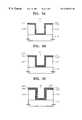
FIGS. 3A through 3E illustrate a fabrication method to still another embodiment of the present invention. Referring to FIG. 3A, anILD film 220 is formed on asemiconductor substrate 210 with a contact hole H3 throughILD 220 exposing a conductive region ofsemiconductor substrate 210. Anohmic layer 232 is formed of Ti on the exposed conductive region ofsemiconductor substrate 210, the side walls of contact hole H3 inILD film 220, and the upper surface ofILD film 220, and then abarrier layer 234 is formed of TiN onohmic layer 232. These layers can be formed in sequence by the same processes described above in reference to corresponding layers illustrated in FIGS. 1A and 1B.
Then, a firstinterface control layer 242, as a thin Al film containing Si, is formed onbarrier layer 234, to a thickness on the order of several angstroms to several tens of angstroms, preferably, less than 10 Å. Again, the same method described with reference to FIG. 1C for forminginterface control layer 42 can form firstinterface control layer 242.
Referring to FIG. 3B, a secondinterface control layer 244, which is formed of Cu, is formed on firstinterface control layer 242 by the same method as described with reference to FIG.2A. Alternatively, secondinterface control layer 244 may also be formed of Ti, W, Si, Ta or Ag, instead of Cu. In this embodiment, secondinterface control layer 244 is continuous thin layers as described above. However, secondinterface control layer 244 may include multiple separated islands on firstinterface control layer 242. Such islands can be formed by using a mask to limit formation of secondinterface control layer 244 to specific areas. Alternatively, selective etching can pattern a continuous layer.
Referring to FIG. 3C, a hydrogen-containing gas or nitrogen-containing gas is supplied to the surface ofinterface control layer 244 to form a thinsurface treatment layer 246 oninterface control layer 244 in the same way that was described with reference to FIGS. 1D and 2B.Surface treatment layer 246 helps prevent oxidation ofinterface control layer 244, for example, when moving the semiconductor structure to another processing apparatus.
Referring to FIG. 3D, a CVD blanket deposition of Al fills contact hole H3 and formsconductive layer 250 onsurface treatment layer 246. When the CVD blanket deposition is performed in-situ after forminginterface control layer 244, formingsurface treatment layer 246 may be omitted. Like the previously described methods, interface control layers242 and244 promote uniform Al grain nucleation and prevents Al agglomeration in the CVD blanket deposition, so thatconductive layer 250 can have a uniform surface morphology.
Referring to FIG. 3E, an annealing ofconductive layer 250 forms anAl interconnection layer 250adoped with Cu by promoting a diffusion of Cu atoms from secondinterface control layer 244 intoconductive layer 250. The annealing is performed at about 300 to 500° C., preferably, about 450 to 480° C. The doping ofAl interconnection layer 250aimproves reliability ofAl interconnection layer 250a.
As described above, an interface control layer formed according to the present invention promotes a uniform deposition of an interconnection layer which is formed on the interface control layer, so that the interconnection layer can have a uniform surface morphology. In addition, the interface control layer can act as a dopant of the interconnection layer, thereby improving reliability of the interconnection layer.
Although the invention has been described with reference to particular embodiments, the description is only an example of the inventor's application and should not be taken as a limitation. Various adaptations and combinations of features of the embodiments disclosed are within the scope of the invention as defined by the following claims.
Claims (25)
1. A semiconductor device fabrication method comprising:
(a) forming an interlayer dielectric (ILD) film having a contact hole, the contact hole exposing a conductive region of an underlying structure;
(b) forming an interface control layer of a plurality of atomic layers continuously deposited on inner walls of the contact hole and an upper surface of the interlayer dielectric film; and
(c) forming a contact plug in the contact hole and an interconnection layer on the inferface control layer by depositing aluminum in the contact hole and on the interface control layer.
2. The method ofclaim 1 , wherein after step (a) and before step (b), the method further comprises:
forming an ohmic layer on the inner walls of the contact hole and on the upper surface of the interlayer dielectric film; and
forming a barrier layer on the ohmic layer,
wherein the interface control layer is formed on the barrier layer.
3. The method ofclaim 2 , wherein the interface control layer is an aluminum (Al) layer containing silicon (Si).
4. The method ofclaim 3 , wherein atomic layer deposition (ALD) forms the interface control layer.
5. The method ofclaim 4 , wherein step (b) comprises:
(b1) flowing a Si-containing gas on the barrier layer, so that Si atoms are adsorbed to the barrier layer;
(b2) removing excess Si-containing gas from around the barrier layer;
(b3) flowing an Al-containing gas on the barrier layer to which the Si atoms were adsorbed, so that Al atoms are adsorbed to the barrier layer;
(b4) removing excess Al-containing gas from around the barrier layer; and
(b5) repeating steps (b1) through (b4) to form the Al layer containing Si on the barrier layer.
6. The method ofclaim 5 , wherein the barrier layer is a titanium (Ti)-rich titanium nitride (TiN) layer.
7. The method ofclaim 5 , wherein hydrogen (H2) gas is supplied together with the Al-containing gas in step (b3) to facilitate deposition of Al atoms.
8. The method ofclaim 1 , further comprising annealing the semiconductor device after step (c), so that the interconnection layer is doped with metal atoms from the interface control layer.
9. The method ofclaim 8 , wherein after step (a) and before step (b), the method further comprises:
forming an ohmic layer on the inner walls of the contact hole and on the upper surface of the interlayer dielectric film; and
forming a barrier layer on the ohmic layer,
wherein the interface control layer is formed on the barrier layer in step (b).
10. The method ofclaim 9 , wherein the interface control layer is formed of a material selected from a group consisting of copper (Cu), titanium (Ti), tungsten (W), silicon (Si), tantalum (Ta), and silver (Ag).
11. The method ofclaim 10 , wherein a method selected from a group consisting of atomic layer deposition (ALD), cyclic CVD, and digital CVD forms the interface control layer.
12. The method ofclaim 11 , wherein the interface control layer is formed of Ti, and step (b) comprises flowing a gas selected from a group consisting of TiCl4, tridiethylamine titanate, tridimethylamine titanate, and combinations thereof.
13. The method ofclaim 11 , wherein the interface control layer is formed of W, and step (b) comprises flowing WF6gas.
14. The method ofclaim 11 , wherein the interface control layer is formed of Si, and step (b) comprises flowing a gas selected from a group consisting of SiH3Cl, SiH2Cl2, SiHCl3, Si2H6or SiCl4and combinations thereof.
15. The method ofclaim 10 , wherein the interface control layer is formed of Cu, and step (b) comprises:
(b1) flowing a source gas selected from a group consisting of (hexafluoroacetyl)copper(trimethylvinylsilane), CuCl2, Cu2l4, and combinations thereof so that Cu atoms are adsorbed to the barrier layer;
(b2) purging the source gas from around the semiconductor device after step (b1); and
(b3) repeating steps (b1) and (b2).
16. The methodclaim 1 , further comprising annealing the semiconductor device after step (c) so that the interconnection layer is doped with metal atoms from the interface control layer, and step (b) comprises:
(b′) forming a first interface control layer as an Al film containing Si and a plurality of atomic layers on the inner wall of the contact hole and the upper surface of the interlayer dielectric film; and
(b″) forming a second interface control layer having a plurality of atomic layers continuously deposited on the first interface control layer.
17. The method ofclaim 16 , wherein after step (a) and before step (b), the method further comprises:
forming an ohmic layer on the inner walls of the contact hole and on the upper surface of the interlayer dielectric film; and
forming a barrier layer on the ohmic layer,
wherein the first interface control layer is formed on the barrier layer.
18. The method ofclaim 17 , wherein atomic layer deposition (ALD) forms the first and second interface control layers.
19. The method ofclaim 18 , wherein step (b′) comprises:
(b′1) applying a Si-containing gas to the barrier layer so that Si atoms are adsorbed to the barrier layer;
(b′2) removing excess Si-containing gas from around the semiconductor device;
(b′3) applying an Al-containing gas to the barrier layer to which the Si atoms are adsorbed, so that Al atoms are adsorbed to the barrier layer;
(b′4) removing excess Al-containing gas from around the semiconductor device; and
(b′5) repeating steps (b′1) through (b′4) to form the Al film containing Si on the barrier layer.
20. The method ofclaim 19 , wherein hydrogen (H2) gas is applied together with the Al-containing gas in step (b′3).
21. The method ofclaim 18 , wherein the second interface control layer is formed of a material selected from a group consisting of copper (Cu), titanium (Ti), tungsten (W), silicon (Si), tantalum (Ta) and silver (Ag).
22. The method ofclaim 21 , wherein the second interface control layer is formed of Cu, and step (b″) comprises:
(b″1) applying a gas selected from a group consisting of (hexafluoroacetyl)copper(trimethylvinylsilane) ) [(hfac)Cu(TMVS)], CuCl2, Cu2l4, and combinations thereof so that Cu atoms are adsorbed to the barrier layer;
(b″2) purging from around the semiconductor device after step (b″1); and
(b″3) repeating steps (b″1) and (b″2).
23. The method ofclaim 1 , wherein step (c) is performed in-situ after step (b).
24. The method ofclaim 1 , wherein after step (b) and before step (c), the method further comprises forming a surface treatment layer on the interface control layer, the surface treatment layer preventing oxidation of the surface of the interface control layer, wherein Al deposition in step (c) is performed on the surface treatment layer.
25. The method ofclaim 24 , wherein the surface treatment layer is formed by adsorbing hydrogen or nitrogen to the interface control layer.
Applications Claiming Priority (2)
| Application Number | Priority Date | Filing Date | Title |
|---|---|---|---|
| KR98-38413 | 1998-09-17 | ||
| KR1019980038413AKR100287180B1 (en) | 1998-09-17 | 1998-09-17 | Method for manufacturing semiconductor device including metal interconnection formed using interface control layer |
Publications (2)
| Publication Number | Publication Date |
|---|---|
| US20010029094A1 US20010029094A1 (en) | 2001-10-11 |
| US6358829B2true US6358829B2 (en) | 2002-03-19 |
Family
ID=19550907
Family Applications (1)
| Application Number | Title | Priority Date | Filing Date |
|---|---|---|---|
| US09/397,616Expired - LifetimeUS6358829B2 (en) | 1998-09-17 | 1999-09-16 | Semiconductor device fabrication method using an interface control layer to improve a metal interconnection layer |
Country Status (3)
| Country | Link |
|---|---|
| US (1) | US6358829B2 (en) |
| JP (1) | JP4005738B2 (en) |
| KR (1) | KR100287180B1 (en) |
Cited By (157)
| Publication number | Priority date | Publication date | Assignee | Title |
|---|---|---|---|---|
| US20020036780A1 (en)* | 2000-09-27 | 2002-03-28 | Hiroaki Nakamura | Image processing apparatus |
| US20020173094A1 (en)* | 2001-05-18 | 2002-11-21 | Youngjin Park | Contact plug formation for devices with stacked capacitors |
| US20020197863A1 (en)* | 2001-06-20 | 2002-12-26 | Mak Alfred W. | System and method to form a composite film stack utilizing sequential deposition techniques |
| WO2002103774A1 (en)* | 2001-06-15 | 2002-12-27 | Applied Materials, Inc. | Intergrated barrier layer structure for copper contact level metallization |
| US20030013300A1 (en)* | 2001-07-16 | 2003-01-16 | Applied Materials, Inc. | Method and apparatus for depositing tungsten after surface treatment to improve film characteristics |
| US20030059538A1 (en)* | 2001-09-26 | 2003-03-27 | Applied Materials, Inc. | Integration of barrier layer and seed layer |
| US20030082301A1 (en)* | 2001-10-26 | 2003-05-01 | Applied Materials, Inc. | Enhanced copper growth with ultrathin barrier layer for high performance interconnects |
| US6559472B2 (en)* | 2000-11-21 | 2003-05-06 | Micron Technology, Inc. | Film composition |
| US20030104126A1 (en)* | 2001-10-10 | 2003-06-05 | Hongbin Fang | Method for depositing refractory metal layers employing sequential deposition techniques |
| US20030106490A1 (en)* | 2001-12-06 | 2003-06-12 | Applied Materials, Inc. | Apparatus and method for fast-cycle atomic layer deposition |
| US20030108674A1 (en)* | 2001-12-07 | 2003-06-12 | Applied Materials, Inc. | Cyclical deposition of refractory metal silicon nitride |
| US20030127043A1 (en)* | 2001-07-13 | 2003-07-10 | Applied Materials, Inc. | Pulsed nucleation deposition of tungsten layers |
| US20030129308A1 (en)* | 2001-11-16 | 2003-07-10 | Applied Materials, Inc. | Atomic layer deposition of copper using a reducing gas and non-fluorinated copper precursors |
| US6592942B1 (en)* | 2000-07-07 | 2003-07-15 | Asm International N.V. | Method for vapour deposition of a film onto a substrate |
| US20030153181A1 (en)* | 2002-02-11 | 2003-08-14 | Applied Materials, Inc. | Deposition of tungsten films |
| US20030161952A1 (en)* | 2002-02-26 | 2003-08-28 | Applied Materials, Inc. | Cyclical deposition of tungsten nitride for metal oxide gate electrode |
| US20030172872A1 (en)* | 2002-01-25 | 2003-09-18 | Applied Materials, Inc. | Apparatus for cyclical deposition of thin films |
| US20030186561A1 (en)* | 2002-03-26 | 2003-10-02 | Applied Materials, Inc. | Deposition of film layers |
| US20030190497A1 (en)* | 2002-04-08 | 2003-10-09 | Applied Materials, Inc. | Cyclical deposition of a variable content titanium silicon nitride layer |
| US20030189208A1 (en)* | 2002-04-05 | 2003-10-09 | Kam Law | Deposition of silicon layers for active matrix liquid crystal display (AMLCD) applications |
| US20030190423A1 (en)* | 2002-04-08 | 2003-10-09 | Applied Materials, Inc. | Multiple precursor cyclical deposition system |
| US6638810B2 (en) | 2000-02-22 | 2003-10-28 | Applied Materials, Inc. | Tantalum nitride CVD deposition by tantalum oxide densification |
| US20030219540A1 (en)* | 2000-08-28 | 2003-11-27 | Law Kam S. | Pre-polycoating of glass substrates |
| US20030224600A1 (en)* | 2002-03-04 | 2003-12-04 | Wei Cao | Sequential deposition of tantalum nitride using a tantalum-containing precursor and a nitrogen-containing precursor |
| US20030224578A1 (en)* | 2001-12-21 | 2003-12-04 | Hua Chung | Selective deposition of a barrier layer on a dielectric material |
| US6664192B2 (en) | 1999-08-24 | 2003-12-16 | Interuniversitair Microelektronica Centrum (Imec) | Method for bottomless deposition of barrier layers in integrated circuit metallization schemes |
| US20030232497A1 (en)* | 2002-04-16 | 2003-12-18 | Ming Xi | System and method for forming an integrated barrier layer |
| US20030235961A1 (en)* | 2002-04-17 | 2003-12-25 | Applied Materials, Inc. | Cyclical sequential deposition of multicomponent films |
| US20040009665A1 (en)* | 2002-06-04 | 2004-01-15 | Applied Materials, Inc. | Deposition of copper films |
| US20040011404A1 (en)* | 2002-07-19 | 2004-01-22 | Ku Vincent W | Valve design and configuration for fast delivery system |
| US20040014315A1 (en)* | 2001-07-16 | 2004-01-22 | Applied Materials, Inc. | Formation of composite tungsten films |
| US20040013803A1 (en)* | 2002-07-16 | 2004-01-22 | Applied Materials, Inc. | Formation of titanium nitride films using a cyclical deposition process |
| US20040015300A1 (en)* | 2002-07-22 | 2004-01-22 | Seshadri Ganguli | Method and apparatus for monitoring solid precursor delivery |
| US20040018304A1 (en)* | 2002-07-10 | 2004-01-29 | Applied Materials, Inc. | Method of film deposition using activated precursor gases |
| US20040018723A1 (en)* | 2000-06-27 | 2004-01-29 | Applied Materials, Inc. | Formation of boride barrier layers using chemisorption techniques |
| US6686271B2 (en) | 2000-05-15 | 2004-02-03 | Asm International N.V. | Protective layers prior to alternating layer deposition |
| US20040048451A1 (en)* | 2001-06-21 | 2004-03-11 | Marsh Eugene P. | Rhodium film and method of formation |
| US6718126B2 (en) | 2001-09-14 | 2004-04-06 | Applied Materials, Inc. | Apparatus and method for vaporizing solid precursor for CVD or atomic layer deposition |
| US20040065255A1 (en)* | 2002-10-02 | 2004-04-08 | Applied Materials, Inc. | Cyclical layer deposition system |
| US20040071897A1 (en)* | 2002-10-11 | 2004-04-15 | Applied Materials, Inc. | Activated species generator for rapid cycle deposition processes |
| US20040077183A1 (en)* | 2002-06-04 | 2004-04-22 | Hua Chung | Titanium tantalum nitride silicide layer |
| US6727169B1 (en) | 1999-10-15 | 2004-04-27 | Asm International, N.V. | Method of making conformal lining layers for damascene metallization |
| US6753248B1 (en) | 2003-01-27 | 2004-06-22 | Applied Materials, Inc. | Post metal barrier/adhesion film |
| US20040126682A1 (en)* | 2002-09-16 | 2004-07-01 | Dreher Martin Leonhard | Print control for flexographic printing |
| US6759325B2 (en)* | 2000-05-15 | 2004-07-06 | Asm Microchemistry Oy | Sealing porous structures |
| US20040144311A1 (en)* | 2002-11-14 | 2004-07-29 | Ling Chen | Apparatus and method for hybrid chemical processing |
| US20040198069A1 (en)* | 2003-04-04 | 2004-10-07 | Applied Materials, Inc. | Method for hafnium nitride deposition |
| US20040197492A1 (en)* | 2001-05-07 | 2004-10-07 | Applied Materials, Inc. | CVD TiSiN barrier for copper integration |
| US20040209465A1 (en)* | 2000-06-28 | 2004-10-21 | Applied Materials, Inc. | Method and apparatus for depositing refractory metal layers employing sequential deposition techniques to form a nucleation layer |
| US6809026B2 (en) | 2001-12-21 | 2004-10-26 | Applied Materials, Inc. | Selective deposition of a barrier layer on a metal film |
| US20040224089A1 (en)* | 2002-10-18 | 2004-11-11 | Applied Materials, Inc. | Silicon-containing layer deposition with silicon compounds |
| US6818517B1 (en) | 2003-08-29 | 2004-11-16 | Asm International N.V. | Methods of depositing two or more layers on a substrate in situ |
| US6821563B2 (en) | 2002-10-02 | 2004-11-23 | Applied Materials, Inc. | Gas distribution system for cyclical layer deposition |
| US20040256351A1 (en)* | 2003-01-07 | 2004-12-23 | Hua Chung | Integration of ALD/CVD barriers with porous low k materials |
| US20050009325A1 (en)* | 2003-06-18 | 2005-01-13 | Hua Chung | Atomic layer deposition of barrier materials |
| US6855368B1 (en) | 2000-06-28 | 2005-02-15 | Applied Materials, Inc. | Method and system for controlling the presence of fluorine in refractory metal layers |
| US20050046028A1 (en)* | 2003-09-02 | 2005-03-03 | Jung Byung Hyun | Semiconductor device and method for fabricating the same |
| US20050062130A1 (en)* | 2003-09-23 | 2005-03-24 | Anthony Ciancio | Semiconductor device and making thereof |
| US20050067103A1 (en)* | 2003-09-26 | 2005-03-31 | Applied Materials, Inc. | Interferometer endpoint monitoring device |
| US20050079691A1 (en)* | 2003-10-10 | 2005-04-14 | Applied Materials, Inc. | Methods of selective deposition of heavily doped epitaxial SiGe |
| US20050106865A1 (en)* | 2001-09-26 | 2005-05-19 | Applied Materials, Inc. | Integration of ALD tantalum nitride for copper metallization |
| US6911391B2 (en) | 2002-01-26 | 2005-06-28 | Applied Materials, Inc. | Integration of titanium and titanium nitride layers |
| US20050139948A1 (en)* | 2001-09-26 | 2005-06-30 | Applied Materials, Inc. | Integration of barrier layer and seed layer |
| US6915592B2 (en) | 2002-07-29 | 2005-07-12 | Applied Materials, Inc. | Method and apparatus for generating gas to a processing chamber |
| US20050186765A1 (en)* | 2004-02-23 | 2005-08-25 | Yi Ma | Gate electrode dopant activation method for semiconductor manufacturing |
| US6955211B2 (en) | 2002-07-17 | 2005-10-18 | Applied Materials, Inc. | Method and apparatus for gas temperature control in a semiconductor processing system |
| US20050260357A1 (en)* | 2004-05-21 | 2005-11-24 | Applied Materials, Inc. | Stabilization of high-k dielectric materials |
| US20050271813A1 (en)* | 2004-05-12 | 2005-12-08 | Shreyas Kher | Apparatuses and methods for atomic layer deposition of hafnium-containing high-k dielectric materials |
| US20060006542A1 (en)* | 2004-07-09 | 2006-01-12 | Han-Choon Lee | Semiconductor device and method for manufacturing the same |
| US20060019033A1 (en)* | 2004-05-21 | 2006-01-26 | Applied Materials, Inc. | Plasma treatment of hafnium-containing materials |
| US20060019495A1 (en)* | 2004-07-20 | 2006-01-26 | Applied Materials, Inc. | Atomic layer deposition of tantalum-containing materials using the tantalum precursor taimata |
| US6998014B2 (en) | 2002-01-26 | 2006-02-14 | Applied Materials, Inc. | Apparatus and method for plasma assisted deposition |
| US20060062917A1 (en)* | 2004-05-21 | 2006-03-23 | Shankar Muthukrishnan | Vapor deposition of hafnium silicate materials with tris(dimethylamino)silane |
| US20060089007A1 (en)* | 1998-10-01 | 2006-04-27 | Applied Materials, Inc. | In situ deposition of a low K dielectric layer, barrier layer, etch stop, and anti-reflective coating for damascene application |
| US20060115934A1 (en)* | 2004-12-01 | 2006-06-01 | Yihwan Kim | Selective epitaxy process with alternating gas supply |
| US20060115933A1 (en)* | 2004-12-01 | 2006-06-01 | Applied Materials, Inc. | Use of CL2 and/or HCL during silicon epitaxial film formation |
| US20060128150A1 (en)* | 2004-12-10 | 2006-06-15 | Applied Materials, Inc. | Ruthenium as an underlayer for tungsten film deposition |
| US20060153995A1 (en)* | 2004-05-21 | 2006-07-13 | Applied Materials, Inc. | Method for fabricating a dielectric stack |
| US20060166414A1 (en)* | 2004-12-01 | 2006-07-27 | Carlson David K | Selective deposition |
| US20060169669A1 (en)* | 2005-01-31 | 2006-08-03 | Applied Materials, Inc. | Etchant treatment processes for substrate surfaces and chamber surfaces |
| US20060205194A1 (en)* | 2005-02-04 | 2006-09-14 | Matthias Bauer | Methods of depositing electrically active doped crystalline Si-containing films |
| US7132338B2 (en) | 2003-10-10 | 2006-11-07 | Applied Materials, Inc. | Methods to fabricate MOSFET devices using selective deposition process |
| US20060257295A1 (en)* | 2002-07-17 | 2006-11-16 | Ling Chen | Apparatus and method for generating a chemical precursor |
| US20060286774A1 (en)* | 2005-06-21 | 2006-12-21 | Applied Materials. Inc. | Method for forming silicon-containing materials during a photoexcitation deposition process |
| US20060286776A1 (en)* | 2005-06-21 | 2006-12-21 | Applied Materials, Inc. | Method for forming silicon-containing materials during a photoexcitation deposition process |
| US20070009658A1 (en)* | 2001-07-13 | 2007-01-11 | Yoo Jong H | Pulse nucleation enhanced nucleation technique for improved step coverage and better gap fill for WCVD process |
| US20070066023A1 (en)* | 2005-09-20 | 2007-03-22 | Randhir Thakur | Method to form a device on a soi substrate |
| US20070099422A1 (en)* | 2005-10-28 | 2007-05-03 | Kapila Wijekoon | Process for electroless copper deposition |
| US20070117359A1 (en)* | 2002-08-14 | 2007-05-24 | Asm America, Inc. | Deposition of amorphous silicon-containing films |
| US20070113868A1 (en)* | 2005-11-22 | 2007-05-24 | Applied Materials,Inc. | Apparatus and a method for cleaning a dielectric film |
| US20070128864A1 (en)* | 2005-11-04 | 2007-06-07 | Paul Ma | Apparatus and process for plasma-enhanced atomic layer deposition |
| US20070161216A1 (en)* | 2005-12-22 | 2007-07-12 | Matthias Bauer | Epitaxial deposition of doped semiconductor materials |
| US7262133B2 (en) | 2003-01-07 | 2007-08-28 | Applied Materials, Inc. | Enhancement of copper line reliability using thin ALD tan film to cap the copper line |
| US20070202254A1 (en)* | 2001-07-25 | 2007-08-30 | Seshadri Ganguli | Process for forming cobalt-containing materials |
| US20070207624A1 (en)* | 2006-03-02 | 2007-09-06 | Applied Materials, Inc. | Multiple nitrogen plasma treatments for thin SiON dielectrics |
| US20070259112A1 (en)* | 2006-04-07 | 2007-11-08 | Applied Materials, Inc. | Gas manifolds for use during epitaxial film formation |
| US20070287272A1 (en)* | 2006-06-07 | 2007-12-13 | Asm America, Inc. | Selective epitaxial formation of semiconductor films |
| US20080022924A1 (en)* | 2006-07-31 | 2008-01-31 | Applied Materials, Inc. | Methods of forming carbon-containing silicon epitaxial layers |
| US20080026549A1 (en)* | 2006-07-31 | 2008-01-31 | Applied Materials, Inc. | Methods of controlling morphology during epitaxial layer formation |
| US20080073645A1 (en)* | 2001-02-12 | 2008-03-27 | Asm America, Inc. | Thin films and methods of making them |
| US20080085611A1 (en)* | 2006-10-09 | 2008-04-10 | Amit Khandelwal | Deposition and densification process for titanium nitride barrier layers |
| US20080096380A1 (en)* | 2006-10-24 | 2008-04-24 | Chung-Chi Ko | Low-k interconnect structures with reduced RC delay |
| US20080099436A1 (en)* | 2006-10-30 | 2008-05-01 | Michael Grimbergen | Endpoint detection for photomask etching |
| US20080135914A1 (en)* | 2006-06-30 | 2008-06-12 | Krishna Nety M | Nanocrystal formation |
| US20080176149A1 (en)* | 2006-10-30 | 2008-07-24 | Applied Materials, Inc. | Endpoint detection for photomask etching |
| US7405158B2 (en) | 2000-06-28 | 2008-07-29 | Applied Materials, Inc. | Methods for depositing tungsten layers employing atomic layer deposition techniques |
| US7416979B2 (en) | 2001-07-25 | 2008-08-26 | Applied Materials, Inc. | Deposition methods for barrier and tungsten materials |
| US20080268635A1 (en)* | 2001-07-25 | 2008-10-30 | Sang-Ho Yu | Process for forming cobalt and cobalt silicide materials in copper contact applications |
| US20090053426A1 (en)* | 2001-07-25 | 2009-02-26 | Jiang Lu | Cobalt deposition on barrier surfaces |
| US20090075029A1 (en)* | 2007-09-19 | 2009-03-19 | Asm America, Inc. | Stressor for engineered strain on channel |
| US20090081868A1 (en)* | 2007-09-25 | 2009-03-26 | Applied Materials, Inc. | Vapor deposition processes for tantalum carbide nitride materials |
| US20090078916A1 (en)* | 2007-09-25 | 2009-03-26 | Applied Materials, Inc. | Tantalum carbide nitride materials by vapor deposition processes |
| US20090087585A1 (en)* | 2007-09-28 | 2009-04-02 | Wei Ti Lee | Deposition processes for titanium nitride barrier and aluminum |
| US20090111246A1 (en)* | 2007-10-26 | 2009-04-30 | Asm America, Inc. | Inhibitors for selective deposition of silicon containing films |
| US20090163001A1 (en)* | 2007-12-21 | 2009-06-25 | Asm America, Inc. | Separate injection of reactive species in selective formation of films |
| US20090215260A1 (en)* | 2008-02-21 | 2009-08-27 | Chong Jiang | Methods of forming a barrier layer in an interconnect structure |
| US20090227105A1 (en)* | 2008-03-04 | 2009-09-10 | Xinyu Fu | Methods of forming a layer for barrier applications in an interconnect structure |
| US7611990B2 (en) | 2001-07-25 | 2009-11-03 | Applied Materials, Inc. | Deposition methods for barrier and tungsten materials |
| US7648927B2 (en) | 2005-06-21 | 2010-01-19 | Applied Materials, Inc. | Method for forming silicon-containing materials during a photoexcitation deposition process |
| US20100022099A1 (en)* | 2005-03-15 | 2010-01-28 | Asm America, Inc. | Method of forming non-conformal layers |
| US7659158B2 (en) | 2008-03-31 | 2010-02-09 | Applied Materials, Inc. | Atomic layer deposition processes for non-volatile memory devices |
| US20100062614A1 (en)* | 2008-09-08 | 2010-03-11 | Ma Paul F | In-situ chamber treatment and deposition process |
| US20100062181A1 (en)* | 2002-02-05 | 2010-03-11 | Canon Anelva Corporation | Metal film production apparatus and metal film production method |
| US20100112215A1 (en)* | 2008-10-31 | 2010-05-06 | Applied Materials, Inc. | Chemical precursor ampoule for vapor deposition processes |
| US7732327B2 (en) | 2000-06-28 | 2010-06-08 | Applied Materials, Inc. | Vapor deposition of tungsten materials |
| US20100151676A1 (en)* | 2008-12-16 | 2010-06-17 | Applied Materials, Inc. | Densification process for titanium nitride layer for submicron applications |
| US7780785B2 (en) | 2001-10-26 | 2010-08-24 | Applied Materials, Inc. | Gas delivery apparatus for atomic layer deposition |
| US7798096B2 (en) | 2006-05-05 | 2010-09-21 | Applied Materials, Inc. | Plasma, UV and ion/neutral assisted ALD or CVD in a batch tool |
| US20100255658A1 (en)* | 2009-04-07 | 2010-10-07 | Asm America, Inc. | Substrate reactor with adjustable injectors for mixing gases within reaction chamber |
| US20100317177A1 (en)* | 2003-10-10 | 2010-12-16 | Applied Materials, Inc. | Methods for forming silicon germanium layers |
| US20110117732A1 (en)* | 2009-11-17 | 2011-05-19 | Asm America, Inc. | Cyclical epitaxial deposition and etch |
| US7964505B2 (en) | 2005-01-19 | 2011-06-21 | Applied Materials, Inc. | Atomic layer deposition of tungsten materials |
| US8187970B2 (en) | 2001-07-25 | 2012-05-29 | Applied Materials, Inc. | Process for forming cobalt and cobalt silicide materials in tungsten contact applications |
| US8586479B2 (en) | 2012-01-23 | 2013-11-19 | Applied Materials, Inc. | Methods for forming a contact metal layer in semiconductor devices |
| US8642473B2 (en) | 2011-03-04 | 2014-02-04 | Applied Materials, Inc. | Methods for contact clean |
| US8809170B2 (en) | 2011-05-19 | 2014-08-19 | Asm America Inc. | High throughput cyclical epitaxial deposition and etch process |
| US8912096B2 (en) | 2011-04-28 | 2014-12-16 | Applied Materials, Inc. | Methods for precleaning a substrate prior to metal silicide fabrication process |
| US8927423B2 (en) | 2011-12-16 | 2015-01-06 | Applied Materials, Inc. | Methods for annealing a contact metal layer to form a metal silicidation layer |
| US9018108B2 (en) | 2013-01-25 | 2015-04-28 | Applied Materials, Inc. | Low shrinkage dielectric films |
| US9218961B2 (en) | 2011-09-19 | 2015-12-22 | Applied Materials, Inc. | Methods of forming a metal containing layer on a substrate with high uniformity and good profile control |
| US9330939B2 (en) | 2012-03-28 | 2016-05-03 | Applied Materials, Inc. | Method of enabling seamless cobalt gap-fill |
| US9418890B2 (en) | 2008-09-08 | 2016-08-16 | Applied Materials, Inc. | Method for tuning a deposition rate during an atomic layer deposition process |
| US9508561B2 (en) | 2014-03-11 | 2016-11-29 | Applied Materials, Inc. | Methods for forming interconnection structures in an integrated cluster system for semicondcutor applications |
| US9528185B2 (en) | 2014-08-22 | 2016-12-27 | Applied Materials, Inc. | Plasma uniformity control by arrays of unit cell plasmas |
| US9543163B2 (en) | 2013-08-20 | 2017-01-10 | Applied Materials, Inc. | Methods for forming features in a material layer utilizing a combination of a main etching and a cyclical etching process |
| US9685371B2 (en) | 2013-09-27 | 2017-06-20 | Applied Materials, Inc. | Method of enabling seamless cobalt gap-fill |
| US11361978B2 (en) | 2018-07-25 | 2022-06-14 | Applied Materials, Inc. | Gas delivery module |
| US11462417B2 (en) | 2017-08-18 | 2022-10-04 | Applied Materials, Inc. | High pressure and high temperature anneal chamber |
| US11527421B2 (en) | 2017-11-11 | 2022-12-13 | Micromaterials, LLC | Gas delivery system for high pressure processing chamber |
| US11581183B2 (en) | 2018-05-08 | 2023-02-14 | Applied Materials, Inc. | Methods of forming amorphous carbon hard mask layers and hard mask layers formed therefrom |
| US11610773B2 (en) | 2017-11-17 | 2023-03-21 | Applied Materials, Inc. | Condenser system for high pressure processing system |
| US11694912B2 (en) | 2017-08-18 | 2023-07-04 | Applied Materials, Inc. | High pressure and high temperature anneal chamber |
| US11705337B2 (en) | 2017-05-25 | 2023-07-18 | Applied Materials, Inc. | Tungsten defluorination by high pressure treatment |
| US11749555B2 (en) | 2018-12-07 | 2023-09-05 | Applied Materials, Inc. | Semiconductor processing system |
| US11881411B2 (en) | 2018-03-09 | 2024-01-23 | Applied Materials, Inc. | High pressure annealing process for metal containing materials |
| US11901222B2 (en) | 2020-02-17 | 2024-02-13 | Applied Materials, Inc. | Multi-step process for flowable gap-fill film |
| US12198951B2 (en) | 2017-03-10 | 2025-01-14 | Applied Materials, Inc. | High pressure wafer processing systems and related methods |
Families Citing this family (12)
| Publication number | Priority date | Publication date | Assignee | Title |
|---|---|---|---|---|
| KR100680940B1 (en)* | 2000-12-28 | 2007-02-08 | 주식회사 하이닉스반도체 | Metal wiring formation method of semiconductor device |
| US7422961B2 (en)* | 2003-03-14 | 2008-09-09 | Advanced Micro Devices, Inc. | Method of forming isolation regions for integrated circuits |
| US20040175926A1 (en)* | 2003-03-07 | 2004-09-09 | Advanced Micro Devices, Inc. | Method for manufacturing a semiconductor component having a barrier-lined opening |
| US7906393B2 (en)* | 2004-01-28 | 2011-03-15 | Micron Technology, Inc. | Methods for forming small-scale capacitor structures |
| JP2006339371A (en)* | 2005-06-01 | 2006-12-14 | Toshiba Corp | Manufacturing method of semiconductor device |
| JP5011355B2 (en)* | 2009-07-30 | 2012-08-29 | 東京エレクトロン株式会社 | Deposition method |
| US20120187505A1 (en)* | 2011-01-25 | 2012-07-26 | International Business Machines Corporation | Self-aligned III-V MOSFET fabrication with in-situ III-V epitaxy and in-situ metal epitaxy and contact formation |
| US20130243971A1 (en)* | 2012-03-14 | 2013-09-19 | Applied Materials, Inc. | Apparatus and Process for Atomic Layer Deposition with Horizontal Laser |
| CN107112278B (en)* | 2014-12-15 | 2021-05-04 | 应用材料公司 | Ultrathin Dielectric Diffusion Barriers and Etch Stop Layers for Advanced Interconnect Applications |
| KR102657866B1 (en)* | 2019-06-10 | 2024-04-17 | 에스케이하이닉스 주식회사 | Semiconductor device and method for fabricating the same |
| WO2021145077A1 (en)* | 2020-01-15 | 2021-07-22 | 東京エレクトロン株式会社 | Film forming method, film forming device, and method for manufacturing semiconductor device |
| CN116033739A (en)* | 2021-10-25 | 2023-04-28 | 长鑫存储技术有限公司 | Semiconductor structure and manufacturing method thereof |
Citations (2)
| Publication number | Priority date | Publication date | Assignee | Title |
|---|---|---|---|---|
| US5391517A (en)* | 1993-09-13 | 1995-02-21 | Motorola Inc. | Process for forming copper interconnect structure |
| US5552341A (en)* | 1992-12-10 | 1996-09-03 | Samsung Electronics Co., Ltd. | Semiconductor device and method for manufacturing the same |
Family Cites Families (1)
| Publication number | Priority date | Publication date | Assignee | Title |
|---|---|---|---|---|
| JP2616402B2 (en)* | 1993-10-18 | 1997-06-04 | 日本電気株式会社 | Method for manufacturing semiconductor device |
- 1998
- 1998-09-17KRKR1019980038413Apatent/KR100287180B1/ennot_activeExpired - Fee Related
- 1999
- 1999-03-04JPJP05700899Apatent/JP4005738B2/ennot_activeExpired - Fee Related
- 1999-09-16USUS09/397,616patent/US6358829B2/ennot_activeExpired - Lifetime
Patent Citations (2)
| Publication number | Priority date | Publication date | Assignee | Title |
|---|---|---|---|---|
| US5552341A (en)* | 1992-12-10 | 1996-09-03 | Samsung Electronics Co., Ltd. | Semiconductor device and method for manufacturing the same |
| US5391517A (en)* | 1993-09-13 | 1995-02-21 | Motorola Inc. | Process for forming copper interconnect structure |
Cited By (380)
| Publication number | Priority date | Publication date | Assignee | Title |
|---|---|---|---|---|
| US20090130837A1 (en)* | 1998-10-01 | 2009-05-21 | Applied Materials, Inc. | In situ deposition of a low k dielectric layer, barrier layer, etch stop, and anti-reflective coating for damascene application |
| US7470611B2 (en) | 1998-10-01 | 2008-12-30 | Applied Materials, Inc. | In situ deposition of a low K dielectric layer, barrier layer, etch stop, and anti-reflective coating for damascene application |
| US20060089007A1 (en)* | 1998-10-01 | 2006-04-27 | Applied Materials, Inc. | In situ deposition of a low K dielectric layer, barrier layer, etch stop, and anti-reflective coating for damascene application |
| US7670945B2 (en) | 1998-10-01 | 2010-03-02 | Applied Materials, Inc. | In situ deposition of a low κ dielectric layer, barrier layer, etch stop, and anti-reflective coating for damascene application |
| US6664192B2 (en) | 1999-08-24 | 2003-12-16 | Interuniversitair Microelektronica Centrum (Imec) | Method for bottomless deposition of barrier layers in integrated circuit metallization schemes |
| US20040121616A1 (en)* | 1999-08-24 | 2004-06-24 | Alessandra Satta | Method for bottomless deposition of barrier layers in integrated circuit metallization schemes |
| US6852635B2 (en) | 1999-08-24 | 2005-02-08 | Interuniversitair Nizroelecmica | Method for bottomless deposition of barrier layers in integrated circuit metallization schemes |
| US20040130029A1 (en)* | 1999-10-15 | 2004-07-08 | Ivo Raaijmakers | Conformal lining layers for damascene metallization |
| US6727169B1 (en) | 1999-10-15 | 2004-04-27 | Asm International, N.V. | Method of making conformal lining layers for damascene metallization |
| US7102235B2 (en) | 1999-10-15 | 2006-09-05 | Asm International N.V. | Conformal lining layers for damascene metallization |
| US20070096321A1 (en)* | 1999-10-15 | 2007-05-03 | Ivo Raaijmakers | Conformal lining layers for damascene metallization |
| US7670944B2 (en)* | 1999-10-15 | 2010-03-02 | Asm International N.V. | Conformal lining layers for damascene metallization |
| US6638810B2 (en) | 2000-02-22 | 2003-10-28 | Applied Materials, Inc. | Tantalum nitride CVD deposition by tantalum oxide densification |
| US6686271B2 (en) | 2000-05-15 | 2004-02-03 | Asm International N.V. | Protective layers prior to alternating layer deposition |
| US6699783B2 (en) | 2000-05-15 | 2004-03-02 | Asm International N.V. | Method for controlling conformality with alternating layer deposition |
| US6759325B2 (en)* | 2000-05-15 | 2004-07-06 | Asm Microchemistry Oy | Sealing porous structures |
| US7501344B2 (en) | 2000-06-27 | 2009-03-10 | Applied Materials, Inc. | Formation of boride barrier layers using chemisorption techniques |
| US7208413B2 (en) | 2000-06-27 | 2007-04-24 | Applied Materials, Inc. | Formation of boride barrier layers using chemisorption techniques |
| US7501343B2 (en) | 2000-06-27 | 2009-03-10 | Applied Materials, Inc. | Formation of boride barrier layers using chemisorption techniques |
| US20040018723A1 (en)* | 2000-06-27 | 2004-01-29 | Applied Materials, Inc. | Formation of boride barrier layers using chemisorption techniques |
| US6831004B2 (en) | 2000-06-27 | 2004-12-14 | Applied Materials, Inc. | Formation of boride barrier layers using chemisorption techniques |
| US7465666B2 (en) | 2000-06-28 | 2008-12-16 | Applied Materials, Inc. | Method for forming tungsten materials during vapor deposition processes |
| US20040209465A1 (en)* | 2000-06-28 | 2004-10-21 | Applied Materials, Inc. | Method and apparatus for depositing refractory metal layers employing sequential deposition techniques to form a nucleation layer |
| US7465665B2 (en) | 2000-06-28 | 2008-12-16 | Applied Materials, Inc. | Method for depositing tungsten-containing layers by vapor deposition techniques |
| US20060128132A1 (en)* | 2000-06-28 | 2006-06-15 | Applied Materials, Inc. | Method and system for controlling the presence of fluorine in refractory metal layers |
| US7033922B2 (en) | 2000-06-28 | 2006-04-25 | Applied Materials. Inc. | Method and system for controlling the presence of fluorine in refractory metal layers |
| US7220673B2 (en) | 2000-06-28 | 2007-05-22 | Applied Materials, Inc. | Method for depositing tungsten-containing layers by vapor deposition techniques |
| US7235486B2 (en) | 2000-06-28 | 2007-06-26 | Applied Materials, Inc. | Method for forming tungsten materials during vapor deposition processes |
| US7732327B2 (en) | 2000-06-28 | 2010-06-08 | Applied Materials, Inc. | Vapor deposition of tungsten materials |
| US6855368B1 (en) | 2000-06-28 | 2005-02-15 | Applied Materials, Inc. | Method and system for controlling the presence of fluorine in refractory metal layers |
| US7709385B2 (en) | 2000-06-28 | 2010-05-04 | Applied Materials, Inc. | Method for depositing tungsten-containing layers by vapor deposition techniques |
| US20050059241A1 (en)* | 2000-06-28 | 2005-03-17 | Moris Kori | Method and system for controlling the presence of fluorine in refractory metal layers |
| US7405158B2 (en) | 2000-06-28 | 2008-07-29 | Applied Materials, Inc. | Methods for depositing tungsten layers employing atomic layer deposition techniques |
| US7745333B2 (en) | 2000-06-28 | 2010-06-29 | Applied Materials, Inc. | Methods for depositing tungsten layers employing atomic layer deposition techniques |
| US20070218688A1 (en)* | 2000-06-28 | 2007-09-20 | Ming Xi | Method for depositing tungsten-containing layers by vapor deposition techniques |
| US7674715B2 (en) | 2000-06-28 | 2010-03-09 | Applied Materials, Inc. | Method for forming tungsten materials during vapor deposition processes |
| US20060264031A1 (en)* | 2000-06-28 | 2006-11-23 | Ming Xi | Method for depositing tungsten-containing layers by vapor deposition techniques |
| US7115494B2 (en) | 2000-06-28 | 2006-10-03 | Applied Materials, Inc. | Method and system for controlling the presence of fluorine in refractory metal layers |
| US7846840B2 (en) | 2000-06-28 | 2010-12-07 | Applied Materials, Inc. | Method for forming tungsten materials during vapor deposition processes |
| US6592942B1 (en)* | 2000-07-07 | 2003-07-15 | Asm International N.V. | Method for vapour deposition of a film onto a substrate |
| US20030219540A1 (en)* | 2000-08-28 | 2003-11-27 | Law Kam S. | Pre-polycoating of glass substrates |
| US20020036780A1 (en)* | 2000-09-27 | 2002-03-28 | Hiroaki Nakamura | Image processing apparatus |
| US6559472B2 (en)* | 2000-11-21 | 2003-05-06 | Micron Technology, Inc. | Film composition |
| US20080073645A1 (en)* | 2001-02-12 | 2008-03-27 | Asm America, Inc. | Thin films and methods of making them |
| US7893433B2 (en) | 2001-02-12 | 2011-02-22 | Asm America, Inc. | Thin films and methods of making them |
| US20100012030A1 (en)* | 2001-02-12 | 2010-01-21 | Asm America, Inc. | Process for Deposition of Semiconductor Films |
| US8360001B2 (en) | 2001-02-12 | 2013-01-29 | Asm America, Inc. | Process for deposition of semiconductor films |
| US20040197492A1 (en)* | 2001-05-07 | 2004-10-07 | Applied Materials, Inc. | CVD TiSiN barrier for copper integration |
| US6958296B2 (en) | 2001-05-07 | 2005-10-25 | Applied Materials, Inc. | CVD TiSiN barrier for copper integration |
| US6753252B2 (en)* | 2001-05-18 | 2004-06-22 | Infineon Technologies Ag | Contact plug formation for devices with stacked capacitors |
| US20020173094A1 (en)* | 2001-05-18 | 2002-11-21 | Youngjin Park | Contact plug formation for devices with stacked capacitors |
| WO2002103774A1 (en)* | 2001-06-15 | 2002-12-27 | Applied Materials, Inc. | Intergrated barrier layer structure for copper contact level metallization |
| US6849545B2 (en) | 2001-06-20 | 2005-02-01 | Applied Materials, Inc. | System and method to form a composite film stack utilizing sequential deposition techniques |
| US20020197863A1 (en)* | 2001-06-20 | 2002-12-26 | Mak Alfred W. | System and method to form a composite film stack utilizing sequential deposition techniques |
| US20040048451A1 (en)* | 2001-06-21 | 2004-03-11 | Marsh Eugene P. | Rhodium film and method of formation |
| US6943073B2 (en)* | 2001-06-21 | 2005-09-13 | Micron Technology, Inc. | Process for low temperature atomic layer deposition of RH |
| US20060160344A1 (en)* | 2001-06-21 | 2006-07-20 | Micron Technology, Inc. | Rhodium film and method of formation |
| US20070009658A1 (en)* | 2001-07-13 | 2007-01-11 | Yoo Jong H | Pulse nucleation enhanced nucleation technique for improved step coverage and better gap fill for WCVD process |
| US20030127043A1 (en)* | 2001-07-13 | 2003-07-10 | Applied Materials, Inc. | Pulsed nucleation deposition of tungsten layers |
| US7211144B2 (en) | 2001-07-13 | 2007-05-01 | Applied Materials, Inc. | Pulsed nucleation deposition of tungsten layers |
| US7695563B2 (en) | 2001-07-13 | 2010-04-13 | Applied Materials, Inc. | Pulsed deposition process for tungsten nucleation |
| US20050287807A1 (en)* | 2001-07-16 | 2005-12-29 | Applied Materials, Inc. | Formation of composite tungsten films |
| US20030013300A1 (en)* | 2001-07-16 | 2003-01-16 | Applied Materials, Inc. | Method and apparatus for depositing tungsten after surface treatment to improve film characteristics |
| US6939804B2 (en) | 2001-07-16 | 2005-09-06 | Applied Materials, Inc. | Formation of composite tungsten films |
| US6936538B2 (en) | 2001-07-16 | 2005-08-30 | Applied Materials, Inc. | Method and apparatus for depositing tungsten after surface treatment to improve film characteristics |
| US7238552B2 (en) | 2001-07-16 | 2007-07-03 | Applied Materials, Inc. | Method and apparatus for depositing tungsten after surface treatment to improve film characteristics |
| US7605083B2 (en) | 2001-07-16 | 2009-10-20 | Applied Materials, Inc. | Formation of composite tungsten films |
| US20040014315A1 (en)* | 2001-07-16 | 2004-01-22 | Applied Materials, Inc. | Formation of composite tungsten films |
| US7749815B2 (en) | 2001-07-16 | 2010-07-06 | Applied Materials, Inc. | Methods for depositing tungsten after surface treatment |
| US7384867B2 (en) | 2001-07-16 | 2008-06-10 | Applied Materials, Inc. | Formation of composite tungsten films |
| US20080268635A1 (en)* | 2001-07-25 | 2008-10-30 | Sang-Ho Yu | Process for forming cobalt and cobalt silicide materials in copper contact applications |
| US20090053426A1 (en)* | 2001-07-25 | 2009-02-26 | Jiang Lu | Cobalt deposition on barrier surfaces |
| US7611990B2 (en) | 2001-07-25 | 2009-11-03 | Applied Materials, Inc. | Deposition methods for barrier and tungsten materials |
| US9051641B2 (en) | 2001-07-25 | 2015-06-09 | Applied Materials, Inc. | Cobalt deposition on barrier surfaces |
| US7416979B2 (en) | 2001-07-25 | 2008-08-26 | Applied Materials, Inc. | Deposition methods for barrier and tungsten materials |
| US8110489B2 (en) | 2001-07-25 | 2012-02-07 | Applied Materials, Inc. | Process for forming cobalt-containing materials |
| US9209074B2 (en) | 2001-07-25 | 2015-12-08 | Applied Materials, Inc. | Cobalt deposition on barrier surfaces |
| US8563424B2 (en) | 2001-07-25 | 2013-10-22 | Applied Materials, Inc. | Process for forming cobalt and cobalt silicide materials in tungsten contact applications |
| US20070202254A1 (en)* | 2001-07-25 | 2007-08-30 | Seshadri Ganguli | Process for forming cobalt-containing materials |
| US8187970B2 (en) | 2001-07-25 | 2012-05-29 | Applied Materials, Inc. | Process for forming cobalt and cobalt silicide materials in tungsten contact applications |
| US20040170403A1 (en)* | 2001-09-14 | 2004-09-02 | Applied Materials, Inc. | Apparatus and method for vaporizing solid precursor for CVD or atomic layer deposition |
| US6718126B2 (en) | 2001-09-14 | 2004-04-06 | Applied Materials, Inc. | Apparatus and method for vaporizing solid precursor for CVD or atomic layer deposition |
| US7352048B2 (en) | 2001-09-26 | 2008-04-01 | Applied Materials, Inc. | Integration of barrier layer and seed layer |
| US20050106865A1 (en)* | 2001-09-26 | 2005-05-19 | Applied Materials, Inc. | Integration of ALD tantalum nitride for copper metallization |
| US20030059538A1 (en)* | 2001-09-26 | 2003-03-27 | Applied Materials, Inc. | Integration of barrier layer and seed layer |
| US20050139948A1 (en)* | 2001-09-26 | 2005-06-30 | Applied Materials, Inc. | Integration of barrier layer and seed layer |
| US7494908B2 (en) | 2001-09-26 | 2009-02-24 | Applied Materials, Inc. | Apparatus for integration of barrier layer and seed layer |
| US7049226B2 (en) | 2001-09-26 | 2006-05-23 | Applied Materials, Inc. | Integration of ALD tantalum nitride for copper metallization |
| US20030104126A1 (en)* | 2001-10-10 | 2003-06-05 | Hongbin Fang | Method for depositing refractory metal layers employing sequential deposition techniques |
| US20060040052A1 (en)* | 2001-10-10 | 2006-02-23 | Hongbin Fang | Methods for depositing tungsten layers employing atomic layer deposition techniques |
| US6797340B2 (en) | 2001-10-10 | 2004-09-28 | Applied Materials, Inc. | Method for depositing refractory metal layers employing sequential deposition techniques |
| US20040247788A1 (en)* | 2001-10-10 | 2004-12-09 | Hongbin Fang | Method for depositing refractory metal layers employing sequential deposition techniques |
| US8668776B2 (en) | 2001-10-26 | 2014-03-11 | Applied Materials, Inc. | Gas delivery apparatus and method for atomic layer deposition |
| US20030082301A1 (en)* | 2001-10-26 | 2003-05-01 | Applied Materials, Inc. | Enhanced copper growth with ultrathin barrier layer for high performance interconnects |
| US20030082307A1 (en)* | 2001-10-26 | 2003-05-01 | Applied Materials, Inc. | Integration of ALD tantalum nitride and alpha-phase tantalum for copper metallization application |
| US7780785B2 (en) | 2001-10-26 | 2010-08-24 | Applied Materials, Inc. | Gas delivery apparatus for atomic layer deposition |
| US6916398B2 (en) | 2001-10-26 | 2005-07-12 | Applied Materials, Inc. | Gas delivery apparatus and method for atomic layer deposition |
| US7780788B2 (en) | 2001-10-26 | 2010-08-24 | Applied Materials, Inc. | Gas delivery apparatus for atomic layer deposition |
| US20030079686A1 (en)* | 2001-10-26 | 2003-05-01 | Ling Chen | Gas delivery apparatus and method for atomic layer deposition |
| US20030124262A1 (en)* | 2001-10-26 | 2003-07-03 | Ling Chen | Integration of ALD tantalum nitride and alpha-phase tantalum for copper metallization application |
| US8318266B2 (en) | 2001-10-26 | 2012-11-27 | Applied Materials, Inc. | Enhanced copper growth with ultrathin barrier layer for high performance interconnects |
| US20070003698A1 (en)* | 2001-10-26 | 2007-01-04 | Ling Chen | Enhanced copper growth with ultrathin barrier layer for high performance interconnects |
| US8293328B2 (en) | 2001-10-26 | 2012-10-23 | Applied Materials, Inc. | Enhanced copper growth with ultrathin barrier layer for high performance interconnects |
| US6821891B2 (en) | 2001-11-16 | 2004-11-23 | Applied Materials, Inc. | Atomic layer deposition of copper using a reducing gas and non-fluorinated copper precursors |
| US20030129308A1 (en)* | 2001-11-16 | 2003-07-10 | Applied Materials, Inc. | Atomic layer deposition of copper using a reducing gas and non-fluorinated copper precursors |
| US20030106490A1 (en)* | 2001-12-06 | 2003-06-12 | Applied Materials, Inc. | Apparatus and method for fast-cycle atomic layer deposition |
| US6773507B2 (en) | 2001-12-06 | 2004-08-10 | Applied Materials, Inc. | Apparatus and method for fast-cycle atomic layer deposition |
| US20060216928A1 (en)* | 2001-12-07 | 2006-09-28 | Hua Chung | Cyclical deposition of refractory metal silicon nitride |
| US7892602B2 (en) | 2001-12-07 | 2011-02-22 | Applied Materials, Inc. | Cyclical deposition of refractory metal silicon nitride |
| US7081271B2 (en) | 2001-12-07 | 2006-07-25 | Applied Materials, Inc. | Cyclical deposition of refractory metal silicon nitride |
| US20030108674A1 (en)* | 2001-12-07 | 2003-06-12 | Applied Materials, Inc. | Cyclical deposition of refractory metal silicon nitride |
| US20030224578A1 (en)* | 2001-12-21 | 2003-12-04 | Hua Chung | Selective deposition of a barrier layer on a dielectric material |
| US6809026B2 (en) | 2001-12-21 | 2004-10-26 | Applied Materials, Inc. | Selective deposition of a barrier layer on a metal film |
| US6939801B2 (en) | 2001-12-21 | 2005-09-06 | Applied Materials, Inc. | Selective deposition of a barrier layer on a dielectric material |
| US7175713B2 (en) | 2002-01-25 | 2007-02-13 | Applied Materials, Inc. | Apparatus for cyclical deposition of thin films |
| US20030172872A1 (en)* | 2002-01-25 | 2003-09-18 | Applied Materials, Inc. | Apparatus for cyclical deposition of thin films |
| US20070095285A1 (en)* | 2002-01-25 | 2007-05-03 | Thakur Randhir P | Apparatus for cyclical depositing of thin films |
| US20090056626A1 (en)* | 2002-01-25 | 2009-03-05 | Applied Materials, Inc. | Apparatus for cyclical depositing of thin films |
| US8123860B2 (en) | 2002-01-25 | 2012-02-28 | Applied Materials, Inc. | Apparatus for cyclical depositing of thin films |
| US6998014B2 (en) | 2002-01-26 | 2006-02-14 | Applied Materials, Inc. | Apparatus and method for plasma assisted deposition |
| US7473638B2 (en) | 2002-01-26 | 2009-01-06 | Applied Materials, Inc. | Plasma-enhanced cyclic layer deposition process for barrier layers |
| US6911391B2 (en) | 2002-01-26 | 2005-06-28 | Applied Materials, Inc. | Integration of titanium and titanium nitride layers |
| US7732325B2 (en) | 2002-01-26 | 2010-06-08 | Applied Materials, Inc. | Plasma-enhanced cyclic layer deposition process for barrier layers |
| US7779784B2 (en) | 2002-01-26 | 2010-08-24 | Applied Materials, Inc. | Apparatus and method for plasma assisted deposition |
| US20060075966A1 (en)* | 2002-01-26 | 2006-04-13 | Applied Materials, Inc. | Apparatus and method for plasma assisted deposition |
| US7094685B2 (en) | 2002-01-26 | 2006-08-22 | Applied Materials, Inc. | Integration of titanium and titanium nitride layers |
| US20100062181A1 (en)* | 2002-02-05 | 2010-03-11 | Canon Anelva Corporation | Metal film production apparatus and metal film production method |
| US6827978B2 (en) | 2002-02-11 | 2004-12-07 | Applied Materials, Inc. | Deposition of tungsten films |
| US20030153181A1 (en)* | 2002-02-11 | 2003-08-14 | Applied Materials, Inc. | Deposition of tungsten films |
| US20070020924A1 (en)* | 2002-02-26 | 2007-01-25 | Shulin Wang | Tungsten nitride atomic layer deposition processes |
| US6833161B2 (en) | 2002-02-26 | 2004-12-21 | Applied Materials, Inc. | Cyclical deposition of tungsten nitride for metal oxide gate electrode |
| US20030161952A1 (en)* | 2002-02-26 | 2003-08-28 | Applied Materials, Inc. | Cyclical deposition of tungsten nitride for metal oxide gate electrode |
| US7745329B2 (en) | 2002-02-26 | 2010-06-29 | Applied Materials, Inc. | Tungsten nitride atomic layer deposition processes |
| US20050176240A1 (en)* | 2002-02-26 | 2005-08-11 | Shulin Wang | Cyclical deposition of tungsten nitride for metal oxide gate electrode |
| US7115499B2 (en) | 2002-02-26 | 2006-10-03 | Applied Materials, Inc. | Cyclical deposition of tungsten nitride for metal oxide gate electrode |
| US7429516B2 (en) | 2002-02-26 | 2008-09-30 | Applied Materials, Inc. | Tungsten nitride atomic layer deposition processes |
| US20060019494A1 (en)* | 2002-03-04 | 2006-01-26 | Wei Cao | Sequential deposition of tantalum nitride using a tantalum-containing precursor and a nitrogen-containing precursor |
| US7514358B2 (en) | 2002-03-04 | 2009-04-07 | Applied Materials, Inc. | Sequential deposition of tantalum nitride using a tantalum-containing precursor and a nitrogen-containing precursor |
| US20030224600A1 (en)* | 2002-03-04 | 2003-12-04 | Wei Cao | Sequential deposition of tantalum nitride using a tantalum-containing precursor and a nitrogen-containing precursor |
| US20110070730A1 (en)* | 2002-03-04 | 2011-03-24 | Wei Cao | Sequential deposition of tantalum nitride using a tantalum-containing precursor and a nitrogen-containing precursor |
| US6972267B2 (en) | 2002-03-04 | 2005-12-06 | Applied Materials, Inc. | Sequential deposition of tantalum nitride using a tantalum-containing precursor and a nitrogen-containing precursor |
| US7867896B2 (en) | 2002-03-04 | 2011-01-11 | Applied Materials, Inc. | Sequential deposition of tantalum nitride using a tantalum-containing precursor and a nitrogen-containing precursor |
| US6825134B2 (en) | 2002-03-26 | 2004-11-30 | Applied Materials, Inc. | Deposition of film layers by alternately pulsing a precursor and high frequency power in a continuous gas flow |
| US20030186561A1 (en)* | 2002-03-26 | 2003-10-02 | Applied Materials, Inc. | Deposition of film layers |
| US20030189208A1 (en)* | 2002-04-05 | 2003-10-09 | Kam Law | Deposition of silicon layers for active matrix liquid crystal display (AMLCD) applications |
| US7439191B2 (en) | 2002-04-05 | 2008-10-21 | Applied Materials, Inc. | Deposition of silicon layers for active matrix liquid crystal display (AMLCD) applications |
| US20030190423A1 (en)* | 2002-04-08 | 2003-10-09 | Applied Materials, Inc. | Multiple precursor cyclical deposition system |
| US6846516B2 (en) | 2002-04-08 | 2005-01-25 | Applied Materials, Inc. | Multiple precursor cyclical deposition system |
| US6720027B2 (en) | 2002-04-08 | 2004-04-13 | Applied Materials, Inc. | Cyclical deposition of a variable content titanium silicon nitride layer |
| US20030190497A1 (en)* | 2002-04-08 | 2003-10-09 | Applied Materials, Inc. | Cyclical deposition of a variable content titanium silicon nitride layer |
| US7867914B2 (en) | 2002-04-16 | 2011-01-11 | Applied Materials, Inc. | System and method for forming an integrated barrier layer |
| US20080014352A1 (en)* | 2002-04-16 | 2008-01-17 | Ming Xi | System and method for forming an integrated barrier layer |
| US7279432B2 (en) | 2002-04-16 | 2007-10-09 | Applied Materials, Inc. | System and method for forming an integrated barrier layer |
| US20030232497A1 (en)* | 2002-04-16 | 2003-12-18 | Ming Xi | System and method for forming an integrated barrier layer |
| US20030235961A1 (en)* | 2002-04-17 | 2003-12-25 | Applied Materials, Inc. | Cyclical sequential deposition of multicomponent films |
| US20040009665A1 (en)* | 2002-06-04 | 2004-01-15 | Applied Materials, Inc. | Deposition of copper films |
| US20040077183A1 (en)* | 2002-06-04 | 2004-04-22 | Hua Chung | Titanium tantalum nitride silicide layer |
| US7041335B2 (en) | 2002-06-04 | 2006-05-09 | Applied Materials, Inc. | Titanium tantalum nitride silicide layer |
| US20040018304A1 (en)* | 2002-07-10 | 2004-01-29 | Applied Materials, Inc. | Method of film deposition using activated precursor gases |
| US6838125B2 (en) | 2002-07-10 | 2005-01-04 | Applied Materials, Inc. | Method of film deposition using activated precursor gases |
| US20040013803A1 (en)* | 2002-07-16 | 2004-01-22 | Applied Materials, Inc. | Formation of titanium nitride films using a cyclical deposition process |
| US7588736B2 (en) | 2002-07-17 | 2009-09-15 | Applied Materials, Inc. | Apparatus and method for generating a chemical precursor |
| US20090011129A1 (en)* | 2002-07-17 | 2009-01-08 | Seshadri Ganguli | Method and apparatus for providing precursor gas to a processing chamber |
| US7429361B2 (en) | 2002-07-17 | 2008-09-30 | Applied Materials, Inc. | Method and apparatus for providing precursor gas to a processing chamber |
| US7569191B2 (en) | 2002-07-17 | 2009-08-04 | Applied Materials, Inc. | Method and apparatus for providing precursor gas to a processing chamber |
| US7678194B2 (en) | 2002-07-17 | 2010-03-16 | Applied Materials, Inc. | Method for providing gas to a processing chamber |
| US6955211B2 (en) | 2002-07-17 | 2005-10-18 | Applied Materials, Inc. | Method and apparatus for gas temperature control in a semiconductor processing system |
| US20060257295A1 (en)* | 2002-07-17 | 2006-11-16 | Ling Chen | Apparatus and method for generating a chemical precursor |
| US20070110898A1 (en)* | 2002-07-17 | 2007-05-17 | Seshadri Ganguli | Method and apparatus for providing precursor gas to a processing chamber |
| US20060213558A1 (en)* | 2002-07-19 | 2006-09-28 | Applied Materials, Inc. | Valve design and configuration for fast delivery system |
| US20040011404A1 (en)* | 2002-07-19 | 2004-01-22 | Ku Vincent W | Valve design and configuration for fast delivery system |
| US7066194B2 (en) | 2002-07-19 | 2006-06-27 | Applied Materials, Inc. | Valve design and configuration for fast delivery system |
| US20060213557A1 (en)* | 2002-07-19 | 2006-09-28 | Ku Vincent W | Valve design and configuration for fast delivery system |
| US7228873B2 (en) | 2002-07-19 | 2007-06-12 | Applied Materials, Inc. | Valve design and configuration for fast delivery system |
| US6772072B2 (en) | 2002-07-22 | 2004-08-03 | Applied Materials, Inc. | Method and apparatus for monitoring solid precursor delivery |
| US20040015300A1 (en)* | 2002-07-22 | 2004-01-22 | Seshadri Ganguli | Method and apparatus for monitoring solid precursor delivery |
| US7294208B2 (en) | 2002-07-29 | 2007-11-13 | Applied Materials, Inc. | Apparatus for providing gas to a processing chamber |
| US20050257735A1 (en)* | 2002-07-29 | 2005-11-24 | Guenther Rolf A | Method and apparatus for providing gas to a processing chamber |
| US6915592B2 (en) | 2002-07-29 | 2005-07-12 | Applied Materials, Inc. | Method and apparatus for generating gas to a processing chamber |
| US20070117359A1 (en)* | 2002-08-14 | 2007-05-24 | Asm America, Inc. | Deposition of amorphous silicon-containing films |
| US8921205B2 (en) | 2002-08-14 | 2014-12-30 | Asm America, Inc. | Deposition of amorphous silicon-containing films |
| US20040126682A1 (en)* | 2002-09-16 | 2004-07-01 | Dreher Martin Leonhard | Print control for flexographic printing |
| US20040065255A1 (en)* | 2002-10-02 | 2004-04-08 | Applied Materials, Inc. | Cyclical layer deposition system |
| US6821563B2 (en) | 2002-10-02 | 2004-11-23 | Applied Materials, Inc. | Gas distribution system for cyclical layer deposition |
| US6905737B2 (en) | 2002-10-11 | 2005-06-14 | Applied Materials, Inc. | Method of delivering activated species for rapid cyclical deposition |
| US20060035025A1 (en)* | 2002-10-11 | 2006-02-16 | Applied Materials, Inc. | Activated species generator for rapid cycle deposition processes |
| US20040071897A1 (en)* | 2002-10-11 | 2004-04-15 | Applied Materials, Inc. | Activated species generator for rapid cycle deposition processes |
| US20070240632A1 (en)* | 2002-10-18 | 2007-10-18 | Singh Kaushal K | Silicon-containing layer deposition with silicon compounds |
| US7540920B2 (en) | 2002-10-18 | 2009-06-02 | Applied Materials, Inc. | Silicon-containing layer deposition with silicon compounds |
| US7758697B2 (en) | 2002-10-18 | 2010-07-20 | Applied Materials, Inc. | Silicon-containing layer deposition with silicon compounds |
| US7645339B2 (en) | 2002-10-18 | 2010-01-12 | Applied Materials, Inc. | Silicon-containing layer deposition with silicon compounds |
| US20040224089A1 (en)* | 2002-10-18 | 2004-11-11 | Applied Materials, Inc. | Silicon-containing layer deposition with silicon compounds |
| US7204886B2 (en) | 2002-11-14 | 2007-04-17 | Applied Materials, Inc. | Apparatus and method for hybrid chemical processing |
| US7591907B2 (en) | 2002-11-14 | 2009-09-22 | Applied Materials, Inc. | Apparatus for hybrid chemical processing |
| US20070151514A1 (en)* | 2002-11-14 | 2007-07-05 | Ling Chen | Apparatus and method for hybrid chemical processing |
| US7402210B2 (en) | 2002-11-14 | 2008-07-22 | Applied Materials, Inc. | Apparatus and method for hybrid chemical processing |
| US20040144311A1 (en)* | 2002-11-14 | 2004-07-29 | Ling Chen | Apparatus and method for hybrid chemical processing |
| US20040256351A1 (en)* | 2003-01-07 | 2004-12-23 | Hua Chung | Integration of ALD/CVD barriers with porous low k materials |
| US7262133B2 (en) | 2003-01-07 | 2007-08-28 | Applied Materials, Inc. | Enhancement of copper line reliability using thin ALD tan film to cap the copper line |
| US7244683B2 (en) | 2003-01-07 | 2007-07-17 | Applied Materials, Inc. | Integration of ALD/CVD barriers with porous low k materials |
| US6753248B1 (en) | 2003-01-27 | 2004-06-22 | Applied Materials, Inc. | Post metal barrier/adhesion film |
| US7547952B2 (en) | 2003-04-04 | 2009-06-16 | Applied Materials, Inc. | Method for hafnium nitride deposition |
| US20040198069A1 (en)* | 2003-04-04 | 2004-10-07 | Applied Materials, Inc. | Method for hafnium nitride deposition |
| US20070190780A1 (en)* | 2003-06-18 | 2007-08-16 | Applied Materials, Inc. | Atomic layer deposition of barrier materials |
| US20050009325A1 (en)* | 2003-06-18 | 2005-01-13 | Hua Chung | Atomic layer deposition of barrier materials |
| US7595263B2 (en) | 2003-06-18 | 2009-09-29 | Applied Materials, Inc. | Atomic layer deposition of barrier materials |
| US7211508B2 (en) | 2003-06-18 | 2007-05-01 | Applied Materials, Inc. | Atomic layer deposition of tantalum based barrier materials |
| US6818517B1 (en) | 2003-08-29 | 2004-11-16 | Asm International N.V. | Methods of depositing two or more layers on a substrate in situ |
| US20050046028A1 (en)* | 2003-09-02 | 2005-03-03 | Jung Byung Hyun | Semiconductor device and method for fabricating the same |
| US7259092B2 (en)* | 2003-09-02 | 2007-08-21 | Dongbu Electronics Co., Ltd. | Semiconductor device and method for fabricating the same |
| US20050062130A1 (en)* | 2003-09-23 | 2005-03-24 | Anthony Ciancio | Semiconductor device and making thereof |
| US7078785B2 (en) | 2003-09-23 | 2006-07-18 | Freescale Semiconductor, Inc. | Semiconductor device and making thereof |
| US20050067103A1 (en)* | 2003-09-26 | 2005-03-31 | Applied Materials, Inc. | Interferometer endpoint monitoring device |
| US20070023393A1 (en)* | 2003-09-26 | 2007-02-01 | Nguyen Khiem K | Interferometer endpoint monitoring device |
| US7682984B2 (en) | 2003-09-26 | 2010-03-23 | Applied Materials, Inc. | Interferometer endpoint monitoring device |
| US7737007B2 (en) | 2003-10-10 | 2010-06-15 | Applied Materials, Inc. | Methods to fabricate MOSFET devices using a selective deposition process |
| US7132338B2 (en) | 2003-10-10 | 2006-11-07 | Applied Materials, Inc. | Methods to fabricate MOSFET devices using selective deposition process |
| US20050079691A1 (en)* | 2003-10-10 | 2005-04-14 | Applied Materials, Inc. | Methods of selective deposition of heavily doped epitaxial SiGe |
| US20070082451A1 (en)* | 2003-10-10 | 2007-04-12 | Samoilov Arkadii V | Methods to fabricate mosfet devices using a selective deposition process |
| US20100317177A1 (en)* | 2003-10-10 | 2010-12-16 | Applied Materials, Inc. | Methods for forming silicon germanium layers |
| US7439142B2 (en) | 2003-10-10 | 2008-10-21 | Applied Materials, Inc. | Methods to fabricate MOSFET devices using a selective deposition process |
| US7166528B2 (en) | 2003-10-10 | 2007-01-23 | Applied Materials, Inc. | Methods of selective deposition of heavily doped epitaxial SiGe |
| US20060234488A1 (en)* | 2003-10-10 | 2006-10-19 | Yihwan Kim | METHODS OF SELECTIVE DEPOSITION OF HEAVILY DOPED EPITAXIAL SiGe |
| US8501594B2 (en) | 2003-10-10 | 2013-08-06 | Applied Materials, Inc. | Methods for forming silicon germanium layers |
| US7517775B2 (en) | 2003-10-10 | 2009-04-14 | Applied Materials, Inc. | Methods of selective deposition of heavily doped epitaxial SiGe |
| US20050186765A1 (en)* | 2004-02-23 | 2005-08-25 | Yi Ma | Gate electrode dopant activation method for semiconductor manufacturing |
| US7611976B2 (en) | 2004-02-23 | 2009-11-03 | Applied Materials, Inc. | Gate electrode dopant activation method for semiconductor manufacturing |
| US7078302B2 (en) | 2004-02-23 | 2006-07-18 | Applied Materials, Inc. | Gate electrode dopant activation method for semiconductor manufacturing including a laser anneal |
| US20060286763A1 (en)* | 2004-02-23 | 2006-12-21 | Yi Ma | Gate electrode dopant activation method for semiconductor manufacturing |
| US20050271813A1 (en)* | 2004-05-12 | 2005-12-08 | Shreyas Kher | Apparatuses and methods for atomic layer deposition of hafnium-containing high-k dielectric materials |
| US7794544B2 (en) | 2004-05-12 | 2010-09-14 | Applied Materials, Inc. | Control of gas flow and delivery to suppress the formation of particles in an MOCVD/ALD system |
| US8343279B2 (en) | 2004-05-12 | 2013-01-01 | Applied Materials, Inc. | Apparatuses for atomic layer deposition |
| US8282992B2 (en) | 2004-05-12 | 2012-10-09 | Applied Materials, Inc. | Methods for atomic layer deposition of hafnium-containing high-K dielectric materials |
| US20060062917A1 (en)* | 2004-05-21 | 2006-03-23 | Shankar Muthukrishnan | Vapor deposition of hafnium silicate materials with tris(dimethylamino)silane |
| US20060153995A1 (en)* | 2004-05-21 | 2006-07-13 | Applied Materials, Inc. | Method for fabricating a dielectric stack |
| US20050260357A1 (en)* | 2004-05-21 | 2005-11-24 | Applied Materials, Inc. | Stabilization of high-k dielectric materials |
| US20060019033A1 (en)* | 2004-05-21 | 2006-01-26 | Applied Materials, Inc. | Plasma treatment of hafnium-containing materials |
| US8323754B2 (en) | 2004-05-21 | 2012-12-04 | Applied Materials, Inc. | Stabilization of high-k dielectric materials |
| US7407881B2 (en) | 2004-07-09 | 2008-08-05 | Dongbu Electronics Co., Ltd. | Semiconductor device and method for manufacturing the same |
| US20080277790A1 (en)* | 2004-07-09 | 2008-11-13 | Han-Choon Lee | Semiconductor Device |
| US20060006542A1 (en)* | 2004-07-09 | 2006-01-12 | Han-Choon Lee | Semiconductor device and method for manufacturing the same |
| US20090202710A1 (en)* | 2004-07-20 | 2009-08-13 | Christophe Marcadal | Atomic layer deposition of tantalum-containing materials using the tantalum precursor taimata |
| US20060019495A1 (en)* | 2004-07-20 | 2006-01-26 | Applied Materials, Inc. | Atomic layer deposition of tantalum-containing materials using the tantalum precursor taimata |
| US7691742B2 (en) | 2004-07-20 | 2010-04-06 | Applied Materials, Inc. | Atomic layer deposition of tantalum-containing materials using the tantalum precursor TAIMATA |
| US7241686B2 (en) | 2004-07-20 | 2007-07-10 | Applied Materials, Inc. | Atomic layer deposition of tantalum-containing materials using the tantalum precursor TAIMATA |
| US20070207596A1 (en)* | 2004-12-01 | 2007-09-06 | Yihwan Kim | Selective epitaxy process with alternating gas supply |
| US20060166414A1 (en)* | 2004-12-01 | 2006-07-27 | Carlson David K | Selective deposition |
| US7521365B2 (en) | 2004-12-01 | 2009-04-21 | Applied Materials, Inc. | Selective epitaxy process with alternating gas supply |
| US20110230036A1 (en)* | 2004-12-01 | 2011-09-22 | Applied Materials, Inc. | Use of cl2 and/or hcl during silicon epitaxial film formation |
| US20060260538A1 (en)* | 2004-12-01 | 2006-11-23 | Applied Materials, Inc. | Use of Cl2 and/or HCl during silicon epitaxial film formation |
| US7682940B2 (en) | 2004-12-01 | 2010-03-23 | Applied Materials, Inc. | Use of Cl2 and/or HCl during silicon epitaxial film formation |
| US7960256B2 (en) | 2004-12-01 | 2011-06-14 | Applied Materials, Inc. | Use of CL2 and/or HCL during silicon epitaxial film formation |
| US20060216876A1 (en)* | 2004-12-01 | 2006-09-28 | Yihwan Kim | Selective epitaxy process with alternating gas supply |
| US20060115933A1 (en)* | 2004-12-01 | 2006-06-01 | Applied Materials, Inc. | Use of CL2 and/or HCL during silicon epitaxial film formation |
| US7312128B2 (en) | 2004-12-01 | 2007-12-25 | Applied Materials, Inc. | Selective epitaxy process with alternating gas supply |
| US20060115934A1 (en)* | 2004-12-01 | 2006-06-01 | Yihwan Kim | Selective epitaxy process with alternating gas supply |
| US8586456B2 (en) | 2004-12-01 | 2013-11-19 | Applied Materials, Inc. | Use of CL2 and/or HCL during silicon epitaxial film formation |
| US7572715B2 (en) | 2004-12-01 | 2009-08-11 | Applied Materials, Inc. | Selective epitaxy process with alternating gas supply |
| US7732305B2 (en) | 2004-12-01 | 2010-06-08 | Applied Materials, Inc. | Use of Cl2 and/or HCl during silicon epitaxial film formation |
| US7560352B2 (en) | 2004-12-01 | 2009-07-14 | Applied Materials, Inc. | Selective deposition |
| US7429402B2 (en) | 2004-12-10 | 2008-09-30 | Applied Materials, Inc. | Ruthenium as an underlayer for tungsten film deposition |
| US20060128150A1 (en)* | 2004-12-10 | 2006-06-15 | Applied Materials, Inc. | Ruthenium as an underlayer for tungsten film deposition |
| US7964505B2 (en) | 2005-01-19 | 2011-06-21 | Applied Materials, Inc. | Atomic layer deposition of tungsten materials |
| US20060169669A1 (en)* | 2005-01-31 | 2006-08-03 | Applied Materials, Inc. | Etchant treatment processes for substrate surfaces and chamber surfaces |
| US20070224830A1 (en)* | 2005-01-31 | 2007-09-27 | Samoilov Arkadii V | Low temperature etchant for treatment of silicon-containing surfaces |
| US8445389B2 (en) | 2005-01-31 | 2013-05-21 | Applied Materials, Inc. | Etchant treatment processes for substrate surfaces and chamber surfaces |
| US8492284B2 (en) | 2005-01-31 | 2013-07-23 | Applied Materials, Inc. | Low temperature etchant for treatment of silicon-containing surfaces |
| US8093154B2 (en) | 2005-01-31 | 2012-01-10 | Applied Materials, Inc. | Etchant treatment processes for substrate surfaces and chamber surfaces |
| US7235492B2 (en) | 2005-01-31 | 2007-06-26 | Applied Materials, Inc. | Low temperature etchant for treatment of silicon-containing surfaces |
| US7648690B2 (en) | 2005-02-04 | 2010-01-19 | Asm America Inc. | Methods of making substitutionally carbon-doped crystalline Si-containing materials by chemical vapor deposition |
| US20060240630A1 (en)* | 2005-02-04 | 2006-10-26 | Matthias Bauer | Methods of making substitutionally carbon-doped crystalline Si-containing materials by chemical vapor deposition |
| US20060234504A1 (en)* | 2005-02-04 | 2006-10-19 | Matthias Bauer | Selective deposition of silicon-containing films |
| US7816236B2 (en) | 2005-02-04 | 2010-10-19 | Asm America Inc. | Selective deposition of silicon-containing films |
| US7687383B2 (en) | 2005-02-04 | 2010-03-30 | Asm America, Inc. | Methods of depositing electrically active doped crystalline Si-containing films |
| US20060205194A1 (en)* | 2005-02-04 | 2006-09-14 | Matthias Bauer | Methods of depositing electrically active doped crystalline Si-containing films |
| US7438760B2 (en) | 2005-02-04 | 2008-10-21 | Asm America, Inc. | Methods of making substitutionally carbon-doped crystalline Si-containing materials by chemical vapor deposition |
| US20100140744A1 (en)* | 2005-02-04 | 2010-06-10 | Asm America, Inc. | Methods of depositing electrically active doped crystalline si-containing films |
| US9190515B2 (en) | 2005-02-04 | 2015-11-17 | Asm America, Inc. | Structure comprises an As-deposited doped single crystalline Si-containing film |
| US8334218B2 (en) | 2005-03-15 | 2012-12-18 | Asm America, Inc. | Method of forming non-conformal layers |
| US20100022099A1 (en)* | 2005-03-15 | 2010-01-28 | Asm America, Inc. | Method of forming non-conformal layers |
| US7651955B2 (en) | 2005-06-21 | 2010-01-26 | Applied Materials, Inc. | Method for forming silicon-containing materials during a photoexcitation deposition process |
| US20100018460A1 (en)* | 2005-06-21 | 2010-01-28 | Applied Materials, Inc. | Method for forming silicon-containing materials during a photoexcitation deposition process |
| US7648927B2 (en) | 2005-06-21 | 2010-01-19 | Applied Materials, Inc. | Method for forming silicon-containing materials during a photoexcitation deposition process |
| US8387557B2 (en) | 2005-06-21 | 2013-03-05 | Applied Materials | Method for forming silicon-containing materials during a photoexcitation deposition process |
| US20060286776A1 (en)* | 2005-06-21 | 2006-12-21 | Applied Materials, Inc. | Method for forming silicon-containing materials during a photoexcitation deposition process |
| US20060286774A1 (en)* | 2005-06-21 | 2006-12-21 | Applied Materials. Inc. | Method for forming silicon-containing materials during a photoexcitation deposition process |
| US20070066023A1 (en)* | 2005-09-20 | 2007-03-22 | Randhir Thakur | Method to form a device on a soi substrate |
| US20070099422A1 (en)* | 2005-10-28 | 2007-05-03 | Kapila Wijekoon | Process for electroless copper deposition |
| US20070128864A1 (en)* | 2005-11-04 | 2007-06-07 | Paul Ma | Apparatus and process for plasma-enhanced atomic layer deposition |
| US9032906B2 (en) | 2005-11-04 | 2015-05-19 | Applied Materials, Inc. | Apparatus and process for plasma-enhanced atomic layer deposition |
| US7682946B2 (en) | 2005-11-04 | 2010-03-23 | Applied Materials, Inc. | Apparatus and process for plasma-enhanced atomic layer deposition |
| US20080268171A1 (en)* | 2005-11-04 | 2008-10-30 | Paul Ma | Apparatus and process for plasma-enhanced atomic layer deposition |
| US7850779B2 (en) | 2005-11-04 | 2010-12-14 | Applied Materisals, Inc. | Apparatus and process for plasma-enhanced atomic layer deposition |
| US7658802B2 (en) | 2005-11-22 | 2010-02-09 | Applied Materials, Inc. | Apparatus and a method for cleaning a dielectric film |
| US20070113868A1 (en)* | 2005-11-22 | 2007-05-24 | Applied Materials,Inc. | Apparatus and a method for cleaning a dielectric film |
| US20070161216A1 (en)* | 2005-12-22 | 2007-07-12 | Matthias Bauer | Epitaxial deposition of doped semiconductor materials |
| US7863163B2 (en) | 2005-12-22 | 2011-01-04 | Asm America, Inc. | Epitaxial deposition of doped semiconductor materials |
| US20070207624A1 (en)* | 2006-03-02 | 2007-09-06 | Applied Materials, Inc. | Multiple nitrogen plasma treatments for thin SiON dielectrics |
| US7674337B2 (en) | 2006-04-07 | 2010-03-09 | Applied Materials, Inc. | Gas manifolds for use during epitaxial film formation |
| US20070259112A1 (en)* | 2006-04-07 | 2007-11-08 | Applied Materials, Inc. | Gas manifolds for use during epitaxial film formation |
| US7798096B2 (en) | 2006-05-05 | 2010-09-21 | Applied Materials, Inc. | Plasma, UV and ion/neutral assisted ALD or CVD in a batch tool |
| US20070287272A1 (en)* | 2006-06-07 | 2007-12-13 | Asm America, Inc. | Selective epitaxial formation of semiconductor films |
| US8278176B2 (en) | 2006-06-07 | 2012-10-02 | Asm America, Inc. | Selective epitaxial formation of semiconductor films |
| US9312131B2 (en) | 2006-06-07 | 2016-04-12 | Asm America, Inc. | Selective epitaxial formation of semiconductive films |
| US20080135914A1 (en)* | 2006-06-30 | 2008-06-12 | Krishna Nety M | Nanocrystal formation |
| US20080026549A1 (en)* | 2006-07-31 | 2008-01-31 | Applied Materials, Inc. | Methods of controlling morphology during epitaxial layer formation |
| US7588980B2 (en) | 2006-07-31 | 2009-09-15 | Applied Materials, Inc. | Methods of controlling morphology during epitaxial layer formation |
| US20080022924A1 (en)* | 2006-07-31 | 2008-01-31 | Applied Materials, Inc. | Methods of forming carbon-containing silicon epitaxial layers |
| US8029620B2 (en) | 2006-07-31 | 2011-10-04 | Applied Materials, Inc. | Methods of forming carbon-containing silicon epitaxial layers |
| US20090280640A1 (en)* | 2006-10-09 | 2009-11-12 | Applied Materials Incorporated | Deposition and densification process for titanium nitride barrier layers |
| US7838441B2 (en) | 2006-10-09 | 2010-11-23 | Applied Materials, Inc. | Deposition and densification process for titanium nitride barrier layers |
| US20080085611A1 (en)* | 2006-10-09 | 2008-04-10 | Amit Khandelwal | Deposition and densification process for titanium nitride barrier layers |
| US7521379B2 (en) | 2006-10-09 | 2009-04-21 | Applied Materials, Inc. | Deposition and densification process for titanium nitride barrier layers |
| US9087877B2 (en)* | 2006-10-24 | 2015-07-21 | Taiwan Semiconductor Manufacturing Company, Ltd. | Low-k interconnect structures with reduced RC delay |
| US20080096380A1 (en)* | 2006-10-24 | 2008-04-24 | Chung-Chi Ko | Low-k interconnect structures with reduced RC delay |
| US8158526B2 (en) | 2006-10-30 | 2012-04-17 | Applied Materials, Inc. | Endpoint detection for photomask etching |
| US20080176149A1 (en)* | 2006-10-30 | 2008-07-24 | Applied Materials, Inc. | Endpoint detection for photomask etching |
| US8092695B2 (en) | 2006-10-30 | 2012-01-10 | Applied Materials, Inc. | Endpoint detection for photomask etching |
| US20080099436A1 (en)* | 2006-10-30 | 2008-05-01 | Michael Grimbergen | Endpoint detection for photomask etching |
| US20090014409A1 (en)* | 2006-10-30 | 2009-01-15 | Michael Grimbergen | Endpoint detection for photomask etching |
| US20090075029A1 (en)* | 2007-09-19 | 2009-03-19 | Asm America, Inc. | Stressor for engineered strain on channel |
| US7759199B2 (en) | 2007-09-19 | 2010-07-20 | Asm America, Inc. | Stressor for engineered strain on channel |
| US7585762B2 (en) | 2007-09-25 | 2009-09-08 | Applied Materials, Inc. | Vapor deposition processes for tantalum carbide nitride materials |
| US7678298B2 (en) | 2007-09-25 | 2010-03-16 | Applied Materials, Inc. | Tantalum carbide nitride materials by vapor deposition processes |
| US20090078916A1 (en)* | 2007-09-25 | 2009-03-26 | Applied Materials, Inc. | Tantalum carbide nitride materials by vapor deposition processes |
| US20090081868A1 (en)* | 2007-09-25 | 2009-03-26 | Applied Materials, Inc. | Vapor deposition processes for tantalum carbide nitride materials |
| US7824743B2 (en) | 2007-09-28 | 2010-11-02 | Applied Materials, Inc. | Deposition processes for titanium nitride barrier and aluminum |
| US20090087585A1 (en)* | 2007-09-28 | 2009-04-02 | Wei Ti Lee | Deposition processes for titanium nitride barrier and aluminum |
| US7939447B2 (en) | 2007-10-26 | 2011-05-10 | Asm America, Inc. | Inhibitors for selective deposition of silicon containing films |
| US20090111246A1 (en)* | 2007-10-26 | 2009-04-30 | Asm America, Inc. | Inhibitors for selective deposition of silicon containing films |
| US7655543B2 (en) | 2007-12-21 | 2010-02-02 | Asm America, Inc. | Separate injection of reactive species in selective formation of films |
| US7897491B2 (en) | 2007-12-21 | 2011-03-01 | Asm America, Inc. | Separate injection of reactive species in selective formation of films |
| US20090163001A1 (en)* | 2007-12-21 | 2009-06-25 | Asm America, Inc. | Separate injection of reactive species in selective formation of films |
| US20100093159A1 (en)* | 2007-12-21 | 2010-04-15 | Asm America, Inc. | Separate injection of reactive species in selective formation of films |
| US20090215260A1 (en)* | 2008-02-21 | 2009-08-27 | Chong Jiang | Methods of forming a barrier layer in an interconnect structure |
| US7767572B2 (en) | 2008-02-21 | 2010-08-03 | Applied Materials, Inc. | Methods of forming a barrier layer in an interconnect structure |
| US20090227105A1 (en)* | 2008-03-04 | 2009-09-10 | Xinyu Fu | Methods of forming a layer for barrier applications in an interconnect structure |
| US8168543B2 (en) | 2008-03-04 | 2012-05-01 | Applied Materials, Inc. | Methods of forming a layer for barrier applications in an interconnect structure |
| US7618893B2 (en) | 2008-03-04 | 2009-11-17 | Applied Materials, Inc. | Methods of forming a layer for barrier applications in an interconnect structure |
| US20100006425A1 (en)* | 2008-03-04 | 2010-01-14 | Xinyu Fu | Methods of forming a layer for barrier applications in an interconnect structure |
| US7659158B2 (en) | 2008-03-31 | 2010-02-09 | Applied Materials, Inc. | Atomic layer deposition processes for non-volatile memory devices |
| US8043907B2 (en) | 2008-03-31 | 2011-10-25 | Applied Materials, Inc. | Atomic layer deposition processes for non-volatile memory devices |
| US9418890B2 (en) | 2008-09-08 | 2016-08-16 | Applied Materials, Inc. | Method for tuning a deposition rate during an atomic layer deposition process |
| US8491967B2 (en) | 2008-09-08 | 2013-07-23 | Applied Materials, Inc. | In-situ chamber treatment and deposition process |
| US20100062614A1 (en)* | 2008-09-08 | 2010-03-11 | Ma Paul F | In-situ chamber treatment and deposition process |
| US20100112215A1 (en)* | 2008-10-31 | 2010-05-06 | Applied Materials, Inc. | Chemical precursor ampoule for vapor deposition processes |
| US8146896B2 (en) | 2008-10-31 | 2012-04-03 | Applied Materials, Inc. | Chemical precursor ampoule for vapor deposition processes |
| US20100151676A1 (en)* | 2008-12-16 | 2010-06-17 | Applied Materials, Inc. | Densification process for titanium nitride layer for submicron applications |
| US8486191B2 (en) | 2009-04-07 | 2013-07-16 | Asm America, Inc. | Substrate reactor with adjustable injectors for mixing gases within reaction chamber |
| US20100255658A1 (en)* | 2009-04-07 | 2010-10-07 | Asm America, Inc. | Substrate reactor with adjustable injectors for mixing gases within reaction chamber |
| US8367528B2 (en) | 2009-11-17 | 2013-02-05 | Asm America, Inc. | Cyclical epitaxial deposition and etch |
| US20110117732A1 (en)* | 2009-11-17 | 2011-05-19 | Asm America, Inc. | Cyclical epitaxial deposition and etch |
| US8642473B2 (en) | 2011-03-04 | 2014-02-04 | Applied Materials, Inc. | Methods for contact clean |
| US8912096B2 (en) | 2011-04-28 | 2014-12-16 | Applied Materials, Inc. | Methods for precleaning a substrate prior to metal silicide fabrication process |
| US8809170B2 (en) | 2011-05-19 | 2014-08-19 | Asm America Inc. | High throughput cyclical epitaxial deposition and etch process |
| US9218961B2 (en) | 2011-09-19 | 2015-12-22 | Applied Materials, Inc. | Methods of forming a metal containing layer on a substrate with high uniformity and good profile control |
| US8927423B2 (en) | 2011-12-16 | 2015-01-06 | Applied Materials, Inc. | Methods for annealing a contact metal layer to form a metal silicidation layer |
| US8586479B2 (en) | 2012-01-23 | 2013-11-19 | Applied Materials, Inc. | Methods for forming a contact metal layer in semiconductor devices |
| US10269633B2 (en) | 2012-03-28 | 2019-04-23 | Applied Materials, Inc. | Method of enabling seamless cobalt gap-fill |
| US9330939B2 (en) | 2012-03-28 | 2016-05-03 | Applied Materials, Inc. | Method of enabling seamless cobalt gap-fill |
| US9842769B2 (en) | 2012-03-28 | 2017-12-12 | Applied Materials, Inc. | Method of enabling seamless cobalt gap-fill |
| US9018108B2 (en) | 2013-01-25 | 2015-04-28 | Applied Materials, Inc. | Low shrinkage dielectric films |
| US9543163B2 (en) | 2013-08-20 | 2017-01-10 | Applied Materials, Inc. | Methods for forming features in a material layer utilizing a combination of a main etching and a cyclical etching process |
| US10699946B2 (en) | 2013-09-27 | 2020-06-30 | Applied Materials, Inc. | Method of enabling seamless cobalt gap-fill |
| US9685371B2 (en) | 2013-09-27 | 2017-06-20 | Applied Materials, Inc. | Method of enabling seamless cobalt gap-fill |
| US9508561B2 (en) | 2014-03-11 | 2016-11-29 | Applied Materials, Inc. | Methods for forming interconnection structures in an integrated cluster system for semicondcutor applications |
| US9528185B2 (en) | 2014-08-22 | 2016-12-27 | Applied Materials, Inc. | Plasma uniformity control by arrays of unit cell plasmas |
| US12198951B2 (en) | 2017-03-10 | 2025-01-14 | Applied Materials, Inc. | High pressure wafer processing systems and related methods |
| US11705337B2 (en) | 2017-05-25 | 2023-07-18 | Applied Materials, Inc. | Tungsten defluorination by high pressure treatment |
| US11462417B2 (en) | 2017-08-18 | 2022-10-04 | Applied Materials, Inc. | High pressure and high temperature anneal chamber |
| US11469113B2 (en) | 2017-08-18 | 2022-10-11 | Applied Materials, Inc. | High pressure and high temperature anneal chamber |
| US11694912B2 (en) | 2017-08-18 | 2023-07-04 | Applied Materials, Inc. | High pressure and high temperature anneal chamber |
| US11527421B2 (en) | 2017-11-11 | 2022-12-13 | Micromaterials, LLC | Gas delivery system for high pressure processing chamber |
| US11756803B2 (en) | 2017-11-11 | 2023-09-12 | Applied Materials, Inc. | Gas delivery system for high pressure processing chamber |
| US11610773B2 (en) | 2017-11-17 | 2023-03-21 | Applied Materials, Inc. | Condenser system for high pressure processing system |
| US11881411B2 (en) | 2018-03-09 | 2024-01-23 | Applied Materials, Inc. | High pressure annealing process for metal containing materials |
| US11581183B2 (en) | 2018-05-08 | 2023-02-14 | Applied Materials, Inc. | Methods of forming amorphous carbon hard mask layers and hard mask layers formed therefrom |
| US11361978B2 (en) | 2018-07-25 | 2022-06-14 | Applied Materials, Inc. | Gas delivery module |
| US11749555B2 (en) | 2018-12-07 | 2023-09-05 | Applied Materials, Inc. | Semiconductor processing system |
| US11901222B2 (en) | 2020-02-17 | 2024-02-13 | Applied Materials, Inc. | Multi-step process for flowable gap-fill film |
Also Published As
| Publication number | Publication date |
|---|---|
| KR100287180B1 (en) | 2001-04-16 |
| US20010029094A1 (en) | 2001-10-11 |
| JP4005738B2 (en) | 2007-11-14 |
| JP2000100753A (en) | 2000-04-07 |
| KR20000020013A (en) | 2000-04-15 |
Similar Documents
| Publication | Publication Date | Title |
|---|---|---|
| US6358829B2 (en) | Semiconductor device fabrication method using an interface control layer to improve a metal interconnection layer | |
| US6727169B1 (en) | Method of making conformal lining layers for damascene metallization | |
| US7955972B2 (en) | Methods for growing low-resistivity tungsten for high aspect ratio and small features | |
| JP4043785B2 (en) | Bottomless deposition method of barrier layer in integrated circuit metallization scheme | |
| US7244683B2 (en) | Integration of ALD/CVD barriers with porous low k materials | |
| EP1221177B1 (en) | Conformal lining layers for damascene metallization | |
| US8211799B2 (en) | Atomic layer deposition of tungsten materials | |
| US7405158B2 (en) | Methods for depositing tungsten layers employing atomic layer deposition techniques | |
| US20030124262A1 (en) | Integration of ALD tantalum nitride and alpha-phase tantalum for copper metallization application | |
| US20060292864A1 (en) | Plasma-enhanced cyclic layer deposition process for barrier layers | |
| JP7655948B2 (en) | Fluorine-free tungsten atomic layer deposition for improved dielectric selectivity | |
| KR100455382B1 (en) | Method for forming metal interconnections of semiconductor device having dual damascene structure | |
| JP4001509B2 (en) | Method for forming diffusion barrier film of semiconductor element | |
| JP4711624B2 (en) | Integration of ALD tantalum nitride and alpha phase tantalum for copper electrode formation applications | |
| US20020132469A1 (en) | Method for forming metal wiring layer | |
| JP2002057125A (en) | Method of forming metal wiring | |
| US20020072227A1 (en) | Method for improving barrier properties of refractory metals/metal nitrides with a safer alternative to silane | |
| JPH06268072A (en) | Formation of metal film |
Legal Events
| Date | Code | Title | Description |
|---|---|---|---|
| AS | Assignment | Owner name:SAMSUNG ELECTRONICS CO., LTD., KOREA, REPUBLIC OF Free format text:ASSIGNMENT OF ASSIGNORS INTEREST;ASSIGNORS:YOON, MEE-YOUNG;LEE, SANG-IN;LIM, HYUN-SEOK;REEL/FRAME:010260/0544;SIGNING DATES FROM 19990915 TO 19990916 | |
| STCF | Information on status: patent grant | Free format text:PATENTED CASE | |
| FPAY | Fee payment | Year of fee payment:4 | |
| FEPP | Fee payment procedure | Free format text:PAYOR NUMBER ASSIGNED (ORIGINAL EVENT CODE: ASPN); ENTITY STATUS OF PATENT OWNER: LARGE ENTITY | |
| FPAY | Fee payment | Year of fee payment:8 | |
| FPAY | Fee payment | Year of fee payment:12 |