US6358800B1 - Method of forming a MOSFET with a recessed-gate having a channel length beyond photolithography limit - Google Patents
Method of forming a MOSFET with a recessed-gate having a channel length beyond photolithography limitDownload PDFInfo
- Publication number
- US6358800B1 US6358800B1US09/664,477US66447700AUS6358800B1US 6358800 B1US6358800 B1US 6358800B1US 66447700 AUS66447700 AUS 66447700AUS 6358800 B1US6358800 B1US 6358800B1
- Authority
- US
- United States
- Prior art keywords
- dielectric layer
- forming
- gate
- trench
- spacers
- Prior art date
- Legal status (The legal status is an assumption and is not a legal conclusion. Google has not performed a legal analysis and makes no representation as to the accuracy of the status listed.)
- Expired - Lifetime
Links
- 238000000034methodMethods0.000titleclaimsabstractdescription66
- 238000000206photolithographyMethods0.000titleclaimsabstractdescription21
- 125000006850spacer groupChemical group0.000claimsabstractdescription33
- 239000004065semiconductorSubstances0.000claimsabstractdescription23
- 239000000758substrateSubstances0.000claimsabstractdescription19
- 239000002019doping agentSubstances0.000claimsabstractdescription17
- 238000005530etchingMethods0.000claimsabstractdescription12
- 239000000463materialSubstances0.000claimsabstractdescription12
- 229910052751metalInorganic materials0.000claimsdescription8
- 239000002184metalSubstances0.000claimsdescription8
- 238000000137annealingMethods0.000claimsdescription7
- 238000000151depositionMethods0.000claimsdescription5
- 238000005468ion implantationMethods0.000claimsdescription4
- 230000003647oxidationEffects0.000claimsdescription2
- 238000007254oxidation reactionMethods0.000claimsdescription2
- 239000000126substanceSubstances0.000claimsdescription2
- 239000012212insulatorSubstances0.000claims1
- 238000007517polishing processMethods0.000claims1
- VYPSYNLAJGMNEJ-UHFFFAOYSA-NSilicium dioxideChemical compoundO=[Si]=OVYPSYNLAJGMNEJ-UHFFFAOYSA-N0.000description12
- 150000002500ionsChemical class0.000description9
- 238000004518low pressure chemical vapour depositionMethods0.000description7
- 238000000623plasma-assisted chemical vapour depositionMethods0.000description7
- 238000001020plasma etchingMethods0.000description5
- 239000000377silicon dioxideSubstances0.000description5
- XUIMIQQOPSSXEZ-UHFFFAOYSA-NSiliconChemical compound[Si]XUIMIQQOPSSXEZ-UHFFFAOYSA-N0.000description4
- 230000008021depositionEffects0.000description4
- 229910021420polycrystalline siliconInorganic materials0.000description4
- 229920005591polysiliconPolymers0.000description4
- 229910052710siliconInorganic materials0.000description4
- 239000010703siliconSubstances0.000description4
- 235000012239silicon dioxideNutrition0.000description4
- 238000005137deposition processMethods0.000description3
- 238000002955isolationMethods0.000description3
- 238000001039wet etchingMethods0.000description3
- IJGRMHOSHXDMSA-UHFFFAOYSA-NAtomic nitrogenChemical compoundN#NIJGRMHOSHXDMSA-UHFFFAOYSA-N0.000description2
- ZOXJGFHDIHLPTG-UHFFFAOYSA-NBoronChemical compound[B]ZOXJGFHDIHLPTG-UHFFFAOYSA-N0.000description2
- XYFCBTPGUUZFHI-UHFFFAOYSA-NPhosphineChemical compoundPXYFCBTPGUUZFHI-UHFFFAOYSA-N0.000description2
- 229910052581Si3N4Inorganic materials0.000description2
- GWEVSGVZZGPLCZ-UHFFFAOYSA-NTitan oxideChemical compoundO=[Ti]=OGWEVSGVZZGPLCZ-UHFFFAOYSA-N0.000description2
- 229910052785arsenicInorganic materials0.000description2
- 229910052796boronInorganic materials0.000description2
- 238000010586diagramMethods0.000description2
- 238000001459lithographyMethods0.000description2
- 238000004519manufacturing processMethods0.000description2
- HQVNEWCFYHHQES-UHFFFAOYSA-Nsilicon nitrideChemical compoundN12[Si]34N5[Si]62N3[Si]51N64HQVNEWCFYHHQES-UHFFFAOYSA-N0.000description2
- 229910052814silicon oxideInorganic materials0.000description2
- 229910000838Al alloyInorganic materials0.000description1
- 229910000881Cu alloyInorganic materials0.000description1
- XPDWGBQVDMORPB-UHFFFAOYSA-NFluoroformChemical compoundFC(F)FXPDWGBQVDMORPB-UHFFFAOYSA-N0.000description1
- BLRPTPMANUNPDV-UHFFFAOYSA-NSilaneChemical compound[SiH4]BLRPTPMANUNPDV-UHFFFAOYSA-N0.000description1
- 229910001080W alloyInorganic materials0.000description1
- LDDQLRUQCUTJBB-UHFFFAOYSA-Nammonium fluorideChemical compound[NH4+].[F-]LDDQLRUQCUTJBB-UHFFFAOYSA-N0.000description1
- RBFQJDQYXXHULB-UHFFFAOYSA-NarsaneChemical compound[AsH3]RBFQJDQYXXHULB-UHFFFAOYSA-N0.000description1
- RQNWIZPPADIBDY-UHFFFAOYSA-Narsenic atomChemical compound[As]RQNWIZPPADIBDY-UHFFFAOYSA-N0.000description1
- 238000005229chemical vapour depositionMethods0.000description1
- 230000000295complement effectEffects0.000description1
- 229910021419crystalline siliconInorganic materials0.000description1
- 230000007547defectEffects0.000description1
- 238000009792diffusion processMethods0.000description1
- 238000005516engineering processMethods0.000description1
- 230000005669field effectEffects0.000description1
- BHEPBYXIRTUNPN-UHFFFAOYSA-Nhydridophosphorus(.) (triplet)Chemical compound[PH]BHEPBYXIRTUNPN-UHFFFAOYSA-N0.000description1
- 239000007943implantSubstances0.000description1
- 238000011065in-situ storageMethods0.000description1
- 238000009616inductively coupled plasmaMethods0.000description1
- 229910044991metal oxideInorganic materials0.000description1
- 150000004706metal oxidesChemical class0.000description1
- 239000011259mixed solutionSubstances0.000description1
- 238000012986modificationMethods0.000description1
- 230000004048modificationEffects0.000description1
- 150000004767nitridesChemical class0.000description1
- 229910052757nitrogenInorganic materials0.000description1
- 229910000073phosphorus hydrideInorganic materials0.000description1
- 229920002120photoresistant polymerPolymers0.000description1
- 238000005498polishingMethods0.000description1
- 238000004151rapid thermal annealingMethods0.000description1
- 238000004904shorteningMethods0.000description1
- 229910000077silaneInorganic materials0.000description1
- 238000004544sputter depositionMethods0.000description1
- PBCFLUZVCVVTBY-UHFFFAOYSA-Ntantalum pentoxideInorganic materialsO=[Ta](=O)O[Ta](=O)=OPBCFLUZVCVVTBY-UHFFFAOYSA-N0.000description1
Images


Classifications
- H—ELECTRICITY
- H10—SEMICONDUCTOR DEVICES; ELECTRIC SOLID-STATE DEVICES NOT OTHERWISE PROVIDED FOR
- H10D—INORGANIC ELECTRIC SEMICONDUCTOR DEVICES
- H10D64/00—Electrodes of devices having potential barriers
- H10D64/01—Manufacture or treatment
- H10D64/018—Spacers formed inside holes at the prospective gate locations, e.g. holes left by removing dummy gates
- H—ELECTRICITY
- H01—ELECTRIC ELEMENTS
- H01L—SEMICONDUCTOR DEVICES NOT COVERED BY CLASS H10
- H01L21/00—Processes or apparatus adapted for the manufacture or treatment of semiconductor or solid state devices or of parts thereof
- H01L21/02—Manufacture or treatment of semiconductor devices or of parts thereof
- H01L21/04—Manufacture or treatment of semiconductor devices or of parts thereof the devices having potential barriers, e.g. a PN junction, depletion layer or carrier concentration layer
- H01L21/18—Manufacture or treatment of semiconductor devices or of parts thereof the devices having potential barriers, e.g. a PN junction, depletion layer or carrier concentration layer the devices having semiconductor bodies comprising elements of Group IV of the Periodic Table or AIIIBV compounds with or without impurities, e.g. doping materials
- H01L21/30—Treatment of semiconductor bodies using processes or apparatus not provided for in groups H01L21/20 - H01L21/26
- H01L21/302—Treatment of semiconductor bodies using processes or apparatus not provided for in groups H01L21/20 - H01L21/26 to change their surface-physical characteristics or shape, e.g. etching, polishing, cutting
- H01L21/306—Chemical or electrical treatment, e.g. electrolytic etching
- H01L21/308—Chemical or electrical treatment, e.g. electrolytic etching using masks
- H01L21/3083—Chemical or electrical treatment, e.g. electrolytic etching using masks characterised by their size, orientation, disposition, behaviour, shape, in horizontal or vertical plane
- H01L21/3086—Chemical or electrical treatment, e.g. electrolytic etching using masks characterised by their size, orientation, disposition, behaviour, shape, in horizontal or vertical plane characterised by the process involved to create the mask, e.g. lift-off masks, sidewalls, or to modify the mask, e.g. pre-treatment, post-treatment
- H—ELECTRICITY
- H01—ELECTRIC ELEMENTS
- H01L—SEMICONDUCTOR DEVICES NOT COVERED BY CLASS H10
- H01L21/00—Processes or apparatus adapted for the manufacture or treatment of semiconductor or solid state devices or of parts thereof
- H01L21/02—Manufacture or treatment of semiconductor devices or of parts thereof
- H01L21/04—Manufacture or treatment of semiconductor devices or of parts thereof the devices having potential barriers, e.g. a PN junction, depletion layer or carrier concentration layer
- H01L21/18—Manufacture or treatment of semiconductor devices or of parts thereof the devices having potential barriers, e.g. a PN junction, depletion layer or carrier concentration layer the devices having semiconductor bodies comprising elements of Group IV of the Periodic Table or AIIIBV compounds with or without impurities, e.g. doping materials
- H01L21/30—Treatment of semiconductor bodies using processes or apparatus not provided for in groups H01L21/20 - H01L21/26
- H01L21/302—Treatment of semiconductor bodies using processes or apparatus not provided for in groups H01L21/20 - H01L21/26 to change their surface-physical characteristics or shape, e.g. etching, polishing, cutting
- H01L21/306—Chemical or electrical treatment, e.g. electrolytic etching
- H01L21/308—Chemical or electrical treatment, e.g. electrolytic etching using masks
- H01L21/3083—Chemical or electrical treatment, e.g. electrolytic etching using masks characterised by their size, orientation, disposition, behaviour, shape, in horizontal or vertical plane
- H01L21/3088—Process specially adapted to improve the resolution of the mask
- H—ELECTRICITY
- H10—SEMICONDUCTOR DEVICES; ELECTRIC SOLID-STATE DEVICES NOT OTHERWISE PROVIDED FOR
- H10D—INORGANIC ELECTRIC SEMICONDUCTOR DEVICES
- H10D30/00—Field-effect transistors [FET]
- H10D30/60—Insulated-gate field-effect transistors [IGFET]
- H10D30/601—Insulated-gate field-effect transistors [IGFET] having lightly-doped drain or source extensions, e.g. LDD IGFETs or DDD IGFETs
- H10D30/608—Insulated-gate field-effect transistors [IGFET] having lightly-doped drain or source extensions, e.g. LDD IGFETs or DDD IGFETs having non-planar bodies, e.g. having recessed gate electrodes
- H—ELECTRICITY
- H10—SEMICONDUCTOR DEVICES; ELECTRIC SOLID-STATE DEVICES NOT OTHERWISE PROVIDED FOR
- H10D—INORGANIC ELECTRIC SEMICONDUCTOR DEVICES
- H10D64/00—Electrodes of devices having potential barriers
- H10D64/01—Manufacture or treatment
- H10D64/025—Manufacture or treatment forming recessed gates, e.g. by using local oxidation
- H10D64/027—Manufacture or treatment forming recessed gates, e.g. by using local oxidation by etching at gate locations
Definitions
- the present inventionrelates generally to a method of manufacturing a MOSFET with a recessed-gate, and more particularly, to a method of forming a MOSFET with a recessed-gate having a channel length beyond the photolithography limit.
- Integrated circuitssuch as ultra-large scale integrated (ULSI) circuits, can include as many as one billion transistors or more.
- the ULSI circuitsare generally composed of complementary metal oxide semiconductor field effect transistors (MOSFETs). Each MOSFET contains a gate electrode disposed between a drain region and a source region.
- MOSFETscomplementary metal oxide semiconductor field effect transistors
- Each MOSFETcontains a gate electrode disposed between a drain region and a source region.
- the feature size of transistors within the circuitsmust be shrunk down. Particularly, in scaling down devices, a P-channel or an N-channel with shorter channel length is needed to enhance the operating speed.
- photolithography processis a critical technique for shortening the channel length of a MOSFET. It is believed that the achievable minimum channel length depends on the photolithography limit of the lithographic tool, e.g. a stepper or a scanner.
- a recessed-gate MOSFET with out-diffused source/drain extensionwas disclosed in U.S. Pat. No. 6,093,947.
- a semiconductor wafer 10 with a plurality of shallow trench isolation (STI) 12is provided.
- a pad oxide layer 34 and a dielectric layer 36are formed on the semiconductor wafer 10 .
- a hole 38is formed in the structure extending into the semiconductor wafer 10 .
- the hole 38has sidewalls and a bottom wall.
- oxide spacer regions 22are formed on the sidewall of the hole 38 , wherein the oxide spacer regions 22 contain a dopant material which can out-diffuse when subjected to annealing.
- a gate oxide region 24is formed on the bottom wall of the hole 38 .
- a conformal layer of polysilicon 40is formed in the hole 38 and on the dielectric layer 36 , and then a CMP process is performed to remove the polysilicon layer 40 outside the hole 38 , as shown in FIG. 1 B.
- the dielectric layer 36is removed to expose the pad oxide layer 34 and outer walls of the oxide spacer regions 22 .
- Source/drain regions 14 / 16are formed in the semiconductor wafer 10 adjacent to the hole 38 .
- an annealing processis performed to cause out-diffusion of the dopant from the oxide spacer regions 22 to the semiconductor wafer 10 so as to form an extension 30 which wraps around the oxide spacer regions 22 and provides a connection to a channel region which is located beneath the gate oxide region.
- nitride double spacers 19are formed over the pad oxide layer 34 .
- metal contacts, i.e. regions 32 and 26are formed in the structure.
- the achievalble minimum channel lengthequals to the photolithography limit, when the photolithography process for forming the hole 38 is performed under the photolithography limit. In order to obtain shorter channel length for improving operating speed, it will be necessary to develop a new technology for forming a MOSEET.
- a method of forming a MOSFET having a recessed-gate with a channel length beyond the photolithography limitis disclosed in the present invention.
- a first dielectric layer and a second dielectric layerare formed on a semiconductor substrate, wherein the first dielectric layer and the second dielectric layer have selective etchability.
- the first dielectric layeris composed of silicon dioxide and the second dielectric layer is composed of silicon nitride or silicon oxynitride.
- the second dielectric layerhas a thickness between 1000 to 2000 Angstroms.
- a first openingis formed in the second dielectric layer.
- a trenchis formed in the semiconductor substrate by an anisotropic etching process.
- a gate dielectric layeris formed within the trench.
- a conductive layeris formed to refill said trench.
- a gate plugis then formed.
- source and drain regionsare formed by an ion implantation process.
- source/drain extensionsare formed by an annealing process to out-diffuse the dopant material to the semiconductor substrate.
- metal contacts for the source and drain regions and the gate plugare formed.
- FIG. 1A to FIG. 1Dschematically illustrates the cross-sectional diagram of the method of forming a MOSFET with a recessed-gate according to the prior art.
- FIG. 2A to FIG. 2Jschematically illustrate the cross-sectional diagram of the method of forming a MOSFET with a recessed-gate having a channel length beyond the photolithography limit according to the present invention.
- the present inventionrelates generally to a method of manufacturing a MOSFET with a recessed-gate, and more particularly, to a method of forming a MOSFET with a recessed-gate having a channel length beyond the photolithography limit.
- a semiconductor substrate 110comprised of P-type single crystalline silicon is provided. Shallow trench isolation regions (STI) 112 are next formed in the semiconductor substrate 110 . After that, a first dielectric layer 114 and a second dielectric layer 116 are formed on the semiconductor substrate 110 in sequence.
- STIShallow trench isolation regions
- the shallow trench isolation regions 112are formed by first forming shallow trenches in the semiconductor substrate 110 using the conventional photolithographic and anisotropic reactive ion etching (RIE) procedures. After removal of the photoresist shape used to define the shallow trenches, a silicon oxide layer is deposited by low pressure chemical vapor deposition (LPCVD) or plasma enhanced chemical vapor deposition (PECVD) procedures for completely filling the shallow trenches. A chemical mechanical polishing (CMP) process is then performed to remove silicon oxide from the top surface of the semiconductor substrate 110 .
- the first dielectric layer 114is formed by conventional deposition process such as PECVD or LPCVD to a thickness between 50 to 200 Angstroms.
- the first dielectric layer 114is composed of silicon dioxide (SiO 2 ), TiO 2 , Ta 2 O 5 and the like.
- the second dielectric layer 116is composed of silicon nitride or silicon oxynitride, and deposited by a low-pressure CVD (LPCVD) process or a plasma-enhanced CVD (PECVD) process to a thickness between 1000 to 2000 Angstroms.
- LPCVDlow-pressure CVD
- PECVDplasma-enhanced CVD
- the first dielectric layer and the second dielectric layershould have selective etchability.
- a first opening 118is formed in the second dielectric layer 116 by the conventional lithography and anisotropic etching techniques.
- the etching processis stopped on the top surface of the first dielectric layer 114 .
- the lithography processis performed under the photolithography limit.
- a third dielectric layer 120is deposited on the second dielectric layer 116 and in the first opening 118 .
- first oxide spacers 122are formed on the sidewalls of the first opening 118 by performing an anisotropic RIE process using CHF 3 as an etchant.
- the first dielectric layer 114 in the first opening 118is also removed during the etching process, and a second opening 124 is simultaneously formed.
- the width of the second opening 124is smaller than that of the first opening 118 , as shown in FIG. 2 D.
- an anisotropic RIE process using Cl 2 as the etchantis performed to the semiconductor substrate 110 through the second opening 124 , and a trench 126 is formed. Because the etchant Cl 2 is blocked by the first oxide spacers 122 and the second dielectric layer 116 , the width of the trench 126 is less than that of the first opening 118 and thus beyond the photolithography limit, in case the first opening 18 is formed under the photolithography limit.
- second oxide spacers 128 containing a dopant source materialare formed on the sidewalls of the trench 126 .
- a wet etching processis next performed to remove the surface defect of the silicon substrate.
- a gate dielectric layer 130is next formed on the semiconductor substrate 110 within the trench 126 .
- an oxide layer with a dopant source materialis first deposited by a conventional deposition process such as PECVD or LPCVD. Thereafter, an anisotropic RIE process is performed to form the second oxide spacers 128 .
- the second oxide spacers 128contain a P-type (e.g. B) or N-type (e.g. As, P) dopant source material, so that the dopant material can be out-diffused from the second oxide spacers 128 into the semiconductor substrate 110 by annealing.
- the wet etching processis performed by a mixed solution of NH 4 F and HF, which shall etch silicon substrate only.
- the gate dielectric layer 130is comprised of silicon dioxide or nitrogen-rich oxide with a thickness between 10 to 50 Angstroms by a thermal oxidation process or a chemical vapor deposition process.
- an electric conductive layerl 32is deposited on the gate dielectric layer 130 , the second oxide spacers 128 , and the second dielectric layer 116 to a thickness between 1000 to 3000 Angstroms.
- the electric conductive layer 132is a conformal layer of doped polysilicon and formed by a LPCVD or a PECVD process.
- the polysiliconcan be doped in-situ during deposition via the addition of boron, arsine, or phosphine to a silane ambient.
- the electric conductive layer 132can be first deposited intrinsically, and then doped via an ion implantation process.
- an electric layer plug 132 Ais formed within the trench 126 by a planarization process such as CMP process to remove the portion of the electric conductive layer outside the trench 126 .
- a selective etching processis performed to remove the second dielectric layer 116 .
- an ion implantation processis performed to introduce dopant ions 134 to form source/drain regions 136 .
- the selective etching processis performed by a wet etching process such as a hot phosphoric etch.
- the dose of the dopant ions 132 in the source/drain regions 136ranges from 2E15 to 9E15 ions/cm 2 of the appropriate dopant ions 134 , e.g., arsenic (As) or phosphorous (P) for an illustrative N-channel MOSFET (NMOS transistor) or boron (B) for an illustrative P-channel MOSFET (PMOS transistor).
- the implant energy of the dopant ions 134ranges from approximately 15 to 25 keV. The dopant ions can thus be implanted to a depth of between 1000 to 2000 Angstroms within the semiconductor substrate 110 .
- an annealing processis first performed to out-diffuse the dopant source material in the second oxide spacers 128 into the semiconductor substrate 110 to form source/drain extensions 138 .
- the annealing processis generally performed by a rapid thermal annealing process (RTA).
- RTArapid thermal annealing process
- the source/drain extensions 138wraps around the second oxide spacers 128 and connect the source/drain regions 136 to the channel which is located beneath the gate dielectric layer 130 .
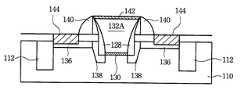
- third dielectric spacers 140are formed on the sidewalls of the first oxide spacers 122 by performing a conventional deposition process, followed by an etch-back process.
- a metal contact of the gate electrode 142 and the metal contacts of the source/drain electrodes 144are formed by a series of conventional processes of deposition, photolithography, and etching procedures.
- the metal contactsare compose of, but not limited to: W, Al/Cu alloy, Cu, and the like.
- the metal contactscan be deposited by a variety of techniques, such as high-density inductively coupled plasma (ICP) deposition, high-density ionized metal plasma (IMP) deposition, CVD, sputtering and the like.
- the key feature of the present inventionis that the width of the channel of the MOSFET, which is located beneath the gate dielectric layer 130 , is less than that of the first opening 118 , whose achievable minimum width equals to the photolithography limit. For this reason, the channel length of the recessed-gate according to the present invention is beyond the photolithography capability.
- the shrinkage amount of the channel lengthdepends on the width of the first oxide spacers 122 and thus on the thickness of the second dielectric layer 116 .
- the shrinkage amount of the channel length beyond the photolithography limitranges between 200 to 500 Angstroms (0.02 um to 0.05 um). [please confirm it]
Landscapes
- Engineering & Computer Science (AREA)
- Physics & Mathematics (AREA)
- Condensed Matter Physics & Semiconductors (AREA)
- General Physics & Mathematics (AREA)
- Manufacturing & Machinery (AREA)
- Computer Hardware Design (AREA)
- Microelectronics & Electronic Packaging (AREA)
- Power Engineering (AREA)
- Insulated Gate Type Field-Effect Transistor (AREA)
Abstract
Description
(1) Field of the Invention
The present invention relates generally to a method of manufacturing a MOSFET with a recessed-gate, and more particularly, to a method of forming a MOSFET with a recessed-gate having a channel length beyond the photolithography limit.
(2) Description of the Related Art
Integrated circuits (ICs), such as ultra-large scale integrated (ULSI) circuits, can include as many as one billion transistors or more. The ULSI circuits are generally composed of complementary metal oxide semiconductor field effect transistors (MOSFETs). Each MOSFET contains a gate electrode disposed between a drain region and a source region. In order to increase the device density and operating speed of the integrated circuits, the feature size of transistors within the circuits must be shrunk down. Particularly, in scaling down devices, a P-channel or an N-channel with shorter channel length is needed to enhance the operating speed.
Generally, photolithography process is a critical technique for shortening the channel length of a MOSFET. It is believed that the achievable minimum channel length depends on the photolithography limit of the lithographic tool, e.g. a stepper or a scanner.
In order to succeed at sub-0.1 μm gate dimensions and below, a recessed-gate MOSFET with out-diffused source/drain extension was disclosed in U.S. Pat. No. 6,093,947. Referring first to FIG. 1A, according to this prior art, a semiconductor wafer10 with a plurality of shallow trench isolation (STI)12 is provided. Apad oxide layer 34 and adielectric layer 36 are formed on thesemiconductor wafer 10. Next, ahole 38 is formed in the structure extending into thesemiconductor wafer 10. Thehole 38 has sidewalls and a bottom wall. Thereafter,oxide spacer regions 22 are formed on the sidewall of thehole 38, wherein theoxide spacer regions 22 contain a dopant material which can out-diffuse when subjected to annealing.
Referring now to FIG. 1B, agate oxide region 24 is formed on the bottom wall of thehole 38. After that, a conformal layer ofpolysilicon 40 is formed in thehole 38 and on thedielectric layer 36, and then a CMP process is performed to remove thepolysilicon layer 40 outside thehole 38, as shown in FIG.1B.
Referring now to FIG. 1C, thedielectric layer 36 is removed to expose thepad oxide layer 34 and outer walls of theoxide spacer regions 22. Source/drain regions 14/16 are formed in thesemiconductor wafer 10 adjacent to thehole 38.
Finally, as shown in FIG. 1D, an annealing process is performed to cause out-diffusion of the dopant from theoxide spacer regions 22 to thesemiconductor wafer 10 so as to form anextension 30 which wraps around theoxide spacer regions 22 and provides a connection to a channel region which is located beneath the gate oxide region. After that, nitridedouble spacers 19 are formed over thepad oxide layer 34. Finally, metal contacts, i.e.regions 32 and26, are formed in the structure.
However, according to the prior art, the achievalble minimum channel length equals to the photolithography limit, when the photolithography process for forming thehole 38 is performed under the photolithography limit. In order to obtain shorter channel length for improving operating speed, it will be necessary to develop a new technology for forming a MOSEET.
Accordingly, it is a primary object of the present invention to provide a method of forming a MOSFET with a recessed-gate having a channel length beyond the photolithography limit.
It is another object of the present invention to provide a method of forming a MOSFET with a recessed-gate.
A method of forming a MOSFET having a recessed-gate with a channel length beyond the photolithography limit is disclosed in the present invention. First, a first dielectric layer and a second dielectric layer are formed on a semiconductor substrate, wherein the first dielectric layer and the second dielectric layer have selective etchability. For example, the first dielectric layer is composed of silicon dioxide and the second dielectric layer is composed of silicon nitride or silicon oxynitride. The second dielectric layer has a thickness between 1000 to 2000 Angstroms.
Next, a first opening is formed in the second dielectric layer. After forming first spacers on sidewalls of the first opening and removing the first dielectric layer within the first opening, a trench is formed in the semiconductor substrate by an anisotropic etching process. After forming second spacers with dopant source material on sidewalls of the trench, a gate dielectric layer is formed within the trench.
Thereafter, a conductive layer is formed to refill said trench. After removing the portion of the conductive layer outside the trench, a gate plug is then formed. After removing the second dielectric layer, source and drain regions are formed by an ion implantation process. After that, source/drain extensions are formed by an annealing process to out-diffuse the dopant material to the semiconductor substrate.
Finally, after forming third spacers on sidewalls of the first spacers, metal contacts for the source and drain regions and the gate plug are formed.
The accompanying drawings forming a material part of this description, in which
FIG. 1A to FIG. 1D schematically illustrates the cross-sectional diagram of the method of forming a MOSFET with a recessed-gate according to the prior art.
FIG. 2A to FIG. 2J schematically illustrate the cross-sectional diagram of the method of forming a MOSFET with a recessed-gate having a channel length beyond the photolithography limit according to the present invention.
The present invention relates generally to a method of manufacturing a MOSFET with a recessed-gate, and more particularly, to a method of forming a MOSFET with a recessed-gate having a channel length beyond the photolithography limit.
Referring first to FIG. 2A, asemiconductor substrate 110 comprised of P-type single crystalline silicon is provided. Shallow trench isolation regions (STI)112 are next formed in thesemiconductor substrate 110. After that, a firstdielectric layer 114 and a seconddielectric layer 116 are formed on thesemiconductor substrate 110 in sequence.
The shallowtrench isolation regions 112 are formed by first forming shallow trenches in thesemiconductor substrate 110 using the conventional photolithographic and anisotropic reactive ion etching (RIE) procedures. After removal of the photoresist shape used to define the shallow trenches, a silicon oxide layer is deposited by low pressure chemical vapor deposition (LPCVD) or plasma enhanced chemical vapor deposition (PECVD) procedures for completely filling the shallow trenches. A chemical mechanical polishing (CMP) process is then performed to remove silicon oxide from the top surface of thesemiconductor substrate 110. Thefirst dielectric layer 114 is formed by conventional deposition process such as PECVD or LPCVD to a thickness between 50 to 200 Angstroms. Thefirst dielectric layer 114 is composed of silicon dioxide (SiO2), TiO2, Ta2O5and the like. Thesecond dielectric layer 116 is composed of silicon nitride or silicon oxynitride, and deposited by a low-pressure CVD (LPCVD) process or a plasma-enhanced CVD (PECVD) process to a thickness between 1000 to 2000 Angstroms. The first dielectric layer and the second dielectric layer should have selective etchability.
As shown in FIG. 2B, afirst opening 118 is formed in thesecond dielectric layer 116 by the conventional lithography and anisotropic etching techniques. The etching process is stopped on the top surface of thefirst dielectric layer 114. In one embodiment of the present invention, the lithography process is performed under the photolithography limit.
Referring now to FIG. 2C, a thirddielectric layer 120, composed of silicon dioxide, is deposited on thesecond dielectric layer 116 and in thefirst opening 118.
Referring now to FIG. 2D,first oxide spacers 122 are formed on the sidewalls of thefirst opening 118 by performing an anisotropic RIE process using CHF3as an etchant. Thefirst dielectric layer 114 in thefirst opening 118 is also removed during the etching process, and asecond opening 124 is simultaneously formed. The width of thesecond opening 124 is smaller than that of thefirst opening 118, as shown in FIG.2D.
Referring now to FIG. 2E, an anisotropic RIE process using Cl2as the etchant is performed to thesemiconductor substrate 110 through thesecond opening 124, and atrench 126 is formed. Because the etchant Cl2is blocked by thefirst oxide spacers 122 and thesecond dielectric layer 116, the width of thetrench 126 is less than that of thefirst opening 118 and thus beyond the photolithography limit, in case thefirst opening 18 is formed under the photolithography limit.
Referring now to FIG. 2F,second oxide spacers 128 containing a dopant source material are formed on the sidewalls of thetrench 126. A wet etching process is next performed to remove the surface defect of the silicon substrate. Thereafter, agate dielectric layer 130 is next formed on thesemiconductor substrate 110 within thetrench 126.
During the processes for forming thesecond oxide spacers 128, an oxide layer with a dopant source material is first deposited by a conventional deposition process such as PECVD or LPCVD. Thereafter, an anisotropic RIE process is performed to form thesecond oxide spacers 128. Thesecond oxide spacers 128 contain a P-type (e.g. B) or N-type (e.g. As, P) dopant source material, so that the dopant material can be out-diffused from thesecond oxide spacers 128 into thesemiconductor substrate 110 by annealing. The wet etching process is performed by a mixed solution of NH4F and HF, which shall etch silicon substrate only. Thegate dielectric layer 130 is comprised of silicon dioxide or nitrogen-rich oxide with a thickness between 10 to 50 Angstroms by a thermal oxidation process or a chemical vapor deposition process.
As shown in FIG. 2G, an electric conductive layerl32 is deposited on thegate dielectric layer 130, thesecond oxide spacers 128, and thesecond dielectric layer 116 to a thickness between 1000 to 3000 Angstroms. The electricconductive layer 132 is a conformal layer of doped polysilicon and formed by a LPCVD or a PECVD process. The polysilicon can be doped in-situ during deposition via the addition of boron, arsine, or phosphine to a silane ambient. On the other hand, the electricconductive layer 132 can be first deposited intrinsically, and then doped via an ion implantation process.
As shown in FIG. 2H, anelectric layer plug 132A is formed within thetrench 126 by a planarization process such as CMP process to remove the portion of the electric conductive layer outside thetrench 126.
Referring now to FIG. 21, a selective etching process is performed to remove thesecond dielectric layer 116. After that, an ion implantation process is performed to introducedopant ions 134 to form source/drain regions 136.
The selective etching process is performed by a wet etching process such as a hot phosphoric etch. The dose of thedopant ions 132 in the source/drain regions 136 ranges from 2E15 to 9E15 ions/cm2of theappropriate dopant ions 134, e.g., arsenic (As) or phosphorous (P) for an illustrative N-channel MOSFET (NMOS transistor) or boron (B) for an illustrative P-channel MOSFET (PMOS transistor). The implant energy of thedopant ions 134 ranges from approximately 15 to 25 keV. The dopant ions can thus be implanted to a depth of between 1000 to 2000 Angstroms within thesemiconductor substrate 110.
Referring now to FIG. 2J, an annealing process is first performed to out-diffuse the dopant source material in thesecond oxide spacers 128 into thesemiconductor substrate 110 to form source/drain extensions 138. The annealing process is generally performed by a rapid thermal annealing process (RTA). The source/drain extensions 138 wraps around thesecond oxide spacers 128 and connect the source/drain regions 136 to the channel which is located beneath thegate dielectric layer 130.
After that, thirddielectric spacers 140 are formed on the sidewalls of thefirst oxide spacers 122 by performing a conventional deposition process, followed by an etch-back process.
Finally, a metal contact of thegate electrode 142 and the metal contacts of the source/drain electrodes 144 are formed by a series of conventional processes of deposition, photolithography, and etching procedures. The metal contacts are compose of, but not limited to: W, Al/Cu alloy, Cu, and the like. The metal contacts can be deposited by a variety of techniques, such as high-density inductively coupled plasma (ICP) deposition, high-density ionized metal plasma (IMP) deposition, CVD, sputtering and the like.
The key feature of the present invention is that the width of the channel of the MOSFET, which is located beneath thegate dielectric layer 130, is less than that of thefirst opening 118, whose achievable minimum width equals to the photolithography limit. For this reason, the channel length of the recessed-gate according to the present invention is beyond the photolithography capability. The shrinkage amount of the channel length depends on the width of thefirst oxide spacers 122 and thus on the thickness of thesecond dielectric layer 116. The shrinkage amount of the channel length beyond the photolithography limit ranges between 200 to 500 Angstroms (0.02 um to 0.05 um). [please confirm it]
It should be understood that the foregoing relates to only preferred embodiments of the present invention, and that it is intended to cover all changes and modifications of the embodiments of the invention herein used for the purposes of the disclosure, which do not constitute departures from the spirit and scope of the invention.
Claims (8)
1. A method of forming a MOSFET having a recessed-gate with a channel length beyond photolithography limit, the method comprising:
a. forming a first dielectric layer and a second dielectric layer on a semiconductor substrate, wherein said first dielectric layer and said second dielectric layer have selective etchability;
b. forming a first opening in said second dielectric layer;
c. forming first spacers on sidewalls of said first opening and removing said first dielectric layer within said first opening;
d. forming a trench in said semiconductor substrate by an anisotropic etching process;
e. forming second spacers with dopant source material on sidewalls of said trench;
f. forming a gate dielectric layer within said trench;
g. forming a conductive layer to refill said trench;
h. removing a portion of said conductive layer outside said trench to form a gate plug;
i. removing said second dielectric layer;
j. forming source and drain regions and source/drain extensions;
k. forming third spacers on sidewalls of said first spacers; and
l. forming metal contacts for said source/drain regions and said gate plug.
2. The method ofclaim 1 , wherein said first opening is formed by a photolithography and an anisotropic etching processes, wherein said etching process is stopped on a top surface of said first dielectric layer.
3. The method ofclaim 1 , wherein said gate dielectric layer is formed by thermal oxidation process.
4. The method ofclaim 3 , wherein said gate dielectric layer has a thickness between 10 to 50 Angstroms.
5. The method ofclaim 1 , wherein said portion of said conductive layer outside said trench is removed by performing a chemical mechanical polishing process.
6. The method ofclaim 1 , wherein said source and drain regions are formed by an ion implantation process.
7. The method ofclaim 1 , wherein said source/drain extensions are formed by performing an annealing process to out-diffuse said dopant source material contained in said second spacers.
8. The method ofclaim 1 , wherein said first spacer, said second spacers and said third spacers are formed by first depositing an insulator layer and then performing an anisotropic etching process.
Priority Applications (1)
| Application Number | Priority Date | Filing Date | Title |
|---|---|---|---|
| US09/664,477US6358800B1 (en) | 2000-09-18 | 2000-09-18 | Method of forming a MOSFET with a recessed-gate having a channel length beyond photolithography limit |
Applications Claiming Priority (1)
| Application Number | Priority Date | Filing Date | Title |
|---|---|---|---|
| US09/664,477US6358800B1 (en) | 2000-09-18 | 2000-09-18 | Method of forming a MOSFET with a recessed-gate having a channel length beyond photolithography limit |
Publications (1)
| Publication Number | Publication Date |
|---|---|
| US6358800B1true US6358800B1 (en) | 2002-03-19 |
Family
ID=24666127
Family Applications (1)
| Application Number | Title | Priority Date | Filing Date |
|---|---|---|---|
| US09/664,477Expired - LifetimeUS6358800B1 (en) | 2000-09-18 | 2000-09-18 | Method of forming a MOSFET with a recessed-gate having a channel length beyond photolithography limit |
Country Status (1)
| Country | Link |
|---|---|
| US (1) | US6358800B1 (en) |
Cited By (65)
| Publication number | Priority date | Publication date | Assignee | Title |
|---|---|---|---|---|
| US20020094622A1 (en)* | 2000-09-27 | 2002-07-18 | Chartered Semiconductor Manufacturing Ltd. | Process flow for a performance enhanced MOSFET with self-aligned, recessed channel |
| US20020102793A1 (en)* | 2001-01-29 | 2002-08-01 | Ching-Yuan Wu | Method of fabricating a scalable stacked-gate flash memory device and its high-density memory arrays |
| US6534367B2 (en)* | 2001-04-28 | 2003-03-18 | Koninklijke Philips Electronics N.V. | Trench-gate semiconductor devices and their manufacture |
| US20040094797A1 (en)* | 2002-11-18 | 2004-05-20 | Il-Yong Park | MOS transistor having short channel and manufacturing method thereof |
| US20040126965A1 (en)* | 2002-12-27 | 2004-07-01 | Christian Krueger | Advanced recessed gate transistor and a method of forming the same |
| US20040132256A1 (en)* | 2002-12-13 | 2004-07-08 | Jae-Hun Kim | MOS transistor having a recessed gate electrode and fabrication method thereof |
| US20040168767A1 (en)* | 2003-02-27 | 2004-09-02 | Seiichiro Kanno | Semiconductor processing apparatus |
| US20040175907A1 (en)* | 2003-03-07 | 2004-09-09 | Taiwan Semiconductor Manfacturing Company | Method of fabricating a salicided device using a dummy dielectric layer between the source/drain and the gate electrode |
| US20050020086A1 (en)* | 2003-07-23 | 2005-01-27 | Ji-Young Kim | Self-aligned inner gate recess channel transistor and method of forming the same |
| US20050040475A1 (en)* | 2003-08-22 | 2005-02-24 | Young-Chul Jang | Transistors having a recessed channel region and methods of fabricating the same |
| US20050090084A1 (en)* | 2003-10-24 | 2005-04-28 | Woo Been J. | Method of forming a gate structure |
| US20050127433A1 (en)* | 2003-12-04 | 2005-06-16 | Taiwan Semiconductor Manufacturing Co., Ltd. | Recessed gate structure with reduced current leakage and overlap capacitance |
| US20050266692A1 (en)* | 2004-06-01 | 2005-12-01 | Brask Justin K | Method of patterning a film |
| KR100586547B1 (en)* | 2004-05-17 | 2006-06-08 | 주식회사 하이닉스반도체 | Semiconductor device having recessed gate and manufacturing method thereof |
| US20060138477A1 (en)* | 2004-12-24 | 2006-06-29 | Hynix Semiconductor, Inc. | Asymmetric recessed gate MOSFET and method for manufacturing the same |
| US20060186484A1 (en)* | 2005-02-23 | 2006-08-24 | Chau Robert S | Field effect transistor with narrow bandgap source and drain regions and method of fabrication |
| US20060220085A1 (en)* | 2005-03-31 | 2006-10-05 | Zong-Liang Huo | Single transistor floating body DRAM cell having recess channel transistor structure and method of fabricating the same |
| US20060261411A1 (en)* | 2003-06-27 | 2006-11-23 | Hareland Scott A | Nonplanar device with stress incorporation layer and method of fabrication |
| US20060286755A1 (en)* | 2005-06-15 | 2006-12-21 | Brask Justin K | Method for fabricating transistor with thinned channel |
| US20060289907A1 (en)* | 2003-01-16 | 2006-12-28 | Kim Sung-Min | Metal oxide semiconductor (MOS) transistors having buffer regions below source and drain regions and methods of fabricating the same |
| US20070007571A1 (en)* | 2005-07-06 | 2007-01-11 | Richard Lindsay | Semiconductor device with a buried gate and method of forming the same |
| US20070090408A1 (en)* | 2005-09-29 | 2007-04-26 | Amlan Majumdar | Narrow-body multiple-gate FET with dominant body transistor for high performance |
| US20070096185A1 (en)* | 2003-07-23 | 2007-05-03 | Samsung Electronics Co., Ltd | Method of forming self-aligned inner gate recess channel transistor |
| US20070111419A1 (en)* | 2005-09-28 | 2007-05-17 | Doyle Brian S | CMOS Devices with a single work function gate electrode and method of fabrication |
| US20070152266A1 (en)* | 2005-12-29 | 2007-07-05 | Intel Corporation | Method and structure for reducing the external resistance of a three-dimensional transistor through use of epitaxial layers |
| US20070184614A1 (en)* | 2004-12-15 | 2007-08-09 | International Business Machines Corporation | Recessed gate for a cmos image sensor |
| US20070221991A1 (en)* | 2006-03-23 | 2007-09-27 | Hynix Semiconductor Inc. | Semiconductor device with increased channel area and decreased leakage current |
| US20070262389A1 (en)* | 2004-01-16 | 2007-11-15 | Robert Chau | Tri-gate transistors and methods to fabricate same |
| US20080081432A1 (en)* | 2003-06-03 | 2008-04-03 | Kim Yong-Jin | Semiconductor device with trench gate type transistor and method of manufacturing the same |
| US20080142841A1 (en)* | 2004-03-31 | 2008-06-19 | Nick Lindert | Bulk non-planar transistor having strained enhanced mobility and methods of fabrication |
| US20080157225A1 (en)* | 2006-12-29 | 2008-07-03 | Suman Datta | SRAM and logic transistors with variable height multi-gate transistor architecture |
| US20080188041A1 (en)* | 2005-08-17 | 2008-08-07 | Suman Datta | Lateral undercut of metal gate in SOI device |
| US20080258207A1 (en)* | 2005-06-30 | 2008-10-23 | Marko Radosavljevic | Block Contact Architectures for Nanoscale Channel Transistors |
| US20090117699A1 (en)* | 2007-11-02 | 2009-05-07 | Promos Technologies Inc. | Method for preparing a recessed transistor structure |
| US20090149531A1 (en)* | 2007-12-11 | 2009-06-11 | Apoteknos Para La Piel, S.L. | Chemical composition derived from p-hydroxyphenyl propionic acid for the treatment of psoriasis |
| US20090206399A1 (en)* | 2003-10-10 | 2009-08-20 | Samsung Electronics Co., Ltd. | Method of forming a recess channel trench pattern, and fabricating a recess channel transistor |
| US20090215238A1 (en)* | 2002-12-18 | 2009-08-27 | Samsung Electronics Co., Ltd. | Methods of fabricating semiconductor devices with enlarged recessed gate electrodes |
| US20090218603A1 (en)* | 2005-06-21 | 2009-09-03 | Brask Justin K | Semiconductor device structures and methods of forming semiconductor structures |
| US20090273015A1 (en)* | 2008-04-30 | 2009-11-05 | Atmel Corporation | Non-volatile memory cell |
| US20090325350A1 (en)* | 2005-03-14 | 2009-12-31 | Marko Radosavljevic | Field effect transistor with metal source/drain regions |
| US20100013004A1 (en)* | 2008-07-16 | 2010-01-21 | Promos Technologies Inc. | Recessed channel transistor and method for preparing the same |
| US20100117147A1 (en)* | 2008-11-07 | 2010-05-13 | Sung-Hwan Kim | Capacitor-Less DRAM Device |
| US7820513B2 (en) | 2003-06-27 | 2010-10-26 | Intel Corporation | Nonplanar semiconductor device with partially or fully wrapped around gate electrode and methods of fabrication |
| US20100297838A1 (en)* | 2004-09-29 | 2010-11-25 | Chang Peter L D | Independently accessed double-gate and tri-gate transistors in same process flow |
| US20110062512A1 (en)* | 2004-10-25 | 2011-03-17 | Uday Shah | Nonplanar device with thinned lower body portion and method of fabrication |
| US7960794B2 (en) | 2004-08-10 | 2011-06-14 | Intel Corporation | Non-planar pMOS structure with a strained channel region and an integrated strained CMOS flow |
| US20110156145A1 (en)* | 2004-09-29 | 2011-06-30 | Marko Radosavljevic | Fabrication of channel wraparound gate structure for field-effect transistor |
| US7989280B2 (en) | 2005-11-30 | 2011-08-02 | Intel Corporation | Dielectric interface for group III-V semiconductor device |
| US8084818B2 (en) | 2004-06-30 | 2011-12-27 | Intel Corporation | High mobility tri-gate devices and methods of fabrication |
| US20120043585A1 (en)* | 2010-08-23 | 2012-02-23 | International Business Machines Corporation | Field Effect Transistor Device with Shaped Conduction Channel |
| US8193567B2 (en) | 2005-09-28 | 2012-06-05 | Intel Corporation | Process for integrating planar and non-planar CMOS transistors on a bulk substrate and article made thereby |
| US20120299185A1 (en)* | 2011-05-27 | 2012-11-29 | Tieh-Chiang Wu | Slit Recess Channel Gate and Method of Forming the Same |
| US8362566B2 (en) | 2008-06-23 | 2013-01-29 | Intel Corporation | Stress in trigate devices using complimentary gate fill materials |
| CN103151372A (en)* | 2011-12-07 | 2013-06-12 | 南亚科技股份有限公司 | Semiconductor structure with reinforced capping layer and method of making the same |
| US8617945B2 (en) | 2006-08-02 | 2013-12-31 | Intel Corporation | Stacking fault and twin blocking barrier for integrating III-V on Si |
| US20150115375A1 (en)* | 2013-10-24 | 2015-04-30 | Samsung Electronics Co., Ltd. | Semiconductor devices and methods of manufacturing the same |
| US20150236117A1 (en)* | 2014-02-14 | 2015-08-20 | Semi Solutions Llc | Reduced Variation MOSFET Using a Drain-Extension-Last Process |
| US20150295066A1 (en)* | 2012-09-05 | 2015-10-15 | Commissariat A L'energie Atomique Et Aux Ene Alt | Process for producing fet transistors |
| US9166045B1 (en)* | 2012-06-18 | 2015-10-20 | Altera Coporation | High-k dielectric device and process |
| CN110729191A (en)* | 2018-07-16 | 2020-01-24 | 台湾积体电路制造股份有限公司 | Reducing pattern loading in metal gate etch back |
| CN112086511A (en)* | 2019-06-13 | 2020-12-15 | 半导体元件工业有限责任公司 | System and method for self-aligned trench MOSFET contacts |
| US20230083560A1 (en)* | 2021-09-14 | 2023-03-16 | Sandisk Technologies Llc | Field effect transistors with gate fins and method of making the same |
| US11967626B2 (en) | 2021-09-14 | 2024-04-23 | Sandisk Technologies Llc | Field effect transistors with gate fins and method of making the same |
| CN118553619A (en)* | 2024-07-24 | 2024-08-27 | 杭州积海半导体有限公司 | MOSFET device formation method |
| US12279445B2 (en) | 2021-09-14 | 2025-04-15 | SanDisk Technologies, Inc. | Field effect transistors with gate fins and method of making the same |
Citations (12)
| Publication number | Priority date | Publication date | Assignee | Title |
|---|---|---|---|---|
| US5434093A (en)* | 1994-08-10 | 1995-07-18 | Intel Corporation | Inverted spacer transistor |
| US5448094A (en)* | 1994-08-23 | 1995-09-05 | United Microelectronics Corp. | Concave channel MOS transistor and method of fabricating the same |
| US5668021A (en)* | 1996-06-04 | 1997-09-16 | Motorola, Inc. | Process for fabricating a semiconductor device having a segmented channel region |
| US5780340A (en)* | 1996-10-30 | 1998-07-14 | Advanced Micro Devices, Inc. | Method of forming trench transistor and isolation trench |
| US6033980A (en)* | 1995-12-19 | 2000-03-07 | Stmicroelectronics, Inc. | Method of forming submicron contacts and vias in an integrated circuit |
| US6087208A (en)* | 1998-03-31 | 2000-07-11 | Advanced Micro Devices, Inc. | Method for increasing gate capacitance by using both high and low dielectric gate material |
| US6100146A (en)* | 1996-10-30 | 2000-08-08 | Advanced Micro Devices, Inc. | Method of forming trench transistor with insulative spacers |
| US6117712A (en)* | 1998-03-13 | 2000-09-12 | Texas Instruments - Acer Incorporated | Method of forming ultra-short channel and elevated S/D MOSFETS with a metal gate on SOI substrate |
| US6130454A (en)* | 1998-07-07 | 2000-10-10 | Advanced Micro Devices, Inc. | Gate conductor formed within a trench bounded by slanted sidewalls |
| US6171916B1 (en)* | 1997-09-22 | 2001-01-09 | Nippon Steel Corporation | Semiconductor device having buried gate electrode with silicide layer and manufacture method thereof |
| US6204128B1 (en)* | 1998-10-26 | 2001-03-20 | Matsushita Electronics Corporation | Method for fabricating semiconductor device |
| US6204133B1 (en)* | 2000-06-02 | 2001-03-20 | Advanced Micro Devices, Inc. | Self-aligned extension junction for reduced gate channel |
- 2000
- 2000-09-18USUS09/664,477patent/US6358800B1/ennot_activeExpired - Lifetime
Patent Citations (12)
| Publication number | Priority date | Publication date | Assignee | Title |
|---|---|---|---|---|
| US5434093A (en)* | 1994-08-10 | 1995-07-18 | Intel Corporation | Inverted spacer transistor |
| US5448094A (en)* | 1994-08-23 | 1995-09-05 | United Microelectronics Corp. | Concave channel MOS transistor and method of fabricating the same |
| US6033980A (en)* | 1995-12-19 | 2000-03-07 | Stmicroelectronics, Inc. | Method of forming submicron contacts and vias in an integrated circuit |
| US5668021A (en)* | 1996-06-04 | 1997-09-16 | Motorola, Inc. | Process for fabricating a semiconductor device having a segmented channel region |
| US5780340A (en)* | 1996-10-30 | 1998-07-14 | Advanced Micro Devices, Inc. | Method of forming trench transistor and isolation trench |
| US6100146A (en)* | 1996-10-30 | 2000-08-08 | Advanced Micro Devices, Inc. | Method of forming trench transistor with insulative spacers |
| US6171916B1 (en)* | 1997-09-22 | 2001-01-09 | Nippon Steel Corporation | Semiconductor device having buried gate electrode with silicide layer and manufacture method thereof |
| US6117712A (en)* | 1998-03-13 | 2000-09-12 | Texas Instruments - Acer Incorporated | Method of forming ultra-short channel and elevated S/D MOSFETS with a metal gate on SOI substrate |
| US6087208A (en)* | 1998-03-31 | 2000-07-11 | Advanced Micro Devices, Inc. | Method for increasing gate capacitance by using both high and low dielectric gate material |
| US6130454A (en)* | 1998-07-07 | 2000-10-10 | Advanced Micro Devices, Inc. | Gate conductor formed within a trench bounded by slanted sidewalls |
| US6204128B1 (en)* | 1998-10-26 | 2001-03-20 | Matsushita Electronics Corporation | Method for fabricating semiconductor device |
| US6204133B1 (en)* | 2000-06-02 | 2001-03-20 | Advanced Micro Devices, Inc. | Self-aligned extension junction for reduced gate channel |
Cited By (147)
| Publication number | Priority date | Publication date | Assignee | Title |
|---|---|---|---|---|
| US20020094622A1 (en)* | 2000-09-27 | 2002-07-18 | Chartered Semiconductor Manufacturing Ltd. | Process flow for a performance enhanced MOSFET with self-aligned, recessed channel |
| US7091092B2 (en)* | 2000-09-27 | 2006-08-15 | Chartered Semiconductor Manufacturing Ltd. | Process flow for a performance enhanced MOSFET with self-aligned, recessed channel |
| US20020102793A1 (en)* | 2001-01-29 | 2002-08-01 | Ching-Yuan Wu | Method of fabricating a scalable stacked-gate flash memory device and its high-density memory arrays |
| US6534367B2 (en)* | 2001-04-28 | 2003-03-18 | Koninklijke Philips Electronics N.V. | Trench-gate semiconductor devices and their manufacture |
| US20040214382A1 (en)* | 2002-11-18 | 2004-10-28 | Il-Yong Park | Method of manufacturing MOS transistor having short channel |
| US20040094797A1 (en)* | 2002-11-18 | 2004-05-20 | Il-Yong Park | MOS transistor having short channel and manufacturing method thereof |
| US20040132256A1 (en)* | 2002-12-13 | 2004-07-08 | Jae-Hun Kim | MOS transistor having a recessed gate electrode and fabrication method thereof |
| US7550352B2 (en) | 2002-12-13 | 2009-06-23 | Samsung Electronics Co., Ltd. | MOS transistor having a recessed gate electrode and fabrication method thereof |
| US20050233513A1 (en)* | 2002-12-13 | 2005-10-20 | Samsung Electronics Co., Ltd. | MOS transistor having a recessed gate electrode and fabrication method thereof |
| US6924529B2 (en) | 2002-12-13 | 2005-08-02 | Samsung Electronics Co., Ltd. | MOS transistor having a recessed gate electrode and fabrication method thereof |
| US7871914B2 (en)* | 2002-12-18 | 2011-01-18 | Samsung Electronics Co., Ltd. | Methods of fabricating semiconductor devices with enlarged recessed gate electrodes |
| US20090215238A1 (en)* | 2002-12-18 | 2009-08-27 | Samsung Electronics Co., Ltd. | Methods of fabricating semiconductor devices with enlarged recessed gate electrodes |
| US6897114B2 (en)* | 2002-12-27 | 2005-05-24 | Advanced Micro Devices, Inc. | Methods of forming a transistor having a recessed gate electrode structure |
| US20040126965A1 (en)* | 2002-12-27 | 2004-07-01 | Christian Krueger | Advanced recessed gate transistor and a method of forming the same |
| US7541645B2 (en)* | 2003-01-16 | 2009-06-02 | Samsung Electronics Co., Ltd. | Metal oxide semiconductor (MOS) transistors having buffer regions below source and drain regions |
| US20060289907A1 (en)* | 2003-01-16 | 2006-12-28 | Kim Sung-Min | Metal oxide semiconductor (MOS) transistors having buffer regions below source and drain regions and methods of fabricating the same |
| US20040168767A1 (en)* | 2003-02-27 | 2004-09-02 | Seiichiro Kanno | Semiconductor processing apparatus |
| US20040175907A1 (en)* | 2003-03-07 | 2004-09-09 | Taiwan Semiconductor Manfacturing Company | Method of fabricating a salicided device using a dummy dielectric layer between the source/drain and the gate electrode |
| US20080081432A1 (en)* | 2003-06-03 | 2008-04-03 | Kim Yong-Jin | Semiconductor device with trench gate type transistor and method of manufacturing the same |
| US7709346B2 (en)* | 2003-06-03 | 2010-05-04 | Samsung Electronics Co., Ltd. | Semiconductor device with trench gate type transistor and method of manufacturing the same |
| US8273626B2 (en) | 2003-06-27 | 2012-09-25 | Intel Corporationn | Nonplanar semiconductor device with partially or fully wrapped around gate electrode and methods of fabrication |
| US8405164B2 (en) | 2003-06-27 | 2013-03-26 | Intel Corporation | Tri-gate transistor device with stress incorporation layer and method of fabrication |
| US7714397B2 (en) | 2003-06-27 | 2010-05-11 | Intel Corporation | Tri-gate transistor device with stress incorporation layer and method of fabrication |
| US20060261411A1 (en)* | 2003-06-27 | 2006-11-23 | Hareland Scott A | Nonplanar device with stress incorporation layer and method of fabrication |
| US20100200917A1 (en)* | 2003-06-27 | 2010-08-12 | Hareland Scott A | Nonplanar device with stress incorporation layer and method of fabrication |
| US7820513B2 (en) | 2003-06-27 | 2010-10-26 | Intel Corporation | Nonplanar semiconductor device with partially or fully wrapped around gate electrode and methods of fabrication |
| US20050020086A1 (en)* | 2003-07-23 | 2005-01-27 | Ji-Young Kim | Self-aligned inner gate recess channel transistor and method of forming the same |
| US20070096185A1 (en)* | 2003-07-23 | 2007-05-03 | Samsung Electronics Co., Ltd | Method of forming self-aligned inner gate recess channel transistor |
| US7154144B2 (en) | 2003-07-23 | 2006-12-26 | Samsung Electronics Co., Ltd. | Self-aligned inner gate recess channel transistor and method of forming the same |
| US7670910B2 (en) | 2003-07-23 | 2010-03-02 | Samsung Electronics Co., Ltd. | Method of forming self-aligned inner gate recess channel transistor |
| US20060270138A1 (en)* | 2003-08-22 | 2006-11-30 | Young-Chul Jang | Transistors having a recessed channel region and methods of fabricating the same |
| US20050040475A1 (en)* | 2003-08-22 | 2005-02-24 | Young-Chul Jang | Transistors having a recessed channel region and methods of fabricating the same |
| US7141851B2 (en)* | 2003-08-22 | 2006-11-28 | Samsung Electronics Co., Ltd. | Transistors having a recessed channel region |
| US20090206399A1 (en)* | 2003-10-10 | 2009-08-20 | Samsung Electronics Co., Ltd. | Method of forming a recess channel trench pattern, and fabricating a recess channel transistor |
| US20050090084A1 (en)* | 2003-10-24 | 2005-04-28 | Woo Been J. | Method of forming a gate structure |
| US7012014B2 (en)* | 2003-12-04 | 2006-03-14 | Taiwan Semiconductor Manufacturing Co., Ltd | Recessed gate structure with reduced current leakage and overlap capacitance |
| US20050127433A1 (en)* | 2003-12-04 | 2005-06-16 | Taiwan Semiconductor Manufacturing Co., Ltd. | Recessed gate structure with reduced current leakage and overlap capacitance |
| US20070262389A1 (en)* | 2004-01-16 | 2007-11-15 | Robert Chau | Tri-gate transistors and methods to fabricate same |
| US7781771B2 (en) | 2004-03-31 | 2010-08-24 | Intel Corporation | Bulk non-planar transistor having strained enhanced mobility and methods of fabrication |
| US20080142841A1 (en)* | 2004-03-31 | 2008-06-19 | Nick Lindert | Bulk non-planar transistor having strained enhanced mobility and methods of fabrication |
| KR100586547B1 (en)* | 2004-05-17 | 2006-06-08 | 주식회사 하이닉스반도체 | Semiconductor device having recessed gate and manufacturing method thereof |
| US20050266692A1 (en)* | 2004-06-01 | 2005-12-01 | Brask Justin K | Method of patterning a film |
| US7579280B2 (en) | 2004-06-01 | 2009-08-25 | Intel Corporation | Method of patterning a film |
| US8084818B2 (en) | 2004-06-30 | 2011-12-27 | Intel Corporation | High mobility tri-gate devices and methods of fabrication |
| US7960794B2 (en) | 2004-08-10 | 2011-06-14 | Intel Corporation | Non-planar pMOS structure with a strained channel region and an integrated strained CMOS flow |
| US8399922B2 (en) | 2004-09-29 | 2013-03-19 | Intel Corporation | Independently accessed double-gate and tri-gate transistors |
| US20100297838A1 (en)* | 2004-09-29 | 2010-11-25 | Chang Peter L D | Independently accessed double-gate and tri-gate transistors in same process flow |
| US20110156145A1 (en)* | 2004-09-29 | 2011-06-30 | Marko Radosavljevic | Fabrication of channel wraparound gate structure for field-effect transistor |
| US8268709B2 (en) | 2004-09-29 | 2012-09-18 | Intel Corporation | Independently accessed double-gate and tri-gate transistors in same process flow |
| US8749026B2 (en) | 2004-10-25 | 2014-06-10 | Intel Corporation | Nonplanar device with thinned lower body portion and method of fabrication |
| US8502351B2 (en) | 2004-10-25 | 2013-08-06 | Intel Corporation | Nonplanar device with thinned lower body portion and method of fabrication |
| US10236356B2 (en) | 2004-10-25 | 2019-03-19 | Intel Corporation | Nonplanar device with thinned lower body portion and method of fabrication |
| US20110062512A1 (en)* | 2004-10-25 | 2011-03-17 | Uday Shah | Nonplanar device with thinned lower body portion and method of fabrication |
| US9741809B2 (en) | 2004-10-25 | 2017-08-22 | Intel Corporation | Nonplanar device with thinned lower body portion and method of fabrication |
| US9190518B2 (en) | 2004-10-25 | 2015-11-17 | Intel Corporation | Nonplanar device with thinned lower body portion and method of fabrication |
| US8067818B2 (en) | 2004-10-25 | 2011-11-29 | Intel Corporation | Nonplanar device with thinned lower body portion and method of fabrication |
| US7572701B2 (en)* | 2004-12-15 | 2009-08-11 | International Business Machines Corporation | Recessed gate for a CMOS image sensor |
| US20070184614A1 (en)* | 2004-12-15 | 2007-08-09 | International Business Machines Corporation | Recessed gate for a cmos image sensor |
| US20060138477A1 (en)* | 2004-12-24 | 2006-06-29 | Hynix Semiconductor, Inc. | Asymmetric recessed gate MOSFET and method for manufacturing the same |
| US7723768B2 (en) | 2004-12-24 | 2010-05-25 | Hynix Semiconductor Inc. | Asymmetric recessed gate MOSFET and method for manufacturing the same |
| US20060186484A1 (en)* | 2005-02-23 | 2006-08-24 | Chau Robert S | Field effect transistor with narrow bandgap source and drain regions and method of fabrication |
| US20110121393A1 (en)* | 2005-02-23 | 2011-05-26 | Chau Robert S | Field effect transistor with narrow bandgap source and drain regions and method of fabrication |
| US9048314B2 (en) | 2005-02-23 | 2015-06-02 | Intel Corporation | Field effect transistor with narrow bandgap source and drain regions and method of fabrication |
| US8183646B2 (en) | 2005-02-23 | 2012-05-22 | Intel Corporation | Field effect transistor with narrow bandgap source and drain regions and method of fabrication |
| US8368135B2 (en) | 2005-02-23 | 2013-02-05 | Intel Corporation | Field effect transistor with narrow bandgap source and drain regions and method of fabrication |
| US8664694B2 (en) | 2005-02-23 | 2014-03-04 | Intel Corporation | Field effect transistor with narrow bandgap source and drain regions and method of fabrication |
| US9368583B2 (en) | 2005-02-23 | 2016-06-14 | Intel Corporation | Field effect transistor with narrow bandgap source and drain regions and method of fabrication |
| US8816394B2 (en) | 2005-02-23 | 2014-08-26 | Intel Corporation | Field effect transistor with narrow bandgap source and drain regions and method of fabrication |
| US7893506B2 (en) | 2005-02-23 | 2011-02-22 | Intel Corporation | Field effect transistor with narrow bandgap source and drain regions and method of fabrication |
| US7825481B2 (en) | 2005-02-23 | 2010-11-02 | Intel Corporation | Field effect transistor with narrow bandgap source and drain regions and method of fabrication |
| US20090142897A1 (en)* | 2005-02-23 | 2009-06-04 | Chau Robert S | Field effect transistor with narrow bandgap source and drain regions and method of fabrication |
| US20100295129A1 (en)* | 2005-02-23 | 2010-11-25 | Chau Robert S | Field effect transistor with narrow bandgap source and drain regions and method of fabrication |
| US7518196B2 (en) | 2005-02-23 | 2009-04-14 | Intel Corporation | Field effect transistor with narrow bandgap source and drain regions and method of fabrication |
| US20090325350A1 (en)* | 2005-03-14 | 2009-12-31 | Marko Radosavljevic | Field effect transistor with metal source/drain regions |
| US7879675B2 (en) | 2005-03-14 | 2011-02-01 | Intel Corporation | Field effect transistor with metal source/drain regions |
| US7338862B2 (en)* | 2005-03-31 | 2008-03-04 | Samsung Electronics Co., Ltd. | Methods of fabricating a single transistor floating body DRAM cell having recess channel transistor structure |
| US20060220085A1 (en)* | 2005-03-31 | 2006-10-05 | Zong-Liang Huo | Single transistor floating body DRAM cell having recess channel transistor structure and method of fabricating the same |
| US20060286755A1 (en)* | 2005-06-15 | 2006-12-21 | Brask Justin K | Method for fabricating transistor with thinned channel |
| US9806195B2 (en) | 2005-06-15 | 2017-10-31 | Intel Corporation | Method for fabricating transistor with thinned channel |
| US20110062520A1 (en)* | 2005-06-15 | 2011-03-17 | Brask Justin K | Method for fabricating transistor with thinned channel |
| US11978799B2 (en) | 2005-06-15 | 2024-05-07 | Tahoe Research, Ltd. | Method for fabricating transistor with thinned channel |
| US10937907B2 (en) | 2005-06-15 | 2021-03-02 | Intel Corporation | Method for fabricating transistor with thinned channel |
| US7858481B2 (en)* | 2005-06-15 | 2010-12-28 | Intel Corporation | Method for fabricating transistor with thinned channel |
| US10367093B2 (en) | 2005-06-15 | 2019-07-30 | Intel Corporation | Method for fabricating transistor with thinned channel |
| US9337307B2 (en)* | 2005-06-15 | 2016-05-10 | Intel Corporation | Method for fabricating transistor with thinned channel |
| US8933458B2 (en) | 2005-06-21 | 2015-01-13 | Intel Corporation | Semiconductor device structures and methods of forming semiconductor structures |
| US20090218603A1 (en)* | 2005-06-21 | 2009-09-03 | Brask Justin K | Semiconductor device structures and methods of forming semiconductor structures |
| US8071983B2 (en) | 2005-06-21 | 2011-12-06 | Intel Corporation | Semiconductor device structures and methods of forming semiconductor structures |
| US9761724B2 (en) | 2005-06-21 | 2017-09-12 | Intel Corporation | Semiconductor device structures and methods of forming semiconductor structures |
| US8581258B2 (en) | 2005-06-21 | 2013-11-12 | Intel Corporation | Semiconductor device structures and methods of forming semiconductor structures |
| US9385180B2 (en) | 2005-06-21 | 2016-07-05 | Intel Corporation | Semiconductor device structures and methods of forming semiconductor structures |
| US20080258207A1 (en)* | 2005-06-30 | 2008-10-23 | Marko Radosavljevic | Block Contact Architectures for Nanoscale Channel Transistors |
| US7898041B2 (en) | 2005-06-30 | 2011-03-01 | Intel Corporation | Block contact architectures for nanoscale channel transistors |
| US8338887B2 (en) | 2005-07-06 | 2012-12-25 | Infineon Technologies Ag | Buried gate transistor |
| US20070007571A1 (en)* | 2005-07-06 | 2007-01-11 | Richard Lindsay | Semiconductor device with a buried gate and method of forming the same |
| US9059141B2 (en) | 2005-07-06 | 2015-06-16 | Infineon Technologies Ag | Buried gate transistor |
| US8796762B2 (en) | 2005-07-06 | 2014-08-05 | Infineon Technologies Ag | Buried gate transistor |
| US20080188041A1 (en)* | 2005-08-17 | 2008-08-07 | Suman Datta | Lateral undercut of metal gate in SOI device |
| US7736956B2 (en) | 2005-08-17 | 2010-06-15 | Intel Corporation | Lateral undercut of metal gate in SOI device |
| US8193567B2 (en) | 2005-09-28 | 2012-06-05 | Intel Corporation | Process for integrating planar and non-planar CMOS transistors on a bulk substrate and article made thereby |
| US20070111419A1 (en)* | 2005-09-28 | 2007-05-17 | Doyle Brian S | CMOS Devices with a single work function gate electrode and method of fabrication |
| US20110180851A1 (en)* | 2005-09-28 | 2011-07-28 | Doyle Brian S | Cmos devices with a single work function gate electrode and method of fabrication |
| US7902014B2 (en) | 2005-09-28 | 2011-03-08 | Intel Corporation | CMOS devices with a single work function gate electrode and method of fabrication |
| US8294180B2 (en) | 2005-09-28 | 2012-10-23 | Intel Corporation | CMOS devices with a single work function gate electrode and method of fabrication |
| US20070090408A1 (en)* | 2005-09-29 | 2007-04-26 | Amlan Majumdar | Narrow-body multiple-gate FET with dominant body transistor for high performance |
| US7989280B2 (en) | 2005-11-30 | 2011-08-02 | Intel Corporation | Dielectric interface for group III-V semiconductor device |
| US20070152266A1 (en)* | 2005-12-29 | 2007-07-05 | Intel Corporation | Method and structure for reducing the external resistance of a three-dimensional transistor through use of epitaxial layers |
| US20070221991A1 (en)* | 2006-03-23 | 2007-09-27 | Hynix Semiconductor Inc. | Semiconductor device with increased channel area and decreased leakage current |
| US7910989B2 (en) | 2006-03-23 | 2011-03-22 | Hynix Semiconductor Inc. | Semiconductor device with increased channel area and decreased leakage current |
| US20100072541A1 (en)* | 2006-03-23 | 2010-03-25 | Hynix Semiconductor Inc. | Semiconductor device with increased channel area and decreased leakage current |
| US7592210B2 (en) | 2006-03-23 | 2009-09-22 | Hynix Semiconductor Inc. | Semiconductor device with increased channel area and decreased leakage current |
| US8617945B2 (en) | 2006-08-02 | 2013-12-31 | Intel Corporation | Stacking fault and twin blocking barrier for integrating III-V on Si |
| US20080157225A1 (en)* | 2006-12-29 | 2008-07-03 | Suman Datta | SRAM and logic transistors with variable height multi-gate transistor architecture |
| US20090117699A1 (en)* | 2007-11-02 | 2009-05-07 | Promos Technologies Inc. | Method for preparing a recessed transistor structure |
| US20090149531A1 (en)* | 2007-12-11 | 2009-06-11 | Apoteknos Para La Piel, S.L. | Chemical composition derived from p-hydroxyphenyl propionic acid for the treatment of psoriasis |
| US20090273015A1 (en)* | 2008-04-30 | 2009-11-05 | Atmel Corporation | Non-volatile memory cell |
| US9450092B2 (en) | 2008-06-23 | 2016-09-20 | Intel Corporation | Stress in trigate devices using complimentary gate fill materials |
| US8741733B2 (en) | 2008-06-23 | 2014-06-03 | Intel Corporation | Stress in trigate devices using complimentary gate fill materials |
| US9806193B2 (en) | 2008-06-23 | 2017-10-31 | Intel Corporation | Stress in trigate devices using complimentary gate fill materials |
| US8362566B2 (en) | 2008-06-23 | 2013-01-29 | Intel Corporation | Stress in trigate devices using complimentary gate fill materials |
| US9224754B2 (en) | 2008-06-23 | 2015-12-29 | Intel Corporation | Stress in trigate devices using complimentary gate fill materials |
| US7781830B2 (en)* | 2008-07-16 | 2010-08-24 | Promos Technologies Inc. | Recessed channel transistor and method for preparing the same |
| US20100013004A1 (en)* | 2008-07-16 | 2010-01-21 | Promos Technologies Inc. | Recessed channel transistor and method for preparing the same |
| US20100117147A1 (en)* | 2008-11-07 | 2010-05-13 | Sung-Hwan Kim | Capacitor-Less DRAM Device |
| US9041057B2 (en) | 2010-08-23 | 2015-05-26 | International Business Machines Corporation | Field effect transistor device with shaped conduction channel |
| US8309418B2 (en)* | 2010-08-23 | 2012-11-13 | International Business Machines Corporation | Field effect transistor device with shaped conduction channel |
| US20120043585A1 (en)* | 2010-08-23 | 2012-02-23 | International Business Machines Corporation | Field Effect Transistor Device with Shaped Conduction Channel |
| US20120299185A1 (en)* | 2011-05-27 | 2012-11-29 | Tieh-Chiang Wu | Slit Recess Channel Gate and Method of Forming the Same |
| US8530306B2 (en)* | 2011-05-27 | 2013-09-10 | Nanya Technology Corp. | Method of forming a slit recess channel gate |
| US8698235B2 (en) | 2011-05-27 | 2014-04-15 | Nanya Technology Corp. | Slit recess channel gate |
| CN103151372A (en)* | 2011-12-07 | 2013-06-12 | 南亚科技股份有限公司 | Semiconductor structure with reinforced capping layer and method of making the same |
| US9166045B1 (en)* | 2012-06-18 | 2015-10-20 | Altera Coporation | High-k dielectric device and process |
| US11264479B2 (en)* | 2012-09-05 | 2022-03-01 | Commissariat A L'energie Atomique Et Aux Energies Alternatives | Process for producing FET transistors |
| US20150295066A1 (en)* | 2012-09-05 | 2015-10-15 | Commissariat A L'energie Atomique Et Aux Ene Alt | Process for producing fet transistors |
| US20150115375A1 (en)* | 2013-10-24 | 2015-04-30 | Samsung Electronics Co., Ltd. | Semiconductor devices and methods of manufacturing the same |
| US9508820B2 (en)* | 2013-10-24 | 2016-11-29 | Samsung Electronics Company, Ltd. | Semiconductor devices and methods of manufacturing the same |
| US9379214B2 (en)* | 2014-02-14 | 2016-06-28 | Semi Solutions Llc | Reduced variation MOSFET using a drain-extension-last process |
| US20150236117A1 (en)* | 2014-02-14 | 2015-08-20 | Semi Solutions Llc | Reduced Variation MOSFET Using a Drain-Extension-Last Process |
| CN110729191B (en)* | 2018-07-16 | 2023-08-29 | 台湾积体电路制造股份有限公司 | Reducing pattern loading in back etching of metal gates |
| CN110729191A (en)* | 2018-07-16 | 2020-01-24 | 台湾积体电路制造股份有限公司 | Reducing pattern loading in metal gate etch back |
| CN112086511A (en)* | 2019-06-13 | 2020-12-15 | 半导体元件工业有限责任公司 | System and method for self-aligned trench MOSFET contacts |
| US12243778B2 (en) | 2019-06-13 | 2025-03-04 | Semiconductor Components Industries, Llc | Self-aligned semiconductor device contacts having widths less than minimum lithography limits |
| US20230083560A1 (en)* | 2021-09-14 | 2023-03-16 | Sandisk Technologies Llc | Field effect transistors with gate fins and method of making the same |
| US11967626B2 (en) | 2021-09-14 | 2024-04-23 | Sandisk Technologies Llc | Field effect transistors with gate fins and method of making the same |
| US12015084B2 (en)* | 2021-09-14 | 2024-06-18 | Sandisk Technologies Llc | Field effect transistors with gate fins and method of making the same |
| US12279445B2 (en) | 2021-09-14 | 2025-04-15 | SanDisk Technologies, Inc. | Field effect transistors with gate fins and method of making the same |
| CN118553619A (en)* | 2024-07-24 | 2024-08-27 | 杭州积海半导体有限公司 | MOSFET device formation method |
Similar Documents
| Publication | Publication Date | Title |
|---|---|---|
| US6358800B1 (en) | Method of forming a MOSFET with a recessed-gate having a channel length beyond photolithography limit | |
| US6524901B1 (en) | Method for forming a notched damascene planar poly/metal gate | |
| US6737308B2 (en) | Semiconductor device having LDD-type source/drain regions and fabrication method thereof | |
| US6235574B1 (en) | High performance DRAM and method of manufacture | |
| US6337262B1 (en) | Self aligned T-top gate process integration | |
| US7994572B2 (en) | MOSFET having recessed channel | |
| US6908801B2 (en) | Method of manufacturing semiconductor device | |
| US5406111A (en) | Protection device for an intergrated circuit and method of formation | |
| US7361537B2 (en) | Method of fabricating recess channel array transistor | |
| US6165871A (en) | Method of making low-leakage architecture for sub-0.18 μm salicided CMOS device | |
| US6340614B1 (en) | Method of forming a DRAM cell | |
| US20060177983A1 (en) | Method for forming a notched gate | |
| US6475916B1 (en) | Method of patterning gate electrode with ultra-thin gate dielectric | |
| US6204137B1 (en) | Method to form transistors and local interconnects using a silicon nitride dummy gate technique | |
| US6432774B2 (en) | Method of fabricating memory cell with trench capacitor and vertical transistor | |
| US6403485B1 (en) | Method to form a low parasitic capacitance pseudo-SOI CMOS device | |
| US5612240A (en) | Method for making electrical connections to self-aligned contacts that extends beyond the photo-lithographic resolution limit | |
| US6180465B1 (en) | Method of making high performance MOSFET with channel scaling mask feature | |
| US6297530B1 (en) | Self aligned channel implantation | |
| US5834350A (en) | Elevated transistor fabrication technique | |
| US20040038461A1 (en) | Semiconductor device on silicon-on-insulator and method for manufacturing the semiconductor device | |
| US6046088A (en) | Method for self-aligning polysilicon gates with field isolation and the resultant structure | |
| JP7021821B2 (en) | Low cost flash memory manufacturing flow based on metal gate process | |
| US6784098B1 (en) | Method for forming salicide process | |
| US6306741B1 (en) | Method of patterning gate electrodes with high K gate dielectrics |
Legal Events
| Date | Code | Title | Description |
|---|---|---|---|
| AS | Assignment | Owner name:VANGUARD INTERNATIONAL SEMICONDUCTOR COPRORATION, Free format text:ASSIGNMENT OF ASSIGNORS INTEREST;ASSIGNOR:TSENG, HORNG-HUEI;REEL/FRAME:011133/0072 Effective date:20000905 | |
| STCF | Information on status: patent grant | Free format text:PATENTED CASE | |
| FPAY | Fee payment | Year of fee payment:4 | |
| FPAY | Fee payment | Year of fee payment:8 | |
| FPAY | Fee payment | Year of fee payment:12 |