US6357904B1 - Linear illumination device - Google Patents
Linear illumination deviceDownload PDFInfo
- Publication number
- US6357904B1 US6357904B1US09/548,150US54815000AUS6357904B1US 6357904 B1US6357904 B1US 6357904B1US 54815000 AUS54815000 AUS 54815000AUS 6357904 B1US6357904 B1US 6357904B1
- Authority
- US
- United States
- Prior art keywords
- light
- light source
- optical waveguide
- emitting
- waveguide member
- Prior art date
- Legal status (The legal status is an assumption and is not a legal conclusion. Google has not performed a legal analysis and makes no representation as to the accuracy of the status listed.)
- Expired - Fee Related
Links
Images


Classifications
- G—PHYSICS
- G02—OPTICS
- G02F—OPTICAL DEVICES OR ARRANGEMENTS FOR THE CONTROL OF LIGHT BY MODIFICATION OF THE OPTICAL PROPERTIES OF THE MEDIA OF THE ELEMENTS INVOLVED THEREIN; NON-LINEAR OPTICS; FREQUENCY-CHANGING OF LIGHT; OPTICAL LOGIC ELEMENTS; OPTICAL ANALOGUE/DIGITAL CONVERTERS
- G02F1/00—Devices or arrangements for the control of the intensity, colour, phase, polarisation or direction of light arriving from an independent light source, e.g. switching, gating or modulating; Non-linear optics
- G02F1/01—Devices or arrangements for the control of the intensity, colour, phase, polarisation or direction of light arriving from an independent light source, e.g. switching, gating or modulating; Non-linear optics for the control of the intensity, phase, polarisation or colour
- G02F1/13—Devices or arrangements for the control of the intensity, colour, phase, polarisation or direction of light arriving from an independent light source, e.g. switching, gating or modulating; Non-linear optics for the control of the intensity, phase, polarisation or colour based on liquid crystals, e.g. single liquid crystal display cells
- G02F1/133—Constructional arrangements; Operation of liquid crystal cells; Circuit arrangements
- G02F1/1333—Constructional arrangements; Manufacturing methods
- G02F1/1335—Structural association of cells with optical devices, e.g. polarisers or reflectors
- H—ELECTRICITY
- H01—ELECTRIC ELEMENTS
- H01L—SEMICONDUCTOR DEVICES NOT COVERED BY CLASS H10
- H01L25/00—Assemblies consisting of a plurality of semiconductor or other solid state devices
- H01L25/03—Assemblies consisting of a plurality of semiconductor or other solid state devices all the devices being of a type provided for in a single subclass of subclasses H10B, H10D, H10F, H10H, H10K or H10N, e.g. assemblies of rectifier diodes
- H01L25/04—Assemblies consisting of a plurality of semiconductor or other solid state devices all the devices being of a type provided for in a single subclass of subclasses H10B, H10D, H10F, H10H, H10K or H10N, e.g. assemblies of rectifier diodes the devices not having separate containers
- H01L25/075—Assemblies consisting of a plurality of semiconductor or other solid state devices all the devices being of a type provided for in a single subclass of subclasses H10B, H10D, H10F, H10H, H10K or H10N, e.g. assemblies of rectifier diodes the devices not having separate containers the devices being of a type provided for in group H10H20/00
- H01L25/0753—Assemblies consisting of a plurality of semiconductor or other solid state devices all the devices being of a type provided for in a single subclass of subclasses H10B, H10D, H10F, H10H, H10K or H10N, e.g. assemblies of rectifier diodes the devices not having separate containers the devices being of a type provided for in group H10H20/00 the devices being arranged next to each other
- G—PHYSICS
- G02—OPTICS
- G02B—OPTICAL ELEMENTS, SYSTEMS OR APPARATUS
- G02B6/00—Light guides; Structural details of arrangements comprising light guides and other optical elements, e.g. couplings
- G02B6/0001—Light guides; Structural details of arrangements comprising light guides and other optical elements, e.g. couplings specially adapted for lighting devices or systems
- G—PHYSICS
- G02—OPTICS
- G02B—OPTICAL ELEMENTS, SYSTEMS OR APPARATUS
- G02B6/00—Light guides; Structural details of arrangements comprising light guides and other optical elements, e.g. couplings
- G02B6/24—Coupling light guides
- G02B6/42—Coupling light guides with opto-electronic elements
- G02B6/4298—Coupling light guides with opto-electronic elements coupling with non-coherent light sources and/or radiation detectors, e.g. lamps, incandescent bulbs, scintillation chambers
- H—ELECTRICITY
- H01—ELECTRIC ELEMENTS
- H01L—SEMICONDUCTOR DEVICES NOT COVERED BY CLASS H10
- H01L2924/00—Indexing scheme for arrangements or methods for connecting or disconnecting semiconductor or solid-state bodies as covered by H01L24/00
- H01L2924/0001—Technical content checked by a classifier
- H01L2924/0002—Not covered by any one of groups H01L24/00, H01L24/00 and H01L2224/00
- H—ELECTRICITY
- H10—SEMICONDUCTOR DEVICES; ELECTRIC SOLID-STATE DEVICES NOT OTHERWISE PROVIDED FOR
- H10H—INORGANIC LIGHT-EMITTING SEMICONDUCTOR DEVICES HAVING POTENTIAL BARRIERS
- H10H20/00—Individual inorganic light-emitting semiconductor devices having potential barriers, e.g. light-emitting diodes [LED]
- H10H20/80—Constructional details
- H10H20/85—Packages
- H10H20/855—Optical field-shaping means, e.g. lenses
- Y—GENERAL TAGGING OF NEW TECHNOLOGICAL DEVELOPMENTS; GENERAL TAGGING OF CROSS-SECTIONAL TECHNOLOGIES SPANNING OVER SEVERAL SECTIONS OF THE IPC; TECHNICAL SUBJECTS COVERED BY FORMER USPC CROSS-REFERENCE ART COLLECTIONS [XRACs] AND DIGESTS
- Y10—TECHNICAL SUBJECTS COVERED BY FORMER USPC
- Y10S—TECHNICAL SUBJECTS COVERED BY FORMER USPC CROSS-REFERENCE ART COLLECTIONS [XRACs] AND DIGESTS
- Y10S362/00—Illumination
- Y10S362/80—Light emitting diode
Definitions
- the present inventionrelates to a linear illumination device and, particularly, to a linear illumination device suitable for use as a light source of a contact type color image sensor.
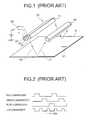
- Japanese Patent Application Laid-open No. H10-56577discloses a construction of a conventional long linear illumination device for a color image sensor, which is schematically shown in FIG. 1 .
- FIG. 1in order to obtain a color signal corresponding to an image of an original 9 , each identical portion of the original is illuminated with a red (R), green (G) and blue (B) lights from R, G and B color light emitting diodes (LED's) while switching these LED's by a switch circuit 60 with a light emitting timing shown in FIG. 2 .
- LED's 21 , 22 and 23 corresponding to R, G and B color lights, respectively,are arranged on an end surface of an optical waveguide member 11 and emit an illumination light 45 containing R, G and B color lights downward by guiding them through the optical waveguide member 11 while scattering them suitably.
- the original 9 disposed below the optical waveguide member 11is illuminated with the illumination light 45 and a reflection light 47 reflected from the surface of the original 9 is incident on an image sensor 50 , which is composed of a sensor array, through an optical system, etc., which is not shown.
- the image sensor 50converts each color light into an electric signal with a light-electric conversion timing as shown in the bottom of FIG. 2, so that an electric color information for every scan line of the original is obtained.
- the reliability of the blue color light emitting LEDis not sufficient at present and the supply thereof is not enough, the cost of the blue LED becomes very high. Consequently, the cost of the linear illumination device itself becomes high.
- An object of the present inventionis to provide an inexpensive linear illumination device capable of realizing an improvement of uniformity of a distribution of illumination light in a lengthwise direction of a linear light source thereof.
- a linear illumination devicecomprises an optical waveguide member for guiding three primary color lights incident on a light incident surface thereof and emitting them from a rectangular linear light emitting surface thereof, a point light source including at least one light emitting diode (referred to as LED, hereinafter), etc., provided on the optical waveguide member for supplying light through the light incident surface of the optical waveguide member into an interior thereof and a surface emitting light source including at least one light emitting element such as organic electro luminescent (referred to as EL, hereinafter) element provided on a surface portion of the optical waveguide member other than the light emitting surface thereof for reflecting back the light emitted from the point light source into the interior of the optical waveguide member.
- ELorganic electro luminescent
- a rear side electrode, that is a cathode electrode, of the EL element opposite to a transparent electrode, that is, an anode electrode, thereofis constituted with a light-reflecting layer of such as aluminum.
- An LEDis employed as a red color light source and an EL element is employed as a blue color light source.
- a green color light sourceeither LED or EL element is employed.
- a linear illumination deviceis obtained by providing the red color LED on an end face of the optical waveguide member and the two EL elements on an upper surface of the optical waveguide member.
- the linear illumination deviceby providing a plurality of red color LED's on the upper surface of the optical waveguide member and the two EL elements on respective opposite side surfaces of the optical waveguide member.
- the linear illumination deviceis obtained by providing a red color LED and a green color LED on the end face of the optical waveguide member and the blue color EL element on the upper surface of the optical waveguide member.
- the EL elementis preferably an organic thin film EL element including a transparent front electrode as an anode electrode on the side of the optical waveguide member, a metal rear electrode as a cathode electrode, which may be formed of aluminum and has a light reflecting function and an organic thin film light emitting layer provided between the transparent front electrode and the metal rear electrode.
- the linear illumination deviceis constructed such that the point light source and a surface emitting light source emit three primary color lights sequentially. Further, the metal rear electrode of the EL element is formed to cover the upper and side surfaces of the optical waveguide member to thereby effectively reflect light in an interior of the optical waveguide member and guide it to the light emitting surface thereof.
- the linear illumination devicecan use not only EL element but also LED for emitting blue color light. Therefore, it is possible to reduce the cost of linear illumination device when the LED is used as the blue color light source. Further, according to the present invention, LED or LED's and EL element or elements are combined suitably. Therefore, it is possible to employ an inexpensive construction of linear illumination device. Further, since the EL element is a surface light emitting element, it is possible to illuminate a plane to be illuminated with high uniformity.
- the design of the optical waveguide member for uniformly diffusing light to a linear lightbecomes substantially easier compared with the conventional design for uniformly diffusing lights having different wavelengths and the uniformity of illumination can be improved compared with the conventional case.
- both the blue and green color lightsmay be emitted by the EL elements. Therefore, no unevenness of amounts of blue and green color lights occurs due to the rectangular parallelepiped optical waveguide member and a uniform illumination for an original to be illuminated can be obtained. Consequently, the light amount of illumination is uniformed, so that it becomes possible to improve the quality of image taken in by converting a reflected light reflected by the original illuminated by the linear illumination device into an electric signal by an image sensor.
- FIG. 1is a schematic perspective view of a color image sensor employing a conventional linear illumination device having three primary color LED's as a point light source;
- FIG. 2shows light emitting timings of the three primary colors from the LED's shown in FIG. 1 and a light-electric conversion timing thereof at a light receiving portion thereof;
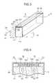
- FIG. 3is a schematic perspective view of an illumination device for a contact type sensor, according to a first embodiment of the present invention
- FIG. 4is an enlarged cross sectional view of the illumination device taken along a line A—A in FIG. 3;
- FIG. 5is a schematic perspective view of an illumination device for a contact type sensor, according to a second embodiment of the present invention.
- FIG. 6is a schematic perspective view of an illumination device for a contact type sensor, according to a third embodiment of the present invention.
- FIG. 7is a schematic perspective view of an illumination device for a contact type sensor, according to a fourth embodiment of the present invention.
- FIG. 8is a schematic cross sectional view of a contact type image sensor integrated with the linear illumination device shown in FIG. 3 .
- an optical waveguide member 11 having a rectangular parallelepiped shapeis formed of a transparent material such as transparent glass and has a lower light emitting surface 114 for emitting three primary color lights in a direction shown by an arrow 45 .
- a red color light emitting LED 21is provided on an end face 111 of the optical waveguide member 11 adjacent to the shorter side of the light emitting face 114 thereof.
- a rectangular green EL element 32 for emitting green color light and a rectangular blue EL element 33 emitting blue color lightare provided in parallel to each other on and along an upper surface of the optical waveguide member 11 , as rectangular surface emitting light sources.
- the LED 21may be embedded into the end face 111 of the optical waveguide member 11 .
- the green EL element 32is constructed with a transparent anode electrode 321 of such as tin-doped indium oxide (referred to as ITO, hereinafter) formed on the upper surface of the optical waveguide member 11 , a green light emitting layer 320 formed on the transparent electrode 321 and a metal rear electrode 3 of such as aluminum formed on the green light emitting layer 320 as a cathode.
- ITOtin-doped indium oxide
- the blue EL element 33is constructed with a transparent anode electrode 331 of such as ITO formed on the upper surface of the optical waveguide member 11 , a blue light emitting layer 330 formed on the transparent anode electrode 331 and the metal rear electrode 3 , which is formed on the blue light emitting layer 330 and functions as a light reflecting film as well.
- ConfigGurations of the transparent electrodes 321 and 331are identical in plane to the respective light emitting layers thereof.
- the metal rear electrode 3 functioning as the light reflecting film as wellare used commonly for the green and blue EL elements.
- the light reflecting electrode 3is larger in plane area than the light emitting layers as well as the transparent electrodes and extends to not only the upper surface of the optical waveguide member 11 but also the longer side surfaces of the light emitting surface 114 thereof such that lights incident to an interior of the optical waveguide member 11 is reflected thereby to efficiently emit the three primary color lights from the light emitting surface 114 .
- an application of voltage to the LED 21 and the EL elements 32 and 33is sequentially switched by a switch circuit 60 according to the light emitting timings shown in FIG. 2 to sequentially emit the three primary R, G and B lights so that the light source switching type color image sensor can be realized.
- Either inorganic EL elements or organic EL elementscan be used as the EL elements 32 and 33 .
- organic EL elementswhich can be driven with a low D.C. voltage, are preferable in view of simplicity of the drive circuit design.
- the present inventionis not limited to any specific construction of organic EL elements. In the following description, the present invention will be described as using organic EL elements.
- FIG. 4shows a case where known organic thin film EL elements each having a light emitting layer containing three-layer structure are employed in the linear illumination device having the construction shown in FIG. 3 .
- the organic EL element 32 emitting green color lightis formed by forming the transparent front electrode 321 on the upper surface of the optical waveguide member 11 , forming a hole transporting organic thin film 322 on the transparent electrode 321 , forming a green color light emitting organic thin layer 320 on the hole transporting organic thin film 322 , forming an electron transporting organic thin layer 323 on the green color light emitting organic thin layer 320 and forming the metal rear electrode 3 functioning as a reflection film, which is used commonly by the organic EL element 33 for emitting blue color light.
- the organic EL element 33 emitting blue color lightis formed by forming the transparent electrode 331 on the upper surface of the optical waveguide member 11 , forming a hole transporting organic thin film 322 on the transparent electrode 331 , forming a blue color light emitting organic thin layer 330 on the hole transporting organic thin film 332 , forming an electron transporting organic thin layer 333 on the blue color light emitting organic thin layer 330 and using the metal rear electrode 3 of the organic EL element 33 .
- the metal rear electrode 3which is common for the organic EL elements 32 and 33 , is electrically separated from the transparent electrodes 321 and 331 .
- a spaceis provided between the organic EL elements 32 and 33 and spaces are provided between the side faces of the organic EL elements and the metal rear electrode 3 , respectively.
- these spacesmay be filled with a suitable insulating material.
- the reflecting electrode 3 of aluminumis used as the cathode electrode applied with ground potential.
- a positive voltageis applied to the transparent anode electrodes 321 and 331 of the organic EL elements 32 and 33 and to the red LED 21 with the respective light emitting timings shown in FIG. 2, the organic thin film light emitting layers 320 and 330 and the red LED 21 emit green, blue and red lights sequentially, respectively.
- the red color light emitted from the LED 21is reflected by the metal rear electrode 3 of aluminum as a cathode provided on a rear surface of the organic EL elements. That is, the organic EL elements function as a reflection plate when the LED 21 emits red color light. Further, since the respective organic EL elements are surface emitting light sources, it becomes possible to illuminate the original with highly uniform luminance.
- the red color LED 21provided on the optical waveguide member 11 and the organic EL elements 32 and 33 provided on the upper surface of the optical waveguide member 11 in parallel each other and emitting green and blue color lights, respectively, and the organic EL elements are arranged such that the red color light from the LED 21 in the optical waveguide member 11 is reflected back thereby, it becomes possible to reduce the cost of the linear illumination device, to illuminate the original with lights from the organic EL elements highly uniformly and to substantially facilitate the design of the optical waveguide member compared with the conventional design, to thereby improve the quality of the taken-in image.
- FIG. 5shows a linear illumination device for a contact type color image sensor, according to a second embodiment of the present invention.
- the linear illumination device shown in FIG. 5employs two LED's as red and green color light emitters and an organic EL element as a blue color light emitter.
- the LED 21 capable of emitting red color light and an LED 22 capable of emitting green color light, which can be independently driven each other,are juxtaposed on one of end faces of an optical waveguide member 11 .
- An organic EL element 33 capable of emitting blue color lightis formed on substantially a whole upper surface of the optical waveguide member 11 .
- An output lightis emitted from a lower surface of the optical waveguide member 11 in a direction shown by an arrow 45 .
- the organic EL element 33 capable of emitting blue color lighthas a similar construction of the organic EL element 33 shown in FIG. 4 . That is, the organic EL element 33 of the second embodiment comprises a transparent electrode 331 , an organic thin film light emitting layer 330 and a metal rear electrode 3 as a cathode. Incidentally, a light source switching and driving device for these LED's and the organic EL element is not shown since it is similar to that shown in FIG. 3 .
- the light emitted from either one of the LED's, which is currently driven,is reflected by the metal rear electrode 3 of such as aluminum as the cathode provided on a rear surface of the organic EL element 33 as well. That is, the organic EL element 33 functions as a reflection plate when either one of the LED's emits light. Further, since the organic EL element 33 is a surface-emitting element, it becomes possible to illuminate the original with highly uniform luminance. It should be noted that green light among the three primary color lights can be obtained by an organic EL element instead of the LED.
- the second embodiment of the present inventionwhich comprises the LED 22 for emitting green color light arranged on the end face of the rectangular parallelepiped optical waveguide member 11 , it becomes possible to reduce the cost of the linear illumination device, to illuminate the original with lights from the organic EL element 33 highly uniformly and to substantially facilitate the design of the optical waveguide member compared with the conventional design, to thereby improve the quality of the taken-in image.
- the metal rear cathode electrode 23 of aluminum of the organic EL element 33functions as the reflection plate, providing the same effect as that obtained in the first embodiment.
- FIG. 6shows a linear illumination device for the contact type color image sensor according to a third embodiment of the present invention.
- the linear illumination devicecomprises an organic EL element 33 for emitting blue color light provided on an upper surface of the rectangular parallelepiped optical waveguide member 11 .
- the organic EL element 33has a similar construction to that shown in FIG. 5 .
- a plurality of openings 306are formed in a rear side portion of a cathode electrode 3 , through which the optical waveguide member 11 is partially exposed.
- a plurality of red color light emitting LED's 21 and a plurality of green light emitting LED's 22are provided in the openings 306 , alternately.
- six (6) openings 306are provided equidistantly in a lengthwise direction of the optical waveguide member 11 and three red LED's and three green LED's are arranged in the openings 306 alternately.
- a light source switching and driving device for these LED's and the EL elementis not shown since it is similar to that shown in FIG. 3 .
- the illumination device shown in FIG. 6illuminates an original by guiding the primary R, G and B color lights emitted from LED's 21 and 22 , which emit red and green color light, respectively, and an organic EL element 33 , which emits blue color light, through an optical waveguide member 11 to a lower surface thereof and emitting the R, G and B color lights therefrom in a direction shown by an arrow 45 .
- LED's 21 and 22which emit red and green color light, respectively
- an organic EL element 33which emits blue color light
- FIG. 7A linear illumination device for a contact type color image sensor according to a fourth embodiment of the present invention will be described with reference to FIG. 7 .
- an organic EL element 32 capable of emitting green color light and an organic EL element 33 capable of emitting blue color lightare arranged on opposite side surfaces of an optical waveguide member 11 having a rectangular parallelepiped shape, respectively.
- a plurality of LED's 21 capable of emitting red color lightare arranged equidistantly on an upper surface of the optical waveguide member 11 .
- openings 307are formed equidistantly in a portion of a cathode electrode 3 common for the organic EL elements 32 and 33 , which abuts the upper surface of the optical waveguide member 11 , along a lengthwise direction of the optical waveguide member 11 and the LED's 21 are fixed in the openings 307 , respectively.
- the three primary color lights emitted from the organic EL elements 32 and 33 and the LED's 21are guided by the optical waveguide member 11 and emitted from a bottom surface thereof in a direction shown by an arrow 45 .
- the organic EL elements 32 and 33have similar construction to those of the EL elements mentioned previously.
- the organic EL element 32 for emitting green color lightis formed by forming a rectangular transparent anode electrode 321 on one of the side surfaces of the optical waveguide member 11 and forming an organic thin film light emitting layer 320 thereon.
- the organic EL element 33 for emitting blue color lightis formed by forming a transparent anode electrode 331 on the other side surface of the optical waveguide member 11 and forming an organic thin film light emitting layer 330 thereon.
- the three primary color lights emitted from the LED's 21 and the paired organic EL elements 32 and 33are guided by the optical waveguide member 11 and emitted from the lower surface of the optical waveguide member 11 in the direction shown by the arrow 45 to uniformly illuminate the original.
- the LED's 21which emit red color light
- the organic EL elements 32 and 33which emit blue and green color lights, respectively, and are arranged oppositely such that these organic EL elements function as reflection films internally reflecting light substantially totally, the improvement of light emitting efficiency and the reduction of cost can be realized.
- red lights from the LED's 21are also totally internally reflected by the organic EL elements 32 and 33 and guided in the direction shown by the arrow 45 .
- a light source switching and driving device for these LED's and the EL elementsis not shown since it is similar to that shown in FIG. 3 .
- the organic EL elements 32 and 33are arranged on the opposite side surfaces of the rectangular parallelepiped optical waveguide member 11 in order to obtain a required amount of light, it becomes possible to reduce the cost of the linear illumination device, to illuminate the original with lights from the organic EL element 33 highly uniformly and to substantially facilitate the design of the optical waveguide member compared with the conventional design, to thereby improve the quality of the taken-in image as in the case of the first embodiment. Further, since the aluminum cathode electrode 3 common for the organic EL elements 32 and 33 has the function of a reflection plate when these EL elements are not driven, the same effect as that obtained by the first embodiment can be obtained.
- the linear illumination devicecan be used to an information reading in an image scanner or an image reading in a facsimile device.
- the linear illumination devicemay be combined with a line image sensor to make it possible to read an original with high resolution under high illumination condition.
- FIG. 8shows a construction of an integrated contact type image sensor, in which the linear illumination device shown in FIG. 1 is integrated with a contact type image sensor.
- the output light emitted from the lower surface of the optical waveguide member 11illuminates an original 9 below an optical member 80 through a transparent substrate 70 having a thin film transistor (referred to as TFT, hereinafter) image sensor 71 and an optical waveguide member 81 , such as glass fiber, of the optical member 80 .
- Reflection light from the original 9is received by the TFT image sensor 71 through the optical waveguide member 81 to read an image of the original.
- TFTthin film transistor
- the constructive relation between the linear illumination device of the present invention and the line image sensoris not limited to the integrated construction shown in FIG. 8 .
- the construction shown FIG. 1may be employed.
- the linear illumination devicein which an organic EL element is used to obtain blue color light, it is unnecessary to use the very expensive blue LED, so that it becomes possible to reduce the cost of the linear illumination device. Further, since the organic EL element emitting blue color light is relatively easily available, it is possible to obtain an inexpensive construction by combining an LED or LED's and an organic EL element or elements, as a light source.
- the organic EL elementis a surface emitting light source, it is possible to illuminate an object with highly uniform light from the organic EL element or elements.
- the red color LEDis a point light source, it is possible to define the light emitting area to a point. Therefore, the design of the optical waveguide member for uniformly diffusing light to a linear light becomes substantially easier compared with the conventional design for uniformly diffusing lights having different wavelengths and the uniformity of illumination can be improved compared with the conventional case.
- both the blue and green color lightsmay be emitted by the surface emitting light sources. Therefore, no unevenness of amount of light occurs due to the long linear optical waveguide member and a uniform illumination for an original as to be illuminated can be obtained. Consequently, the light amount of illumination is uniformed and it is possible to improve the quality of image taken in by converting a reflected light reflected by the original illuminated by the linear illumination device by means of an image sensor.
Landscapes
- Physics & Mathematics (AREA)
- Engineering & Computer Science (AREA)
- Microelectronics & Electronic Packaging (AREA)
- Power Engineering (AREA)
- General Physics & Mathematics (AREA)
- Computer Hardware Design (AREA)
- Condensed Matter Physics & Semiconductors (AREA)
- Nonlinear Science (AREA)
- Mathematical Physics (AREA)
- Chemical & Material Sciences (AREA)
- Crystallography & Structural Chemistry (AREA)
- Optics & Photonics (AREA)
- Electroluminescent Light Sources (AREA)
- Facsimile Scanning Arrangements (AREA)
- Facsimile Heads (AREA)
Abstract
Description
Claims (17)
Applications Claiming Priority (2)
| Application Number | Priority Date | Filing Date | Title |
|---|---|---|---|
| JP11098099 | 1999-04-19 | ||
| JP11-110980 | 1999-04-19 |
Publications (1)
| Publication Number | Publication Date |
|---|---|
| US6357904B1true US6357904B1 (en) | 2002-03-19 |
Family
ID=14549361
Family Applications (1)
| Application Number | Title | Priority Date | Filing Date |
|---|---|---|---|
| US09/548,150Expired - Fee RelatedUS6357904B1 (en) | 1999-04-19 | 2000-04-13 | Linear illumination device |
Country Status (3)
| Country | Link |
|---|---|
| US (1) | US6357904B1 (en) |
| KR (1) | KR100379243B1 (en) |
| TW (1) | TW498676B (en) |
Cited By (31)
| Publication number | Priority date | Publication date | Assignee | Title |
|---|---|---|---|---|
| US6601962B1 (en)* | 1999-05-11 | 2003-08-05 | Nichia Corporation | Surface light emitting device |
| US20030210556A1 (en)* | 2002-05-09 | 2003-11-13 | Wu Rong Yaw | Linear light source device for image reading |
| US20030210557A1 (en)* | 2002-05-09 | 2003-11-13 | Rong-Yaw Wu | Linear light source device for image reading |
| US20040075748A1 (en)* | 2002-10-16 | 2004-04-22 | Exar Corporation | Pixel-by-pixel digital control of gain and offset correction for video imaging |
| US20040109664A1 (en)* | 2002-07-26 | 2004-06-10 | Advanced Display Inc. | Planar light source device and liquid crystal display device using the same |
| US20040213008A1 (en)* | 2002-12-23 | 2004-10-28 | Lisa Draxlmaier Gmbh | Lighting system for displays in vehicles |
| US20040252479A1 (en)* | 2003-06-13 | 2004-12-16 | Che-Kuei Mai | [back light module and liquid crystal display] |
| US20040264190A1 (en)* | 2003-06-24 | 2004-12-30 | Creative Sensor Inc. | Light source module structure for CIS module |
| US6851832B2 (en) | 2002-05-21 | 2005-02-08 | Dwayne A. Tieszen | Led tube light housings |
| US20050152146A1 (en)* | 2002-05-08 | 2005-07-14 | Owen Mark D. | High efficiency solid-state light source and methods of use and manufacture |
| US20050195614A1 (en)* | 2002-12-23 | 2005-09-08 | Lisa Draxlmaier Gmbh | Lighting system for displays in vehicles |
| US20060063288A1 (en)* | 2003-05-13 | 2006-03-23 | Heng Liu | High power AllnGaN based multi-chip light emitting diode |
| US20060146540A1 (en)* | 2004-12-30 | 2006-07-06 | Ann Reo | Linear lighting apparatus with increased light-transmission efficiency |
| US20060146531A1 (en)* | 2004-12-30 | 2006-07-06 | Ann Reo | Linear lighting apparatus with improved heat dissipation |
| US20060255349A1 (en)* | 2004-05-11 | 2006-11-16 | Heng Liu | High power AllnGaN based multi-chip light emitting diode |
| US20070076427A1 (en)* | 2004-12-30 | 2007-04-05 | Ann Reo | Linear lighting apparatus with increased light- transmission efficiency |
| US20070171661A1 (en)* | 2005-12-16 | 2007-07-26 | Jean-Louis Desvaud | Striplight and system with high-power light-emitting diodes for an automatic fault detection system |
| US20070278504A1 (en)* | 2002-05-08 | 2007-12-06 | Roland Jasmin | Methods and systems relating to solid state light sources for use in industrial processes |
| USD565750S1 (en)* | 2005-11-16 | 2008-04-01 | Toshiba Lighting & Technology Corporation | Light emitting diode lamp |
| US20090141002A1 (en)* | 2007-12-03 | 2009-06-04 | Lg Display Co., Ltd. | Touch panel display device |
| US20090262545A1 (en)* | 2008-04-21 | 2009-10-22 | Joerg Amelung | Illumination Apparatus and Method of Producing a Planar Light Output |
| US7638808B2 (en) | 2004-03-18 | 2009-12-29 | Phoseon Technology, Inc. | Micro-reflectors on a substrate for high-density LED array |
| US20100128483A1 (en)* | 2008-11-25 | 2010-05-27 | Cooper Technologies Company | Led luminaire |
| US20100219040A1 (en)* | 2006-02-23 | 2010-09-02 | Masanori Nakamori | Escalator display device |
| US20110110085A1 (en)* | 2009-11-12 | 2011-05-12 | Cooper Technologies Company | Light Emitting Diode Module |
| US20120169945A1 (en)* | 2009-09-16 | 2012-07-05 | Sharp Kabushiki Kaisha | Lighting device, display device, and television receiver |
| US8616720B2 (en) | 2010-04-27 | 2013-12-31 | Cooper Technologies Company | Linkable linear light emitting diode system |
| US8764220B2 (en) | 2010-04-28 | 2014-07-01 | Cooper Technologies Company | Linear LED light module |
| US9576694B2 (en) | 2010-09-17 | 2017-02-21 | Drexel University | Applications for alliform carbon |
| US9752932B2 (en) | 2010-03-10 | 2017-09-05 | Drexel University | Tunable electro-optic filter stack |
| US10197254B2 (en) | 2017-02-09 | 2019-02-05 | Walthill Opportunities, L.L.C. | Strut light system with integrated light source |
Families Citing this family (1)
| Publication number | Priority date | Publication date | Assignee | Title |
|---|---|---|---|---|
| KR20030067225A (en)* | 2002-02-07 | 2003-08-14 | 주식회사 반디부리 | The plane lighting display system using LED and light diffusion sheet |
Citations (5)
| Publication number | Priority date | Publication date | Assignee | Title |
|---|---|---|---|---|
| US5396406A (en)* | 1993-02-01 | 1995-03-07 | Display Technology Industries | Thin high efficiency illumination system for display devices |
| US5709453A (en)* | 1994-08-16 | 1998-01-20 | Krent; Edward D. | Vehicle lighting having remote light source |
| JPH1056577A (en) | 1996-06-06 | 1998-02-24 | Canon Inc | Image reading device, image reading system, light source control device, and storage medium |
| US5810463A (en)* | 1994-11-28 | 1998-09-22 | Nikon Corporation | Illumination device |
| US6139174A (en)* | 1998-08-25 | 2000-10-31 | Hewlett-Packard Company | Light source assembly for scanning devices utilizing light emitting diodes |
Family Cites Families (1)
| Publication number | Priority date | Publication date | Assignee | Title |
|---|---|---|---|---|
| KR0161468B1 (en)* | 1995-11-29 | 1999-03-20 | 김광호 | Close Image Sensor |
- 2000
- 2000-04-13USUS09/548,150patent/US6357904B1/ennot_activeExpired - Fee Related
- 2000-04-15TWTW089107063Apatent/TW498676B/ennot_activeIP Right Cessation
- 2000-04-19KRKR10-2000-0020834Apatent/KR100379243B1/ennot_activeExpired - Fee Related
Patent Citations (5)
| Publication number | Priority date | Publication date | Assignee | Title |
|---|---|---|---|---|
| US5396406A (en)* | 1993-02-01 | 1995-03-07 | Display Technology Industries | Thin high efficiency illumination system for display devices |
| US5709453A (en)* | 1994-08-16 | 1998-01-20 | Krent; Edward D. | Vehicle lighting having remote light source |
| US5810463A (en)* | 1994-11-28 | 1998-09-22 | Nikon Corporation | Illumination device |
| JPH1056577A (en) | 1996-06-06 | 1998-02-24 | Canon Inc | Image reading device, image reading system, light source control device, and storage medium |
| US6139174A (en)* | 1998-08-25 | 2000-10-31 | Hewlett-Packard Company | Light source assembly for scanning devices utilizing light emitting diodes |
Cited By (63)
| Publication number | Priority date | Publication date | Assignee | Title |
|---|---|---|---|---|
| US7063450B2 (en) | 1999-05-11 | 2006-06-20 | Nichia Corporation | Surface light emitting device |
| US20030214818A1 (en)* | 1999-05-11 | 2003-11-20 | Nichia Corporation | Surface light emitting device |
| US6601962B1 (en)* | 1999-05-11 | 2003-08-05 | Nichia Corporation | Surface light emitting device |
| US8496356B2 (en) | 2002-05-08 | 2013-07-30 | Phoseon Technology, Inc. | High efficiency solid-state light source and methods of use and manufacture |
| US7461949B2 (en) | 2002-05-08 | 2008-12-09 | Phoseon Technology, Inc. | Methods and systems relating to solid state light sources for use in industrial processes |
| US8192053B2 (en) | 2002-05-08 | 2012-06-05 | Phoseon Technology, Inc. | High efficiency solid-state light source and methods of use and manufacture |
| US20050152146A1 (en)* | 2002-05-08 | 2005-07-14 | Owen Mark D. | High efficiency solid-state light source and methods of use and manufacture |
| US20070278504A1 (en)* | 2002-05-08 | 2007-12-06 | Roland Jasmin | Methods and systems relating to solid state light sources for use in industrial processes |
| US10401012B2 (en) | 2002-05-08 | 2019-09-03 | Phoseon Technology, Inc. | High efficiency solid-state light source and methods of use and manufacture |
| US6851816B2 (en)* | 2002-05-09 | 2005-02-08 | Pixon Technologies Corp. | Linear light source device for image reading |
| US6786626B2 (en)* | 2002-05-09 | 2004-09-07 | Pixon Technologies Corp. | Linear light source device for image reading |
| US20030210557A1 (en)* | 2002-05-09 | 2003-11-13 | Rong-Yaw Wu | Linear light source device for image reading |
| US20030210556A1 (en)* | 2002-05-09 | 2003-11-13 | Wu Rong Yaw | Linear light source device for image reading |
| US6851832B2 (en) | 2002-05-21 | 2005-02-08 | Dwayne A. Tieszen | Led tube light housings |
| US6976779B2 (en)* | 2002-07-26 | 2005-12-20 | Advanced Display Inc. | Planar light source device and liquid crystal display device using the same |
| US20040109664A1 (en)* | 2002-07-26 | 2004-06-10 | Advanced Display Inc. | Planar light source device and liquid crystal display device using the same |
| US20040075748A1 (en)* | 2002-10-16 | 2004-04-22 | Exar Corporation | Pixel-by-pixel digital control of gain and offset correction for video imaging |
| US7038720B2 (en)* | 2002-10-16 | 2006-05-02 | Exar Corporation | Pixel-by-pixel digital control of gain and offset correction for video imaging |
| US20040213008A1 (en)* | 2002-12-23 | 2004-10-28 | Lisa Draxlmaier Gmbh | Lighting system for displays in vehicles |
| US20050195614A1 (en)* | 2002-12-23 | 2005-09-08 | Lisa Draxlmaier Gmbh | Lighting system for displays in vehicles |
| US7441913B2 (en) | 2002-12-23 | 2008-10-28 | Lisa Dräxlmaier GmbH | Lighting system for displays in vehicles |
| US7441931B2 (en)* | 2002-12-23 | 2008-10-28 | Lisa Dräxlmaier GmbH | Lighting system for displays in vehicles |
| US20060063288A1 (en)* | 2003-05-13 | 2006-03-23 | Heng Liu | High power AllnGaN based multi-chip light emitting diode |
| US9006765B2 (en) | 2003-05-13 | 2015-04-14 | Bridelux, Inc. | Multi-chip LED diode apparatus |
| US8502239B2 (en) | 2003-05-13 | 2013-08-06 | Bridgelux, Inc. | High power allngan based multi-chip light emitting diode |
| EP1876645A3 (en)* | 2003-05-13 | 2008-02-20 | BridgeLux, Inc. | High power AllnGaN based multi-chip light emitting diode |
| EP1623450A4 (en)* | 2003-05-13 | 2007-03-07 | Bridgelux Inc | MULTI-CHIP HIGH-POWER MULTILIGHT DIESEL ELECTROLUMINESCENT DIODE BASED ON ALLNGAN |
| US7018086B2 (en)* | 2003-06-13 | 2006-03-28 | Toppoly Optoelectronics Corp. | Back light module and liquid crystal display |
| US20040252479A1 (en)* | 2003-06-13 | 2004-12-16 | Che-Kuei Mai | [back light module and liquid crystal display] |
| US20040264190A1 (en)* | 2003-06-24 | 2004-12-30 | Creative Sensor Inc. | Light source module structure for CIS module |
| US7638808B2 (en) | 2004-03-18 | 2009-12-29 | Phoseon Technology, Inc. | Micro-reflectors on a substrate for high-density LED array |
| US20100052002A1 (en)* | 2004-03-18 | 2010-03-04 | Phoseon Technology, Inc. | Micro-reflectors on a substrate for high-density led array |
| US8637332B2 (en) | 2004-03-18 | 2014-01-28 | Phoseon Technology, Inc. | Micro-reflectors on a substrate for high-density LED array |
| US20060255349A1 (en)* | 2004-05-11 | 2006-11-16 | Heng Liu | High power AllnGaN based multi-chip light emitting diode |
| US20060146540A1 (en)* | 2004-12-30 | 2006-07-06 | Ann Reo | Linear lighting apparatus with increased light-transmission efficiency |
| US20060146531A1 (en)* | 2004-12-30 | 2006-07-06 | Ann Reo | Linear lighting apparatus with improved heat dissipation |
| US7159997B2 (en) | 2004-12-30 | 2007-01-09 | Lo Lighting | Linear lighting apparatus with increased light-transmission efficiency |
| US7857482B2 (en) | 2004-12-30 | 2010-12-28 | Cooper Technologies Company | Linear lighting apparatus with increased light-transmission efficiency |
| US20070076427A1 (en)* | 2004-12-30 | 2007-04-05 | Ann Reo | Linear lighting apparatus with increased light- transmission efficiency |
| USD565750S1 (en)* | 2005-11-16 | 2008-04-01 | Toshiba Lighting & Technology Corporation | Light emitting diode lamp |
| US7503680B2 (en)* | 2005-12-16 | 2009-03-17 | Siemens Vai Metals Technologies Sas | Striplight and system with high-power light-emitting diodes for an automatic fault detection system |
| US20070171661A1 (en)* | 2005-12-16 | 2007-07-26 | Jean-Louis Desvaud | Striplight and system with high-power light-emitting diodes for an automatic fault detection system |
| US20100219040A1 (en)* | 2006-02-23 | 2010-09-02 | Masanori Nakamori | Escalator display device |
| US20090141002A1 (en)* | 2007-12-03 | 2009-06-04 | Lg Display Co., Ltd. | Touch panel display device |
| US8581882B2 (en)* | 2007-12-03 | 2013-11-12 | Lg Display Co., Ltd. | Touch panel display device |
| US8264142B2 (en)* | 2008-04-21 | 2012-09-11 | Fraunhofer-Gesellschaft Zur Foerderung Der Angewandten Forschung E.V. | Illumination apparatus and method of producing a planar light output |
| US20090262545A1 (en)* | 2008-04-21 | 2009-10-22 | Joerg Amelung | Illumination Apparatus and Method of Producing a Planar Light Output |
| US20100128483A1 (en)* | 2008-11-25 | 2010-05-27 | Cooper Technologies Company | Led luminaire |
| US20120169945A1 (en)* | 2009-09-16 | 2012-07-05 | Sharp Kabushiki Kaisha | Lighting device, display device, and television receiver |
| US8827480B2 (en)* | 2009-09-16 | 2014-09-09 | Sharp Kabushiki Kaisha | Lighting device, display device, and television receiver |
| US9518706B2 (en) | 2009-11-12 | 2016-12-13 | Cooper Technologies Company | Linear LED light module |
| US8308320B2 (en) | 2009-11-12 | 2012-11-13 | Cooper Technologies Company | Light emitting diode modules with male/female features for end-to-end coupling |
| US8632214B1 (en) | 2009-11-12 | 2014-01-21 | Cooper Technologies Company | Light modules with uninterrupted arrays of LEDs |
| US20110110085A1 (en)* | 2009-11-12 | 2011-05-12 | Cooper Technologies Company | Light Emitting Diode Module |
| US9752932B2 (en) | 2010-03-10 | 2017-09-05 | Drexel University | Tunable electro-optic filter stack |
| US8616720B2 (en) | 2010-04-27 | 2013-12-31 | Cooper Technologies Company | Linkable linear light emitting diode system |
| US9285085B2 (en) | 2010-04-27 | 2016-03-15 | Cooper Technologies Company | LED lighting system with distributive powering scheme |
| US10006592B2 (en) | 2010-04-27 | 2018-06-26 | Cooper Technologies Company | LED lighting system with distributive powering scheme |
| US10648652B2 (en) | 2010-04-27 | 2020-05-12 | Eaton Intelligent Power Limited | LED lighting system with distributive powering scheme |
| US8764220B2 (en) | 2010-04-28 | 2014-07-01 | Cooper Technologies Company | Linear LED light module |
| US9576694B2 (en) | 2010-09-17 | 2017-02-21 | Drexel University | Applications for alliform carbon |
| US10175106B2 (en) | 2010-10-29 | 2019-01-08 | Drexel University | Tunable electro-optic filter stack |
| US10197254B2 (en) | 2017-02-09 | 2019-02-05 | Walthill Opportunities, L.L.C. | Strut light system with integrated light source |
Also Published As
| Publication number | Publication date |
|---|---|
| KR100379243B1 (en) | 2003-04-08 |
| TW498676B (en) | 2002-08-11 |
| KR20010020762A (en) | 2001-03-15 |
Similar Documents
| Publication | Publication Date | Title |
|---|---|---|
| US6357904B1 (en) | Linear illumination device | |
| US7717605B2 (en) | Liquid crystal display device | |
| US5872355A (en) | Electroluminescent device and fabrication method for a light detection system | |
| US6566806B1 (en) | Luminescence device, and image-reading apparatus, data-processing apparatus and display apparatus including the device | |
| CN1113269C (en) | Illuminating device, liquid crystal display and electronic device | |
| EP1477840A1 (en) | Display unit | |
| CN101438093A (en) | LED luminaire with optical feedback by image mapping on segmented light sensors | |
| US6388774B1 (en) | Image reading apparatus | |
| JPH06225081A (en) | Document reading apparatus and information processing apparatus using the same | |
| JP4844443B2 (en) | Lighting device and display device | |
| JPH1039300A (en) | Color display device | |
| US6002139A (en) | Image input device having a refractive index light guide and lenses | |
| KR101454608B1 (en) | Display device | |
| JP2000106617A (en) | Reader and reading system | |
| JPS6311833B2 (en) | ||
| JP4091712B2 (en) | Image reading device | |
| TW201102583A (en) | Light emitting assemblies having optical conductors with a tapered cross sectional shape | |
| JP3575394B2 (en) | Linear lighting device | |
| KR20080043905A (en) | Backlight Unit for Display Panel | |
| JP4629426B2 (en) | Light guide and flat illumination device | |
| JP2005044732A (en) | LIGHT EMITTING DEVICE, LIGHTING DEVICE, DISPLAY DEVICE, AND ELECTRONIC DEVICE | |
| JPH05328025A (en) | Original reader | |
| JP4040027B2 (en) | Rear light source device | |
| JP2001292280A (en) | Illumination device and image reading device using the same | |
| JPH0747875Y2 (en) | Image reader |
Legal Events
| Date | Code | Title | Description |
|---|---|---|---|
| AS | Assignment | Owner name:NEC CORPORATIOIN, JAPAN Free format text:ASSIGNMENT OF ASSIGNORS INTEREST;ASSIGNOR:KAWASHIMA, SHINGO;REEL/FRAME:010722/0751 Effective date:20000411 | |
| FPAY | Fee payment | Year of fee payment:4 | |
| FPAY | Fee payment | Year of fee payment:8 | |
| FEPP | Fee payment procedure | Free format text:PAYOR NUMBER ASSIGNED (ORIGINAL EVENT CODE: ASPN); ENTITY STATUS OF PATENT OWNER: LARGE ENTITY | |
| AS | Assignment | Owner name:GETNER FOUNDATION LLC, DELAWARE Free format text:ASSIGNMENT OF ASSIGNORS INTEREST;ASSIGNOR:NEC CORPORATION;REEL/FRAME:026254/0381 Effective date:20110418 | |
| REMI | Maintenance fee reminder mailed | ||
| LAPS | Lapse for failure to pay maintenance fees | ||
| STCH | Information on status: patent discontinuation | Free format text:PATENT EXPIRED DUE TO NONPAYMENT OF MAINTENANCE FEES UNDER 37 CFR 1.362 | |
| FP | Lapsed due to failure to pay maintenance fee | Effective date:20140319 | |
| AS | Assignment | Owner name:VISTA PEAK VENTURES, LLC, TEXAS Free format text:ASSIGNMENT OF ASSIGNORS INTEREST;ASSIGNOR:GETNER FOUNDATION LLC;REEL/FRAME:045469/0164 Effective date:20180213 |