US6356378B1 - Double substrate reflective spatial light modulator - Google Patents
Double substrate reflective spatial light modulatorDownload PDFInfo
- Publication number
- US6356378B1 US6356378B1US09/624,591US62459100AUS6356378B1US 6356378 B1US6356378 B1US 6356378B1US 62459100 AUS62459100 AUS 62459100AUS 6356378 B1US6356378 B1US 6356378B1
- Authority
- US
- United States
- Prior art keywords
- spatial light
- light modulator
- substrate
- mirror
- deflectable element
- Prior art date
- Legal status (The legal status is an assumption and is not a legal conclusion. Google has not performed a legal analysis and makes no representation as to the accuracy of the status listed.)
- Expired - Lifetime
Links
Images


Classifications
- G—PHYSICS
- G02—OPTICS
- G02B—OPTICAL ELEMENTS, SYSTEMS OR APPARATUS
- G02B26/00—Optical devices or arrangements for the control of light using movable or deformable optical elements
- G02B26/08—Optical devices or arrangements for the control of light using movable or deformable optical elements for controlling the direction of light
- G02B26/0816—Optical devices or arrangements for the control of light using movable or deformable optical elements for controlling the direction of light by means of one or more reflecting elements
- G02B26/0833—Optical devices or arrangements for the control of light using movable or deformable optical elements for controlling the direction of light by means of one or more reflecting elements the reflecting element being a micromechanical device, e.g. a MEMS mirror, DMD
- G—PHYSICS
- G02—OPTICS
- G02B—OPTICAL ELEMENTS, SYSTEMS OR APPARATUS
- G02B26/00—Optical devices or arrangements for the control of light using movable or deformable optical elements
- G02B26/08—Optical devices or arrangements for the control of light using movable or deformable optical elements for controlling the direction of light
- G02B26/0816—Optical devices or arrangements for the control of light using movable or deformable optical elements for controlling the direction of light by means of one or more reflecting elements
- G02B26/0833—Optical devices or arrangements for the control of light using movable or deformable optical elements for controlling the direction of light by means of one or more reflecting elements the reflecting element being a micromechanical device, e.g. a MEMS mirror, DMD
- G02B26/0841—Optical devices or arrangements for the control of light using movable or deformable optical elements for controlling the direction of light by means of one or more reflecting elements the reflecting element being a micromechanical device, e.g. a MEMS mirror, DMD the reflecting element being moved or deformed by electrostatic means
- Y—GENERAL TAGGING OF NEW TECHNOLOGICAL DEVELOPMENTS; GENERAL TAGGING OF CROSS-SECTIONAL TECHNOLOGIES SPANNING OVER SEVERAL SECTIONS OF THE IPC; TECHNICAL SUBJECTS COVERED BY FORMER USPC CROSS-REFERENCE ART COLLECTIONS [XRACs] AND DIGESTS
- Y10—TECHNICAL SUBJECTS COVERED BY FORMER USPC
- Y10S—TECHNICAL SUBJECTS COVERED BY FORMER USPC CROSS-REFERENCE ART COLLECTIONS [XRACs] AND DIGESTS
- Y10S359/00—Optical: systems and elements
- Y10S359/904—Micromirror
Definitions
- the present inventionrelates to spatial light modulators, and, more particularly, to spatial light modulators with electronically addressable deflectable elements attached to an optically transmissive substrate.
- SLMsSpatial light modulators
- the incident light beammay be modulated in phase, intensity, polarization, or direction. This modulation may be accomplished through the use of a variety of materials exhibiting magneto-optic, electro-optic, or elastic properties.
- SLMshave many applications, including display systems, optical information processing, optical data storage, and printing.
- a common technology for an SLM cellis to use a liquid crystal material sandwiched between two electrodes, at least one of the electrodes being transparent.
- the orientation of the molecules in the liquid crystal layerchanges, which alters the optical properties of the layer, in particular the polarization of light traveling through the layer.
- the liquid crystal layer in combination with one or more polarizing filterscan be used to create an amplitude modulator (light valve).
- amplitude modulatorlight valve
- Such liquid crystal based deviceshave several disadvantages for SLM applications. First, much of the light is absorbed in the polarizing filters, reducing optical efficiency.
- the deviceshave limited contrast ratio, (the ratio of the intensities of the pixel when on and the pixel when off), and the response time of the most widely used liquid crystals is very slow (several milliseconds). Liquid crystals also have poor performance outside a fairly narrow temperature range. For these reasons and others, mechanical SLMs, which use moving structures to deflect light, have been pursued.
- Another electron-beam-addressed SLMis the Eidophor, described in E. Baumann, “The Fischer large-screen projection system (Eidophor)” 20 J.SMPTE 351 (1953).
- the active optical elementis an oil film, which is periodically dimpled by the electron beam so as to diffract incident light.
- a disadvantage of the Eidophor systemis that the oil film is polymerized by constant electron bombardment and oil vapors result in a short cathode lifetime.
- a disadvantage of both of these systemsis their use of bulky and expensive vacuum tubes.
- a spatial light modulator in which movable elements are addressed via electrical circuitry on a silicon substrateis described in K. Peterson, “Micromechanical Light Modulator Array Fabricated on Silicon” 31 Appl. Phys. Let. 521 (1977).
- This SLMcontains a 16 by 1 array of cantilever mirrors above a silicon substrate.
- the mirrorsare made of silicon dioxide and have a reflective metal coating.
- the space below the mirrorsis created by etching away silicon via a KOH etch.
- the mirrorsare deflected by electrostatic attraction: a voltage bias is applied between the reflective elements and the substrate and generates an electrostatic force.
- a similar spatial light modulatoris the two-dimensional array described by Hartstein and Peterson, U.S. Pat. No. 4,229,732.
- this SLMAlthough the switching voltage of this SLM is lowered by connecting the deflectable mirror elements at only one corner, the device has low efficiency due to the small optically active area (as a fraction of the entire device area). In addition, diffraction from the addressing circuitry lowers the contrast ratio of the display.
- a silicon-based micro-mechanical SLM in which a large fraction of the device is optically activeis the Digital Mirror Device (DMD), developed by Texas Instruments and described by Hornbeck, U.S. Pat. No. 5,216,537 and its references.
- DMDDigital Mirror Device
- the most recent implementationsinclude a first aluminum plate suspended via torsion hinges above addressing electrodes.
- a second aluminum plateis built on top of the first and acts as a mirror.
- the double plate aluminum structureis required to provide an approximately flat mirror surface that covers the underlying circuitry and hinge mechanism, which is essential in order to achieve an acceptable contrast ratio.
- the entire structureis made from aluminum alloys-the plates, torsion hinges and special “landing tips” each have independently optimized compositions.
- Aluminumcan be deposited at low temperatures, avoiding damage to the underlying CMOS addressing circuitry during manufacture.
- Aluminumhas the disadvantage, however, of being susceptible to fatigue and plastic deformation, which can lead to long-term reliability problems and cell “memory”, where the rest position begins to tilt towards its most frequently occupied position.
- Additional disadvantages of the DMDinclude: 1) A large dimple (caused by the mirror support post) is present at the center of the mirror in current designs which causes scattering of the incident light and reduces optical efficiency. 2) The entire DMD structure is released via plasma etching of a polymer sacrificial layer.
- This manufacturing processis problematic, in that it (a) requires large gaps between mirrors in order for the plasma etch release to be effective, and (b) pixel failures are created during the release process, which is not sufficiently gentle on the delicate micromirror structures. Due to the complex structure and process difficulties, commercialization of the DMD has proceeded slowly.
- the Grating Light Valve(GLV) described by Bloom, et. al., U.S. Pat. 5,311,360.
- the GLV's deflectable mechanical elementsare reflective flat beams or ribbons. Light reflects from both the ribbons and the substrate. If the distance between the surface of the reflective ribbons and the reflective substrate is one-half of a wavelength, light reflected from the two surfaces adds constructively and the device acts like a mirror. If this distance is one-quarter of a wavelength, light directly reflected from the two surfaces will interfere destructively and the device will act as a diffraction grating, sending light into diffracted orders.
- a favored approachis to make the device from ceramic films of high mechanical quality, such as LPCVD (low pressure chemical vapor deposition) silicon nitride.
- This latching actionallows driver circuitry to be placed off-chip or only at the periphery, and addressing circuitry does not need to occupy the optically active part of the array.
- this approachis difficult to implement: when the ribbon comes into contact with the substrate, which is at a different potential, charge can be injected into the insulating ceramic ribbon material, shifting the switching voltages and making passive addressing impossible. Film non-uniformity across the device can also shift the switching voltages significantly.
- Another problem with the GLV technologyis sticking: since the underside of the deflected ribbons contacts the substrate with a large surface area, the ribbons tend to stick to the substrate. Films comprising the structure can be roughened, but this results in undesirable optical scattering, reducing the contrast ratio of the device.
- Micro-mechanical mirror-based SLMshave an advantage over diffraction-based SLMs because they reflect incident light at only one angle, which can be quite large. This simplifies the design of the optical system in which the modulated light may pass through the center of the imaging lens, while maintaining high efficiency. This results in an image with fewer aberrations and lowers manufacturing cost.
- the need thereforeis for a spatial light modulator with a high contrast ratio, high efficiency, high speed, which is easy to fabricate, and whose moving elements are made of reliable mechanical materials.
- a spatial light modulatorcomprises an optically transmissive substrate and a circuit substrate.
- One or more reflective deflectable elementsare attached to the lower surface of the optically transmissive substrate.
- This optically transmissive substrateis held above, and spaced apart from, a circuit substrate containing addressing circuitry capable of selective activation of each reflective deflectable element.
- individual reflective elementsare selectively deflected and serve to spatially modulate light that is incident to, and then reflected back through, the optically transmissive substrate.
- the spatial light modulatorcomprises an array of pixels.
- Each pixelcomprises a single deflectable rigid mirror and a torsion hinge, which attaches the mirror to an upper, optically transmissive substrate.
- the optically transmissive substrateis held above a silicon substrate, on which is formed an array of electrodes.
- an aperture layeris built into the optically transmissive substrate to block light from reaching the electrodes or the mirror support structure (hinges and attachments). Individual mirrors are selectively deflected electrostatically by applying a voltage bias between individual mirrors and their corresponding electrodes.
- a process for fabricating the spatial light modulatoris provided.
- a sacrificial layeris deposited on a substrate.
- a holeis etched through the sacrificial layer, the hole allowing for attachment of subsequent layers to the optically transmissive substrate.
- a reflective layeris deposited on the-sacrificial layer, and is patterned to define one or more reflective deflectable elements.
- the reflective layeris connected to the sacrificial layer through the hole.
- the sacrificial layeris removed so that the reflective elements are free and may deflect.
- Addressing circuitry and electrodesare formed on a circuit substrate.
- the substrate and circuit substrateare aligned and joined such that the reflective elements may be selectively actuated by the addressing circuitry and electrodes.
- the two substratesmay be joined, for example, by epoxy around the periphery of the substrates.
- a processincludes asserting a bias voltage between the reflective deflectable element and the addressing circuitry.
- the bias voltagemay be changed during device operation.
- the electrical addressing circuitry on the silicon substratemay be fabricated using standard CMOS technology, and resembles a low-density memory array.
- an advantage of the spatial light modulator of this inventionis that the mechanically deflectable reflective elements can be made from materials chosen only for their excellent mechanical properties, such as LPCVD-deposited silicon nitride, silicon oxide, amorphous silicon and poly-silicon. Since these films are deposited at high temperatures, they are not normally compatible with CMOS processes, because the latter use aluminum interconnects which would melt at these higher temperatures.
- a further advantage of this spatial light modulatoris that after the two substrates are bonded together, the moving parts may be fully encapsulated. This provides an excellent method of packaging and leads to high device robustness.
- the spatial light modulator of this inventionhas the further advantage that it is inexpensive and straightforward to construct. It is composed of two substrates: one which may be made using standard CMOS techniques, and a second optically transmissive substrate containing the deflectable reflective elements, which is very simple to fabricate.
- this spatial light modulatoris that a light blocking aperture layer, as well as other planar optics (e.g. color filters, reflectivity enhancement coatings, micro-lenses) can be incorporated into the optically transmissive substrate. This can improve the contrast ratio and increase the effective light deflection angle, and reduce the cost of free-space optics at the systems level.
- planar opticse.g. color filters, reflectivity enhancement coatings, micro-lenses
- the motion limiting structurescan also be made of high-temperature materials which are hard and have long lifetimes. Because of their hardness and geometry, the motion limiting structures have a small contact area during operation, which greatly reduces sticking forces between the structures and the substrate. Also, the motion limiting structures are at the same electrical potential as the substrate with which they come into contact which prevents sticking via welding and charge injection. These were problems encountered with early versions of the DMD and the GLV.
- this spatial light modulatoris that the high-temperature processing of the optically transmissive substrate allows for the deposition of dielectric films with alternating high-low indices of refraction onto the deflectable reflective elements, which enhance their reflectivity.
- FIG. 1shows a top perspective view of a corner of an embodiment of a spatial light modulator of the present invention.
- FIGS. 2A-2Fshow a bottom perspective view of a pixel cell of FIG. 1 during several stages of fabrication.
- FIGS. 3A and 3Bshow a cross-section of a pixel cell of FIG. 1 modulating a light beam.
- FIG. 4shows a graph of hysteresis in the deflection angle of the mirror of FIG. 1 versus applied voltage bias.
- FIG. 5shows a graph of the electrical and mechanical torques acting on a deflectable mirror for several different bias voltages.
- FIG. 6Ashows a DRAM structure for individually addressing the SLM pixel cells of FIG. 1 .
- FIG. 6Bshows an SRAM structure for individual addressing the SLM pixel cells of FIG. 1 .
- FIG. 7shows a top view of a spacer placement in a dense pixel array.
- FIGS. 8A-8Hshow bottom views of mirror arrays with different hinge designs.
- FIGS. 9A-9Dshow the fabrication process of a pixel cell having the hinge between the mirror and optically transmissive substrate (sub-hinge design).
- FIGS. 10A-10Dshow embodiments of the sub-hinge design.
- FIGS. 11A-11Cshow the fabrication process of a pixel cell having the mirror between the hinge and optically transmissive substrate (super-hinge design).
- FIG. 12shows an embodiment of the super-hinge design.
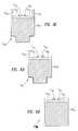
- FIG. 13shows an exploded top perspective view of a corner of an embodiment of a spatial light modulator of the present invention.
- FIG. 14shows a cell having the sub-hinge design of FIG. 10A configured in an array of similarly structured cells.
- opticalmeans related to any electromagnetic frequencies, not just frequencies in the visible range.
- an “optically transmissive substrate”is a substrate which is transmissive to electromagnetic propagation of a working frequency, whether in the visible range or not.
- FIG. 1A top perspective view of a corner of an embodiment of a micro-mechanical spatial light modulator 10 (hereinafter, “SLM 10 ”) of this invention is shown in FIG. 1 .
- SLM 10may include pixel cells of any configuration or array size. However, for clarity, only four pixel cells 12 , 12 a , 12 b and 12 c in a two by two grid configuration are shown in FIG. 1 .
- the pixel cells 12 , 12 a , 12 b and 12 chave a pixel pitch of, for example, 12 microns. “Pixel pitch” is defined as the distance between like portions of neighboring pixel cells.
- Reflective deflectable elementse.g., mirrors 48 , 48 a , 48 b and 48 c ), each corresponding to a respective pixel cell 12 , 12 a , 12 b and 12 c , are attached to the lower surface 14 of an optically transmissive substrate 20 in an undeflected position.
- mirrors 48 , 48 a , 48 b and 48 care visible through optically transmissive substrate 20 in FIG. 1 .
- light blocking aperture layers 22between the mirrors 48 , 48 a , 48 b or 48 c and the optically transmissive substrate 20 , are represented only by dashed lines so as to show underlying hinges 50 , 50 a , 50 b and 50 c .
- the distance separating neighboring mirrorsmay be, for example, 0.5 microns or less.
- FIGS. 2A-2FOne process for fabricating SLM 10 is illustrated in bottom perspective view in FIGS. 2A-2F. For clarity, only the fabrication of pixel cell 12 is described. However, from this description, it will be apparent that pixel cells 12 a , 12 b , 12 c and the other pixel cells in SLM 10 may be fabricated at the same time and in the same manner as pixel cell 12 is fabricated.
- the optically transmissive substrate 20is made of materials which can withstand subsequent processing temperatures.
- the optically transmissive substrate 20may be, for example, a 4 inch quartz wafer 500 microns thick. Such quartz wafers are widely available from, for example, Hoya Corporation U.S.A at 960 Rincon Circle, San Jose, Calif. 95131.
- a light blacking layer(e.g., a 50 nm thick tungsten layer) is deposited and patterned to form the light-blocking aperture layer 22 .
- the aperture layer 22is made out of an opaque material (e.g., tungsten) which remains stable during subsequent fabrication steps.
- the tungstenmay be deposited using, for example, well-known sputtering techniques.
- a pattern of photoresistis formed over the aperture layer 22 using well-known photolithographic processes.
- Aperture layer 22is then etched using a Drytek 100 plasma etcher.
- a mixture of 50% by volume SF 6 and 50% by volume C 2 CLF 5is introduced into the reaction chamber of the etcher at a rate of 300 sccm (150 sccm for HF 6 and 150 sccm for C 2 CIF 5 ).
- Etchingoccurs at a pressure of approximately 100 mTorr with the power setting on the etcher at 500 watts until the optically transmissive substrate 20 is exposed (approximately one minute). After etching, the remaining photoresist is removed using a conventional oxygen plasma strip. Patterning described hereinafter may be similarly performed.
- an optically transmissive protective layer 24(e.g., an approximately 94 nm thick 7%-by-weight phosphorus-doped silicon dioxide) is next deposited as a passivation layer.
- the reflective deflectable element (mirror 48 )is to be connected to optically transmissive substrate 20 through protective layer 24 .
- the silicon dioxide protective layer 24may be deposited, for example, by LPCVD processes in the quartz tube of a Tylan furnace at approximately 400° C. and 250 mTorr for approximately 5 minutes. SiH 4 , O 2 , and PH 3 are introduced into the chamber at rates of 28, 115 and 7 sccm, respectively. The phosphorous-doped silicon dioxide is then reflowed at 1100° C. for 20 minutes in a steam environment.
- a sacrificial layer 26(e.g., an approximately 0.6 ⁇ m thick amorphous silicon layer), which will eventually be removed as described hereinafter, is deposited on the protective layer 24 .
- the amorphous silicon layermay be deposited using LPCVD processes in, for example, the quartz tube of a Tylan furnace.
- the SLM 10is exposed in the quartz tube at approximately 670° C. and 200 mTorr for 135 minutes.
- a composition of SiH 4 and H 2is introduced into the quartz tube at a flow rate of 246 sccm (146 sccm for SiH 4 and 100 sccm for H 2 ).
- Holes 25are patterned through sacrificial amorphous silicon layer 26 by selective anisotropic etching by using, for example, patterned plasma etching in a 50% SF 6 and 50% C 2 ClF 5 (by volume) environment until a portion of protective layer 24 is exposed through sacrificial layer 26 .
- patterned plasma etchingin a 50% SF 6 and 50% C 2 ClF 5 (by volume) environment until a portion of protective layer 24 is exposed through sacrificial layer 26 .
- Such etchingmay occur in the reaction chamber of a Drytek 100 plasma etcher.
- the gas compositionis introduced at a rate of 100 sccm (50 sccm for SF 6 and 50 sccm for C 2 ClF 2 ), and a pressure of 150 mTorr. Typically, it takes approximately 4.5 minutes to expose the portion of protective layer 24 through sacrificial layer 26 under these conditions.
- a mirror structural support layer 28for example an approximately 138 nm thick low-stress silicon nitride layer, is deposited and patterned to form mirror 48 and motion stop 49 .
- Mirror 48is a substantially rigid plate.
- the low stress silicon nitride layermay be deposited, for example, in a quartz tube of a Tylan furnace by using LPCVD processes at approximately 785° C. and 250 mTorr for approximately 36 minutes. Deposition occurs, for example, by introducing SiCl 2 H 2 and NH 3 into the quartz tube at 165 sccm and 32 sccm, respectively.
- the silicon nitridemay be etched using an AMT 8100 hexagonal-electrode plasma etcher powered at 1200 watts.
- the etch gasesfor example, O 2 and CHF 3 , are introduced into the reaction chamber at respective flow rates of 6 sccm and 85 sccm, respectively, with an etch period of 17 minutes. Under these conditions, the polysilicon to silicon nitride selectivity ratio is approximately 1:6.
- a hinge layer 30(e.g., an approximately 40 nm thick layer of low-stress silicon nitride) is then grown and patterned to additionally define the torsion hinge 50 (a top view of this pattern can be seen in FIG. 8 A). At least a portion of hinge 50 contacts protective layer 24 through holes 25 to define supports 51 (FIGS. 2 D- 2 F).
- the hinge 50operates by “torsion” which means that the hinge 50 is twisted by applying torque about the longitudinal direction of the hinge 50 .
- Hinge 50may be, for example, approximately 0.5 microns wide.
- the thin layer of low stress silicon nitride for the hinge layer 30is deposited in a quartz tube of a Tylan furnace using an LPCVD process.
- SiCl 2 H 2 and NH 3are introduced into the quartz tube at a flow rate of, for example, 165 sccm and 32 sccm, respectively.
- the depositionoccurs, for example, at a temperature of 785° C. and at a pressure of 250 mTorr for 11 minutes.
- the sacrificial layer 26is then partially removed using an isotropic etch process.
- the etch processis isotropic so that portions of the sacrificial layer 26 are removed from underneath the mirror 48 and hinge 50 .
- the sacrificial layer 26 that is not underneath mirror 48 and hinge 50is removed.
- significant portions of the sacrificial layer 26 underneath mirror 48 and hinge 50remain due to the protection of mirror 48 and hinge 50 . Therefore, after the partial etch, sacrificial layer 26 continues to support mirror 48 and hinge 50 and prevents airborne particulates from lodging underneath mirror 48 and hinge 50 during further fabrication steps described hereinafter.
- One suitable isotropic etch processis by exposure to a plasma etching process in the reaction chamber of a Drytek 100 plasma etcher. Approximately 100% SF 6 is introduced into the reaction chamber at a flow rate of approximately 50 sccm with the power setting on the etcher set at 375 watts. Etching occurs for approximately 100 seconds at room temperature (however, the plasma generates heat), and a pressure of approximately 150 mTorr. In this process, the selectivity ratio of silicon to silicon nitride is approximately 6:1.
- horizontal surfaces (e.g., mirror structural support layer 28 , hinge layer 30 , and portions of protective layer 24 ) of the SLM 10are then coated with a conductive and reflective layer 32 (e.g., approximately 30 nm thick layer of aluminum) which is optically reflective.
- a conductive and reflective layer 32e.g., approximately 30 nm thick layer of aluminum
- Some vertical surfacese.g., the vertical surface of hinge 50 proximate the mirror 48
- the portions of reflective layer 32 on hinge layer 30 and the vertical surfacesare not shown in FIG. 2 E.
- Such a reflective layer 32may be deposited by, for example, evaporating aluminum downwardly at an angle such that the horizontal vector of the angle is from mirror 48 to motion stop 49 . With this angle, no metal (aluminum) exists on protective layer 24 at the point where motion stop 49 contacts protective layer 24 because motion stop 49 shields this surface from metal deposition. Note that the protective layer 24 is exposed due to the partial etching of sacrificial layer 26 described above. The evaporation may occur, for example, in the reaction chamber of an e-gun thermal evaporator at a deposition rate of one nanometer per second.
- Spacers 44are provided on the optically transmissive substrate. Spacers 44 are, for example, composed of Hoechst-Delanese AZ4330-RS photoresist, spun on at 5000 rpm for 30 seconds, exposed and patterned to form spacers 44 using conventional photolithographic techniques, then hard baked at 233° C. for 1 hour to give increased structural rigidity.
- the mirrors 48 a , 48 b and 48 care fully released from optically transmissive substrate 20 , except at hinge supports 51 and 51 , with a second isotropic etch, for example, a xenon diflouride etch process, which completely removes the sacrificial layer 26 .
- This etchingis performed at approximately 4 Torr in an approximately 100% xenon diflouride environment for approximately 20 minutes at room temperature. Under these conditions the selectivity of this etching process is over a hundred to one.
- the optically transmissive substrate 20 with the mirror array attached theretois now ready to bond to a circuit substrate 34 (e.g., a semiconductor substrate) containing addressing circuitry 36 , as shown in cross section in FIG. 3 A.
- a circuit substrate 34e.g., a semiconductor substrate
- Spacers 44are bonded to the circuit substrate 34 to hold optically transmissive substrate 20 apart from, but in close proximity to, circuit substrate 34 .
- planar optical elementssuch as two dielectric layers 70 and 72 (FIG. 2F) having a different index of refraction are deposited as mirror structural support layer 28 .
- This stack of dielectric layersmay reflect light or filter out specific frequency ranges.
- a layer of silicon dioxide (optical index of 1.46) deposited on top of a layer of silicon nitride (with an optical index of 2.0)will enhance the reflectivity of, for example, aluminum reflective layer 32 with a reflectivity of 92% to 95% over much of the optical spectrum if the silicon nitride layer is 68 nm thick and the silicon dioxide layer is 96 nm thick.
- optically transmissive substrate 20is bonded to the circuit substrate 34 .
- the substrates 20 and 34are optically aligned and held together, and can be glued together with epoxy dispensed around the edge of circuit substrate 34 .
- top substrate 20is optically transmissive
- alignmentcan be accomplished easily by aligning a pattern on the optically transmissive substrate 20 to a pattern on the circuitry substrate 34 .
- the mirror 48may be isolated from airborne particulates.
- a bottom electrode 42(e.g., a 500 nm thick aluminum bottom electrode) of cell 12 is shown connecting to addressing circuitry 36 through contact 43 .
- the active bottom electrode 42should be physically located higher than the rest of the circuit components 36 and interconnects.
- the bottom electrode 42interacts with the overhanging mirror 48 through electrostatic forces.
- FIG. 3AThe operation of the above-described embodiment is shown in FIG. 3 A and FIG. 3 B.
- the mirror 48In FIG. 3A, the mirror 48 is undeflected.
- an incoming light beam, from a light source 64 , obliquely incident to SLM 10passes through the optically transmissive substrate 20 and is reflected by the flat mirrors 48 and partially reflected by aperture layer 22 .
- the angle of the outgoing light beam 58is thus also oblique to the optically transmissive substrate 20 .
- the outgoing light beammay be received by, for example, an optical dump 78 .
- the incorporation of the aperture layer 22 into the optically transmissive substrate 20is a technique to eliminate unwanted light scattering from the underlying hinge 50 .
- FIG. 3 BCell 12 with a voltage bias applied between the mirror 48 and the bottom electrode 42 applied is shown in FIG. 3 B.
- the mirror 48is deflected due to electrostatic attraction. Because of the design of the hinge 50 , the free end of the mirror 48 is deflected towards the circuit substrate 34 .
- hinge 50may be more flexible than mirror 48 such that the application of force causes substantially all of the bending to be in hinge 50 . This may be accompished by making hinge layer 30 much thinner than mirror structural support layer 28 as described above.
- the deflection of the mirror 48deflects the outgoing light beam 58 , by a significant angle, into the imaging optics 66 .
- mirror 48The motion of mirror 48 is limited by motion stop 49 contacting the protective layer 24 deposited on optically transmissive substrate 20 (see FIG. 3B) so that mirror 48 does not contact the circuit substrate 34 . Since contact does not occur, the electrically connected mirrors 48 , 48 a , 48 b and 48 c remain at the same potential. Also, there is no charge injection and welding between the mirror 48 and the electrode 42 which can result in sticking.
- the motion stop 49may extend (for example, approximately 3.3 microns) from the pivot axis of hinge 50 .
- FIG. 4 and FIG. 5The full electromechanical characteristics of the modulator are further elucidated in FIG. 4 and FIG. 5 .
- deflection angle ⁇ of the mirror 48is plotted against the voltage bias and hysteresis is observed.
- V snapsnapping voltage
- the restoring mechanical force of the hinges 50can no longer balance the electrostatic force and the mirror 48 snaps toward the electrode 42 of the circuit substrate 34 (see line 402 of FIG. 4) until motion stop 49 contacts optically transmissive substrate 20 .
- the voltagemust be lowered substantially below the snapping voltage (see line 403 of FIG. 4) to V release (e.g., approximately 5.6 volts) in order for the mirror 48 to return towards its undeflected position (see line 404 of FIG. 4 ).
- V releasee.g., approximately 5.6 volts
- the mirror 48would be an electromechanically bistable device between voltages V release and V snap .
- mirror 48 deflectionacts as a latch.
- each electrode 42 in each given rowmay be electrically connected while each mirror 48 in each given column is electrically connected.
- the applied voltage biasis at an intermediate voltage (e.g., 6.2 volts) between V release and V snap .
- the deflection of mirror 48represents a one binary state (e.g., a binary one) if the mirror 48 is deflected at line 403 and the other binary state (e.g., a binary zero) if the mirror is deflected at line 401 .
- this intermediate voltagedoes not uniquely determine the state of mirror 48 deflection.
- the electrode 42 voltage of the addressed pixel cell rowis altered to increase (or decrease to turn off) the applied bias voltage.
- the mirror 48 voltage of the addressed pixel cell columnis also altered to increase (or decrease to turn off) the applied bias voltage.
- the applied bias voltageincreases (or decreases to turn off), but is still between V release and V snap . Therefore, the binary states do not change for the unaddressed pixel cells that are in the same row and column as the addressed pixel cell.
- both the electrode 42 and mirror 48 voltageshave been altered to increase (or decrease to turn off) the applied bias voltage.
- This increaseis greater than V snap (or the decrease is less than V release to turn off the addressed pixel) and thus the addressed pixel cell is on (or off).
- the driver circuitsmay be placed along the periphery of the device or off chip.
- each electrode 42has a driving circuit (such as a transistor in a DRAM configuration)
- connecting mirrors in groupscould increase addressing efficiency. This may be accomplished either with connections at the periphery of the mirror array, or by depositing pillars connecting the mirrors to the circuit substrate at pixel locations. Since the electrostatic force depends only on the total voltage between conductive and reflective layer 32 and bottom electrode 42 , a negative voltage applied to a mirror group (via reflective layer 32 ) reduces the operating voltage of the corresponding electrodes thus reducing the voltage requirement of SLM 10 . It is desirable, for example, to keep the-operating voltage below 5V because 5V switching capability is standard to the semiconductor industry. In addition, the amount of charge needed to bias each electrode of the addressed pixel is smaller than an embodiment in which all mirrors are held at ground. Thus the time required to program the addressed pixel cell is relatively fast.
- the upward directed mechanical force(or the downward directed electrostatic force) dominates and the mirror 48 deflects back up (or down) to the equilibrium point ⁇ E .
- the tilt of the mirror 48is controlled.
- the motion stops 49 described aboveare made of hard is materials such as silicon nitride. These hard materials have potentially longer lifetimes than metal structures. Motion stops 49 also have a limited contact area with the optically transmissive substrate 20 and therefore reduce sticking forces. By keeping the motion stops 49 at the same potential as the reflective layer 32 with which they come into contact, electrical potential differences that lead to welding can also be avoided. Snapping and thus physical contact between motion stops 49 and optically transmissive substrate 20 can be avoided entirely by keeping V ⁇ V b .
- the SLM 10If the SLM 10 is operated at voltages past the snapping point, it can be operated in a digital manner using either active addressing (i.e., a separate transistor drives electrode 42 at each pixel location), or using passive addressing (i.e., only one driver circuit for each row or column), by exploiting the electromechanical bistability mentioned earlier. If SLM 10 operates at voltages greater than V snap deflection along line 403 may represent one binary state while all other deflections represent the other binary state.
- the SLM 10is operated at voltages below the snapping point, it can be operated in an analog fashion using active addressing. For example, for different deflection angles ⁇ , a different intensity of light may be reflected to imaging optics 66 if light source 64 emits rays from a wide range of locations.
- the use of high quality mechanical materials described aboveresults in good uniformity over the pixel array, and makes analog operation practical.
- the mirror 48 deflectionwill then be proportional to the charge stored at each corresponding electrode. Operation below the snapping point also has the advantage of preventing mechanical contact during operation, eliminating possible sticking problems.
- the addressing voltageis set to the level required for electrostatic-force-based mirror deflection for those electrodes where mirror deflection is required. After the mirrors in question have deflected, the voltage required to hold in the deflected position is less than that required for the actual deflection. This is because the gap between the deflected mirror and the addressing electrode is already smaller than when the mirror is in the process of being deflected. Therefore, in the stage after the active addressing stage, (called the “hold stage”, for example), the addressing voltage level could be reduced from its original level without substantially affecting the state of the mirrors.
- One advantage of having a hold stage voltageis that the undeflected mirrors are now also subject to a smaller electrostatic attractive force than before, and they therefore attain a position closer to the zero-deflected position. This improves the optical contrast ratio between the deflected mirrors and the undeflected mirrors.
- FIG. 6 A and FIG. 6 BAn electrical schematic of a memory array portion of addressing circuitry 36 is shown in FIG. 6 A and FIG. 6 B. If active addressing is employed, an addressing scheme embodied in the circuitry of FIG. 6A can be used to address each pixel cell of the SLM 10 individually. Substrates 20 and 34 are not shown in FIG. 6A, and the mirror 48 and bottom electrode 42 are drawn symbolically. The scheme is identical to that used for a DRAM (dynamic random access memory). Each pixel cell 12 , 12 a , 12 b and 12 c is driven by a respective NMOS transistor 68 , 68 a , 68 b and 68 c . For example, if pixel cell 12 is to be addressed, electrode 42 is charged as follows.
- the state of the corresponding column of pixels(containing pixel cells 12 and 12 c ) is set by holding the corresponding bit line 62 at the appropriate is bias voltage for the desired mirror deflection.
- the biasis relative to the mirrors 48 , which are connected to a common voltage such as ground.
- the corresponding word line 60is then pulsed low-high-low (i.e., NMOS transistor 68 is temporarily opened) and the voltage value is stored as charge between the bottom electrode 42 and mirror 48 .
- An additional capacitormay be placed electrically in parallel to the mirror-electrode combination to insure that enough charge is stored to overcome leakage.
- SRAMstatic random access memory
- pixel cell 12is addressed by applying a voltage representing a binary one on the corresponding bit line 62 .
- the voltageis sufficient to charge electrode 42 and deflect mirror 48 .
- a voltage representing a binary zerois present on the other corresponding bit line 62 (bar).
- the corresponding word line 60is selected by asserting a voltage sufficient to open transistors 69 a and 69 b .
- the input to inverter 69 c and the output from inverter 69 drepresent a binary zero.
- the output from inverter 69 c and the input to inverter 69 drepresents a binary one. With transistor 69 a open, electrode 42 is charged through bit line 62 .
- Possible circuitryincludes, but is not limited to, storage buffers to store time sequential pixel information at each pixel; and electronic circuitry to compensate for possible non-uniformity of mirror/electrode separation by driving the electrodes at varying voltage levels.
- an SLM 10can be made to have an operating voltage of only a few volts.
- the angular torsion modulus of hinge 50may be, for example, approximately 3.3 ⁇ 10 ⁇ 14 Newton meters per degree of rotation.
- the voltage at which the addressing circuitry must operatecan be made even lower by maintaining the mirror 48 potential negative (or positive), as referenced to the circuit ground (the bias voltage). For example, in the negative bias case, this has the effect of shifting the hysteresis curve of FIG.
- the maximum negative bias voltageis ⁇ V release .
- the negative voltagemay be asserted to mirror 48 by, for example, closing switch 76 coupling the mirror 48 to a voltage source 74 configured to assert a negative voltage (see pixel cell 12 of FIG. 6 A).
- FIG. 7shows a top view of a reasonably contiguous mirror array having a spacer 44 in the middle.
- the mirror arrayincludes 56 mirrors 48 , 48 a to 48 z , 48 aa to 48 az , 48 ba , 48 bb and 48 bc .
- optically transmissive substrate 20 and circuit substrate 34are not shown and each mirror 48 is represented as a square.
- Spacer 44is centered among mirrors 48 aa , 48 ab , 48 ai and 48 aj , each mirror having an edge coplanar with a corresponding edge of spacer 44 as shown in FIG. 7 .
- FIG. 8Ashows a top plan view of pixel cells 12 and 12 a of the SLM 10 created by the process described with reference to FIGS. 2A-2D.
- the mirrors 48 and 48 arotate around the axis defined by the thin hinges 50 and 50 a .
- Mirror 48 and 48 a motionis limited by the motion stops 49 and 49 a , which move towards and eventually hit the optically transmissive substrate 20 to which the mirrors 48 and 48 a are attached (see FIG. 3 B).
- the diagonal linesrepresent the area which includes a relatively thick silicon nitride layer as compared to the thinner hinges. This reinforcement mechanically stiffens mirrors 48 and 48 a while retaining flexibility in hinges 50 and 50 a . Similar reinforcement is seen in FIGS. 8B-8E.
- FIGS. 8A-8Dshow variations in which motion stop 49 and mirror 48 are substantially coplanar.
- One embodimenthas two motion stops 49 8B is shown in FIG. 8 B.
- hinges 50 8Care connected directly to motion stops 49 8C .
- FIGS. 8C and 8Dare similar except that FIG. 8D shows only one motion stop 49 8D
- FIG. 8Eshows supports 51 8E that are adjacent.
- Pixel cell 12 8E of FIG. 8Ehas no motion stops at all and is most useful if SLM 10 operates only at below V snap .
- hinges 50 8F and 50 8Goperate by flexure and not by torsion.
- “Flexure”means that the ends of hinges 50 8B and 50 8G are fixed and that angular deflection of mirrors 48 8F and 48 8G causes hinge 50 8F and 50 8G to deflect angularly at a middle portion of hinges 50 8F and 50 8G , thereby causing hinges 50 8F and 50 8G to stretch along the longitudinal direction of hinges 50 8F and 50 8G .
- hinge supports 51 8F and 51 8Gwhich tie hinges 50 8F and 50 8G down to optically transmissive substrate 20 (FIGS. 1, 2 A, 2 B, 2 C, 2 D, 2 E, 2 F, 3 A, 3 B, 9 A, 9 B, 9 C, 9 D, 10 A, 10 B, 10 C, 11 A, 11 B, 1 C, 12 and 13 ).
- hinges 50 8F and 50 8Gbend longitudinally and not torsionally.
- the mechanical restoring forcewill increase with faster-than-linear dependence on deflection, as the strain in primarily tensile.
- a hinge 50 8F or 50 8G with this characteristicmight be useful when the mirror 48 is operated in an analog manner, since the snapping angle (and thus V snap ) will be increased.
- the hinge 50 8His a cantilever design, also operating by flexion and not by torsion.
- FIGS. 9A-9D and FIG. 10 AA second fabrication process to produce the micromechanical SLM 10 of this invention is illustrated in cross-section in FIGS. 9A-9D and FIG. 10 A.
- This processuses multiple silicon nitride layers to achieve a mirror-type structure with a higher aperture ratio (fraction of optically active area) than is possible with the process outlined in FIGS. 2A-2F. This is partly because the mirror stop 49 10A (FIG. 10A) and mirror 48 10A (FIG. 10A) lie in different planes.
- Optically transmissive substrate 20is made of materials such as guartz which can withstand subsequent processing temperatures.
- the deposition of the light-blocking aperture layer 22 and protective layer 24shown in FIGS. 1, 2 A, 2 B and 2 C, has been skipped but could be added as the first step of the process.
- Sacrificial layer 26 10A(e.g., an approximately 0.5 micron thick, LPCVD-grown amorphous silicon layer) is deposited. After holes 25 10A are patterned through to optically transmissive substrate 20 as seen in FIG. 9A, a motion stop layer (e.g., a 150 nm thick LPCVD-grown low-stress silicon nitride layer) is deposited and patterned to form the motion stop 49 10 A having a sharp contact tip 90 .
- a motion stop layere.g., a 150 nm thick LPCVD-grown low-stress silicon nitride layer
- a hinge layer(e.g., a 40 nm thick layer of low-stress silicon nitride) is grown and then patterned to define the torsion hinges 50 10A as seen in FIG. 9B.
- a second sacrificial layer 27is deposited (e.g., an approximately 0.5 micron thick, LPCVD-grown amorphous silicon layer), and patterned so that a hole 25 c reaches down to the hinge 50 10A (FIG. 9 C).
- This second sacrificial layer 27 10Acould be polished with commonly known chemical mechanical polishing (CMP) techniques to achieve a flat surface for subsequent film depositions.
- CMPchemical mechanical polishing
- the mirror structural support layer 28 10Awill feature enhanced flatness thus improved reflective uniformity and improved system contrast and brightness. Finally, an approximately 138 nm thick silicon nitride mirror structural support layer 28 10A is deposited and patterned to form the substantially rigid mirror plate (FIG. 9 D).
- sacrificial layers 26 10A and 27are partially removed using an isotropic (e.g., a xenon diflouride gas etch; the 100% SF 6 plasma process refered to earlier may also be used) etch process, and the entire structure is coated with, for example, a very thin layer (30 nm) of aluminum (reflective layer 32 10A of FIG. 10A) which is both highly reflective and serves to electrically connect the mirrors together as described above.
- an isotropice.g., a xenon diflouride gas etch; the 100% SF 6 plasma process refered to earlier may also be used
- a sub-hinge structureis fabricated in which a hinge 50 10A , which may be transparent, is disposed between the optically transmissive substrate 20 and the mirror 48 .
- FIGS. 10A-10Cshow embodiments of the sub-hinge structure fabricated using the process above. For clarity, SLM's 10 10A-10D are rotated 90 degrees so that hinges 50 10A-10D may be seen.
- FIG. 10Ashows a cell 12 10A with a torsion hinge 50 10A and one motion stop 49 10A centrally located. This device is shown to scale in an array of similarly structure cells in FIG. 14 .
- FIG. 10Bshows an embodiment with two motion stops 49 10B .
- FIG. 10Cshows a device that uses two ribbon-type hinges 49 10C , which also inherently provide the “motion stop” functionality in two ways.
- hinges 50 10Cwhich may be straight in the undeflected position, take on an S shape due to torque applied by mirror 48 10C .
- the hinges 50 10Cstretch, as well as bend.
- the mechanical restoring force for mirror 48 10Cincreases at greater than a linear rate with reference to angular deflection.
- This non-linear qualityis one way by which hinges 50 10C function provide “motion stop” functionality even without contacting the optically transmissive substrate 20 .
- a second way that “motion stop” functionality is achieved with this structureis by contact between the mirror 48 10C and hinges 50 10C .
- FIG. 10Dshows yet another embodiment of a torsion hinge device, for which the step of depositing the motion stop layer can be eliminated, since it does not make use of separately fabricated motion stops.
- contacts 51 10Dare formed through holes in a first sacrificial layer.
- a ribbon hinge 50 10Dis formed on the first sacrificial layer.
- a second sacrificial layeris formed over the hinge 50 10D and the first sacrificial layer and formed with a hole which exposes a central portion of hinge 50 10D .
- Contact 51 ⁇is formed through the hole and a single layer forming mirror 48 10D and motion stop 49 10D is deposited on top of the second sacrificial layer. The two sacrificial layers are then removed to free mirror 48 10D and motion stop 49 10D .
- FIGS. 11A-11C and FIG. 12A third fabrication process to produce the micro-mechanical spatial light modulator (SLM) of this invention is illustrated in cross-section in FIGS. 11A-11C and FIG. 12 .
- This processalso uses multiple silicon nitride layers to achieve a mirror-type structure with a higher aperture ratio (fraction of optically active area) than is possible with the process outlined in FIG. 2 .
- Optically transmissive substrate 20is made of a material such as quartz which can withstand subsequent processing temperatures. In this process, the deposition of the light-blocking aperture layer 22 , protective layer 24 has been omitted from the process, but could be added as the first step in the process.
- the optically transmissive substrate 20is patterned and etched so that small bumps 111 are formed as contact points, as seen in FIG. 1 A.
- a 0.5 ⁇ m thick LPCVD-grown amorphous silicon sacrificial layer 26 12is deposited, which will eventually be removed.
- a second sacrificial layer 27 12is deposited, and patterned so that hole 29 ⁇ reaches down to the mirror plate 28 , and so that holes 2912 reach down to bumps 111 .
- An approximately 40 nm thick low-stress silicon nitride hinge layer 29 12is then grown and patterned to define the torsion hinges as seen in FIG. 1 C.
- the sacrificial layers 26 12 and 27 12are partially removed using a xenon diflouride isotropic etch process having an etch selectivity of over 100 to 1 (a 100% SF 6 plasma process may also be used), and the entire structure is coated with a very thin layer (30 nm) of aluminum which is both highly reflective and serves to electrically connect the mirrors together. Finally the mirrors are fully released with a second xenon diflouride etch process, completely removing the sacrificial layer 26 12 . The mirrors are now ready to be joined with a semiconductor substrate containing addressing circuitry, using the same substrate bonding techniques described earlier in reference to FIG. 2 and FIG. 3 .
- FIG. 12shows an embodiment of the structure fabricated using the process above.
- Supports 51 12are formed by the silicon nitride hinge layer deposition through holes 29 12 .
- Hinge 50 12is formed of hinge layer 29 12 .
- Mirror 48 12is the mirror plate 28 12 shown in FIG. 11 B. This mirror is attached to hinge 50 12 via support 51 ⁇ .
- the mirror 48 12is separated from optically transmissive substrate 20 in the undeflected position due to supports 51 12 .
- a single square mirroris not the only possible reflective deflectable element 48 possible; other designs, such as a cloverleaf or grating-like design are possible. For example, a row of skinny mirrors all deflecting in unison can form a switchable diffraction grating. It is also feasible that the reflective deflectable element is a metal-coated membrane. The deflectable element design could also be made so that one part of the element moves away from the lower substrate instead of towards it. Mirror elements can also be designed to deflect in more than one direction, i.e. have more than one controllable degree of freedom.
- additional structuremay be added to the circuit substrate.
- protruding bumpscan be fabricated to reduce the total surface area actually in contact.
- the bumpsare preferably at the same electrical potential as the mirror to avoid welding on contact.
- a conducting transparent layersuch as indium tin oxide, can be deposited before the protective layer 24 . A bias applied between the conducting transparent layer and the mirrors will actively pull the mirrors to the top substrate 20 and reset them to their off state.
- the DRAM, SRAM, and passive addressing schemes described above, as well as latch devices commonly known to the art,may all perform the addressing function.
- the circuit substratemay be transparent, for example, quartz.
- transistorsmay be made from polysilicon, as compared to crystalline silicon.
- the aperture layer 22may be further modified to comprise any binary optical pattern.
- other planar optical componentscan be integrated into the optically transmissive substrate 20 , at either the top surface 16 or bottom surface 14 of optically transmissive substrate 20 .
- Some of the many possible structuresinclude color filters composed of one or a stack of layers, micro-lenses, and color-dispersive or diffractive features. See for example Jahns and Huang, “Planar Integration of Free-Space Optical components” Applied optics, vol. 28, No. 9, May 1, 1989.
- the ability to integrate this optical functionality into the optically transmissive substratecan increase achievable contrast ratio and lowers cost by reducing the cost of free-space optics at the system level.
- the mirror platesthemselves can incorporate optical functionality beyond simple reflectivity.
- the mirrorscan be comprised of multiple substantially transparent layers to add filtering capability or to enhance reflectivity of certain wavelengths as compared to others. This is useful, for example, as a means to balance color deficiencies of the optical system, such as the spectrum of an illuminating lamp.
- Chemical-mechanical polishingcan be added at several stages during the fabrication process, for example after the protective layer has been deposited on top of the patterned aperture layer, or after the mirror layer has been deposited, in order to make the optically active area of the mirror as flat as possible.
- micro-mechanical elementsmany material substitutions are possible for the micro-mechanical elements: one possibility is the use of another type of ceramic (e.g. silicon dioxide) for the mirror, or even making the mirror completely out of a metal (e.g. an aluminum alloy).
- the sacrificial layer materialsuch as silicon dioxide. Silicon could also be used instead of tungsten as the grid material. This would make the process more compatible with silicon nitride deposition facilities that are used for CMOS chip production. The grid and associated protective layer may also be left out entirely.
- silicone.g., LPCVD polycrystalline silicon
- deflectable elementse.g. mirrors
- silicon dioxidee.g., LPCVD grown
- the silicon dioxidemay be etched away with hydrofluoric acid, and drying may be accomplished using well-known critical-point-drying techniques to facilitate stiction-free mirror release.
- the spacerscan also be made from a wide variety of materials, including various polymers, oxides, or metals.
- the SLM 10 of this inventionis a device that exhibits many desirable properties, including high resolution, high optical efficiency, high contrast ratio or modulation depth, and high mechanical reliability.
- the SLM 10has application in a wide variety of areas, including projection display systems.
- Low switching voltages and the innovative design of the SLM 10enable standard CMOS circuitry to be used as the addressing mechanism.
- the deflectable elementsthemselves can also be manufactured using standard processes available in silicon CMOS fabrication facilities, on a separate substrate. Both substrates can be fabricated using relatively gross features and less than state-of-the-art facilities. These factors make the SLM 10 easy and inexpensive, to manufacture.
Landscapes
- Physics & Mathematics (AREA)
- General Physics & Mathematics (AREA)
- Optics & Photonics (AREA)
- Mechanical Light Control Or Optical Switches (AREA)
Abstract
Description
Claims (57)
Priority Applications (13)
| Application Number | Priority Date | Filing Date | Title |
|---|---|---|---|
| US09/624,591US6356378B1 (en) | 1995-06-19 | 2000-07-24 | Double substrate reflective spatial light modulator |
| US10/043,703US6538800B2 (en) | 1995-06-19 | 2002-01-09 | Reflective spatial light modulator with deflectable elements formed on a light transmissive substrate |
| US10/153,138US6690502B2 (en) | 1995-06-19 | 2002-05-20 | Double substrate reflective spatial light modulator with self-limiting micro-mechanical elements |
| US10/305,631US6952301B2 (en) | 1995-06-19 | 2002-11-26 | Spatial light modulators with light blocking and absorbing areas |
| US10/748,899US6798561B2 (en) | 1995-06-19 | 2003-12-29 | Double substrate reflective spatial light modulator with self-limiting micro-mechanical elements |
| US10/948,871US6947200B2 (en) | 1995-06-19 | 2004-09-24 | Double substrate reflective spatial light modulator with self-limiting micro-mechanical elements |
| US10/969,380US7138693B2 (en) | 1995-06-19 | 2004-10-19 | Barrier layers for microelectromechanical systems |
| US11/001,806US7023607B2 (en) | 1995-06-19 | 2004-12-01 | Double substrate reflective spatial light modulator with self-limiting micro-mechanical elements |
| US11/001,807US7012733B2 (en) | 1995-06-19 | 2004-12-01 | Double substrate reflective spatial light modulator with self-limiting micro-mechanical elements |
| US11/090,800US7009754B2 (en) | 1995-06-19 | 2005-03-24 | Double substrate reflective spatial light modulator with self-limiting micro-mechanical elements |
| US11/089,920US7027207B2 (en) | 1995-06-19 | 2005-03-24 | Double substrate reflective spatial light modulator with self-limiting micro-mechanical elements |
| US11/089,692US6975444B2 (en) | 1995-06-19 | 2005-03-24 | Double substrate reflective spatial light modulator with self-limiting micro-mechanical elements |
| US11/340,319US7403324B2 (en) | 1995-06-19 | 2006-01-25 | Double substrate reflective spatial light modulator with self-limiting micro-mechanical elements |
Applications Claiming Priority (5)
| Application Number | Priority Date | Filing Date | Title |
|---|---|---|---|
| US32295P | 1995-06-19 | 1995-06-19 | |
| US08/665,380US5835256A (en) | 1995-06-19 | 1996-06-18 | Reflective spatial light modulator with encapsulated micro-mechanical elements |
| US09/160,361US6046840A (en) | 1995-06-19 | 1998-09-24 | Double substrate reflective spatial light modulator with self-limiting micro-mechanical elements |
| US09/437,586US6172797B1 (en) | 1995-06-19 | 1999-11-09 | Double substrate reflective spatial light modulator with self-limiting micro-mechanical elements |
| US09/624,591US6356378B1 (en) | 1995-06-19 | 2000-07-24 | Double substrate reflective spatial light modulator |
Related Parent Applications (1)
| Application Number | Title | Priority Date | Filing Date |
|---|---|---|---|
| US09/437,586ContinuationUS6172797B1 (en) | 1995-06-19 | 1999-11-09 | Double substrate reflective spatial light modulator with self-limiting micro-mechanical elements |
Related Child Applications (2)
| Application Number | Title | Priority Date | Filing Date |
|---|---|---|---|
| US10/005,308ContinuationUS6969635B2 (en) | 1995-06-19 | 2001-12-03 | Methods for depositing, releasing and packaging micro-electromechanical devices on wafer substrates |
| US10/043,703ContinuationUS6538800B2 (en) | 1995-06-19 | 2002-01-09 | Reflective spatial light modulator with deflectable elements formed on a light transmissive substrate |
Publications (1)
| Publication Number | Publication Date |
|---|---|
| US6356378B1true US6356378B1 (en) | 2002-03-12 |
Family
ID=27356649
Family Applications (13)
| Application Number | Title | Priority Date | Filing Date |
|---|---|---|---|
| US09/160,361Expired - LifetimeUS6046840A (en) | 1995-06-19 | 1998-09-24 | Double substrate reflective spatial light modulator with self-limiting micro-mechanical elements |
| US09/437,586Expired - LifetimeUS6172797B1 (en) | 1995-06-19 | 1999-11-09 | Double substrate reflective spatial light modulator with self-limiting micro-mechanical elements |
| US09/624,591Expired - LifetimeUS6356378B1 (en) | 1995-06-19 | 2000-07-24 | Double substrate reflective spatial light modulator |
| US10/043,703Expired - Fee RelatedUS6538800B2 (en) | 1995-06-19 | 2002-01-09 | Reflective spatial light modulator with deflectable elements formed on a light transmissive substrate |
| US10/153,138Expired - LifetimeUS6690502B2 (en) | 1995-06-19 | 2002-05-20 | Double substrate reflective spatial light modulator with self-limiting micro-mechanical elements |
| US10/748,899Expired - LifetimeUS6798561B2 (en) | 1995-06-19 | 2003-12-29 | Double substrate reflective spatial light modulator with self-limiting micro-mechanical elements |
| US10/948,871Expired - LifetimeUS6947200B2 (en) | 1995-06-19 | 2004-09-24 | Double substrate reflective spatial light modulator with self-limiting micro-mechanical elements |
| US11/001,806Expired - LifetimeUS7023607B2 (en) | 1995-06-19 | 2004-12-01 | Double substrate reflective spatial light modulator with self-limiting micro-mechanical elements |
| US11/001,807Expired - LifetimeUS7012733B2 (en) | 1995-06-19 | 2004-12-01 | Double substrate reflective spatial light modulator with self-limiting micro-mechanical elements |
| US11/090,800Expired - LifetimeUS7009754B2 (en) | 1995-06-19 | 2005-03-24 | Double substrate reflective spatial light modulator with self-limiting micro-mechanical elements |
| US11/089,920Expired - LifetimeUS7027207B2 (en) | 1995-06-19 | 2005-03-24 | Double substrate reflective spatial light modulator with self-limiting micro-mechanical elements |
| US11/089,692Expired - LifetimeUS6975444B2 (en) | 1995-06-19 | 2005-03-24 | Double substrate reflective spatial light modulator with self-limiting micro-mechanical elements |
| US11/340,319Expired - LifetimeUS7403324B2 (en) | 1995-06-19 | 2006-01-25 | Double substrate reflective spatial light modulator with self-limiting micro-mechanical elements |
Family Applications Before (2)
| Application Number | Title | Priority Date | Filing Date |
|---|---|---|---|
| US09/160,361Expired - LifetimeUS6046840A (en) | 1995-06-19 | 1998-09-24 | Double substrate reflective spatial light modulator with self-limiting micro-mechanical elements |
| US09/437,586Expired - LifetimeUS6172797B1 (en) | 1995-06-19 | 1999-11-09 | Double substrate reflective spatial light modulator with self-limiting micro-mechanical elements |
Family Applications After (10)
| Application Number | Title | Priority Date | Filing Date |
|---|---|---|---|
| US10/043,703Expired - Fee RelatedUS6538800B2 (en) | 1995-06-19 | 2002-01-09 | Reflective spatial light modulator with deflectable elements formed on a light transmissive substrate |
| US10/153,138Expired - LifetimeUS6690502B2 (en) | 1995-06-19 | 2002-05-20 | Double substrate reflective spatial light modulator with self-limiting micro-mechanical elements |
| US10/748,899Expired - LifetimeUS6798561B2 (en) | 1995-06-19 | 2003-12-29 | Double substrate reflective spatial light modulator with self-limiting micro-mechanical elements |
| US10/948,871Expired - LifetimeUS6947200B2 (en) | 1995-06-19 | 2004-09-24 | Double substrate reflective spatial light modulator with self-limiting micro-mechanical elements |
| US11/001,806Expired - LifetimeUS7023607B2 (en) | 1995-06-19 | 2004-12-01 | Double substrate reflective spatial light modulator with self-limiting micro-mechanical elements |
| US11/001,807Expired - LifetimeUS7012733B2 (en) | 1995-06-19 | 2004-12-01 | Double substrate reflective spatial light modulator with self-limiting micro-mechanical elements |
| US11/090,800Expired - LifetimeUS7009754B2 (en) | 1995-06-19 | 2005-03-24 | Double substrate reflective spatial light modulator with self-limiting micro-mechanical elements |
| US11/089,920Expired - LifetimeUS7027207B2 (en) | 1995-06-19 | 2005-03-24 | Double substrate reflective spatial light modulator with self-limiting micro-mechanical elements |
| US11/089,692Expired - LifetimeUS6975444B2 (en) | 1995-06-19 | 2005-03-24 | Double substrate reflective spatial light modulator with self-limiting micro-mechanical elements |
| US11/340,319Expired - LifetimeUS7403324B2 (en) | 1995-06-19 | 2006-01-25 | Double substrate reflective spatial light modulator with self-limiting micro-mechanical elements |
Country Status (1)
| Country | Link |
|---|---|
| US (13) | US6046840A (en) |
Cited By (210)
| Publication number | Priority date | Publication date | Assignee | Title |
|---|---|---|---|---|
| US6480646B2 (en)* | 2000-05-12 | 2002-11-12 | New Jersey Institute Of Technology | Micro-mirror and actuator with extended travel range |
| US6529310B1 (en)* | 1998-09-24 | 2003-03-04 | Reflectivity, Inc. | Deflectable spatial light modulator having superimposed hinge and deflectable element |
| US6538800B2 (en)* | 1995-06-19 | 2003-03-25 | Reflectivity, Inc. | Reflective spatial light modulator with deflectable elements formed on a light transmissive substrate |
| WO2003079091A1 (en)* | 2002-03-15 | 2003-09-25 | Micronic Laser Systems Ab | An adressing method of moveable microelements in a spatial light modulator (slm) for pattering of a workpiece |
| US20030214639A1 (en)* | 2000-08-03 | 2003-11-20 | Satyadev Patel | Micromirrors with OFF-angle electrodes and stops |
| WO2003103022A1 (en) | 2002-05-28 | 2003-12-11 | Silicon Light Machines Corporation | Integrated driver process flow |
| US6664786B2 (en) | 2001-07-30 | 2003-12-16 | Rockwell Automation Technologies, Inc. | Magnetic field sensor using microelectromechanical system |
| US20030234994A1 (en)* | 2002-06-19 | 2003-12-25 | Pan Shaoher X. | Reflective spatial light modulator |
| US20040004753A1 (en)* | 2002-06-19 | 2004-01-08 | Pan Shaoher X. | Architecture of a reflective spatial light modulator |
| US20040006576A1 (en)* | 2002-07-03 | 2004-01-08 | Sean Colbath | Systems and methods for providing multimedia information management |
| US6690178B2 (en) | 2001-10-26 | 2004-02-10 | Rockwell Automation Technologies, Inc. | On-board microelectromechanical system (MEMS) sensing device for power semiconductors |
| JP2004102249A (en)* | 2002-07-19 | 2004-04-02 | Canon Inc | Micro movable body |
| US20040070815A1 (en)* | 2002-10-11 | 2004-04-15 | Aubuchon Christopher M. | Micromirror systems with open support structures |
| US20040069742A1 (en)* | 2002-06-19 | 2004-04-15 | Pan Shaoher X. | Fabrication of a reflective spatial light modulator |
| US20040070813A1 (en)* | 2002-10-11 | 2004-04-15 | Aubuchon Christopher M. | Micromirror systems with electrodes configured for sequential mirror attraction |
| US20040095659A1 (en)* | 2002-11-19 | 2004-05-20 | Samsung Electronics Co., Ltd. | Micromirror actuator and method of manufacturing the same |
| US6741383B2 (en)* | 2000-08-11 | 2004-05-25 | Reflectivity, Inc. | Deflectable micromirrors with stopping mechanisms |
| US6749308B1 (en)* | 1999-12-28 | 2004-06-15 | Robert Bosch Gmbh | Micromirror |
| US6756310B2 (en) | 2001-09-26 | 2004-06-29 | Rockwell Automation Technologies, Inc. | Method for constructing an isolate microelectromechanical system (MEMS) device using surface fabrication techniques |
| US20040125281A1 (en)* | 2002-12-25 | 2004-07-01 | Wen-Jian Lin | Optical interference type of color display |
| US6761829B2 (en) | 2001-04-26 | 2004-07-13 | Rockwell Automation Technologies, Inc. | Method for fabricating an isolated microelectromechanical system (MEMS) device using an internal void |
| US6762868B2 (en)* | 2000-11-16 | 2004-07-13 | Texas Instruments Incorporated | Electro-optical package with drop-in aperture |
| US6768628B2 (en) | 2001-04-26 | 2004-07-27 | Rockwell Automation Technologies, Inc. | Method for fabricating an isolated microelectromechanical system (MEMS) device incorporating a wafer level cap |
| US20040165249A1 (en)* | 2003-02-24 | 2004-08-26 | Aubuchon Christopher M. | Micromirror systems with concealed multi-piece hinge structures |
| US20040165250A1 (en)* | 2003-02-24 | 2004-08-26 | Aubuchon Christopher M. | Multi-tilt micromirror systems with concealed hinge structures |
| US6794271B2 (en)* | 2001-09-28 | 2004-09-21 | Rockwell Automation Technologies, Inc. | Method for fabricating a microelectromechanical system (MEMS) device using a pre-patterned bridge |
| US6798312B1 (en) | 1999-09-21 | 2004-09-28 | Rockwell Automation Technologies, Inc. | Microelectromechanical system (MEMS) analog electrical isolator |
| US20040189142A1 (en)* | 2003-03-25 | 2004-09-30 | Knieser Michael J. | Microelectromechanical isolating circuit |
| US6803755B2 (en) | 1999-09-21 | 2004-10-12 | Rockwell Automation Technologies, Inc. | Microelectromechanical system (MEMS) with improved beam suspension |
| US20040212868A1 (en)* | 2003-04-22 | 2004-10-28 | Taiwan Semiconductor Manufacturing Co. | Trench-embeded mirror structure for double substrate spatial light modulator |
| US6815243B2 (en) | 2001-04-26 | 2004-11-09 | Rockwell Automation Technologies, Inc. | Method of fabricating a microelectromechanical system (MEMS) device using a pre-patterned substrate |
| US20040226909A1 (en)* | 2003-04-23 | 2004-11-18 | Jiann-Tyng Tzeng | Reflective spatial light modulator mirror device manufacturing process and layout method |
| US20040240033A1 (en)* | 2002-06-19 | 2004-12-02 | Pan Shaoher X. | High fill ratio reflective spatial light modulator with hidden hinge |
| US6870659B2 (en) | 2002-10-11 | 2005-03-22 | Exajoule, Llc | Micromirror systems with side-supported mirrors and concealed flexure members |
| US20050104144A1 (en)* | 2003-11-19 | 2005-05-19 | Xhp Microsystems, Inc. | Method and apparatus to reduce parasitic forces in electro-mechanical systems |
| US6906850B2 (en)* | 2000-12-28 | 2005-06-14 | Texas Instruments Incorporated | Capacitively coupled micromirror |
| US20050128564A1 (en)* | 2003-10-27 | 2005-06-16 | Pan Shaoher X. | High contrast spatial light modulator and method |
| US20050157376A1 (en)* | 2002-11-26 | 2005-07-21 | Huibers Andrew G. | Spatial light modulators with light blocking/absorbing areas |
| US20050162727A1 (en)* | 2004-01-24 | 2005-07-28 | Fusao Ishii | Micromirrors with support walls |
| US20050170546A1 (en)* | 2001-03-15 | 2005-08-04 | Patel Satyadev R. | Metod for making a micromechanical device by using a sacrificial substrate |
| US20050174628A1 (en)* | 2002-06-19 | 2005-08-11 | Miradia Inc. | Memory cell dual protection |
| US6950223B2 (en)* | 2003-01-15 | 2005-09-27 | Reflectivity, Inc | Multiple hinge MEMS device |
| US20050213092A1 (en)* | 2003-09-26 | 2005-09-29 | Mackinnon Nicholas B | Apparatus and methods relating to enhanced spectral measurement systems |
| US20050212738A1 (en)* | 2004-03-06 | 2005-09-29 | Brian Gally | Method and system for color optimization in a display |
| US20050213181A1 (en)* | 2003-09-26 | 2005-09-29 | Mackinnon Nicholas B | Apparatus and methods relating to precision control of illumination exposure |
| US20050249966A1 (en)* | 2004-05-04 | 2005-11-10 | Ming-Hau Tung | Method of manufacture for microelectromechanical devices |
| US20050255666A1 (en)* | 2004-05-11 | 2005-11-17 | Miradia Inc. | Method and structure for aligning mechanical based device to integrated circuits |
| US20050275930A1 (en)* | 2004-06-15 | 2005-12-15 | Satyadev Patel | Micromirror array assembly with in-array pillars |
| US20050286112A1 (en)* | 2004-06-23 | 2005-12-29 | Satyadev Patel | Micromirror having offset addressing electrode |
| US20060012850A1 (en)* | 2004-06-30 | 2006-01-19 | Nathanson Harvey C | Side spring micro-mirror |
| US20060023286A1 (en)* | 2004-07-28 | 2006-02-02 | Miradia Inc. | Method and apparatus for a reflective spatial light modulator with a flexible pedestal |
| US20060028708A1 (en)* | 1994-05-05 | 2006-02-09 | Miles Mark W | Method and device for modulating light |
| US20060035439A1 (en)* | 2004-08-13 | 2006-02-16 | Ching-Heng Po | Method of forming a micromechanical structure |
| US20060061760A1 (en)* | 2004-09-22 | 2006-03-23 | Ushiodenki Kabushiki Kaisha | Absorption spectrometric analysis microchip |
| US20060066557A1 (en)* | 2004-09-27 | 2006-03-30 | Floyd Philip D | Method and device for reflective display with time sequential color illumination |
| US20060066586A1 (en)* | 2004-09-27 | 2006-03-30 | Gally Brian J | Touchscreens for displays |
| US20060067600A1 (en)* | 2004-09-27 | 2006-03-30 | Gally Brian J | Display element having filter material diffused in a substrate of the display element |
| US20060066599A1 (en)* | 2004-09-27 | 2006-03-30 | Clarence Chui | Reflective display pixels arranged in non-rectangular arrays |
| US20060066641A1 (en)* | 2004-09-27 | 2006-03-30 | Gally Brian J | Method and device for manipulating color in a display |
| US20060067633A1 (en)* | 2004-09-27 | 2006-03-30 | Gally Brian J | Device and method for wavelength filtering |
| US20060066541A1 (en)* | 2004-09-27 | 2006-03-30 | Gally Brian J | Method and device for manipulating color in a display |
| US20060067649A1 (en)* | 2004-09-27 | 2006-03-30 | Ming-Hau Tung | Apparatus and method for reducing slippage between structures in an interferometric modulator |
| US20060077522A1 (en)* | 2004-09-27 | 2006-04-13 | Manish Kothari | Method and device for compensating for color shift as a function of angle of view |
| US20060077122A1 (en)* | 2004-09-27 | 2006-04-13 | Gally Brian J | Apparatus and method for reducing perceived color shift |
| US20060077510A1 (en)* | 2004-09-27 | 2006-04-13 | Clarence Chui | System and method of illuminating interferometric modulators using backlighting |
| US20060079048A1 (en)* | 2004-09-27 | 2006-04-13 | Sampsell Jeffrey B | Method of making prestructure for MEMS systems |
| US20060077125A1 (en)* | 2004-09-27 | 2006-04-13 | Idc, Llc. A Delaware Limited Liability Company | Method and device for generating white in an interferometric modulator display |
| US20060077153A1 (en)* | 2004-09-27 | 2006-04-13 | Idc, Llc, A Delaware Limited Liability Company | Reduced capacitance display element |
| US20060077149A1 (en)* | 2004-09-27 | 2006-04-13 | Gally Brian J | Method and device for manipulating color in a display |
| US20060077124A1 (en)* | 2004-09-27 | 2006-04-13 | Gally Brian J | Method and device for manipulating color in a display |
| US20060077514A1 (en)* | 2004-09-27 | 2006-04-13 | Sampsell Jeffrey B | System and method of reducing color shift in a display |
| US20060077154A1 (en)* | 2004-09-27 | 2006-04-13 | Gally Brian J | Optical films for directing light towards active areas of displays |
| US20060077512A1 (en)* | 2004-09-27 | 2006-04-13 | Cummings William J | Display device having an array of spatial light modulators with integrated color filters |
| US20060082858A1 (en)* | 2004-10-19 | 2006-04-20 | Peter Heureux | Micromirror array device and a method for making the same |
| US20060082860A1 (en)* | 2004-10-19 | 2006-04-20 | Andrew Huibers | Asymmetric spatial light modulator in a package |
| US20060082856A1 (en)* | 2004-10-19 | 2006-04-20 | Satyadev Patel | Spatial light modulators with non-uniform pixels |
| US7034984B2 (en) | 2002-06-19 | 2006-04-25 | Miradia Inc. | Fabrication of a high fill ratio reflective spatial light modulator with hidden hinge |
| US20060087717A1 (en)* | 2004-06-18 | 2006-04-27 | Miradia Inc. | Mirror structure with single crystal silicon cross-member |
| US20060132383A1 (en)* | 2004-09-27 | 2006-06-22 | Idc, Llc | System and method for illuminating interferometric modulator display |
| US20060148121A1 (en)* | 2005-01-03 | 2006-07-06 | Miradia Inc. | Method and structure for forming an integrated spatial light modulator |
| US20060152795A1 (en)* | 2005-01-07 | 2006-07-13 | Miradia Inc. | Electrical contact method and structure for deflection devices formed in an array configuration |
| US20060152794A1 (en)* | 2005-01-07 | 2006-07-13 | Miradia Inc. | Method and structure for reducing parasitic influences of deflection devices on spatial light modulators |
| US20060187523A1 (en)* | 2003-10-27 | 2006-08-24 | Pan Shaoher X | Fabricating micro devices using sacrificial materials |
| US20060207964A1 (en)* | 2005-03-17 | 2006-09-21 | Taiwan Semiconductor Manufacturing Co., Ltd. | Method for releasing a micromechanical structure |
| US20060250337A1 (en)* | 1999-10-05 | 2006-11-09 | Miles Mark W | Photonic MEMS and structures |
| US20060274400A1 (en)* | 1995-11-06 | 2006-12-07 | Miles Mark W | Method and device for modulating light with optical compensation |
| US20060274397A1 (en)* | 2005-06-01 | 2006-12-07 | Miradia Inc. | Co-planar surface and torsion device mirror structure and method of manufacture for optical displays |
| US20060274398A1 (en)* | 2005-06-03 | 2006-12-07 | Chen-Jean Chou | Interferometric modulator with internal polarization and drive method |
| US20060285192A1 (en)* | 2005-06-15 | 2006-12-21 | Miradia Inc. | Method and structure of patterning landing pad structures for spatial light modulators |
| US7184195B2 (en) | 2005-06-15 | 2007-02-27 | Miradia Inc. | Method and structure reducing parasitic influences of deflection devices in an integrated spatial light modulator |
| US7202989B2 (en) | 2005-06-01 | 2007-04-10 | Miradia Inc. | Method and device for fabricating a release structure to facilitate bonding of mirror devices onto a substrate |
| US20070121118A1 (en)* | 2005-05-27 | 2007-05-31 | Gally Brian J | White interferometric modulators and methods for forming the same |
| US20070134896A1 (en)* | 2005-12-14 | 2007-06-14 | Spatial Photonics, Inc. | Method for fabricating a micro structure |
| US20070177247A1 (en)* | 1998-04-08 | 2007-08-02 | Miles Mark W | Method and device for modulating light with multiple electrodes |
| US20070177244A1 (en)* | 2006-01-30 | 2007-08-02 | Taiwan Semiconductor Manufacturing Co., Ltd. | Method and system for patterning alignment marks on a transparent substrate |
| US20070189654A1 (en)* | 2006-01-13 | 2007-08-16 | Lasiter Jon B | Interconnect structure for MEMS device |
| US20070196040A1 (en)* | 2006-02-17 | 2007-08-23 | Chun-Ming Wang | Method and apparatus for providing back-lighting in an interferometric modulator display device |
| US20070247704A1 (en)* | 2006-04-21 | 2007-10-25 | Marc Mignard | Method and apparatus for providing brightness control in an interferometric modulator (IMOD) display |
| US7295363B2 (en) | 2005-04-08 | 2007-11-13 | Texas Instruments Incorporated | Optical coating on light transmissive substrates of micromirror devices |
| US20080003784A1 (en)* | 2006-06-28 | 2008-01-03 | Pan Shaoher X | Low temperature fabrication of conductive micro structures |
| US20080013154A1 (en)* | 2004-09-27 | 2008-01-17 | Idc, Llc | System and method for multi-level brightness in interferometric modulation |
| US20080055707A1 (en)* | 2006-06-28 | 2008-03-06 | Lior Kogut | Support structure for free-standing MEMS device and methods for forming the same |
| US20080063796A1 (en)* | 2003-10-23 | 2008-03-13 | Spatial Photonics, Inc. | High resolution spatial light modulation |
| US7349141B2 (en) | 2004-09-27 | 2008-03-25 | Idc, Llc | Method and post structures for interferometric modulation |
| US20080080043A1 (en)* | 2004-09-27 | 2008-04-03 | Idc, Llc | Conductive bus structure for interferometric modulator array |
| US20080094690A1 (en)* | 2006-10-18 | 2008-04-24 | Qi Luo | Spatial Light Modulator |
| US20080100900A1 (en)* | 2006-10-27 | 2008-05-01 | Clarence Chui | Light guide including optical scattering elements and a method of manufacture |
| US20080106782A1 (en)* | 1994-05-05 | 2008-05-08 | Idc, Llc | System and method for a mems device |
| US20080110855A1 (en)* | 2004-09-27 | 2008-05-15 | Idc, Llc | Methods and devices for inhibiting tilting of a mirror in an interferometric modulator |
| US20080112039A1 (en)* | 2004-02-03 | 2008-05-15 | Idc, Llc | Spatial light modulator with integrated optical compensation structure |
| US20080160171A1 (en)* | 2006-12-29 | 2008-07-03 | United Technologies Corporation | Electron beam physical vapor deposition apparatus and processes for adjusting the feed rate of a target and manufacturing a multi-component condensate free of lamination |
| US20080180956A1 (en)* | 2007-01-30 | 2008-07-31 | Qualcomm Mems Technologies, Inc. | Systems and methods of providing a light guiding layer |
| US20080186581A1 (en)* | 2007-02-01 | 2008-08-07 | Qualcomm Incorporated | Modulating the intensity of light from an interferometric reflector |
| US20080203054A1 (en)* | 2007-02-27 | 2008-08-28 | Spatial Photonics, Inc. | Planarization of a layer over a cavity |
| US7420725B2 (en) | 2004-09-27 | 2008-09-02 | Idc, Llc | Device having a conductive light absorbing mask and method for fabricating same |
| US20080226929A1 (en)* | 2006-01-18 | 2008-09-18 | Qualcomm Mems Technologies, Inc. | Silicon-rich silicon nitrides as etch stop in mems manufacture |
| US20080239455A1 (en)* | 2007-03-28 | 2008-10-02 | Lior Kogut | Microelectromechanical device and method utilizing conducting layers separated by stops |
| US20080260242A1 (en)* | 2006-06-22 | 2008-10-23 | Tidal Photonics Inc. | Apparatus and methods for measuring and controlling illumination for imaging objects, performances and the like |
| US20080266333A1 (en)* | 2007-01-29 | 2008-10-30 | Qualcomm Mems Technologies, Inc. | Hybrid color synthesis for multistate reflective modular displays |
| US7449284B2 (en) | 2004-05-11 | 2008-11-11 | Miradia Inc. | Method and structure for fabricating mechanical mirror structures using backside alignment techniques |
| US20080288225A1 (en)* | 2007-05-18 | 2008-11-20 | Kostadin Djordjev | Interferometric modulator displays with reduced color sensitivity |
| US20080285112A1 (en)* | 2006-08-30 | 2008-11-20 | Fusao Ishii | Mirror device |
| US20080316568A1 (en)* | 2007-06-21 | 2008-12-25 | Qualcomm Incorporated | Infrared and dual mode displays |
| US7471442B2 (en) | 2006-06-15 | 2008-12-30 | Qualcomm Mems Technologies, Inc. | Method and apparatus for low range bit depth enhancements for MEMS display architectures |
| US20090012361A1 (en)* | 2003-09-26 | 2009-01-08 | Tidal Photonics, Inc. | Apparatus and methods relating to color imaging endoscope systems |
| US20090009444A1 (en)* | 2007-07-03 | 2009-01-08 | Qualcomm Incorporated | Mems devices having improved uniformity and methods for making them |
| US7483200B1 (en)* | 2008-01-14 | 2009-01-27 | Spatial Photonics, Inc. | Multiple stop micro-mirror array display |
| US20090059346A1 (en)* | 2007-08-29 | 2009-03-05 | Qualcomm Incorporated | Interferometric Optical Modulator With Broadband Reflection Characteristics |
| US7502158B2 (en) | 2005-10-13 | 2009-03-10 | Miradia Inc. | Method and structure for high fill factor spatial light modulator with integrated spacer layer |
| US20090073534A1 (en)* | 2007-09-14 | 2009-03-19 | Donovan Lee | Interferometric modulator display devices |
| US20090073539A1 (en)* | 2007-09-14 | 2009-03-19 | Qualcomm Incorporated | Periodic dimple array |
| US20090078316A1 (en)* | 2007-09-24 | 2009-03-26 | Qualcomm Incorporated | Interferometric photovoltaic cell |
| US7515327B2 (en) | 2004-09-27 | 2009-04-07 | Idc, Llc | Method and device for corner interferometric modulation |
| US20090097100A1 (en)* | 2004-09-27 | 2009-04-16 | Idc, Llc | Optical films for controlling angular characteristics of displays |
| US20090101192A1 (en)* | 2007-10-19 | 2009-04-23 | Qualcomm Incorporated | Photovoltaic devices with integrated color interferometric film stacks |
| US20090103166A1 (en)* | 2007-10-23 | 2009-04-23 | Qualcomm Mems Technologies, Inc. | Adjustably transmissive mems-based devices |
| US20090109515A1 (en)* | 2007-10-30 | 2009-04-30 | Spatial Photonics, Inc. | Encapsulated spatial light modulator having large active area |
| US7527998B2 (en) | 2006-06-30 | 2009-05-05 | Qualcomm Mems Technologies, Inc. | Method of manufacturing MEMS devices providing air gap control |
| US20090126777A1 (en)* | 2007-11-16 | 2009-05-21 | Qualcomm Mems Technologies, Inc. | Simultaneous light collection and illumination on an active display |
| US20090147332A1 (en)* | 2007-12-07 | 2009-06-11 | Quanlcomm Incorporated | Decoupled holographic film and diffuser |
| US20090147343A1 (en)* | 2007-12-07 | 2009-06-11 | Lior Kogut | Mems devices requiring no mechanical support |
| US20090151771A1 (en)* | 2007-12-17 | 2009-06-18 | Qualcomm Mems Technologies, Inc. | Photovoltaics with interferometric ribbon masks |
| US7550810B2 (en) | 2006-02-23 | 2009-06-23 | Qualcomm Mems Technologies, Inc. | MEMS device having a layer movable at asymmetric rates |
| US20090159123A1 (en)* | 2007-12-21 | 2009-06-25 | Qualcomm Mems Technologies, Inc. | Multijunction photovoltaic cells |
| US7554714B2 (en) | 2004-09-27 | 2009-06-30 | Idc, Llc | Device and method for manipulation of thermal response in a modulator |
| US7564612B2 (en) | 2004-09-27 | 2009-07-21 | Idc, Llc | Photonic MEMS and structures |
| US20090190373A1 (en)* | 2006-10-06 | 2009-07-30 | Qualcomm Mems Technologies, Inc. | Illumination device with built-in light coupler |
| US20090201571A1 (en)* | 2008-02-12 | 2009-08-13 | Qualcomm Mems Technologies, Inc. | Integrated front light diffuser for reflective displays |
| US20090225395A1 (en)* | 2008-03-07 | 2009-09-10 | Qualcomm Mems Technologies, Inc. | Interferometric modulator in transmission mode |
| US20090225391A1 (en)* | 2001-02-02 | 2009-09-10 | Tidal Photonics, Inc. | Apparatus and methods relating to wavelength conditioning of illumination |
| US20090231672A1 (en)* | 2008-03-12 | 2009-09-17 | Texas Instruments Incorporated | Electrically conductive protection layer and a microelectromechanical device using the same |
| US20090231673A1 (en)* | 2008-03-12 | 2009-09-17 | Texas Instruments Incorporated | Multilayered deformable element with reduced memory properties in a mems device |
| US20090251752A1 (en)* | 2006-10-10 | 2009-10-08 | Qualcomm Mems Technologies, Inc. | Display device with diffractive optics |
| US20090251761A1 (en)* | 2008-04-02 | 2009-10-08 | Kasra Khazeni | Microelectromechanical systems display element with photovoltaic structure |
| US20090257105A1 (en)* | 2008-04-10 | 2009-10-15 | Qualcomm Mems Technologies, Inc. | Device having thin black mask and method of fabricating the same |
| US7612933B2 (en) | 2008-03-27 | 2009-11-03 | Qualcomm Mems Technologies, Inc. | Microelectromechanical device with spacing layer |
| US7612932B2 (en) | 2004-09-27 | 2009-11-03 | Idc, Llc | Microelectromechanical device with optical function separated from mechanical and electrical function |
| US20090273824A1 (en)* | 2007-05-09 | 2009-11-05 | Qualcomm Mems Techologies, Inc. | Electromechanical system having a dielectric movable membrane |
| US20090294766A1 (en)* | 2008-06-02 | 2009-12-03 | Jiou-Kang Lee | Process for Eliminating Delamination between Amorphous Silicon Layers |
| US20090293955A1 (en)* | 2007-11-07 | 2009-12-03 | Qualcomm Incorporated | Photovoltaics with interferometric masks |
| US7630121B2 (en) | 2007-07-02 | 2009-12-08 | Qualcomm Mems Technologies, Inc. | Electromechanical device with optical function separated from mechanical and electrical function |
| US20090323165A1 (en)* | 2008-06-25 | 2009-12-31 | Qualcomm Mems Technologies, Inc. | Method for packaging a display device and the device obtained thereof |
| US20090323154A1 (en)* | 2008-06-25 | 2009-12-31 | Qualcomm Mems Technologies, Inc. | Backlight displays |
| US20090323153A1 (en)* | 2008-06-25 | 2009-12-31 | Qualcomm Mems Technologies, Inc. | Backlight displays |
| US7643199B2 (en) | 2007-06-19 | 2010-01-05 | Qualcomm Mems Technologies, Inc. | High aperture-ratio top-reflective AM-iMod displays |
| US20100004513A1 (en)* | 2003-09-26 | 2010-01-07 | Tidal Photonics, Inc. | Apparatus and methods relating to expanded dynamic range imaging endoscope systems |
| US7649671B2 (en) | 2006-06-01 | 2010-01-19 | Qualcomm Mems Technologies, Inc. | Analog interferometric modulator device with electrostatic actuation and release |
| US20100026727A1 (en)* | 2006-10-06 | 2010-02-04 | Qualcomm Mems Technologies, Inc. | Optical loss structure integrated in an illumination apparatus |
| WO2010014065A1 (en)* | 2008-08-01 | 2010-02-04 | Olympus Corporation | Mirror device |
| US20100039370A1 (en)* | 1996-12-19 | 2010-02-18 | Idc, Llc | Method of making a light modulating display device and associated transistor circuitry and structures thereof |
| US20100053148A1 (en)* | 2008-09-02 | 2010-03-04 | Qualcomm Mems Technologies, Inc. | Light turning device with prismatic light turning features |
| US20100096011A1 (en)* | 2008-10-16 | 2010-04-22 | Qualcomm Mems Technologies, Inc. | High efficiency interferometric color filters for photovoltaic modules |
| US7710636B2 (en) | 2004-09-27 | 2010-05-04 | Qualcomm Mems Technologies, Inc. | Systems and methods using interferometric optical modulators and diffusers |
| US20100109102A1 (en)* | 2005-01-03 | 2010-05-06 | Miradia Inc. | Method and structure for forming a gyroscope and accelerometer |
| US7715085B2 (en) | 2007-05-09 | 2010-05-11 | Qualcomm Mems Technologies, Inc. | Electromechanical system having a dielectric movable membrane and a mirror |
| US20100128337A1 (en)* | 2008-07-11 | 2010-05-27 | Yeh-Jiun Tung | Stiction mitigation with integrated mech micro-cantilevers through vertical stress gradient control |
| US20100157406A1 (en)* | 2008-12-19 | 2010-06-24 | Qualcomm Mems Technologies, Inc. | System and method for matching light source emission to display element reflectivity |
| US7768690B2 (en) | 2008-06-25 | 2010-08-03 | Qualcomm Mems Technologies, Inc. | Backlight displays |
| US20100214645A1 (en)* | 1996-12-19 | 2010-08-26 | Qualcomm Mems Technologies, Inc. | Separable modulator |
| US20100238572A1 (en)* | 2009-03-23 | 2010-09-23 | Qualcomm Mems Technologies, Inc. | Display device with openings between sub-pixels and method of making same |
| US20100245370A1 (en)* | 2009-03-25 | 2010-09-30 | Qualcomm Mems Technologies, Inc. | Em shielding for display devices |
| US20100284055A1 (en)* | 2007-10-19 | 2010-11-11 | Qualcomm Mems Technologies, Inc. | Display with integrated photovoltaic device |
| US7839557B2 (en) | 2004-09-27 | 2010-11-23 | Qualcomm Mems Technologies, Inc. | Method and device for multistate interferometric light modulation |
| US20100302218A1 (en)* | 2009-05-29 | 2010-12-02 | Qualcomm Mems Technologies, Inc. | Illumination devices and methods of fabrication thereof |
| US7852545B2 (en) | 1994-05-05 | 2010-12-14 | Qualcomm Mems Technologies, Inc. | Method and device for modulating light |
| US7855826B2 (en) | 2008-08-12 | 2010-12-21 | Qualcomm Mems Technologies, Inc. | Method and apparatus to reduce or eliminate stiction and image retention in interferometric modulator devices |
| US20110026095A1 (en)* | 2007-07-31 | 2011-02-03 | Qualcomm Mems Technologies, Inc. | Devices and methods for enhancing color shift of interferometric modulators |
| USRE42119E1 (en) | 2002-02-27 | 2011-02-08 | Qualcomm Mems Technologies, Inc. | Microelectrochemical systems device and method for fabricating same |
| US7893919B2 (en) | 2004-09-27 | 2011-02-22 | Qualcomm Mems Technologies, Inc. | Display region architectures |
| US20110063712A1 (en)* | 2009-09-17 | 2011-03-17 | Qualcomm Mems Technologies, Inc. | Display device with at least one movable stop element |
| US7916378B2 (en) | 2007-03-08 | 2011-03-29 | Qualcomm Mems Technologies, Inc. | Method and apparatus for providing a light absorbing mask in an interferometric modulator display |
| US20110075241A1 (en)* | 2009-09-28 | 2011-03-31 | Qualcomm Mems Technologies, Inc. | Interferometric display with interferometric reflector |
| US7936497B2 (en) | 2004-09-27 | 2011-05-03 | Qualcomm Mems Technologies, Inc. | MEMS device having deformable membrane characterized by mechanical persistence |
| US7944599B2 (en) | 2004-09-27 | 2011-05-17 | Qualcomm Mems Technologies, Inc. | Electromechanical device with optical function separated from mechanical and electrical function |
| US7999993B2 (en) | 2004-09-27 | 2011-08-16 | Qualcomm Mems Technologies, Inc. | Reflective display device having viewable display on both sides |
| US8008736B2 (en) | 2004-09-27 | 2011-08-30 | Qualcomm Mems Technologies, Inc. | Analog interferometric modulator device |
| US8164821B2 (en) | 2008-02-22 | 2012-04-24 | Qualcomm Mems Technologies, Inc. | Microelectromechanical device with thermal expansion balancing layer or stiffening layer |
| US8659816B2 (en) | 2011-04-25 | 2014-02-25 | Qualcomm Mems Technologies, Inc. | Mechanical layer and methods of making the same |
| US8670171B2 (en) | 2010-10-18 | 2014-03-11 | Qualcomm Mems Technologies, Inc. | Display having an embedded microlens array |
| US8736939B2 (en) | 2011-11-04 | 2014-05-27 | Qualcomm Mems Technologies, Inc. | Matching layer thin-films for an electromechanical systems reflective display device |
| US8797632B2 (en) | 2010-08-17 | 2014-08-05 | Qualcomm Mems Technologies, Inc. | Actuation and calibration of charge neutral electrode of a display device |
| US8817357B2 (en) | 2010-04-09 | 2014-08-26 | Qualcomm Mems Technologies, Inc. | Mechanical layer and methods of forming the same |
| US8848294B2 (en) | 2010-05-20 | 2014-09-30 | Qualcomm Mems Technologies, Inc. | Method and structure capable of changing color saturation |
| US8872085B2 (en) | 2006-10-06 | 2014-10-28 | Qualcomm Mems Technologies, Inc. | Display device having front illuminator with turning features |
| US8885244B2 (en) | 2004-09-27 | 2014-11-11 | Qualcomm Mems Technologies, Inc. | Display device |
| US8902484B2 (en) | 2010-12-15 | 2014-12-02 | Qualcomm Mems Technologies, Inc. | Holographic brightness enhancement film |
| US8928967B2 (en) | 1998-04-08 | 2015-01-06 | Qualcomm Mems Technologies, Inc. | Method and device for modulating light |
| US8963159B2 (en) | 2011-04-04 | 2015-02-24 | Qualcomm Mems Technologies, Inc. | Pixel via and methods of forming the same |
| US9057872B2 (en) | 2010-08-31 | 2015-06-16 | Qualcomm Mems Technologies, Inc. | Dielectric enhanced mirror for IMOD display |
| US9134527B2 (en) | 2011-04-04 | 2015-09-15 | Qualcomm Mems Technologies, Inc. | Pixel via and methods of forming the same |
Families Citing this family (382)
| Publication number | Priority date | Publication date | Assignee | Title |
|---|---|---|---|---|
| US7123216B1 (en) | 1994-05-05 | 2006-10-17 | Idc, Llc | Photonic MEMS and structures |
| US6952301B2 (en)* | 1995-06-19 | 2005-10-04 | Reflectivity, Inc | Spatial light modulators with light blocking and absorbing areas |
| US6849471B2 (en)* | 2003-03-28 | 2005-02-01 | Reflectivity, Inc. | Barrier layers for microelectromechanical systems |
| US7532377B2 (en) | 1998-04-08 | 2009-05-12 | Idc, Llc | Movable micro-electromechanical device |
| US6872984B1 (en) | 1998-07-29 | 2005-03-29 | Silicon Light Machines Corporation | Method of sealing a hermetic lid to a semiconductor die at an angle |
| US6303986B1 (en) | 1998-07-29 | 2001-10-16 | Silicon Light Machines | Method of and apparatus for sealing an hermetic lid to a semiconductor die |
| US6962419B2 (en) | 1998-09-24 | 2005-11-08 | Reflectivity, Inc | Micromirror elements, package for the micromirror elements, and projection system therefor |
| US6523961B2 (en) | 2000-08-30 | 2003-02-25 | Reflectivity, Inc. | Projection system and mirror elements for improved contrast ratio in spatial light modulators |
| US6337753B1 (en)* | 1998-12-21 | 2002-01-08 | Lucent Technologies Inc. | Optical power equalizer |
| US6191883B1 (en)* | 1998-12-30 | 2001-02-20 | Texas Instruments Incorporated | Five transistor SRAM cell for small micromirror elements |
| US6850353B1 (en) | 1999-06-11 | 2005-02-01 | University Of Hawaii | MEMS optical components |
| US6859299B1 (en) | 1999-06-11 | 2005-02-22 | Jung-Chih Chiao | MEMS optical components |
| AU5480600A (en)* | 1999-06-11 | 2001-01-02 | University Of Hawaii | Reconfigurable quasi-optical unit cells |
| US6396619B1 (en) | 2000-01-28 | 2002-05-28 | Reflectivity, Inc. | Deflectable spatial light modulator having stopping mechanisms |
| US20010040675A1 (en)* | 2000-01-28 | 2001-11-15 | True Randall J. | Method for forming a micromechanical device |
| US6956878B1 (en) | 2000-02-07 | 2005-10-18 | Silicon Light Machines Corporation | Method and apparatus for reducing laser speckle using polarization averaging |
| US7064879B1 (en) | 2000-04-07 | 2006-06-20 | Microsoft Corporation | Magnetically actuated microelectrochemical systems actuator |
| FR2807844B1 (en)* | 2000-04-17 | 2003-05-16 | Commissariat Energie Atomique | MOBILE PIECE OPTICAL SWITCH AND ITS PRODUCTION METHOD, AND OPTICAL BREWING DEVICE USING THE OPTICAL SWITCH |
| JP2001305368A (en)* | 2000-04-21 | 2001-10-31 | Shin Etsu Chem Co Ltd | Manufacturing method of optical waveguide substrate |
| US6709886B2 (en) | 2000-04-25 | 2004-03-23 | Umachines, Inc. | Method of fabricating micromachined devices |
| US6639713B2 (en) | 2000-04-25 | 2003-10-28 | Umachines, Inc. | Silicon micromachined optical device |
| EP2270875B1 (en)* | 2000-04-26 | 2018-01-10 | OSRAM Opto Semiconductors GmbH | Sermiconductor light emitting device and method of manufacturing the same |
| CN1252837C (en)* | 2000-04-26 | 2006-04-19 | 奥斯兰姆奥普托半导体股份有限两合公司 | Light emitting diode chip on GaN substrate and method of manufacturing light emitting diode element using light emitting diode chip on GaN substrate |
| DE10051465A1 (en) | 2000-10-17 | 2002-05-02 | Osram Opto Semiconductors Gmbh | Method for producing a GaN-based semiconductor component |
| KR100708077B1 (en)* | 2000-05-01 | 2007-04-16 | 삼성전자주식회사 | Micromirror Devices for Image Display Devices |
| US6388661B1 (en) | 2000-05-03 | 2002-05-14 | Reflectivity, Inc. | Monochrome and color digital display systems and methods |
| TWI289944B (en) | 2000-05-26 | 2007-11-11 | Osram Opto Semiconductors Gmbh | Light-emitting-diode-element with a light-emitting-diode-chip |
| US6318871B1 (en)* | 2000-06-09 | 2001-11-20 | C Speed Corporation | Optical mirror system with multi-axis rotational control |
| US6611377B1 (en)* | 2000-07-10 | 2003-08-26 | Intel Corporation | Micromechanical diffraction phase grating |
| US6337760B1 (en) | 2000-07-17 | 2002-01-08 | Reflectivity, Inc. | Encapsulated multi-directional light beam steering device |
| US6525864B1 (en)* | 2000-07-20 | 2003-02-25 | Nayna Networks, Inc. | Integrated mirror array and circuit device |
| US6795605B1 (en)* | 2000-08-01 | 2004-09-21 | Cheetah Omni, Llc | Micromechanical optical switch |
| EP1555564A3 (en)* | 2000-08-03 | 2006-10-18 | Reflectivity Inc. | Packaged micromirror array for a projection display |
| US7019376B2 (en)* | 2000-08-11 | 2006-03-28 | Reflectivity, Inc | Micromirror array device with a small pitch size |
| US6873450B2 (en)* | 2000-08-11 | 2005-03-29 | Reflectivity, Inc | Micromirrors with mechanisms for enhancing coupling of the micromirrors with electrostatic fields |
| US7006275B2 (en)* | 2000-08-30 | 2006-02-28 | Reflectivity, Inc | Packaged micromirror array for a projection display |
| US7259510B1 (en)* | 2000-08-30 | 2007-08-21 | Agere Systems Inc. | On-chip vacuum tube device and process for making device |
| WO2002033469A2 (en)* | 2000-10-19 | 2002-04-25 | Axsun Technologies, Inc. | Fabrication process for polysilicon deflectable membrane |
| US6775048B1 (en)* | 2000-10-31 | 2004-08-10 | Microsoft Corporation | Microelectrical mechanical structure (MEMS) optical modulator and optical display system |
| US6647164B1 (en) | 2000-10-31 | 2003-11-11 | 3M Innovative Properties Company | Gimbaled micro-mirror positionable by thermal actuators |
| JP3411014B2 (en)* | 2000-11-02 | 2003-05-26 | 株式会社東芝 | Inductive charge mirror |
| DE10060111C1 (en)* | 2000-12-04 | 2002-07-25 | Siemens Production & Logistics | Optical deflection device |
| KR100416758B1 (en) | 2000-12-05 | 2004-01-31 | 삼성전자주식회사 | Micromirror actuator |
| KR100413793B1 (en)* | 2000-12-05 | 2003-12-31 | 삼성전자주식회사 | Micromirror actuator |
| US6995034B2 (en)* | 2000-12-07 | 2006-02-07 | Reflectivity, Inc | Methods for depositing, releasing and packaging micro-electromechanical devices on wafer substrates |
| US7307775B2 (en)* | 2000-12-07 | 2007-12-11 | Texas Instruments Incorporated | Methods for depositing, releasing and packaging micro-electromechanical devices on wafer substrates |
| US6906847B2 (en)* | 2000-12-07 | 2005-06-14 | Reflectivity, Inc | Spatial light modulators with light blocking/absorbing areas |
| US7116862B1 (en) | 2000-12-22 | 2006-10-03 | Cheetah Omni, Llc | Apparatus and method for providing gain equalization |
| US6711318B2 (en) | 2001-01-29 | 2004-03-23 | 3M Innovative Properties Company | Optical switch based on rotating vertical micro-mirror |
| US7145704B1 (en) | 2003-11-25 | 2006-12-05 | Cheetah Omni, Llc | Optical logic gate based optical router |
| US7339714B1 (en) | 2001-02-02 | 2008-03-04 | Cheetah Omni, Llc | Variable blazed grating based signal processing |
| US6445502B1 (en)* | 2001-02-02 | 2002-09-03 | Celeste Optics, Inc. | Variable blazed grating |
| US7177081B2 (en) | 2001-03-08 | 2007-02-13 | Silicon Light Machines Corporation | High contrast grating light valve type device |
| ES2292720T3 (en)* | 2001-03-09 | 2008-03-16 | Datec Coating Corporation | RESISTIVE COATING AND DRIVER DERIVED FROM SOL-GEL. |
| US6912078B2 (en) | 2001-03-16 | 2005-06-28 | Corning Incorporated | Electrostatically actuated micro-electro-mechanical devices and method of manufacture |
| US6661561B2 (en)* | 2001-03-26 | 2003-12-09 | Creo Inc. | High frequency deformable mirror device |
| US6707591B2 (en) | 2001-04-10 | 2004-03-16 | Silicon Light Machines | Angled illumination for a single order light modulator based projection system |
| US6800210B2 (en)* | 2001-05-22 | 2004-10-05 | Reflectivity, Inc. | Method for making a micromechanical device by removing a sacrificial layer with multiple sequential etchants |
| FR2825479B1 (en)* | 2001-06-01 | 2003-08-29 | Jean Pierre Lazzari | REFLECTION LIGHT MODULATION DEVICE AND MANUFACTURING METHOD THEREOF |
| US6865346B1 (en) | 2001-06-05 | 2005-03-08 | Silicon Light Machines Corporation | Fiber optic transceiver |
| US6600591B2 (en)* | 2001-06-12 | 2003-07-29 | Network Photonics, Inc. | Micromirror array having adjustable mirror angles |
| US6771851B1 (en) | 2001-06-19 | 2004-08-03 | Nayna Networks | Fast switching method for a micro-mirror device for optical switching applications |
| US6747781B2 (en) | 2001-06-25 | 2004-06-08 | Silicon Light Machines, Inc. | Method, apparatus, and diffuser for reducing laser speckle |
| US6782205B2 (en) | 2001-06-25 | 2004-08-24 | Silicon Light Machines | Method and apparatus for dynamic equalization in wavelength division multiplexing |
| JP2003005101A (en)* | 2001-06-26 | 2003-01-08 | Seiko Epson Corp | Light modulation device and method of manufacturing the same |
| JP3852306B2 (en)* | 2001-07-06 | 2006-11-29 | ソニー株式会社 | Method for manufacturing MEMS element, method for manufacturing GLV device, and method for manufacturing laser display |
| JP3760810B2 (en)* | 2001-07-06 | 2006-03-29 | ソニー株式会社 | Light modulation element, GLV device, and laser display |
| US7106377B2 (en)* | 2001-07-25 | 2006-09-12 | Hewlett-Packard Development Company, L.P. | Image capturing device capable of single pixel exposure duration control |
| US20030020958A1 (en)* | 2001-07-30 | 2003-01-30 | Bean Heather Noel | Non-polarizing shutter/CCD module |
| US6538802B2 (en)* | 2001-07-31 | 2003-03-25 | Axsun Technologies, Inc | System and method for tilt mirror calibration due to capacitive sensor drift |
| US7023606B2 (en)* | 2001-08-03 | 2006-04-04 | Reflectivity, Inc | Micromirror array for projection TV |
| US6829092B2 (en) | 2001-08-15 | 2004-12-07 | Silicon Light Machines, Inc. | Blazed grating light valve |
| US6785001B2 (en)* | 2001-08-21 | 2004-08-31 | Silicon Light Machines, Inc. | Method and apparatus for measuring wavelength jitter of light signal |
| US6930364B2 (en)* | 2001-09-13 | 2005-08-16 | Silicon Light Machines Corporation | Microelectronic mechanical system and methods |
| US6956995B1 (en) | 2001-11-09 | 2005-10-18 | Silicon Light Machines Corporation | Optical communication arrangement |
| US7106491B2 (en)* | 2001-12-28 | 2006-09-12 | Texas Instruments Incorporated | Split beam micromirror |
| US6804959B2 (en)* | 2001-12-31 | 2004-10-19 | Microsoft Corporation | Unilateral thermal buckle-beam actuator |
| US6800238B1 (en) | 2002-01-15 | 2004-10-05 | Silicon Light Machines, Inc. | Method for domain patterning in low coercive field ferroelectrics |
| US6794119B2 (en)* | 2002-02-12 | 2004-09-21 | Iridigm Display Corporation | Method for fabricating a structure for a microelectromechanical systems (MEMS) device |
| US7172911B2 (en) | 2002-02-14 | 2007-02-06 | Silex Microsystems Ab | Deflectable microstructure and method of manufacturing the same through bonding of wafers |
| JP3558066B2 (en)* | 2002-02-19 | 2004-08-25 | ソニー株式会社 | MEMS element and its manufacturing method, light modulation element, GLV device and its manufacturing method, and laser display |
| US6856068B2 (en)* | 2002-02-28 | 2005-02-15 | Pts Corporation | Systems and methods for overcoming stiction |
| US6965468B2 (en) | 2003-07-03 | 2005-11-15 | Reflectivity, Inc | Micromirror array having reduced gap between adjacent micromirrors of the micromirror array |
| AU2002256611A1 (en)* | 2002-03-26 | 2003-10-08 | Dicon A/S | Micro light modulator arrangement |
| US6777861B2 (en) | 2002-03-29 | 2004-08-17 | Sony Corporation | Color selector for emissive image display apparatus |
| US6861792B2 (en)* | 2002-03-29 | 2005-03-01 | Sony Corporation | Color separator for emissive display |
| US6947198B2 (en)* | 2002-03-29 | 2005-09-20 | Sony Corporation | Emissive image display apparatus |
| US7053519B2 (en)* | 2002-03-29 | 2006-05-30 | Microsoft Corporation | Electrostatic bimorph actuator |
| US20030184531A1 (en)* | 2002-03-29 | 2003-10-02 | Sony Corporation | GLV engine for image display |
| US6788354B2 (en) | 2002-04-01 | 2004-09-07 | Sony Corporation | Method for making color separator for emissive display |
| US6908791B2 (en)* | 2002-04-29 | 2005-06-21 | Texas Instruments Incorporated | MEMS device wafer-level package |
| GB2388921A (en)* | 2002-05-25 | 2003-11-26 | Alcatel Optronics Uk Ltd | Method of manufacturing an optical actuator and an optical acutator |
| US6728023B1 (en) | 2002-05-28 | 2004-04-27 | Silicon Light Machines | Optical device arrays with optimized image resolution |
| US7054515B1 (en) | 2002-05-30 | 2006-05-30 | Silicon Light Machines Corporation | Diffractive light modulator-based dynamic equalizer with integrated spectral monitor |
| US6822797B1 (en) | 2002-05-31 | 2004-11-23 | Silicon Light Machines, Inc. | Light modulator structure for producing high-contrast operation using zero-order light |
| US6829258B1 (en) | 2002-06-26 | 2004-12-07 | Silicon Light Machines, Inc. | Rapidly tunable external cavity laser |
| US6908201B2 (en) | 2002-06-28 | 2005-06-21 | Silicon Light Machines Corporation | Micro-support structures |
| US6714337B1 (en) | 2002-06-28 | 2004-03-30 | Silicon Light Machines | Method and device for modulating a light beam and having an improved gamma response |
| US6813059B2 (en) | 2002-06-28 | 2004-11-02 | Silicon Light Machines, Inc. | Reduced formation of asperities in contact micro-structures |
| US7057795B2 (en) | 2002-08-20 | 2006-06-06 | Silicon Light Machines Corporation | Micro-structures with individually addressable ribbon pairs |
| US6801354B1 (en) | 2002-08-20 | 2004-10-05 | Silicon Light Machines, Inc. | 2-D diffraction grating for substantially eliminating polarization dependent losses |
| US7781850B2 (en) | 2002-09-20 | 2010-08-24 | Qualcomm Mems Technologies, Inc. | Controlling electromechanical behavior of structures within a microelectromechanical systems device |
| US6712480B1 (en) | 2002-09-27 | 2004-03-30 | Silicon Light Machines | Controlled curvature of stressed micro-structures |
| US7301408B2 (en) | 2002-10-15 | 2007-11-27 | Marvell World Trade Ltd. | Integrated circuit with low dielectric loss packaging material |
| US7768360B2 (en)* | 2002-10-15 | 2010-08-03 | Marvell World Trade Ltd. | Crystal oscillator emulator |
| US7791424B2 (en)* | 2002-10-15 | 2010-09-07 | Marvell World Trade Ltd. | Crystal oscillator emulator |
| US7760039B2 (en)* | 2002-10-15 | 2010-07-20 | Marvell World Trade Ltd. | Crystal oscillator emulator |
| US20060113639A1 (en)* | 2002-10-15 | 2006-06-01 | Sehat Sutardja | Integrated circuit including silicon wafer with annealed glass paste |
| US7729030B2 (en) | 2002-10-21 | 2010-06-01 | Hrl Laboratories, Llc | Optical retro-reflective apparatus with modulation capability |
| US6844959B2 (en)* | 2002-11-26 | 2005-01-18 | Reflectivity, Inc | Spatial light modulators with light absorbing areas |
| US6958846B2 (en)* | 2002-11-26 | 2005-10-25 | Reflectivity, Inc | Spatial light modulators with light absorbing areas |
| US6928207B1 (en) | 2002-12-12 | 2005-08-09 | Silicon Light Machines Corporation | Apparatus for selectively blocking WDM channels |
| US7057819B1 (en) | 2002-12-17 | 2006-06-06 | Silicon Light Machines Corporation | High contrast tilting ribbon blazed grating |
| US6987600B1 (en) | 2002-12-17 | 2006-01-17 | Silicon Light Machines Corporation | Arbitrary phase profile for better equalization in dynamic gain equalizer |
| US6934070B1 (en) | 2002-12-18 | 2005-08-23 | Silicon Light Machines Corporation | Chirped optical MEM device |
| US6927891B1 (en) | 2002-12-23 | 2005-08-09 | Silicon Light Machines Corporation | Tilt-able grating plane for improved crosstalk in 1×N blaze switches |
| US7187484B2 (en)* | 2002-12-30 | 2007-03-06 | Texas Instruments Incorporated | Digital micromirror device with simplified drive electronics for use as temporal light modulator |
| US7274347B2 (en)* | 2003-06-27 | 2007-09-25 | Texas Instruments Incorporated | Prevention of charge accumulation in micromirror devices through bias inversion |
| JP2004219843A (en)* | 2003-01-16 | 2004-08-05 | Seiko Epson Corp | Optical modulator, display device and manufacturing method thereof |
| US7068372B1 (en) | 2003-01-28 | 2006-06-27 | Silicon Light Machines Corporation | MEMS interferometer-based reconfigurable optical add-and-drop multiplexor |
| TW200413810A (en) | 2003-01-29 | 2004-08-01 | Prime View Int Co Ltd | Light interference display panel and its manufacturing method |
| US7286764B1 (en) | 2003-02-03 | 2007-10-23 | Silicon Light Machines Corporation | Reconfigurable modulator-based optical add-and-drop multiplexer |
| US6947613B1 (en) | 2003-02-11 | 2005-09-20 | Silicon Light Machines Corporation | Wavelength selective switch and equalizer |
| US7042622B2 (en)* | 2003-10-30 | 2006-05-09 | Reflectivity, Inc | Micromirror and post arrangements on substrates |
| US6885494B2 (en)* | 2003-02-12 | 2005-04-26 | Reflectivity, Inc. | High angle micro-mirrors and processes |
| US7411717B2 (en)* | 2003-02-12 | 2008-08-12 | Texas Instruments Incorporated | Micromirror device |
| US7483198B2 (en)* | 2003-02-12 | 2009-01-27 | Texas Instruments Incorporated | Micromirror device and method for making the same |
| US7618373B2 (en) | 2003-02-14 | 2009-11-17 | Siemens Medical Solutions Usa, Inc. | Microfabricated ultrasonic transducer array for 3-D imaging and method of operating the same |
| US7087023B2 (en)* | 2003-02-14 | 2006-08-08 | Sensant Corporation | Microfabricated ultrasonic transducers with bias polarity beam profile control and method of operating the same |
| US6922272B1 (en) | 2003-02-14 | 2005-07-26 | Silicon Light Machines Corporation | Method and apparatus for leveling thermal stress variations in multi-layer MEMS devices |
| US7635332B2 (en)* | 2003-02-14 | 2009-12-22 | Siemens Medical Solutions Usa, Inc. | System and method of operating microfabricated ultrasonic transducers for harmonic imaging |
| US7780597B2 (en)* | 2003-02-14 | 2010-08-24 | Siemens Medical Solutions Usa, Inc. | Method and apparatus for improving the performance of capacitive acoustic transducers using bias polarity control and multiple firings |
| US7577431B2 (en) | 2003-02-18 | 2009-08-18 | Roamware, Inc. | Providing multiple MSISDN numbers in a mobile device with a single IMSI |
| US7417782B2 (en)* | 2005-02-23 | 2008-08-26 | Pixtronix, Incorporated | Methods and apparatus for spatial light modulation |
| US6829077B1 (en) | 2003-02-28 | 2004-12-07 | Silicon Light Machines, Inc. | Diffractive light modulator with dynamically rotatable diffraction plane |
| US7027202B1 (en) | 2003-02-28 | 2006-04-11 | Silicon Light Machines Corp | Silicon substrate as a light modulator sacrificial layer |
| US6806997B1 (en) | 2003-02-28 | 2004-10-19 | Silicon Light Machines, Inc. | Patterned diffractive light modulator ribbon for PDL reduction |
| US7391973B1 (en) | 2003-02-28 | 2008-06-24 | Silicon Light Machines Corporation | Two-stage gain equalizer |
| US6922273B1 (en) | 2003-02-28 | 2005-07-26 | Silicon Light Machines Corporation | PDL mitigation structure for diffractive MEMS and gratings |
| US7042611B1 (en) | 2003-03-03 | 2006-05-09 | Silicon Light Machines Corporation | Pre-deflected bias ribbons |
| US7095544B2 (en)* | 2003-03-27 | 2006-08-22 | Taiwan Semiconductor Manufacturing Co., Ltd. | Micromirror and products using the same |
| US7394140B2 (en)* | 2003-05-13 | 2008-07-01 | Texas Instruments Incorporated | Micromirror array device with electrostatically deflectable mirror plates |
| US20040232535A1 (en)* | 2003-05-22 | 2004-11-25 | Terry Tarn | Microelectromechanical device packages with integral heaters |
| JP4338442B2 (en)* | 2003-05-23 | 2009-10-07 | 富士フイルム株式会社 | Manufacturing method of transmissive light modulation element |
| US7397517B2 (en)* | 2003-05-30 | 2008-07-08 | Kazuhiro Ohara | Display system and signal processing using diamond-shaped DMDs |
| WO2004109363A1 (en)* | 2003-06-02 | 2004-12-16 | Miradia Inc. | High fill ratio reflective spatial light modulator with hidden hinge |
| US6980347B2 (en)* | 2003-07-03 | 2005-12-27 | Reflectivity, Inc | Micromirror having reduced space between hinge and mirror plate of the micromirror |
| US7380947B2 (en)* | 2003-07-18 | 2008-06-03 | Texas Instruments Incorporated | Multi-step turn off mode for projection display |
| US6903860B2 (en)* | 2003-11-01 | 2005-06-07 | Fusao Ishii | Vacuum packaged micromirror arrays and methods of manufacturing the same |
| US6862127B1 (en) | 2003-11-01 | 2005-03-01 | Fusao Ishii | High performance micromirror arrays and methods of manufacturing the same |
| US20050094241A1 (en)* | 2003-11-01 | 2005-05-05 | Fusao Ishii | Electromechanical micromirror devices and methods of manufacturing the same |
| US8619352B2 (en)* | 2003-07-29 | 2013-12-31 | Silicon Quest Kabushiki-Kaisha | Projection display system using laser light source |
| TW200506479A (en)* | 2003-08-15 | 2005-02-16 | Prime View Int Co Ltd | Color changeable pixel for an interference display |
| TWI251712B (en)* | 2003-08-15 | 2006-03-21 | Prime View Int Corp Ltd | Interference display plate |
| TW593127B (en)* | 2003-08-18 | 2004-06-21 | Prime View Int Co Ltd | Interference display plate and manufacturing method thereof |
| US7315294B2 (en)* | 2003-08-25 | 2008-01-01 | Texas Instruments Incorporated | Deinterleaving transpose circuits in digital display systems |
| US6982820B2 (en)* | 2003-09-26 | 2006-01-03 | Prime View International Co., Ltd. | Color changeable pixel |
| JP2005121906A (en)* | 2003-10-16 | 2005-05-12 | Fuji Photo Film Co Ltd | Reflection type optical modulation array element and exposure device |
| US20050093134A1 (en)* | 2003-10-30 | 2005-05-05 | Terry Tarn | Device packages with low stress assembly process |
| US6888521B1 (en) | 2003-10-30 | 2005-05-03 | Reflectivity, Inc | Integrated driver for use in display systems having micromirrors |
| US7796321B2 (en)* | 2003-11-01 | 2010-09-14 | Silicon Quest Kabushiki-Kaisha | Mirror device |
| US20090207325A1 (en)* | 2003-11-01 | 2009-08-20 | Naoya Sugimoto | Algorithm for SLM of single hinge type |
| US20090033878A1 (en)* | 2003-11-01 | 2009-02-05 | Akira Shirai | System configurations and methods for controlling image projection apparatuses and mirror device |
| US20090195858A1 (en)* | 2003-11-01 | 2009-08-06 | Naoya Sugimoto | Changing an electrode function |
| US8154474B2 (en)* | 2003-11-01 | 2012-04-10 | Silicon Quest Kabushiki Kaisha | Driving method of memory access |
| US8858811B2 (en)* | 2003-11-01 | 2014-10-14 | Fred Ishii | Method for manufacturing a mirror device by means of a plurality of sacrificial layers |
| US8228595B2 (en)* | 2003-11-01 | 2012-07-24 | Silicon Quest Kabushiki-Kaisha | Sequence and timing control of writing and rewriting pixel memories with substantially lower data rate |
| US7969395B2 (en) | 2003-11-01 | 2011-06-28 | Silicon Quest Kabushiki-Kaisha | Spatial light modulator and mirror device |
| US20090207164A1 (en)* | 2003-11-01 | 2009-08-20 | Naoya Sugimoto | Mirror control within time slot for SLM |
| US8179591B2 (en)* | 2003-11-01 | 2012-05-15 | Silicon Quest Kabushiki-Kaisha | Spatial light modulator and mirror array device |
| US7973994B2 (en)* | 2003-11-01 | 2011-07-05 | Silicon Quest Kabushiki-Kaisha | Spatial light modulator |
| US8194305B2 (en)* | 2003-11-01 | 2012-06-05 | Silicon Quest Kabushiki-Kaisha | Package for micromirror device |
| US20090180038A1 (en)* | 2003-11-01 | 2009-07-16 | Naoya Sugimoto | Mirror control within time slot for SLM |
| US7957050B2 (en) | 2003-11-01 | 2011-06-07 | Silicon Quest Kabushiki-Kaisha | Mirror device comprising layered electrode |
| US7916381B2 (en) | 2003-11-01 | 2011-03-29 | Silicon Quest Kabushiki-Kaisha | Spatial light modulator including drive lines |
| US7304783B2 (en)* | 2003-11-01 | 2007-12-04 | Fusao Ishii | Control of micromirrors with intermediate states |
| US8081371B2 (en)* | 2003-11-01 | 2011-12-20 | Silicon Quest Kabushiki-Kaisha | Spatial light modulator and display apparatus |
| US20090207324A1 (en)* | 2003-11-01 | 2009-08-20 | Naoya Sugimoto | Circuit for SLM's pixel |
| WO2005048174A1 (en)* | 2003-11-10 | 2005-05-26 | Technology Innovations, Llc | Digital imaging assembly and methods thereof |
| US20050106774A1 (en)* | 2003-11-13 | 2005-05-19 | Dmitri Simonian | Surface processes in fabrications of microstructures |
| US20060007515A1 (en)* | 2003-11-13 | 2006-01-12 | Dmitri Simonian | Surface lubrication in microstructures |
| US7274500B2 (en)* | 2003-12-03 | 2007-09-25 | Eastman Kodak Company | Display system incorporating trilinear electromechanical grating device |
| US7514012B2 (en)* | 2004-01-27 | 2009-04-07 | Texas Instruments Incorporated | Pre-oxidization of deformable elements of microstructures |
| US7898144B2 (en)* | 2006-02-04 | 2011-03-01 | Angstrom, Inc. | Multi-step microactuator providing multi-step displacement to a controlled object |
| US7382516B2 (en)* | 2004-06-18 | 2008-06-03 | Angstrom, Inc. | Discretely controlled micromirror with multi-level positions |
| US7580178B2 (en)* | 2004-02-13 | 2009-08-25 | Angstrom, Inc. | Image-guided microsurgery system and method |
| US7350922B2 (en)* | 2004-02-13 | 2008-04-01 | Angstrom, Inc. | Three-dimensional display using variable focal length micromirror array lens |
| US8537204B2 (en)* | 2004-07-08 | 2013-09-17 | Gyoung Il Cho | 3D television broadcasting system |
| US7330297B2 (en)* | 2005-03-04 | 2008-02-12 | Angstrom, Inc | Fine control of rotation and translation of discretely controlled micromirror |
| US7474454B2 (en)* | 2004-06-18 | 2009-01-06 | Angstrom, Inc. | Programmable micromirror motion control system |
| US7751694B2 (en)* | 2004-02-13 | 2010-07-06 | Angstrom, Inc. | Three-dimensional endoscope imaging and display system |
| US7095548B1 (en)* | 2005-07-28 | 2006-08-22 | Angstrom Inc. | Micromirror array lens with free surface |
| US7656573B2 (en)* | 2004-02-28 | 2010-02-02 | Hewlett-Packard Development Company, L.P. | Method and apparatus for controlling a gap between conductors in an electro-mechanical device |
| US7706050B2 (en) | 2004-03-05 | 2010-04-27 | Qualcomm Mems Technologies, Inc. | Integrated modulator illumination |
| US7768571B2 (en)* | 2004-03-22 | 2010-08-03 | Angstrom, Inc. | Optical tracking system using variable focal length lens |
| US7410266B2 (en)* | 2004-03-22 | 2008-08-12 | Angstrom, Inc. | Three-dimensional imaging system for robot vision |
| US7339746B2 (en)* | 2004-03-22 | 2008-03-04 | Angstrom, Inc. | Small and fast zoom system using micromirror array lens |
| US6979893B2 (en)* | 2004-03-26 | 2005-12-27 | Reflectivity, Inc | Packaged microelectromechanical device with lubricant |
| US20050212067A1 (en)* | 2004-03-26 | 2005-09-29 | Robert Duboc | Microelectromechanical devices with lubricants and getters formed thereon |
| US7095545B2 (en)* | 2004-04-02 | 2006-08-22 | Hewlett-Packard Development Company, L.P. | Microelectromechanical device with reset electrode |
| US7619614B2 (en)* | 2004-04-12 | 2009-11-17 | Angstrom, Inc. | Three-dimensional optical mouse system |
| US20070115261A1 (en)* | 2005-11-23 | 2007-05-24 | Stereo Display, Inc. | Virtual Keyboard input system using three-dimensional motion detection by variable focal length lens |
| US20070040924A1 (en)* | 2005-08-19 | 2007-02-22 | Stereo Display, Inc. | Cellular phone camera with three-dimensional imaging function |
| US8049776B2 (en)* | 2004-04-12 | 2011-11-01 | Angstrom, Inc. | Three-dimensional camcorder |
| US7742232B2 (en)* | 2004-04-12 | 2010-06-22 | Angstrom, Inc. | Three-dimensional imaging system |
| US7034982B2 (en)* | 2004-04-13 | 2006-04-25 | Reflectivity, Inc | Method of improving the performance of microstructures |
| US7310242B2 (en)* | 2004-05-21 | 2007-12-18 | General Motors Corporation | Self-shielding high voltage distribution box |
| US7354167B2 (en) | 2004-05-27 | 2008-04-08 | Angstrom, Inc. | Beam focusing and scanning system using micromirror array lens |
| US7777959B2 (en)* | 2004-05-27 | 2010-08-17 | Angstrom, Inc. | Micromirror array lens with fixed focal length |
| US7667896B2 (en) | 2004-05-27 | 2010-02-23 | Angstrom, Inc. | DVD recording and reproducing system |
| US7499065B2 (en)* | 2004-06-11 | 2009-03-03 | Texas Instruments Incorporated | Asymmetrical switching delay compensation in display systems |
| US7483126B2 (en)* | 2004-06-23 | 2009-01-27 | Texas Instruments Incorporated | Performance analyses of micromirror devices |
| US7378287B2 (en)* | 2004-06-23 | 2008-05-27 | Texas Instruments Incorporated | Wafer matching methods for use in assembling micromirror array devices |
| TWI233916B (en)* | 2004-07-09 | 2005-06-11 | Prime View Int Co Ltd | A structure of a micro electro mechanical system |
| EP2246726B1 (en) | 2004-07-29 | 2013-04-03 | QUALCOMM MEMS Technologies, Inc. | System and method for micro-electromechanical operating of an interferometric modulator |
| US6980349B1 (en) | 2004-08-25 | 2005-12-27 | Reflectivity, Inc | Micromirrors with novel mirror plates |
| US7119944B2 (en)* | 2004-08-25 | 2006-10-10 | Reflectivity, Inc. | Micromirror device and method for making the same |
| US7436572B2 (en)* | 2004-08-25 | 2008-10-14 | Texas Instruments Incorporated | Micromirrors and hinge structures for micromirror arrays in projection displays |
| US7019880B1 (en)* | 2004-08-25 | 2006-03-28 | Reflectivity, Inc | Micromirrors and hinge structures for micromirror arrays in projection displays |
| US7675669B2 (en)* | 2004-09-27 | 2010-03-09 | Qualcomm Mems Technologies, Inc. | Method and system for driving interferometric modulators |
| US7373026B2 (en) | 2004-09-27 | 2008-05-13 | Idc, Llc | MEMS device fabricated on a pre-patterned substrate |
| US7184202B2 (en)* | 2004-09-27 | 2007-02-27 | Idc, Llc | Method and system for packaging a MEMS device |
| US7492502B2 (en) | 2004-09-27 | 2009-02-17 | Idc, Llc | Method of fabricating a free-standing microstructure |
| US7368803B2 (en) | 2004-09-27 | 2008-05-06 | Idc, Llc | System and method for protecting microelectromechanical systems array using back-plate with non-flat portion |
| US7369296B2 (en)* | 2004-09-27 | 2008-05-06 | Idc, Llc | Device and method for modifying actuation voltage thresholds of a deformable membrane in an interferometric modulator |
| US7424198B2 (en) | 2004-09-27 | 2008-09-09 | Idc, Llc | Method and device for packaging a substrate |
| US8124434B2 (en) | 2004-09-27 | 2012-02-28 | Qualcomm Mems Technologies, Inc. | Method and system for packaging a display |
| US7545550B2 (en)* | 2004-09-27 | 2009-06-09 | Idc, Llc | Systems and methods of actuating MEMS display elements |
| US7573547B2 (en)* | 2004-09-27 | 2009-08-11 | Idc, Llc | System and method for protecting micro-structure of display array using spacers in gap within display device |
| US7327510B2 (en)* | 2004-09-27 | 2008-02-05 | Idc, Llc | Process for modifying offset voltage characteristics of an interferometric modulator |
| US7701631B2 (en)* | 2004-09-27 | 2010-04-20 | Qualcomm Mems Technologies, Inc. | Device having patterned spacers for backplates and method of making the same |
| US7668415B2 (en) | 2004-09-27 | 2010-02-23 | Qualcomm Mems Technologies, Inc. | Method and device for providing electronic circuitry on a backplate |
| US7684104B2 (en) | 2004-09-27 | 2010-03-23 | Idc, Llc | MEMS using filler material and method |
| US7405861B2 (en) | 2004-09-27 | 2008-07-29 | Idc, Llc | Method and device for protecting interferometric modulators from electrostatic discharge |
| US7446926B2 (en)* | 2004-09-27 | 2008-11-04 | Idc, Llc | System and method of providing a regenerating protective coating in a MEMS device |
| US7405924B2 (en)* | 2004-09-27 | 2008-07-29 | Idc, Llc | System and method for protecting microelectromechanical systems array using structurally reinforced back-plate |
| JP2006098986A (en)* | 2004-09-30 | 2006-04-13 | Fuji Photo Film Co Ltd | Reflection type optical modulation array element and image forming apparatus |
| US7265892B2 (en)* | 2004-10-19 | 2007-09-04 | Texas Instruments Incorporated | Micromirror array devices with light blocking areas |
| US7619807B2 (en)* | 2004-11-08 | 2009-11-17 | Angstrom, Inc. | Micromirror array lens with optical surface profiles |
| US7489434B2 (en) | 2007-05-02 | 2009-02-10 | Angstrom, Inc. | Hybrid micromirror array lens for reducing chromatic aberration |
| US7355677B2 (en)* | 2004-12-09 | 2008-04-08 | Asml Netherlands B.V. | System and method for an improved illumination system in a lithographic apparatus |
| DE102005002967B4 (en)* | 2005-01-21 | 2011-03-31 | Fraunhofer-Gesellschaft zur Förderung der angewandten Forschung e.V. | Method for producing a component with a movable section |
| US9229222B2 (en) | 2005-02-23 | 2016-01-05 | Pixtronix, Inc. | Alignment methods in fluid-filled MEMS displays |
| US9082353B2 (en) | 2010-01-05 | 2015-07-14 | Pixtronix, Inc. | Circuits for controlling display apparatus |
| US7405852B2 (en) | 2005-02-23 | 2008-07-29 | Pixtronix, Inc. | Display apparatus and methods for manufacture thereof |
| US8482496B2 (en) | 2006-01-06 | 2013-07-09 | Pixtronix, Inc. | Circuits for controlling MEMS display apparatus on a transparent substrate |
| US9087486B2 (en) | 2005-02-23 | 2015-07-21 | Pixtronix, Inc. | Circuits for controlling display apparatus |
| US7304786B2 (en) | 2005-02-23 | 2007-12-04 | Pixtronix, Inc. | Methods and apparatus for bi-stable actuation of displays |
| US8519945B2 (en) | 2006-01-06 | 2013-08-27 | Pixtronix, Inc. | Circuits for controlling display apparatus |
| US20060209012A1 (en)* | 2005-02-23 | 2006-09-21 | Pixtronix, Incorporated | Devices having MEMS displays |
| US9158106B2 (en) | 2005-02-23 | 2015-10-13 | Pixtronix, Inc. | Display methods and apparatus |
| US7675665B2 (en) | 2005-02-23 | 2010-03-09 | Pixtronix, Incorporated | Methods and apparatus for actuating displays |
| US7755582B2 (en) | 2005-02-23 | 2010-07-13 | Pixtronix, Incorporated | Display methods and apparatus |
| US8159428B2 (en) | 2005-02-23 | 2012-04-17 | Pixtronix, Inc. | Display methods and apparatus |
| US7746529B2 (en) | 2005-02-23 | 2010-06-29 | Pixtronix, Inc. | MEMS display apparatus |
| US7502159B2 (en) | 2005-02-23 | 2009-03-10 | Pixtronix, Inc. | Methods and apparatus for actuating displays |
| US8310442B2 (en) | 2005-02-23 | 2012-11-13 | Pixtronix, Inc. | Circuits for controlling display apparatus |
| US7616368B2 (en)* | 2005-02-23 | 2009-11-10 | Pixtronix, Inc. | Light concentrating reflective display methods and apparatus |
| US7999994B2 (en) | 2005-02-23 | 2011-08-16 | Pixtronix, Inc. | Display apparatus and methods for manufacture thereof |
| US7271945B2 (en) | 2005-02-23 | 2007-09-18 | Pixtronix, Inc. | Methods and apparatus for actuating displays |
| US7304785B2 (en) | 2005-02-23 | 2007-12-04 | Pixtronix, Inc. | Display methods and apparatus |
| US7742016B2 (en) | 2005-02-23 | 2010-06-22 | Pixtronix, Incorporated | Display methods and apparatus |
| US20070205969A1 (en) | 2005-02-23 | 2007-09-06 | Pixtronix, Incorporated | Direct-view MEMS display devices and methods for generating images thereon |
| US20080158635A1 (en)* | 2005-02-23 | 2008-07-03 | Pixtronix, Inc. | Display apparatus and methods for manufacture thereof |
| US9261694B2 (en) | 2005-02-23 | 2016-02-16 | Pixtronix, Inc. | Display apparatus and methods for manufacture thereof |
| US20060198011A1 (en)* | 2005-03-04 | 2006-09-07 | Stereo Display, Inc. | Volumetric three-dimensional device using two-dimensional scanning device |
| US20060203117A1 (en)* | 2005-03-10 | 2006-09-14 | Stereo Display, Inc. | Video monitoring system using variable focal length lens |
| US7619805B2 (en)* | 2005-03-29 | 2009-11-17 | Hewlett-Packard Development Company, L.P. | Light modulator device |
| US7508063B2 (en)* | 2005-04-05 | 2009-03-24 | Texas Instruments Incorporated | Low cost hermetically sealed package |
| US7408250B2 (en)* | 2005-04-05 | 2008-08-05 | Texas Instruments Incorporated | Micromirror array device with compliant adhesive |
| KR101375337B1 (en) | 2005-07-22 | 2014-03-18 | 퀄컴 엠이엠에스 테크놀로지스, 인크. | Electomechanical devices having support structures and methods of fabricating the same |
| EP2495212A3 (en) | 2005-07-22 | 2012-10-31 | QUALCOMM MEMS Technologies, Inc. | Mems devices having support structures and methods of fabricating the same |
| US20070041077A1 (en)* | 2005-08-19 | 2007-02-22 | Stereo Display, Inc. | Pocket-sized two-dimensional image projection system |
| EP1928780A2 (en) | 2005-09-30 | 2008-06-11 | Qualcomm Mems Technologies, Inc. | Mems device and interconnects for same |
| US20070077865A1 (en)* | 2005-10-04 | 2007-04-05 | Cabot Microelectronics Corporation | Method for controlling polysilicon removal |
| US8043950B2 (en) | 2005-10-26 | 2011-10-25 | Semiconductor Energy Laboratory Co., Ltd. | Semiconductor device and manufacturing method thereof |
| US7630114B2 (en)* | 2005-10-28 | 2009-12-08 | Idc, Llc | Diffusion barrier layer for MEMS devices |
| US7760197B2 (en)* | 2005-10-31 | 2010-07-20 | Hewlett-Packard Development Company, L.P. | Fabry-perot interferometric MEMS electromagnetic wave modulator with zero-electric field |
| US7429983B2 (en)* | 2005-11-01 | 2008-09-30 | Cheetah Omni, Llc | Packet-based digital display system |
| CA2632056C (en)* | 2005-12-06 | 2014-01-14 | Dolby Laboratories Licensing Corporation | Modular electronic displays |
| US7652814B2 (en) | 2006-01-27 | 2010-01-26 | Qualcomm Mems Technologies, Inc. | MEMS device with integrated optical element |
| US20070202636A1 (en)* | 2006-02-22 | 2007-08-30 | Applied Materials, Inc. | Method of controlling the film thickness uniformity of PECVD-deposited silicon-comprising thin films |
| US8526096B2 (en) | 2006-02-23 | 2013-09-03 | Pixtronix, Inc. | Mechanical light modulators with stressed beams |
| US7450295B2 (en)* | 2006-03-02 | 2008-11-11 | Qualcomm Mems Technologies, Inc. | Methods for producing MEMS with protective coatings using multi-component sacrificial layers |
| US20070236773A1 (en)* | 2006-04-06 | 2007-10-11 | Pan Shaoher X | High-resolution scanning display system |
| US7643203B2 (en)* | 2006-04-10 | 2010-01-05 | Qualcomm Mems Technologies, Inc. | Interferometric optical display system with broadband characteristics |
| WO2007120887A2 (en) | 2006-04-13 | 2007-10-25 | Qualcomm Mems Technologies, Inc | Packaging a mems device using a frame |
| US7417784B2 (en)* | 2006-04-19 | 2008-08-26 | Qualcomm Mems Technologies, Inc. | Microelectromechanical device and method utilizing a porous surface |
| US7369292B2 (en) | 2006-05-03 | 2008-05-06 | Qualcomm Mems Technologies, Inc. | Electrode and interconnect materials for MEMS devices |
| US9736346B2 (en) | 2006-05-09 | 2017-08-15 | Stereo Display, Inc | Imaging system improving image resolution of the system with low resolution image sensor |
| US20070268201A1 (en)* | 2006-05-22 | 2007-11-22 | Sampsell Jeffrey B | Back-to-back displays |
| US7876489B2 (en) | 2006-06-05 | 2011-01-25 | Pixtronix, Inc. | Display apparatus with optical cavities |
| US7385744B2 (en) | 2006-06-28 | 2008-06-10 | Qualcomm Mems Technologies, Inc. | Support structure for free-standing MEMS device and methods for forming the same |
| CA2747245C (en)* | 2006-07-27 | 2013-12-10 | Nippon Telegraph And Telephone Corporation | Mirror control device |
| US7566664B2 (en) | 2006-08-02 | 2009-07-28 | Qualcomm Mems Technologies, Inc. | Selective etching of MEMS using gaseous halides and reactive co-etchants |
| US7365899B2 (en)* | 2006-08-10 | 2008-04-29 | Angstrom, Inc. | Micromirror with multi-axis rotation and translation |
| US20080043315A1 (en)* | 2006-08-15 | 2008-02-21 | Cummings William J | High profile contacts for microelectromechanical systems |
| US7845841B2 (en) | 2006-08-28 | 2010-12-07 | Qualcomm Mems Technologies, Inc. | Angle sweeping holographic illuminator |
| US8023172B2 (en)* | 2006-08-30 | 2011-09-20 | Silicon Quest Kabushiki-Kaisha | Mirror device |
| US7589885B2 (en)* | 2006-09-22 | 2009-09-15 | Angstrom, Inc. | Micromirror array device comprising encapsulated reflective metal layer and method of making the same |
| US7589884B2 (en)* | 2006-09-22 | 2009-09-15 | Angstrom, Inc. | Micromirror array lens with encapsulation of reflective metal layer and method of making the same |
| US7545552B2 (en)* | 2006-10-19 | 2009-06-09 | Qualcomm Mems Technologies, Inc. | Sacrificial spacer process and resultant structure for MEMS support structure |
| EP2080045A1 (en) | 2006-10-20 | 2009-07-22 | Pixtronix Inc. | Light guides and backlight systems incorporating light redirectors at varying densities |
| US7488082B2 (en) | 2006-12-12 | 2009-02-10 | Angstrom, Inc. | Discretely controlled micromirror array device with segmented electrodes |
| US7706042B2 (en) | 2006-12-20 | 2010-04-27 | Qualcomm Mems Technologies, Inc. | MEMS device and interconnects for same |
| US20080151761A1 (en)* | 2006-12-20 | 2008-06-26 | Theisen Peter J | System and method employing wireless communications and predetermined measurement functions of wireless nodes for assessing wireless communication performance |
| US7901969B2 (en)* | 2006-12-26 | 2011-03-08 | Silicon Quest Kabushiki-Kaisha | Micromirror manufacturing method |
| US7911672B2 (en)* | 2006-12-26 | 2011-03-22 | Zhou Tiansheng | Micro-electro-mechanical-system micromirrors for high fill factor arrays and method therefore |
| US9176318B2 (en) | 2007-05-18 | 2015-11-03 | Pixtronix, Inc. | Methods for manufacturing fluid-filled MEMS displays |
| US7852546B2 (en) | 2007-10-19 | 2010-12-14 | Pixtronix, Inc. | Spacers for maintaining display apparatus alignment |
| WO2008088892A2 (en)* | 2007-01-19 | 2008-07-24 | Pixtronix, Inc. | Sensor-based feedback for display apparatus |
| US20080179182A1 (en)* | 2007-01-30 | 2008-07-31 | Silicon Light Machines Corporation | Method for fabricating a Micro-Electromechanical device |
| JP4743132B2 (en)* | 2007-02-15 | 2011-08-10 | ティアック株式会社 | Electronic device having a plurality of function keys |
| US7649673B2 (en)* | 2007-02-26 | 2010-01-19 | Silicon Quest Kabushiki-Kaisha | Micromirror device with a single address electrode |
| US7535618B2 (en)* | 2007-03-12 | 2009-05-19 | Angstrom, Inc. | Discretely controlled micromirror device having multiple motions |
| US7733552B2 (en) | 2007-03-21 | 2010-06-08 | Qualcomm Mems Technologies, Inc | MEMS cavity-coating layers and methods |
| JP2010525379A (en)* | 2007-04-04 | 2010-07-22 | クォルコム・メムズ・テクノロジーズ・インコーポレーテッド | Elimination of release etch attack by interface modification in sacrificial layer |
| US7719752B2 (en) | 2007-05-11 | 2010-05-18 | Qualcomm Mems Technologies, Inc. | MEMS structures, methods of fabricating MEMS components on separate substrates and assembly of same |
| US9505606B2 (en)* | 2007-06-13 | 2016-11-29 | Angstrom, Inc. | MEMS actuator with discretely controlled multiple motions |
| WO2009006340A2 (en)* | 2007-06-29 | 2009-01-08 | Qualcomm Mems Technologies, Inc. | Electromechanical device treatment with water vapor |
| JP5090803B2 (en)* | 2007-06-29 | 2012-12-05 | 株式会社オーク製作所 | Drawing device |
| US7605988B2 (en)* | 2007-07-23 | 2009-10-20 | Angstrom, Inc. | Compact image taking lens system with a lens-surfaced prism |
| US8929741B2 (en)* | 2007-07-30 | 2015-01-06 | Hewlett-Packard Development Company, L.P. | Optical interconnect |
| US7570415B2 (en) | 2007-08-07 | 2009-08-04 | Qualcomm Mems Technologies, Inc. | MEMS device and interconnects for same |
| US7589916B2 (en)* | 2007-08-10 | 2009-09-15 | Angstrom, Inc. | Micromirror array with iris function |
| KR20100084518A (en)* | 2007-09-17 | 2010-07-26 | 퀄컴 엠이엠스 테크놀로지스, 인크. | Semi-transparent/transflective lighted interferometric modulator devices |
| TWI418850B (en)* | 2007-11-09 | 2013-12-11 | 尼康股份有限公司 | Micro-actuator, optical device, display device, exposure device and device production method |
| US7848005B2 (en)* | 2007-11-16 | 2010-12-07 | Silicon Quest Kabushiki-Kaisha | Spatial light modulator implemented with a mirror array device |
| US20090128462A1 (en)* | 2007-11-16 | 2009-05-21 | Naoya Sugimoto | Spatial light modulator and mirror device |
| US7876492B2 (en)* | 2007-11-16 | 2011-01-25 | Silicon Quest Kabushiki-Kaisha | Spatial light modulator and mirror array device |
| US20090128464A1 (en)* | 2007-11-16 | 2009-05-21 | Naoya Sugimoto | Mirror array device |
| US20090128888A1 (en)* | 2007-11-16 | 2009-05-21 | Hirotoshi Ichikawa | Mirror array device |
| US20090128887A1 (en)* | 2007-11-16 | 2009-05-21 | Naoya Sugimoto | Spatial light modulator and mirror array device |
| US20090185067A1 (en)* | 2007-12-21 | 2009-07-23 | Stereo Display, Inc. | Compact automatic focusing camera |
| US20090168459A1 (en)* | 2007-12-27 | 2009-07-02 | Qualcomm Incorporated | Light guide including conjugate film |
| WO2009102731A2 (en) | 2008-02-12 | 2009-08-20 | Qualcomm Mems Technologies, Inc. | Devices and methods for enhancing brightness of displays using angle conversion layers |
| CN101946334B (en)* | 2008-02-12 | 2013-08-21 | 高通Mems科技公司 | Dual layer thin film holographic solar concentrator/collector |
| US8810908B2 (en)* | 2008-03-18 | 2014-08-19 | Stereo Display, Inc. | Binoculars with micromirror array lenses |
| US8248560B2 (en) | 2008-04-18 | 2012-08-21 | Pixtronix, Inc. | Light guides and backlight systems incorporating prismatic structures and light redirectors |
| WO2009129264A1 (en) | 2008-04-15 | 2009-10-22 | Qualcomm Mems Technologies, Inc. | Light with bi-directional propagation |
| US20090303569A1 (en)* | 2008-05-20 | 2009-12-10 | Stereo Didplay, Inc. | Self-tilted micromirror device |
| US8622557B2 (en)* | 2008-05-20 | 2014-01-07 | Stereo Display, Inc. | Micromirror array lens with self-tilted micromirrors |
| US7851239B2 (en)* | 2008-06-05 | 2010-12-14 | Qualcomm Mems Technologies, Inc. | Low temperature amorphous silicon sacrificial layer for controlled adhesion in MEMS devices |
| US20090323144A1 (en)* | 2008-06-30 | 2009-12-31 | Qualcomm Mems Technologies, Inc. | Illumination device with holographic light guide |
| TWI404024B (en)* | 2008-06-30 | 2013-08-01 | Innolux Corp | Driving methods of pixel set, flat display panel and flat panel display apparatus |
| US7920317B2 (en) | 2008-08-04 | 2011-04-05 | Pixtronix, Inc. | Display with controlled formation of bubbles |
| US20100051089A1 (en)* | 2008-09-02 | 2010-03-04 | Qualcomm Mems Technologies, Inc. | Light collection device with prismatic light turning features |
| EP2340567A2 (en)* | 2008-09-18 | 2011-07-06 | QUALCOMM MEMS Technologies, Inc. | Increasing the angular range of light collection in solar collectors/concentrators |
| US8169679B2 (en)* | 2008-10-27 | 2012-05-01 | Pixtronix, Inc. | MEMS anchors |
| US20110205259A1 (en)* | 2008-10-28 | 2011-08-25 | Pixtronix, Inc. | System and method for selecting display modes |
| US7864403B2 (en) | 2009-03-27 | 2011-01-04 | Qualcomm Mems Technologies, Inc. | Post-release adjustment of interferometric modulator reflectivity |
| US8610986B2 (en)* | 2009-04-06 | 2013-12-17 | The Board Of Trustees Of The University Of Illinois | Mirror arrays for maskless photolithography and image display |
| WO2010139050A1 (en) | 2009-06-01 | 2010-12-09 | Tiansheng Zhou | Mems micromirror and micromirror array |
| US8379392B2 (en) | 2009-10-23 | 2013-02-19 | Qualcomm Mems Technologies, Inc. | Light-based sealing and device packaging |
| KR20120132680A (en) | 2010-02-02 | 2012-12-07 | 픽스트로닉스 인코포레이티드 | Methods for manufacturing cold seal fluid-filled display apparatus |
| US20110205756A1 (en)* | 2010-02-19 | 2011-08-25 | Pixtronix, Inc. | Light guides and backlight systems incorporating prismatic structures and light redirectors |
| US9398666B2 (en) | 2010-03-11 | 2016-07-19 | Pixtronix, Inc. | Reflective and transflective operation modes for a display device |
| US8654434B2 (en)* | 2010-07-20 | 2014-02-18 | Oclaro (New Jersey), Inc. | WSS with pixel gap compensation |
| CN101995657A (en)* | 2010-09-15 | 2011-03-30 | 华为技术有限公司 | Method for optical switch and optical switch |
| US8692392B2 (en) | 2010-10-05 | 2014-04-08 | Infineon Technologies Ag | Crack stop barrier and method of manufacturing thereof |
| US9036231B2 (en) | 2010-10-20 | 2015-05-19 | Tiansheng ZHOU | Micro-electro-mechanical systems micromirrors and micromirror arrays |
| US10551613B2 (en) | 2010-10-20 | 2020-02-04 | Tiansheng ZHOU | Micro-electro-mechanical systems micromirrors and micromirror arrays |
| CN103380394B (en) | 2010-12-20 | 2017-03-22 | 追踪有限公司 | Systems and methods for MEMS light modulator arrays with reduced acoustic emission |
| US9159277B2 (en)* | 2011-09-20 | 2015-10-13 | Pixtronix, Inc. | Circuits for controlling an array of light modulators of a display apparatus to generate display images |
| US8749538B2 (en) | 2011-10-21 | 2014-06-10 | Qualcomm Mems Technologies, Inc. | Device and method of controlling brightness of a display based on ambient lighting conditions |
| GB2498520A (en)* | 2012-01-13 | 2013-07-24 | Secr Defence | Accelerometer |
| US20140333991A1 (en)* | 2012-01-19 | 2014-11-13 | Sharp Kabushiki Kaisha | Display panel and display device |
| US9385634B2 (en) | 2012-01-26 | 2016-07-05 | Tiansheng ZHOU | Rotational type of MEMS electrostatic actuator |
| DE102012218769B4 (en)* | 2012-10-15 | 2018-09-06 | Trumpf Laser Gmbh | optics assembly |
| US9183812B2 (en) | 2013-01-29 | 2015-11-10 | Pixtronix, Inc. | Ambient light aware display apparatus |
| US9170421B2 (en) | 2013-02-05 | 2015-10-27 | Pixtronix, Inc. | Display apparatus incorporating multi-level shutters |
| US9134552B2 (en) | 2013-03-13 | 2015-09-15 | Pixtronix, Inc. | Display apparatus with narrow gap electrostatic actuators |
| EP2972556B1 (en)* | 2013-03-15 | 2021-06-02 | Imax Theatres International Limited | Method for testing and sorting a plurality of micro mirror array optical modulators |
| US20150092261A1 (en)* | 2013-09-30 | 2015-04-02 | Pixtronix, Inc. | Micromechanical flexure design using sidewall beam fabrication technology |
| EP2881773B1 (en)* | 2013-12-03 | 2018-07-11 | ams AG | Semiconductor device with integrated mirror and method of producing a semiconductor device with integrated mirror |
| JP6446895B2 (en)* | 2014-08-01 | 2019-01-09 | セイコーエプソン株式会社 | Digital micromirror device, digital micromirror device manufacturing method, and electronic apparatus |
| US9715102B2 (en)* | 2015-06-11 | 2017-07-25 | Snaptrack, Inc. | Electromechanical systems device with hinges for reducing tilt instability |
| CN105489993A (en)* | 2015-12-23 | 2016-04-13 | 东南大学 | Dimension design method for double-layer dielectric substrate integrated coaxial line |
| CN109073939A (en)* | 2016-03-25 | 2018-12-21 | 赛伊视觉公司 | The near-eye image for providing the viewing experience of enhancing shows equipment |
| CN109708588A (en)* | 2019-01-14 | 2019-05-03 | 业成科技(成都)有限公司 | Structured light projector and structure light depth sense device |
| CN110576675B (en)* | 2019-08-31 | 2021-06-01 | 杭州敏邦实业有限公司 | A limit structure for intelligent printing machine |
| WO2022170004A1 (en)* | 2021-02-03 | 2022-08-11 | Neurophos Llc | Optoelectronic computing systems and folded 4f convolution lenses |
Citations (52)
| Publication number | Priority date | Publication date | Assignee | Title |
|---|---|---|---|---|
| US3517126A (en) | 1966-11-17 | 1970-06-23 | Tokyo Shibaura Electric Co | Light value image projection system with deformable membrane and thin film target electrode |
| US3600798A (en) | 1969-02-25 | 1971-08-24 | Texas Instruments Inc | Process for fabricating a panel array of electromechanical light valves |
| US3678196A (en) | 1970-10-20 | 1972-07-18 | Solo S Roth | Means for projecting an enlarged television image |
| US3746911A (en) | 1971-04-13 | 1973-07-17 | Westinghouse Electric Corp | Electrostatically deflectable light valves for projection displays |
| US3746785A (en) | 1971-11-26 | 1973-07-17 | Bendix Corp | Deflectable membrane optical modulator |
| US3886310A (en) | 1973-08-22 | 1975-05-27 | Westinghouse Electric Corp | Electrostatically deflectable light valve with improved diffraction properties |
| US4229732A (en) | 1978-12-11 | 1980-10-21 | International Business Machines Corporation | Micromechanical display logic and array |
| US4383255A (en) | 1980-03-11 | 1983-05-10 | Centre Electronique Horloger S.A. | Miniature display device |
| US4492435A (en) | 1982-07-02 | 1985-01-08 | Xerox Corporation | Multiple array full width electro mechanical modulator |
| US4566935A (en) | 1984-07-31 | 1986-01-28 | Texas Instruments Incorporated | Spatial light modulator and method |
| US4571603A (en) | 1981-11-03 | 1986-02-18 | Texas Instruments Incorporated | Deformable mirror electrostatic printer |
| US4592628A (en) | 1981-07-01 | 1986-06-03 | International Business Machines | Mirror array light valve |
| US4596992A (en) | 1984-08-31 | 1986-06-24 | Texas Instruments Incorporated | Linear spatial light modulator and printer |
| US4662746A (en) | 1985-10-30 | 1987-05-05 | Texas Instruments Incorporated | Spatial light modulator and method |
| US4680579A (en) | 1983-09-08 | 1987-07-14 | Texas Instruments Incorporated | Optical system for projection display using spatial light modulator device |
| US4698602A (en) | 1985-10-09 | 1987-10-06 | The United States Of America As Represented By The Secretary Of The Air Force | Micromirror spatial light modulator |
| US4710732A (en) | 1984-07-31 | 1987-12-01 | Texas Instruments Incorporated | Spatial light modulator and method |
| US4786149A (en) | 1986-05-22 | 1988-11-22 | Siemens Aktiengesellschaft | Arrangement for optical image processing |
| US4805038A (en) | 1987-07-30 | 1989-02-14 | Eastman Kodak Company | Imaging apparatus which includes a light-valve array having electrostatically deflectable elements |
| US4954789A (en) | 1989-09-28 | 1990-09-04 | Texas Instruments Incorporated | Spatial light modulator |
| US4956619A (en) | 1988-02-19 | 1990-09-11 | Texas Instruments Incorporated | Spatial light modulator |
| US5078479A (en) | 1990-04-20 | 1992-01-07 | Centre Suisse D'electronique Et De Microtechnique Sa | Light modulation device with matrix addressing |
| US5085497A (en) | 1990-03-16 | 1992-02-04 | Aura Systems, Inc. | Method for fabricating mirror array for optical projection system |
| US5196767A (en) | 1991-01-04 | 1993-03-23 | Optron Systems, Inc. | Spatial light modulator assembly |
| US5216537A (en) | 1990-06-29 | 1993-06-01 | Texas Instruments Incorporated | Architecture and process for integrating DMD with control circuit substrates |
| US5287215A (en) | 1991-07-17 | 1994-02-15 | Optron Systems, Inc. | Membrane light modulation systems |
| US5311360A (en) | 1992-04-28 | 1994-05-10 | The Board Of Trustees Of The Leland Stanford, Junior University | Method and apparatus for modulating a light beam |
| US5416514A (en) | 1990-12-27 | 1995-05-16 | North American Philips Corporation | Single panel color projection video display having control circuitry for synchronizing the color illumination system with reading/writing of the light valve |
| US5442414A (en) | 1994-05-10 | 1995-08-15 | U. S. Philips Corporation | High contrast illumination system for video projector |
| US5444566A (en) | 1994-03-07 | 1995-08-22 | Texas Instruments Incorporated | Optimized electronic operation of digital micromirror devices |
| US5448314A (en) | 1994-01-07 | 1995-09-05 | Texas Instruments | Method and apparatus for sequential color imaging |
| US5452024A (en) | 1993-11-01 | 1995-09-19 | Texas Instruments Incorporated | DMD display system |
| US5493439A (en) | 1992-09-29 | 1996-02-20 | Engle; Craig D. | Enhanced surface deformation light modulator |
| US5504614A (en) | 1995-01-31 | 1996-04-02 | Texas Instruments Incorporated | Method for fabricating a DMD spatial light modulator with a hardened hinge |
| US5535047A (en) | 1995-04-18 | 1996-07-09 | Texas Instruments Incorporated | Active yoke hidden hinge digital micromirror device |
| US5552925A (en) | 1993-09-07 | 1996-09-03 | John M. Baker | Electro-micro-mechanical shutters on transparent substrates |
| US5557177A (en) | 1994-01-18 | 1996-09-17 | Engle; Craig D. | Enhanced electron beam addressed storage target |
| US5567334A (en) | 1995-02-27 | 1996-10-22 | Texas Instruments Incorporated | Method for creating a digital micromirror device using an aluminum hard mask |
| US5579151A (en) | 1995-02-17 | 1996-11-26 | Texas Instruments Incorporated | Spatial light modulator |
| US5579149A (en) | 1993-09-13 | 1996-11-26 | Csem Centre Suisse D'electronique Et De Microtechnique Sa | Miniature network of light obturators |
| US5631782A (en) | 1994-11-02 | 1997-05-20 | Texas Instruments Incorporated | Support post architecture for micromechanical devices |
| US5636070A (en) | 1994-04-30 | 1997-06-03 | Daewoo Electronics Co, Ltd. | Thin film actuated mirror array |
| US5669687A (en) | 1994-10-31 | 1997-09-23 | Daewoo Electronics Co., Ltd. | Optical projection system |
| US5677784A (en) | 1995-07-24 | 1997-10-14 | Ellis D. Harris Sr. Family Trust | Array of pellicle optical gates |
| US5706061A (en) | 1995-03-31 | 1998-01-06 | Texas Instruments Incorporated | Spatial light image display system with synchronized and modulated light source |
| US5768009A (en) | 1997-04-18 | 1998-06-16 | E-Beam | Light valve target comprising electrostatically-repelled micro-mirrors |
| US5774196A (en) | 1996-06-13 | 1998-06-30 | Texas Instruments Incorporated | Method and apparatus of aligning color modulation data to color wheel filter segments |
| US5784190A (en) | 1995-04-27 | 1998-07-21 | John M. Baker | Electro-micro-mechanical shutters on transparent substrates |
| US5808780A (en) | 1997-06-09 | 1998-09-15 | Texas Instruments Incorporated | Non-contacting micromechanical optical switch |
| US5822110A (en) | 1994-09-02 | 1998-10-13 | Dabbaj Rad H | Reflective light valve modulator |
| US5835256A (en) | 1995-06-19 | 1998-11-10 | Reflectivity, Inc. | Reflective spatial light modulator with encapsulated micro-mechanical elements |
| US6046840A (en) | 1995-06-19 | 2000-04-04 | Reflectivity, Inc. | Double substrate reflective spatial light modulator with self-limiting micro-mechanical elements |
Family Cites Families (29)
| Publication number | Priority date | Publication date | Assignee | Title |
|---|---|---|---|---|
| US3553364A (en) | 1968-03-15 | 1971-01-05 | Texas Instruments Inc | Electromechanical light valve |
| US4280107A (en)* | 1979-08-08 | 1981-07-21 | Xerox Corporation | Apertured and unapertured reflector structures for electroluminescent devices |
| NL8001281A (en) | 1980-03-04 | 1981-10-01 | Philips Nv | DISPLAY DEVICE. |
| US4356730A (en) | 1981-01-08 | 1982-11-02 | International Business Machines Corporation | Electrostatically deformographic switches |
| US4420897A (en)* | 1982-03-18 | 1983-12-20 | General Electric Company | Electroscopic display devices |
| US5061049A (en) | 1984-08-31 | 1991-10-29 | Texas Instruments Incorporated | Spatial light modulator and method |
| JPS61160124A (en)* | 1984-12-29 | 1986-07-19 | Hitachi Ltd | Memory power supply method |
| US5170156A (en)* | 1989-02-27 | 1992-12-08 | Texas Instruments Incorporated | Multi-frequency two dimensional display system |
| US6348907B1 (en) | 1989-08-22 | 2002-02-19 | Lawson A. Wood | Display apparatus with digital micromirror device |
| US4998262A (en) | 1989-10-10 | 1991-03-05 | Hewlett-Packard Company | Generation of topology independent reference signals |
| EP0467048B1 (en) | 1990-06-29 | 1995-09-20 | Texas Instruments Incorporated | Field-updated deformable mirror device |
| CA2063744C (en)* | 1991-04-01 | 2002-10-08 | Paul M. Urbanus | Digital micromirror device architecture and timing for use in a pulse-width modulated display system |
| US5285407A (en)* | 1991-12-31 | 1994-02-08 | Texas Instruments Incorporated | Memory circuit for spatial light modulator |
| EP0583871B2 (en)* | 1992-07-11 | 2004-01-07 | Pilkington United Kingdom Limited | Method for preparing reflecting coatings on glass |
| US5303190A (en)* | 1992-10-27 | 1994-04-12 | Motorola, Inc. | Static random access memory resistant to soft error |
| US5517347A (en)* | 1993-12-01 | 1996-05-14 | Texas Instruments Incorporated | Direct view deformable mirror device |
| US5583688A (en) | 1993-12-21 | 1996-12-10 | Texas Instruments Incorporated | Multi-level digital micromirror device |
| JPH07209594A (en)* | 1994-01-25 | 1995-08-11 | Fujitsu Ltd | Spatial light modulator for stereoscopic display |
| JPH0823449A (en) | 1994-07-11 | 1996-01-23 | Fuji Xerox Co Ltd | Image processing unit |
| US6053617A (en) | 1994-09-23 | 2000-04-25 | Texas Instruments Incorporated | Manufacture method for micromechanical devices |
| US5619059A (en)* | 1994-09-28 | 1997-04-08 | National Research Council Of Canada | Color deformable mirror device having optical thin film interference color coatings |
| US5591679A (en)* | 1995-04-12 | 1997-01-07 | Sensonor A/S | Sealed cavity arrangement method |
| US6952301B2 (en)* | 1995-06-19 | 2005-10-04 | Reflectivity, Inc | Spatial light modulators with light blocking and absorbing areas |
| US6969635B2 (en)* | 2000-12-07 | 2005-11-29 | Reflectivity, Inc. | Methods for depositing, releasing and packaging micro-electromechanical devices on wafer substrates |
| US5999306A (en) | 1995-12-01 | 1999-12-07 | Seiko Epson Corporation | Method of manufacturing spatial light modulator and electronic device employing it |
| US6456281B1 (en) | 1999-04-02 | 2002-09-24 | Sun Microsystems, Inc. | Method and apparatus for selective enabling of Addressable display elements |
| US6396619B1 (en)* | 2000-01-28 | 2002-05-28 | Reflectivity, Inc. | Deflectable spatial light modulator having stopping mechanisms |
| US20010040675A1 (en)* | 2000-01-28 | 2001-11-15 | True Randall J. | Method for forming a micromechanical device |
| US6856447B2 (en)* | 2000-08-30 | 2005-02-15 | Reflectivity, Inc. | Methods and apparatus for selectively updating memory cell arrays |
- 1998
- 1998-09-24USUS09/160,361patent/US6046840A/ennot_activeExpired - Lifetime
- 1999
- 1999-11-09USUS09/437,586patent/US6172797B1/ennot_activeExpired - Lifetime
- 2000
- 2000-07-24USUS09/624,591patent/US6356378B1/ennot_activeExpired - Lifetime
- 2002
- 2002-01-09USUS10/043,703patent/US6538800B2/ennot_activeExpired - Fee Related
- 2002-05-20USUS10/153,138patent/US6690502B2/ennot_activeExpired - Lifetime
- 2003
- 2003-12-29USUS10/748,899patent/US6798561B2/ennot_activeExpired - Lifetime
- 2004
- 2004-09-24USUS10/948,871patent/US6947200B2/ennot_activeExpired - Lifetime
- 2004-12-01USUS11/001,806patent/US7023607B2/ennot_activeExpired - Lifetime
- 2004-12-01USUS11/001,807patent/US7012733B2/ennot_activeExpired - Lifetime
- 2005
- 2005-03-24USUS11/090,800patent/US7009754B2/ennot_activeExpired - Lifetime
- 2005-03-24USUS11/089,920patent/US7027207B2/ennot_activeExpired - Lifetime
- 2005-03-24USUS11/089,692patent/US6975444B2/ennot_activeExpired - Lifetime
- 2006
- 2006-01-25USUS11/340,319patent/US7403324B2/ennot_activeExpired - Lifetime
Patent Citations (57)
| Publication number | Priority date | Publication date | Assignee | Title |
|---|---|---|---|---|
| US3517126A (en) | 1966-11-17 | 1970-06-23 | Tokyo Shibaura Electric Co | Light value image projection system with deformable membrane and thin film target electrode |
| US3600798A (en) | 1969-02-25 | 1971-08-24 | Texas Instruments Inc | Process for fabricating a panel array of electromechanical light valves |
| US3678196A (en) | 1970-10-20 | 1972-07-18 | Solo S Roth | Means for projecting an enlarged television image |
| US3746911A (en) | 1971-04-13 | 1973-07-17 | Westinghouse Electric Corp | Electrostatically deflectable light valves for projection displays |
| US3746785A (en) | 1971-11-26 | 1973-07-17 | Bendix Corp | Deflectable membrane optical modulator |
| US3886310A (en) | 1973-08-22 | 1975-05-27 | Westinghouse Electric Corp | Electrostatically deflectable light valve with improved diffraction properties |
| US4229732A (en) | 1978-12-11 | 1980-10-21 | International Business Machines Corporation | Micromechanical display logic and array |
| US4383255A (en) | 1980-03-11 | 1983-05-10 | Centre Electronique Horloger S.A. | Miniature display device |
| US4592628A (en) | 1981-07-01 | 1986-06-03 | International Business Machines | Mirror array light valve |
| US4571603A (en) | 1981-11-03 | 1986-02-18 | Texas Instruments Incorporated | Deformable mirror electrostatic printer |
| US4492435A (en) | 1982-07-02 | 1985-01-08 | Xerox Corporation | Multiple array full width electro mechanical modulator |
| US4680579A (en) | 1983-09-08 | 1987-07-14 | Texas Instruments Incorporated | Optical system for projection display using spatial light modulator device |
| US4566935A (en) | 1984-07-31 | 1986-01-28 | Texas Instruments Incorporated | Spatial light modulator and method |
| US4710732A (en) | 1984-07-31 | 1987-12-01 | Texas Instruments Incorporated | Spatial light modulator and method |
| US4596992A (en) | 1984-08-31 | 1986-06-24 | Texas Instruments Incorporated | Linear spatial light modulator and printer |
| US4698602A (en) | 1985-10-09 | 1987-10-06 | The United States Of America As Represented By The Secretary Of The Air Force | Micromirror spatial light modulator |
| US4662746A (en) | 1985-10-30 | 1987-05-05 | Texas Instruments Incorporated | Spatial light modulator and method |
| US4786149A (en) | 1986-05-22 | 1988-11-22 | Siemens Aktiengesellschaft | Arrangement for optical image processing |
| US4805038A (en) | 1987-07-30 | 1989-02-14 | Eastman Kodak Company | Imaging apparatus which includes a light-valve array having electrostatically deflectable elements |
| US4956619A (en) | 1988-02-19 | 1990-09-11 | Texas Instruments Incorporated | Spatial light modulator |
| US4954789A (en) | 1989-09-28 | 1990-09-04 | Texas Instruments Incorporated | Spatial light modulator |
| US5085497A (en) | 1990-03-16 | 1992-02-04 | Aura Systems, Inc. | Method for fabricating mirror array for optical projection system |
| US5078479A (en) | 1990-04-20 | 1992-01-07 | Centre Suisse D'electronique Et De Microtechnique Sa | Light modulation device with matrix addressing |
| US5216537A (en) | 1990-06-29 | 1993-06-01 | Texas Instruments Incorporated | Architecture and process for integrating DMD with control circuit substrates |
| US5416514A (en) | 1990-12-27 | 1995-05-16 | North American Philips Corporation | Single panel color projection video display having control circuitry for synchronizing the color illumination system with reading/writing of the light valve |
| US5508738A (en) | 1990-12-27 | 1996-04-16 | North American Philips Corporation | Single panel color porjection video display having control circuitry for synchronizing the color illumination system with reading/writing of the light |
| US5196767A (en) | 1991-01-04 | 1993-03-23 | Optron Systems, Inc. | Spatial light modulator assembly |
| US5471341A (en) | 1991-07-17 | 1995-11-28 | Optron Systems, Inc. | Membrane light modulating systems |
| US5287215A (en) | 1991-07-17 | 1994-02-15 | Optron Systems, Inc. | Membrane light modulation systems |
| US5311360A (en) | 1992-04-28 | 1994-05-10 | The Board Of Trustees Of The Leland Stanford, Junior University | Method and apparatus for modulating a light beam |
| US5493439A (en) | 1992-09-29 | 1996-02-20 | Engle; Craig D. | Enhanced surface deformation light modulator |
| US5552925A (en) | 1993-09-07 | 1996-09-03 | John M. Baker | Electro-micro-mechanical shutters on transparent substrates |
| US5579149A (en) | 1993-09-13 | 1996-11-26 | Csem Centre Suisse D'electronique Et De Microtechnique Sa | Miniature network of light obturators |
| US5452024A (en) | 1993-11-01 | 1995-09-19 | Texas Instruments Incorporated | DMD display system |
| US5448314A (en) | 1994-01-07 | 1995-09-05 | Texas Instruments | Method and apparatus for sequential color imaging |
| US5557177A (en) | 1994-01-18 | 1996-09-17 | Engle; Craig D. | Enhanced electron beam addressed storage target |
| US5444566A (en) | 1994-03-07 | 1995-08-22 | Texas Instruments Incorporated | Optimized electronic operation of digital micromirror devices |
| US5636070A (en) | 1994-04-30 | 1997-06-03 | Daewoo Electronics Co, Ltd. | Thin film actuated mirror array |
| US5442414A (en) | 1994-05-10 | 1995-08-15 | U. S. Philips Corporation | High contrast illumination system for video projector |
| US5822110C1 (en) | 1994-09-02 | 2001-06-26 | Dabbaj Rad Hassan | Reflective light valve modulator |
| US5822110A (en) | 1994-09-02 | 1998-10-13 | Dabbaj Rad H | Reflective light valve modulator |
| US5669687A (en) | 1994-10-31 | 1997-09-23 | Daewoo Electronics Co., Ltd. | Optical projection system |
| US5631782A (en) | 1994-11-02 | 1997-05-20 | Texas Instruments Incorporated | Support post architecture for micromechanical devices |
| US5504614A (en) | 1995-01-31 | 1996-04-02 | Texas Instruments Incorporated | Method for fabricating a DMD spatial light modulator with a hardened hinge |
| US5579151A (en) | 1995-02-17 | 1996-11-26 | Texas Instruments Incorporated | Spatial light modulator |
| US5567334A (en) | 1995-02-27 | 1996-10-22 | Texas Instruments Incorporated | Method for creating a digital micromirror device using an aluminum hard mask |
| US5706061A (en) | 1995-03-31 | 1998-01-06 | Texas Instruments Incorporated | Spatial light image display system with synchronized and modulated light source |
| US5535047A (en) | 1995-04-18 | 1996-07-09 | Texas Instruments Incorporated | Active yoke hidden hinge digital micromirror device |
| US5784190A (en) | 1995-04-27 | 1998-07-21 | John M. Baker | Electro-micro-mechanical shutters on transparent substrates |
| US5835256A (en) | 1995-06-19 | 1998-11-10 | Reflectivity, Inc. | Reflective spatial light modulator with encapsulated micro-mechanical elements |
| US6046840A (en) | 1995-06-19 | 2000-04-04 | Reflectivity, Inc. | Double substrate reflective spatial light modulator with self-limiting micro-mechanical elements |
| US6172797B1 (en)* | 1995-06-19 | 2001-01-09 | Reflectivity, Inc. | Double substrate reflective spatial light modulator with self-limiting micro-mechanical elements |
| US5677784A (en) | 1995-07-24 | 1997-10-14 | Ellis D. Harris Sr. Family Trust | Array of pellicle optical gates |
| US5774196A (en) | 1996-06-13 | 1998-06-30 | Texas Instruments Incorporated | Method and apparatus of aligning color modulation data to color wheel filter segments |
| US5768009A (en) | 1997-04-18 | 1998-06-16 | E-Beam | Light valve target comprising electrostatically-repelled micro-mirrors |
| US5926309A (en) | 1997-04-18 | 1999-07-20 | Memsolutions, Inc. | Light valve target comprising electrostatically-repelled micro-mirrors |
| US5808780A (en) | 1997-06-09 | 1998-09-15 | Texas Instruments Incorporated | Non-contacting micromechanical optical switch |
Non-Patent Citations (10)
| Title |
|---|
| Cadman et al., "New Micromechanical Display Using Metallic Thin Films", IEEE Electron Device Letters, Jan. 1983, vol. EDL-4 No. 1, pp. 3-4. |
| Gerhard-Multhaupt et al., "Light Valve Projection Displays-An Introduction", Displays, vol. 16, No. 1, 1995, Elsevier Science B.V., pp. 5-7. |
| Gerhard-Multhaupt et al., "Light Valve Projection Displays—An Introduction", Displays, vol. 16, No. 1, 1995, Elsevier Science B.V., pp. 5-7. |
| Gerhard-Multhaupt, "Light-Valve Technologies for High-Definition Television Projection Displays", Displays, 1991, vol. 12, No. 3/4, pp. 115-128. |
| Hornbeck, "Digital Light Processing (TM) for High-Brightness, High Resolution Applications", Texas Instruments, Inc., date unknown, pp. 1-14. |
| Jaecklin, "Line-Addressable Torsional Micromirrors for Light Modular Arrays", Sensor and Actuators A, 41-42, Elsevier Science, pp. 324-329. |
| Peterson, "Silicon Torsional Scanning Mirror", IBM J. Res. Develop., vol. 24 No. 5, Sep. 1980 pp. 631-637. |
| Peterson, K.E., "Micromechanical Light Modulator Array Fabricated on Silicon", Applied Physics Letters, American Institute of Physics, vol. 13, No. 8, Oct. 15, 1977, pp. 521-523. |
| Thomas et al., "Mirror Matrix Tube: A Novel Light Valve for Projection Displays", IEEE Transactions on Electron Devices, vol. ED-22 No. 9, Sep. 1975, pp. 765-775. |
| Yoder, "The Digital Technology of the Future", Texas Instruments, Inc., date unknown, pp. 1-11. |
Cited By (482)
| Publication number | Priority date | Publication date | Assignee | Title |
|---|---|---|---|---|
| US20080106782A1 (en)* | 1994-05-05 | 2008-05-08 | Idc, Llc | System and method for a mems device |
| US7808694B2 (en) | 1994-05-05 | 2010-10-05 | Qualcomm Mems Technologies, Inc. | Method and device for modulating light |
| US7852545B2 (en) | 1994-05-05 | 2010-12-14 | Qualcomm Mems Technologies, Inc. | Method and device for modulating light |
| US7848001B2 (en) | 1994-05-05 | 2010-12-07 | Qualcomm Mems Technologies, Inc. | Method and system for interferometric modulation in projection or peripheral devices |
| US8059326B2 (en) | 1994-05-05 | 2011-11-15 | Qualcomm Mems Technologies Inc. | Display devices comprising of interferometric modulator and sensor |
| US20060028708A1 (en)* | 1994-05-05 | 2006-02-09 | Miles Mark W | Method and device for modulating light |
| US20060262279A1 (en)* | 1994-05-05 | 2006-11-23 | Iridigm Display Corporation | Interferometric modulation of radiation |
| US8284474B2 (en) | 1994-05-05 | 2012-10-09 | Qualcomm Mems Technologies, Inc. | Method and system for interferometric modulation in projection or peripheral devices |
| US20070132843A1 (en)* | 1994-05-05 | 2007-06-14 | Idc, Llc | Method and system for interferometric modulation in projection or peripheral devices |
| US20070253054A1 (en)* | 1994-05-05 | 2007-11-01 | Miles Mark W | Display devices comprising of interferometric modulator and sensor |
| US7463421B2 (en) | 1994-05-05 | 2008-12-09 | Idc, Llc | Method and device for modulating light |
| US7012733B2 (en) | 1995-06-19 | 2006-03-14 | Reflectivity, Inc | Double substrate reflective spatial light modulator with self-limiting micro-mechanical elements |
| US6975444B2 (en) | 1995-06-19 | 2005-12-13 | Reflectivity, Inc. | Double substrate reflective spatial light modulator with self-limiting micro-mechanical elements |
| US20050041277A1 (en)* | 1995-06-19 | 2005-02-24 | Huibers Andrew G. | Double substrate reflective spatial light modulator with self-limiting micro-mechanical elements |
| US20050174625A1 (en)* | 1995-06-19 | 2005-08-11 | Huibers Andrew G. | Double substrate reflective spatial light modulator with self-limiting micro-mechanical elements |
| US7023607B2 (en) | 1995-06-19 | 2006-04-04 | Reflectivity, Inc | Double substrate reflective spatial light modulator with self-limiting micro-mechanical elements |
| US20060132892A1 (en)* | 1995-06-19 | 2006-06-22 | Huibers Andrew G | Double substrate reflective spatial light modulator with self-limiting micro-mechanical elements |
| US7009754B2 (en) | 1995-06-19 | 2006-03-07 | Reflectivity, Inc | Double substrate reflective spatial light modulator with self-limiting micro-mechanical elements |
| US6947200B2 (en) | 1995-06-19 | 2005-09-20 | Reflectivity, Inc | Double substrate reflective spatial light modulator with self-limiting micro-mechanical elements |
| US6538800B2 (en)* | 1995-06-19 | 2003-03-25 | Reflectivity, Inc. | Reflective spatial light modulator with deflectable elements formed on a light transmissive substrate |
| US6798561B2 (en) | 1995-06-19 | 2004-09-28 | Reflectivity, Inc | Double substrate reflective spatial light modulator with self-limiting micro-mechanical elements |
| US7403324B2 (en) | 1995-06-19 | 2008-07-22 | Texas Instruments Incorporated | Double substrate reflective spatial light modulator with self-limiting micro-mechanical elements |
| US6690502B2 (en)* | 1995-06-19 | 2004-02-10 | Reflectivity, Inc. | Double substrate reflective spatial light modulator with self-limiting micro-mechanical elements |
| US20050174626A1 (en)* | 1995-06-19 | 2005-08-11 | Huibers Andrew G. | Double substrate reflective spatial light modulator with self-limiting micro-mechanical elements |
| US20040141224A1 (en)* | 1995-06-19 | 2004-07-22 | Huibers Andrew G. | Double substrate reflective spatial light modulator with self-limiting micro-mechanical elements |
| US20050168795A1 (en)* | 1995-06-19 | 2005-08-04 | Huibers Andrew G. | Double substrate reflective spatial light modulator with self-limiting micro-mechanical elements |
| US20050105160A1 (en)* | 1995-06-19 | 2005-05-19 | Huibers Andrew G. | Double substrate reflective spatial light modulator with self-limiting micro-mechanical elements |
| US7027207B2 (en) | 1995-06-19 | 2006-04-11 | Reflectivity, Inc | Double substrate reflective spatial light modulator with self-limiting micro-mechanical elements |
| US20060274400A1 (en)* | 1995-11-06 | 2006-12-07 | Miles Mark W | Method and device for modulating light with optical compensation |
| US8422108B2 (en) | 1995-11-06 | 2013-04-16 | Qualcomm Mems Technologies, Inc. | Method and device for modulating light with optical compensation |
| US7907319B2 (en) | 1995-11-06 | 2011-03-15 | Qualcomm Mems Technologies, Inc. | Method and device for modulating light with optical compensation |
| US7852544B2 (en) | 1996-12-19 | 2010-12-14 | Qualcomm Mems Technologies, Inc. | Separable modulator |
| US20100214645A1 (en)* | 1996-12-19 | 2010-08-26 | Qualcomm Mems Technologies, Inc. | Separable modulator |
| US7830588B2 (en) | 1996-12-19 | 2010-11-09 | Qualcomm Mems Technologies, Inc. | Method of making a light modulating display device and associated transistor circuitry and structures thereof |
| US20110080632A1 (en)* | 1996-12-19 | 2011-04-07 | Qualcomm Mems Technologies, Inc. | Method of making a light modulating display device and associated transistor circuitry and structures thereof |
| US20100039370A1 (en)* | 1996-12-19 | 2010-02-18 | Idc, Llc | Method of making a light modulating display device and associated transistor circuitry and structures thereof |
| US20070177247A1 (en)* | 1998-04-08 | 2007-08-02 | Miles Mark W | Method and device for modulating light with multiple electrodes |
| US20110170167A1 (en)* | 1998-04-08 | 2011-07-14 | Qualcomm Mems Technologies, Inc. | Method for modulating light with multiple electrodes |
| US7872792B2 (en) | 1998-04-08 | 2011-01-18 | Qualcomm Mems Technologies, Inc. | Method and device for modulating light with multiple electrodes |
| US8928967B2 (en) | 1998-04-08 | 2015-01-06 | Qualcomm Mems Technologies, Inc. | Method and device for modulating light |
| US9110289B2 (en) | 1998-04-08 | 2015-08-18 | Qualcomm Mems Technologies, Inc. | Device for modulating light with multiple electrodes |
| US6529310B1 (en)* | 1998-09-24 | 2003-03-04 | Reflectivity, Inc. | Deflectable spatial light modulator having superimposed hinge and deflectable element |
| US6803755B2 (en) | 1999-09-21 | 2004-10-12 | Rockwell Automation Technologies, Inc. | Microelectromechanical system (MEMS) with improved beam suspension |
| US6798312B1 (en) | 1999-09-21 | 2004-09-28 | Rockwell Automation Technologies, Inc. | Microelectromechanical system (MEMS) analog electrical isolator |
| US20060250337A1 (en)* | 1999-10-05 | 2006-11-09 | Miles Mark W | Photonic MEMS and structures |
| US7830586B2 (en) | 1999-10-05 | 2010-11-09 | Qualcomm Mems Technologies, Inc. | Transparent thin films |
| US20090219604A1 (en)* | 1999-10-05 | 2009-09-03 | Qualcomm Mems Technologies, Inc. | Photonic mems and structures |
| US20060262126A1 (en)* | 1999-10-05 | 2006-11-23 | Idc, Llc A Delaware Limited Liability Company | Transparent thin films |
| US8416487B2 (en) | 1999-10-05 | 2013-04-09 | Qualcomm Mems Technologies, Inc. | Photonic MEMS and structures |
| US7483197B2 (en) | 1999-10-05 | 2009-01-27 | Idc, Llc | Photonic MEMS and structures |
| US6749308B1 (en)* | 1999-12-28 | 2004-06-15 | Robert Bosch Gmbh | Micromirror |
| US6480646B2 (en)* | 2000-05-12 | 2002-11-12 | New Jersey Institute Of Technology | Micro-mirror and actuator with extended travel range |
| US7099065B2 (en) | 2000-08-03 | 2006-08-29 | Reflectivity, Inc. | Micromirrors with OFF-angle electrodes and stops |
| US20030214639A1 (en)* | 2000-08-03 | 2003-11-20 | Satyadev Patel | Micromirrors with OFF-angle electrodes and stops |
| US6741383B2 (en)* | 2000-08-11 | 2004-05-25 | Reflectivity, Inc. | Deflectable micromirrors with stopping mechanisms |
| US6762868B2 (en)* | 2000-11-16 | 2004-07-13 | Texas Instruments Incorporated | Electro-optical package with drop-in aperture |
| US6906850B2 (en)* | 2000-12-28 | 2005-06-14 | Texas Instruments Incorporated | Capacitively coupled micromirror |
| US7119940B2 (en) | 2000-12-28 | 2006-10-10 | Texas Instruments Incorporated | Capacitively coupled micromirror |
| US20050243404A1 (en)* | 2000-12-28 | 2005-11-03 | Knipe Richard L | Capacitively coupled micromirror |
| US7796319B2 (en) | 2001-02-02 | 2010-09-14 | Tidal Photonics, Inc. | Apparatus and methods relating to wavelength conditioning of illumination |
| US20090225391A1 (en)* | 2001-02-02 | 2009-09-10 | Tidal Photonics, Inc. | Apparatus and methods relating to wavelength conditioning of illumination |
| US20110051216A1 (en)* | 2001-02-02 | 2011-03-03 | Tidal Photonics, Inc. | Apparatus and methods relating to wavelength conditioning of illumination |
| US8570635B2 (en) | 2001-02-02 | 2013-10-29 | Tidal Photonics, Inc. | Apparatus and methods relating to wavelength conditioning of illumination |
| US20050170546A1 (en)* | 2001-03-15 | 2005-08-04 | Patel Satyadev R. | Metod for making a micromechanical device by using a sacrificial substrate |
| US7629190B2 (en) | 2001-03-15 | 2009-12-08 | Texas Instruments Incorporated | Method for making a micromechanical device by using a sacrificial substrate |
| US7018550B2 (en) | 2001-04-26 | 2006-03-28 | Rockwell Automation Technologies, Inc. | Method for fabricating an isolated microelectromechanical system (MEMS) device using an internal void |
| US7387737B2 (en) | 2001-04-26 | 2008-06-17 | Rockwell Automation Technologies, Inc. | Method for fabricating an isolated microelectromechanical system (MEMS) device using an internal void |
| US6815243B2 (en) | 2001-04-26 | 2004-11-09 | Rockwell Automation Technologies, Inc. | Method of fabricating a microelectromechanical system (MEMS) device using a pre-patterned substrate |
| US20040262257A1 (en)* | 2001-04-26 | 2004-12-30 | Harris Richard D. | Method for fabricating an isolated microelectromechanical system (MEMS) device using an internal void |
| US6761829B2 (en) | 2001-04-26 | 2004-07-13 | Rockwell Automation Technologies, Inc. | Method for fabricating an isolated microelectromechanical system (MEMS) device using an internal void |
| US6768628B2 (en) | 2001-04-26 | 2004-07-27 | Rockwell Automation Technologies, Inc. | Method for fabricating an isolated microelectromechanical system (MEMS) device incorporating a wafer level cap |
| US6664786B2 (en) | 2001-07-30 | 2003-12-16 | Rockwell Automation Technologies, Inc. | Magnetic field sensor using microelectromechanical system |
| US6756310B2 (en) | 2001-09-26 | 2004-06-29 | Rockwell Automation Technologies, Inc. | Method for constructing an isolate microelectromechanical system (MEMS) device using surface fabrication techniques |
| US6794271B2 (en)* | 2001-09-28 | 2004-09-21 | Rockwell Automation Technologies, Inc. | Method for fabricating a microelectromechanical system (MEMS) device using a pre-patterned bridge |
| US6690178B2 (en) | 2001-10-26 | 2004-02-10 | Rockwell Automation Technologies, Inc. | On-board microelectromechanical system (MEMS) sensing device for power semiconductors |
| USRE42119E1 (en) | 2002-02-27 | 2011-02-08 | Qualcomm Mems Technologies, Inc. | Microelectrochemical systems device and method for fabricating same |
| WO2003079091A1 (en)* | 2002-03-15 | 2003-09-25 | Micronic Laser Systems Ab | An adressing method of moveable microelements in a spatial light modulator (slm) for pattering of a workpiece |
| US6967760B2 (en)* | 2002-05-28 | 2005-11-22 | Silicon Light Machines Corporation | Integrated driver process flow |
| WO2003103022A1 (en) | 2002-05-28 | 2003-12-11 | Silicon Light Machines Corporation | Integrated driver process flow |
| EP1509946A4 (en)* | 2002-05-28 | 2010-08-18 | Silicon Light Machines Corp | PROCESS FOR MANUFACTURING INTEGRATED DRIVERS |
| CN100423178C (en)* | 2002-05-28 | 2008-10-01 | 硅光机器公司 | Integrated drive process flow |
| US20040109215A1 (en)* | 2002-05-28 | 2004-06-10 | Hunter James A. | Integrated driver process flow |
| US6992810B2 (en) | 2002-06-19 | 2006-01-31 | Miradia Inc. | High fill ratio reflective spatial light modulator with hidden hinge |
| US20040145822A1 (en)* | 2002-06-19 | 2004-07-29 | Pan Shaoher X. | Reflective spatial light modulator |
| US7034984B2 (en) | 2002-06-19 | 2006-04-25 | Miradia Inc. | Fabrication of a high fill ratio reflective spatial light modulator with hidden hinge |
| US7206110B2 (en) | 2002-06-19 | 2007-04-17 | Miradia Inc. | Memory cell dual protection |
| US20060082862A1 (en)* | 2002-06-19 | 2006-04-20 | Miradia Inc. | High fill ratio reflective spatial light modulator with hidden hinge |
| US7092140B2 (en) | 2002-06-19 | 2006-08-15 | Miradia Inc. | Architecture of a reflective spatial light modulator |
| US20080062503A1 (en)* | 2002-06-19 | 2008-03-13 | Miradia Inc. | Fabrication of a high fill ratio reflective spatial light modulator with hidden hinge |
| US20040240033A1 (en)* | 2002-06-19 | 2004-12-02 | Pan Shaoher X. | High fill ratio reflective spatial light modulator with hidden hinge |
| US20040069742A1 (en)* | 2002-06-19 | 2004-04-15 | Pan Shaoher X. | Fabrication of a reflective spatial light modulator |
| US7118234B2 (en) | 2002-06-19 | 2006-10-10 | Miradia Inc. | Reflective spatial light modulator |
| US7428094B2 (en) | 2002-06-19 | 2008-09-23 | Miradia Inc. | Fabrication of a high fill ratio reflective spatial light modulator with hidden hinge |
| US7022245B2 (en) | 2002-06-19 | 2006-04-04 | Miradia Inc. | Fabrication of a reflective spatial light modulator |
| US20040159631A1 (en)* | 2002-06-19 | 2004-08-19 | Pan Shaoher X. | Fabrication of a reflective spatial light modulator |
| US20050174628A1 (en)* | 2002-06-19 | 2005-08-11 | Miradia Inc. | Memory cell dual protection |
| US20040145795A1 (en)* | 2002-06-19 | 2004-07-29 | Pan Shaoher X. | Architecture of a reflective spatial light modulator |
| US20030234994A1 (en)* | 2002-06-19 | 2003-12-25 | Pan Shaoher X. | Reflective spatial light modulator |
| US20060131262A1 (en)* | 2002-06-19 | 2006-06-22 | Miradia Inc. | Fabrication of a reflective spatial light modulator |
| US20040004753A1 (en)* | 2002-06-19 | 2004-01-08 | Pan Shaoher X. | Architecture of a reflective spatial light modulator |
| US20040006576A1 (en)* | 2002-07-03 | 2004-01-08 | Sean Colbath | Systems and methods for providing multimedia information management |
| JP2004102249A (en)* | 2002-07-19 | 2004-04-02 | Canon Inc | Micro movable body |
| US6870659B2 (en) | 2002-10-11 | 2005-03-22 | Exajoule, Llc | Micromirror systems with side-supported mirrors and concealed flexure members |
| US20070081225A1 (en)* | 2002-10-11 | 2007-04-12 | Aubuchon Christopher M | Micromirror systems with electrodes configured for sequential mirror attraction |
| US7518781B2 (en) | 2002-10-11 | 2009-04-14 | Exajoule Llc | Micromirror systems with electrodes configured for sequential mirror attraction |
| US20040070813A1 (en)* | 2002-10-11 | 2004-04-15 | Aubuchon Christopher M. | Micromirror systems with electrodes configured for sequential mirror attraction |
| US6798560B2 (en) | 2002-10-11 | 2004-09-28 | Exajoula, Llc | Micromirror systems with open support structures |
| US6825968B2 (en) | 2002-10-11 | 2004-11-30 | Exajoule, Llc | Micromirror systems with electrodes configured for sequential mirror attraction |
| US20040070815A1 (en)* | 2002-10-11 | 2004-04-15 | Aubuchon Christopher M. | Micromirror systems with open support structures |
| US6894819B2 (en)* | 2002-11-19 | 2005-05-17 | Samsung Electronics Co., Ltd. | Micromirror actuator and method of manufacturing the same |
| US20040095659A1 (en)* | 2002-11-19 | 2004-05-20 | Samsung Electronics Co., Ltd. | Micromirror actuator and method of manufacturing the same |
| US20050157376A1 (en)* | 2002-11-26 | 2005-07-21 | Huibers Andrew G. | Spatial light modulators with light blocking/absorbing areas |
| US7405860B2 (en) | 2002-11-26 | 2008-07-29 | Texas Instruments Incorporated | Spatial light modulators with light blocking/absorbing areas |
| US9025235B2 (en) | 2002-12-25 | 2015-05-05 | Qualcomm Mems Technologies, Inc. | Optical interference type of color display having optical diffusion layer between substrate and electrode |
| US7342709B2 (en) | 2002-12-25 | 2008-03-11 | Qualcomm Mems Technologies, Inc. | Optical interference type of color display having optical diffusion layer between substrate and electrode |
| US20040125281A1 (en)* | 2002-12-25 | 2004-07-01 | Wen-Jian Lin | Optical interference type of color display |
| US6950223B2 (en)* | 2003-01-15 | 2005-09-27 | Reflectivity, Inc | Multiple hinge MEMS device |
| US6906848B2 (en) | 2003-02-24 | 2005-06-14 | Exajoule, Llc | Micromirror systems with concealed multi-piece hinge structures |
| US20040190817A1 (en)* | 2003-02-24 | 2004-09-30 | Exajoule Llc | Multi-tilt micromirror systems with concealed hinge structures |
| US6900922B2 (en) | 2003-02-24 | 2005-05-31 | Exajoule, Llc | Multi-tilt micromirror systems with concealed hinge structures |
| US20040165250A1 (en)* | 2003-02-24 | 2004-08-26 | Aubuchon Christopher M. | Multi-tilt micromirror systems with concealed hinge structures |
| US20040165249A1 (en)* | 2003-02-24 | 2004-08-26 | Aubuchon Christopher M. | Micromirror systems with concealed multi-piece hinge structures |
| US20040189142A1 (en)* | 2003-03-25 | 2004-09-30 | Knieser Michael J. | Microelectromechanical isolating circuit |
| US6975193B2 (en) | 2003-03-25 | 2005-12-13 | Rockwell Automation Technologies, Inc. | Microelectromechanical isolating circuit |
| US20040212868A1 (en)* | 2003-04-22 | 2004-10-28 | Taiwan Semiconductor Manufacturing Co. | Trench-embeded mirror structure for double substrate spatial light modulator |
| US6947196B2 (en) | 2003-04-22 | 2005-09-20 | Taiwan Semiconductor Manufacturing Co., Ltd. | Trench-embedded mirror structure for double substrate spatial light modulator |
| US20040226909A1 (en)* | 2003-04-23 | 2004-11-18 | Jiann-Tyng Tzeng | Reflective spatial light modulator mirror device manufacturing process and layout method |
| US6929969B2 (en) | 2003-04-23 | 2005-08-16 | Taiwan Semiconductor Manufacturing Company | Reflective spatial light modulator mirror device manufacturing process and layout method |
| KR101112593B1 (en) | 2003-05-13 | 2012-02-17 | 리플렉티버티 인코퍼레이티드 | Micromirrors With Off-Angle Electrodes And Stops |
| US20100004513A1 (en)* | 2003-09-26 | 2010-01-07 | Tidal Photonics, Inc. | Apparatus and methods relating to expanded dynamic range imaging endoscope systems |
| US20100253935A1 (en)* | 2003-09-26 | 2010-10-07 | Tidal Photonics, Inc. | Apparatus and methods relating to enhanced spectral measurement systems |
| US7511871B2 (en) | 2003-09-26 | 2009-03-31 | Tidal Photonics, Inc. | Apparatus and methods relating to precision of control illumination exposure |
| US8018589B2 (en) | 2003-09-26 | 2011-09-13 | Tidal Photonics, Inc. | Apparatus and methods relating to enhanced spectral measurement systems |
| US7108402B2 (en)* | 2003-09-26 | 2006-09-19 | Tidal Photonics, Inc. | Apparatus and methods relating to precision control of illumination exposure |
| US20090012361A1 (en)* | 2003-09-26 | 2009-01-08 | Tidal Photonics, Inc. | Apparatus and methods relating to color imaging endoscope systems |
| US20050213092A1 (en)* | 2003-09-26 | 2005-09-29 | Mackinnon Nicholas B | Apparatus and methods relating to enhanced spectral measurement systems |
| US20070274077A1 (en)* | 2003-09-26 | 2007-11-29 | Mackinnon Nicholas B | Apparatus and methods relating to precision of control illumination exposure |
| US7692784B2 (en) | 2003-09-26 | 2010-04-06 | Tidal Photonics, Inc. | Apparatus and methods relating to enhanced spectral measurement systems |
| US20050213181A1 (en)* | 2003-09-26 | 2005-09-29 | Mackinnon Nicholas B | Apparatus and methods relating to precision control of illumination exposure |
| US8100826B2 (en) | 2003-09-26 | 2012-01-24 | Tidal Photonics, Inc. | Apparatus and methods relating to expanded dynamic range imaging endoscope systems |
| US20080063796A1 (en)* | 2003-10-23 | 2008-03-13 | Spatial Photonics, Inc. | High resolution spatial light modulation |
| US20060187523A1 (en)* | 2003-10-27 | 2006-08-24 | Pan Shaoher X | Fabricating micro devices using sacrificial materials |
| US7471440B2 (en) | 2003-10-27 | 2008-12-30 | Spatial Photonics, Inc. | Fabricating micro devices using sacrificial materials |
| WO2005045477A3 (en)* | 2003-10-27 | 2007-01-04 | Spatial Photonics Inc | High contrast spatial light modulator and method |
| US7167298B2 (en)* | 2003-10-27 | 2007-01-23 | Spatial Photonics, Inc. | High contrast spatial light modulator and method |
| US7667885B2 (en) | 2003-10-27 | 2010-02-23 | Spatial Photonics, Inc. | Spatial light modulator |
| US20080297874A1 (en)* | 2003-10-27 | 2008-12-04 | Spatial Photonics, Inc. | Spatial light modulator |
| US7394586B2 (en) | 2003-10-27 | 2008-07-01 | Spatial Photonics, Inc. | Spatial light modulator |
| US20050128564A1 (en)* | 2003-10-27 | 2005-06-16 | Pan Shaoher X. | High contrast spatial light modulator and method |
| US20080220552A1 (en)* | 2003-10-27 | 2008-09-11 | Spatial Photonics, Inc., A Delaware Corporation | Fabricating a spatial light modulator |
| US20070080131A1 (en)* | 2003-10-27 | 2007-04-12 | Spatial Photonics, Inc. | Spatial light modulator |
| US7618835B2 (en) | 2003-10-27 | 2009-11-17 | Spatial Photonics, Inc. | Fabricating a spatial light modulator |
| CN101084462B (en)* | 2003-10-27 | 2010-06-02 | 视频有限公司 | High-contrast spatial light modulator and method |
| US7026695B2 (en) | 2003-11-19 | 2006-04-11 | Miradia Inc. | Method and apparatus to reduce parasitic forces in electro-mechanical systems |
| US20050104144A1 (en)* | 2003-11-19 | 2005-05-19 | Xhp Microsystems, Inc. | Method and apparatus to reduce parasitic forces in electro-mechanical systems |
| US20050162727A1 (en)* | 2004-01-24 | 2005-07-28 | Fusao Ishii | Micromirrors with support walls |
| US8111445B2 (en) | 2004-02-03 | 2012-02-07 | Qualcomm Mems Technologies, Inc. | Spatial light modulator with integrated optical compensation structure |
| US20080112039A1 (en)* | 2004-02-03 | 2008-05-15 | Idc, Llc | Spatial light modulator with integrated optical compensation structure |
| US8045252B2 (en) | 2004-02-03 | 2011-10-25 | Qualcomm Mems Technologies, Inc. | Spatial light modulator with integrated optical compensation structure |
| US9019590B2 (en) | 2004-02-03 | 2015-04-28 | Qualcomm Mems Technologies, Inc. | Spatial light modulator with integrated optical compensation structure |
| US20080151347A1 (en)* | 2004-02-03 | 2008-06-26 | Idc, Llc | Spatial light modulator with integrated optical compensation structure |
| US7855824B2 (en) | 2004-03-06 | 2010-12-21 | Qualcomm Mems Technologies, Inc. | Method and system for color optimization in a display |
| US20050212738A1 (en)* | 2004-03-06 | 2005-09-29 | Brian Gally | Method and system for color optimization in a display |
| US7476327B2 (en) | 2004-05-04 | 2009-01-13 | Idc, Llc | Method of manufacture for microelectromechanical devices |
| US7704772B2 (en) | 2004-05-04 | 2010-04-27 | Qualcomm Mems Technologies, Inc. | Method of manufacture for microelectromechanical devices |
| US20050249966A1 (en)* | 2004-05-04 | 2005-11-10 | Ming-Hau Tung | Method of manufacture for microelectromechanical devices |
| US7449284B2 (en) | 2004-05-11 | 2008-11-11 | Miradia Inc. | Method and structure for fabricating mechanical mirror structures using backside alignment techniques |
| US20050255666A1 (en)* | 2004-05-11 | 2005-11-17 | Miradia Inc. | Method and structure for aligning mechanical based device to integrated circuits |
| US9261696B2 (en) | 2004-06-15 | 2016-02-16 | Texas Insturments Incorporated | Micromirror array assembly |
| US8693082B2 (en) | 2004-06-15 | 2014-04-08 | Texas Instruments Incorporated | Micromirror array assembly with in-array pillars |
| US7787170B2 (en) | 2004-06-15 | 2010-08-31 | Texas Instruments Incorporated | Micromirror array assembly with in-array pillars |
| US20050275930A1 (en)* | 2004-06-15 | 2005-12-15 | Satyadev Patel | Micromirror array assembly with in-array pillars |
| US20100302618A1 (en)* | 2004-06-15 | 2010-12-02 | Texas Instruments Incorporated | Micromirror Array Assembly with In-Array Pillars |
| US7369297B2 (en) | 2004-06-18 | 2008-05-06 | Miradia Inc. | Mirror structure with single crystal silicon cross-member |
| US20060087717A1 (en)* | 2004-06-18 | 2006-04-27 | Miradia Inc. | Mirror structure with single crystal silicon cross-member |
| US7042619B1 (en) | 2004-06-18 | 2006-05-09 | Miradia Inc. | Mirror structure with single crystal silicon cross-member |
| US20050286112A1 (en)* | 2004-06-23 | 2005-12-29 | Satyadev Patel | Micromirror having offset addressing electrode |
| US7113322B2 (en) | 2004-06-23 | 2006-09-26 | Reflectivity, Inc | Micromirror having offset addressing electrode |
| US20060012850A1 (en)* | 2004-06-30 | 2006-01-19 | Nathanson Harvey C | Side spring micro-mirror |
| US7119942B2 (en)* | 2004-06-30 | 2006-10-10 | Northrop Gruman Corporation | Side spring micro-mirror |
| US7570416B2 (en) | 2004-07-28 | 2009-08-04 | Miradia Inc. | Method and apparatus for a reflective spatial light modulator with a flexible pedestal |
| US20060023286A1 (en)* | 2004-07-28 | 2006-02-02 | Miradia Inc. | Method and apparatus for a reflective spatial light modulator with a flexible pedestal |
| US20060187525A1 (en)* | 2004-07-28 | 2006-08-24 | Miradia Inc. | Method and apparatus for a reflective spatial light modulator with a flexible pedestal |
| US7068417B2 (en) | 2004-07-28 | 2006-06-27 | Miradia Inc. | Method and apparatus for a reflective spatial light modulator with a flexible pedestal |
| US20080055709A1 (en)* | 2004-07-28 | 2008-03-06 | Miradia Inc. | Method and apparatus for a reflective spatial light modulator with a flexible pedestal |
| US7233428B2 (en) | 2004-07-28 | 2007-06-19 | Miradia Inc. | Method and apparatus for a reflective spatial light modulator with a flexible pedestal |
| US20060035439A1 (en)* | 2004-08-13 | 2006-02-16 | Ching-Heng Po | Method of forming a micromechanical structure |
| US7541280B2 (en) | 2004-08-13 | 2009-06-02 | Taiwan Semiconductor Manufacturing Co., Ltd. | Method of foming a micromechanical structure |
| US20060061760A1 (en)* | 2004-09-22 | 2006-03-23 | Ushiodenki Kabushiki Kaisha | Absorption spectrometric analysis microchip |
| US20060077512A1 (en)* | 2004-09-27 | 2006-04-13 | Cummings William J | Display device having an array of spatial light modulators with integrated color filters |
| US20090296191A1 (en)* | 2004-09-27 | 2009-12-03 | Idc, Llc | Method and device for generating white in an interferometric modulator display |
| US20080180777A1 (en)* | 2004-09-27 | 2008-07-31 | Idc, Llc | Method and post structures for interferometric modulation |
| US9086564B2 (en) | 2004-09-27 | 2015-07-21 | Qualcomm Mems Technologies, Inc. | Conductive bus structure for interferometric modulator array |
| US9001412B2 (en) | 2004-09-27 | 2015-04-07 | Qualcomm Mems Technologies, Inc. | Electromechanical device with optical function separated from mechanical and electrical function |
| US7839557B2 (en) | 2004-09-27 | 2010-11-23 | Qualcomm Mems Technologies, Inc. | Method and device for multistate interferometric light modulation |
| US8970939B2 (en) | 2004-09-27 | 2015-03-03 | Qualcomm Mems Technologies, Inc. | Method and device for multistate interferometric light modulation |
| US7420725B2 (en) | 2004-09-27 | 2008-09-02 | Idc, Llc | Device having a conductive light absorbing mask and method for fabricating same |
| US9097885B2 (en) | 2004-09-27 | 2015-08-04 | Qualcomm Mems Technologies, Inc. | Device having a conductive light absorbing mask and method for fabricating same |
| US20060066557A1 (en)* | 2004-09-27 | 2006-03-30 | Floyd Philip D | Method and device for reflective display with time sequential color illumination |
| US7355780B2 (en) | 2004-09-27 | 2008-04-08 | Idc, Llc | System and method of illuminating interferometric modulators using backlighting |
| US20080080043A1 (en)* | 2004-09-27 | 2008-04-03 | Idc, Llc | Conductive bus structure for interferometric modulator array |
| US20060066586A1 (en)* | 2004-09-27 | 2006-03-30 | Gally Brian J | Touchscreens for displays |
| US7349139B2 (en) | 2004-09-27 | 2008-03-25 | Idc, Llc | System and method of illuminating interferometric modulators using backlighting |
| US8885244B2 (en) | 2004-09-27 | 2014-11-11 | Qualcomm Mems Technologies, Inc. | Display device |
| US20060067600A1 (en)* | 2004-09-27 | 2006-03-30 | Gally Brian J | Display element having filter material diffused in a substrate of the display element |
| US7349141B2 (en) | 2004-09-27 | 2008-03-25 | Idc, Llc | Method and post structures for interferometric modulation |
| US8861071B2 (en) | 2004-09-27 | 2014-10-14 | Qualcomm Mems Technologies, Inc. | Method and device for compensating for color shift as a function of angle of view |
| US20080013154A1 (en)* | 2004-09-27 | 2008-01-17 | Idc, Llc | System and method for multi-level brightness in interferometric modulation |
| US7813026B2 (en) | 2004-09-27 | 2010-10-12 | Qualcomm Mems Technologies, Inc. | System and method of reducing color shift in a display |
| US20060066599A1 (en)* | 2004-09-27 | 2006-03-30 | Clarence Chui | Reflective display pixels arranged in non-rectangular arrays |
| US20060066641A1 (en)* | 2004-09-27 | 2006-03-30 | Gally Brian J | Method and device for manipulating color in a display |
| US8638491B2 (en) | 2004-09-27 | 2014-01-28 | Qualcomm Mems Technologies, Inc. | Device having a conductive light absorbing mask and method for fabricating same |
| US7807488B2 (en) | 2004-09-27 | 2010-10-05 | Qualcomm Mems Technologies, Inc. | Display element having filter material diffused in a substrate of the display element |
| US20060067633A1 (en)* | 2004-09-27 | 2006-03-30 | Gally Brian J | Device and method for wavelength filtering |
| US20060066541A1 (en)* | 2004-09-27 | 2006-03-30 | Gally Brian J | Method and device for manipulating color in a display |
| US20100080890A1 (en)* | 2004-09-27 | 2010-04-01 | Qualcomm Mems Technologies, Inc. | Apparatus and method for reducing slippage between structures in an interferometric modulator |
| US20060067649A1 (en)* | 2004-09-27 | 2006-03-30 | Ming-Hau Tung | Apparatus and method for reducing slippage between structures in an interferometric modulator |
| US20060077522A1 (en)* | 2004-09-27 | 2006-04-13 | Manish Kothari | Method and device for compensating for color shift as a function of angle of view |
| US8437070B2 (en) | 2004-09-27 | 2013-05-07 | Qualcomm Mems Technologies, Inc. | Interferometric modulator with dielectric layer |
| US7492503B2 (en) | 2004-09-27 | 2009-02-17 | Idc, Llc | System and method for multi-level brightness in interferometric modulation |
| US20060077122A1 (en)* | 2004-09-27 | 2006-04-13 | Gally Brian J | Apparatus and method for reducing perceived color shift |
| US20060077510A1 (en)* | 2004-09-27 | 2006-04-13 | Clarence Chui | System and method of illuminating interferometric modulators using backlighting |
| US8416154B2 (en) | 2004-09-27 | 2013-04-09 | Qualcomm Mems Technologies, Inc. | Apparatus and method for reducing perceived color shift |
| US7787173B2 (en) | 2004-09-27 | 2010-08-31 | Qualcomm Mems Technologies, Inc. | System and method for multi-level brightness in interferometric modulation |
| US8405899B2 (en) | 2004-09-27 | 2013-03-26 | Qualcomm Mems Technologies, Inc | Photonic MEMS and structures |
| US20060079048A1 (en)* | 2004-09-27 | 2006-04-13 | Sampsell Jeffrey B | Method of making prestructure for MEMS systems |
| US7515327B2 (en) | 2004-09-27 | 2009-04-07 | Idc, Llc | Method and device for corner interferometric modulation |
| US20080110855A1 (en)* | 2004-09-27 | 2008-05-15 | Idc, Llc | Methods and devices for inhibiting tilting of a mirror in an interferometric modulator |
| US20090097100A1 (en)* | 2004-09-27 | 2009-04-16 | Idc, Llc | Optical films for controlling angular characteristics of displays |
| US20060077125A1 (en)* | 2004-09-27 | 2006-04-13 | Idc, Llc. A Delaware Limited Liability Company | Method and device for generating white in an interferometric modulator display |
| US8390547B2 (en) | 2004-09-27 | 2013-03-05 | Qualcomm Mems Technologies, Inc. | Conductive bus structure for interferometric modulator array |
| US8362987B2 (en) | 2004-09-27 | 2013-01-29 | Qualcomm Mems Technologies, Inc. | Method and device for manipulating color in a display |
| US7525730B2 (en) | 2004-09-27 | 2009-04-28 | Idc, Llc | Method and device for generating white in an interferometric modulator display |
| US8289613B2 (en) | 2004-09-27 | 2012-10-16 | Qualcomm Mems Technologies, Inc. | Electromechanical device with optical function separated from mechanical and electrical function |
| US7527995B2 (en) | 2004-09-27 | 2009-05-05 | Qualcomm Mems Technologies, Inc. | Method of making prestructure for MEMS systems |
| US20060077153A1 (en)* | 2004-09-27 | 2006-04-13 | Idc, Llc, A Delaware Limited Liability Company | Reduced capacitance display element |
| US8243360B2 (en) | 2004-09-27 | 2012-08-14 | Qualcomm Mems Technologies, Inc. | Device having a conductive light absorbing mask and method for fabricating same |
| US20090135465A1 (en)* | 2004-09-27 | 2009-05-28 | Idc, Llc | System and method for multi-level brightness in interferometric modulation |
| US8040588B2 (en) | 2004-09-27 | 2011-10-18 | Qualcomm Mems Technologies, Inc. | System and method of illuminating interferometric modulators using backlighting |
| US7542198B2 (en) | 2004-09-27 | 2009-06-02 | Idc, Llc | Device having a conductive light absorbing mask and method for fabricating same |
| US8213075B2 (en) | 2004-09-27 | 2012-07-03 | Qualcomm Mems Technologies, Inc. | Method and device for multistate interferometric light modulation |
| US7928928B2 (en) | 2004-09-27 | 2011-04-19 | Qualcomm Mems Technologies, Inc. | Apparatus and method for reducing perceived color shift |
| US7663794B2 (en) | 2004-09-27 | 2010-02-16 | Qualcomm Mems Technologies, Inc. | Methods and devices for inhibiting tilting of a movable element in a MEMS device |
| US7889415B2 (en) | 2004-09-27 | 2011-02-15 | Qualcomm Mems Technologies, Inc. | Device having a conductive light absorbing mask and method for fabricating same |
| US7936497B2 (en) | 2004-09-27 | 2011-05-03 | Qualcomm Mems Technologies, Inc. | MEMS device having deformable membrane characterized by mechanical persistence |
| US7554714B2 (en) | 2004-09-27 | 2009-06-30 | Idc, Llc | Device and method for manipulation of thermal response in a modulator |
| US7561323B2 (en) | 2004-09-27 | 2009-07-14 | Idc, Llc | Optical films for directing light towards active areas of displays |
| US7564612B2 (en) | 2004-09-27 | 2009-07-21 | Idc, Llc | Photonic MEMS and structures |
| US8111446B2 (en) | 2004-09-27 | 2012-02-07 | Qualcomm Mems Technologies, Inc. | Optical films for controlling angular characteristics of displays |
| US7893919B2 (en) | 2004-09-27 | 2011-02-22 | Qualcomm Mems Technologies, Inc. | Display region architectures |
| US20090201566A1 (en)* | 2004-09-27 | 2009-08-13 | Idc, Llc | Device having a conductive light absorbing mask and method for fabricating same |
| US20110044496A1 (en)* | 2004-09-27 | 2011-02-24 | Qualcomm Mems Technologies, Inc. | Method and device for multistate interferometric light modulation |
| US8102407B2 (en) | 2004-09-27 | 2012-01-24 | Qualcomm Mems Technologies, Inc. | Method and device for manipulating color in a display |
| US7898521B2 (en) | 2004-09-27 | 2011-03-01 | Qualcomm Mems Technologies, Inc. | Device and method for wavelength filtering |
| US8098431B2 (en) | 2004-09-27 | 2012-01-17 | Qualcomm Mems Technologies, Inc. | Method and device for generating white in an interferometric modulator display |
| US20060077149A1 (en)* | 2004-09-27 | 2006-04-13 | Gally Brian J | Method and device for manipulating color in a display |
| US20060077124A1 (en)* | 2004-09-27 | 2006-04-13 | Gally Brian J | Method and device for manipulating color in a display |
| US8081370B2 (en) | 2004-09-27 | 2011-12-20 | Qualcomm Mems Technologies, Inc. | Support structures for electromechanical systems and methods of fabricating the same |
| US20060077514A1 (en)* | 2004-09-27 | 2006-04-13 | Sampsell Jeffrey B | System and method of reducing color shift in a display |
| US20060077154A1 (en)* | 2004-09-27 | 2006-04-13 | Gally Brian J | Optical films for directing light towards active areas of displays |
| US20060209384A1 (en)* | 2004-09-27 | 2006-09-21 | Clarence Chui | System and method of illuminating interferometric modulators using backlighting |
| US7719500B2 (en) | 2004-09-27 | 2010-05-18 | Qualcomm Mems Technologies, Inc. | Reflective display pixels arranged in non-rectangular arrays |
| US7719747B2 (en) | 2004-09-27 | 2010-05-18 | Qualcomm Mems Technologies, Inc. | Method and post structures for interferometric modulation |
| US7911428B2 (en) | 2004-09-27 | 2011-03-22 | Qualcomm Mems Technologies, Inc. | Method and device for manipulating color in a display |
| US8035883B2 (en) | 2004-09-27 | 2011-10-11 | Qualcomm Mems Technologies, Inc. | Device having a conductive light absorbing mask and method for fabricating same |
| US7612932B2 (en) | 2004-09-27 | 2009-11-03 | Idc, Llc | Microelectromechanical device with optical function separated from mechanical and electrical function |
| US8031133B2 (en) | 2004-09-27 | 2011-10-04 | Qualcomm Mems Technologies, Inc. | Method and device for manipulating color in a display |
| US20090279162A1 (en)* | 2004-09-27 | 2009-11-12 | Idc, Llc | Photonic mems and structures |
| US7944599B2 (en) | 2004-09-27 | 2011-05-17 | Qualcomm Mems Technologies, Inc. | Electromechanical device with optical function separated from mechanical and electrical function |
| US20100085626A1 (en)* | 2004-09-27 | 2010-04-08 | Qualcomm Mems Technologies, Inc. | Apparatus and method for reducing slippage between structures in an interferometric modulator |
| US20110234603A1 (en)* | 2004-09-27 | 2011-09-29 | Qualcomm Mems Technologies, Inc. | Conductive bus structure for interferometric modulator array |
| US7948671B2 (en) | 2004-09-27 | 2011-05-24 | Qualcomm Mems Technologies, Inc. | Apparatus and method for reducing slippage between structures in an interferometric modulator |
| US7710632B2 (en)* | 2004-09-27 | 2010-05-04 | Qualcomm Mems Technologies, Inc. | Display device having an array of spatial light modulators with integrated color filters |
| US7630119B2 (en) | 2004-09-27 | 2009-12-08 | Qualcomm Mems Technologies, Inc. | Apparatus and method for reducing slippage between structures in an interferometric modulator |
| US8008736B2 (en) | 2004-09-27 | 2011-08-30 | Qualcomm Mems Technologies, Inc. | Analog interferometric modulator device |
| US7630123B2 (en) | 2004-09-27 | 2009-12-08 | Qualcomm Mems Technologies, Inc. | Method and device for compensating for color shift as a function of angle of view |
| US7710636B2 (en) | 2004-09-27 | 2010-05-04 | Qualcomm Mems Technologies, Inc. | Systems and methods using interferometric optical modulators and diffusers |
| US8004504B2 (en) | 2004-09-27 | 2011-08-23 | Qualcomm Mems Technologies, Inc. | Reduced capacitance display element |
| US7999993B2 (en) | 2004-09-27 | 2011-08-16 | Qualcomm Mems Technologies, Inc. | Reflective display device having viewable display on both sides |
| US20110188109A1 (en)* | 2004-09-27 | 2011-08-04 | Qualcomm Mems Technologies, Inc. | Electromechanical device with optical function separated from mechanical and electrical function |
| US20060132383A1 (en)* | 2004-09-27 | 2006-06-22 | Idc, Llc | System and method for illuminating interferometric modulator display |
| US7982700B2 (en) | 2004-09-27 | 2011-07-19 | Qualcomm Mems Technologies, Inc. | Conductive bus structure for interferometric modulator array |
| US7924494B2 (en) | 2004-09-27 | 2011-04-12 | Qualcomm Mems Technologies, Inc. | Apparatus and method for reducing slippage between structures in an interferometric modulator |
| US20060082858A1 (en)* | 2004-10-19 | 2006-04-20 | Peter Heureux | Micromirror array device and a method for making the same |
| US7092143B2 (en) | 2004-10-19 | 2006-08-15 | Reflectivity, Inc | Micromirror array device and a method for making the same |
| US7158279B2 (en) | 2004-10-19 | 2007-01-02 | Texas Instruments Incorporated | Spatial light modulators with non-uniform pixels |
| US7034985B1 (en)* | 2004-10-19 | 2006-04-25 | Reflectivity, Inc. | Asymmetric spatial light modulator in a package |
| US20060082856A1 (en)* | 2004-10-19 | 2006-04-20 | Satyadev Patel | Spatial light modulators with non-uniform pixels |
| US20060082860A1 (en)* | 2004-10-19 | 2006-04-20 | Andrew Huibers | Asymmetric spatial light modulator in a package |
| US20060148121A1 (en)* | 2005-01-03 | 2006-07-06 | Miradia Inc. | Method and structure for forming an integrated spatial light modulator |
| US20100109102A1 (en)* | 2005-01-03 | 2010-05-06 | Miradia Inc. | Method and structure for forming a gyroscope and accelerometer |
| US7172921B2 (en) | 2005-01-03 | 2007-02-06 | Miradia Inc. | Method and structure for forming an integrated spatial light modulator |
| US7670880B2 (en) | 2005-01-03 | 2010-03-02 | Miradia Inc. | Method and structure for forming an integrated spatial light modulator |
| US8207004B2 (en) | 2005-01-03 | 2012-06-26 | Miradia Inc. | Method and structure for forming a gyroscope and accelerometer |
| US8530259B2 (en) | 2005-01-03 | 2013-09-10 | Miradia Inc. | Method and structure for forming a gyroscope and accelerometer |
| US7199918B2 (en) | 2005-01-07 | 2007-04-03 | Miradia Inc. | Electrical contact method and structure for deflection devices formed in an array configuration |
| US7142349B2 (en) | 2005-01-07 | 2006-11-28 | Miradia Inc. | Method and structure for reducing parasitic influences of deflection devices on spatial light modulators |
| US20060152795A1 (en)* | 2005-01-07 | 2006-07-13 | Miradia Inc. | Electrical contact method and structure for deflection devices formed in an array configuration |
| US20060152794A1 (en)* | 2005-01-07 | 2006-07-13 | Miradia Inc. | Method and structure for reducing parasitic influences of deflection devices on spatial light modulators |
| US7294279B2 (en) | 2005-03-17 | 2007-11-13 | Taiwan Semiconductor Manufacturing Co., Ltd. | Method for releasing a micromechanical structure |
| US20060207964A1 (en)* | 2005-03-17 | 2006-09-21 | Taiwan Semiconductor Manufacturing Co., Ltd. | Method for releasing a micromechanical structure |
| US7295363B2 (en) | 2005-04-08 | 2007-11-13 | Texas Instruments Incorporated | Optical coating on light transmissive substrates of micromirror devices |
| US7884989B2 (en) | 2005-05-27 | 2011-02-08 | Qualcomm Mems Technologies, Inc. | White interferometric modulators and methods for forming the same |
| US20070121118A1 (en)* | 2005-05-27 | 2007-05-31 | Gally Brian J | White interferometric modulators and methods for forming the same |
| US7382519B2 (en) | 2005-06-01 | 2008-06-03 | Miradia, Inc. | Method and device for fabricating a release structure to facilitate bonding of mirror devices onto a substrate |
| US7202989B2 (en) | 2005-06-01 | 2007-04-10 | Miradia Inc. | Method and device for fabricating a release structure to facilitate bonding of mirror devices onto a substrate |
| US7298539B2 (en) | 2005-06-01 | 2007-11-20 | Miradia Inc. | Co-planar surface and torsion device mirror structure and method of manufacture for optical displays |
| US20060274397A1 (en)* | 2005-06-01 | 2006-12-07 | Miradia Inc. | Co-planar surface and torsion device mirror structure and method of manufacture for optical displays |
| US20060274398A1 (en)* | 2005-06-03 | 2006-12-07 | Chen-Jean Chou | Interferometric modulator with internal polarization and drive method |
| US7460292B2 (en) | 2005-06-03 | 2008-12-02 | Qualcomm Mems Technologies, Inc. | Interferometric modulator with internal polarization and drive method |
| US7190508B2 (en) | 2005-06-15 | 2007-03-13 | Miradia Inc. | Method and structure of patterning landing pad structures for spatial light modulators |
| US7184195B2 (en) | 2005-06-15 | 2007-02-27 | Miradia Inc. | Method and structure reducing parasitic influences of deflection devices in an integrated spatial light modulator |
| US20060285192A1 (en)* | 2005-06-15 | 2006-12-21 | Miradia Inc. | Method and structure of patterning landing pad structures for spatial light modulators |
| US7502158B2 (en) | 2005-10-13 | 2009-03-10 | Miradia Inc. | Method and structure for high fill factor spatial light modulator with integrated spacer layer |
| US20070134896A1 (en)* | 2005-12-14 | 2007-06-14 | Spatial Photonics, Inc. | Method for fabricating a micro structure |
| US7416908B2 (en)* | 2005-12-14 | 2008-08-26 | Spatial Photonics, Inc. | Method for fabricating a micro structure |
| US7916980B2 (en)* | 2006-01-13 | 2011-03-29 | Qualcomm Mems Technologies, Inc. | Interconnect structure for MEMS device |
| US20110177745A1 (en)* | 2006-01-13 | 2011-07-21 | Qualcomm Mems Technologies, Inc. | Interconnect structure for mems device |
| US20070189654A1 (en)* | 2006-01-13 | 2007-08-16 | Lasiter Jon B | Interconnect structure for MEMS device |
| US8971675B2 (en) | 2006-01-13 | 2015-03-03 | Qualcomm Mems Technologies, Inc. | Interconnect structure for MEMS device |
| US20080226929A1 (en)* | 2006-01-18 | 2008-09-18 | Qualcomm Mems Technologies, Inc. | Silicon-rich silicon nitrides as etch stop in mems manufacture |
| US8064124B2 (en) | 2006-01-18 | 2011-11-22 | Qualcomm Mems Technologies, Inc. | Silicon-rich silicon nitrides as etch stops in MEMS manufacture |
| US20070177244A1 (en)* | 2006-01-30 | 2007-08-02 | Taiwan Semiconductor Manufacturing Co., Ltd. | Method and system for patterning alignment marks on a transparent substrate |
| US7450296B2 (en) | 2006-01-30 | 2008-11-11 | Taiwan Semiconductor Manufacturing Company, Ltd. | Method and system for patterning alignment marks on a transparent substrate |
| US7838386B2 (en) | 2006-01-30 | 2010-11-23 | Taiwan Semiconductor Manufacturing Company, Ltd. | Method and system for patterning alignment marks on a transparent substrate |
| US20090098283A1 (en)* | 2006-01-30 | 2009-04-16 | Taiwan Semiconductor Manufacturing Company, Ltd. | Method and system for patterning alignment marks on a transparent substrate |
| US7603001B2 (en) | 2006-02-17 | 2009-10-13 | Qualcomm Mems Technologies, Inc. | Method and apparatus for providing back-lighting in an interferometric modulator display device |
| US20070196040A1 (en)* | 2006-02-17 | 2007-08-23 | Chun-Ming Wang | Method and apparatus for providing back-lighting in an interferometric modulator display device |
| US20090256218A1 (en)* | 2006-02-23 | 2009-10-15 | Qualcomm Mems Technologies, Inc. | Mems device having a layer movable at asymmetric rates |
| US7550810B2 (en) | 2006-02-23 | 2009-06-23 | Qualcomm Mems Technologies, Inc. | MEMS device having a layer movable at asymmetric rates |
| US20070247704A1 (en)* | 2006-04-21 | 2007-10-25 | Marc Mignard | Method and apparatus for providing brightness control in an interferometric modulator (IMOD) display |
| US8004743B2 (en) | 2006-04-21 | 2011-08-23 | Qualcomm Mems Technologies, Inc. | Method and apparatus for providing brightness control in an interferometric modulator (IMOD) display |
| US8098416B2 (en) | 2006-06-01 | 2012-01-17 | Qualcomm Mems Technologies, Inc. | Analog interferometric modulator device with electrostatic actuation and release |
| US7649671B2 (en) | 2006-06-01 | 2010-01-19 | Qualcomm Mems Technologies, Inc. | Analog interferometric modulator device with electrostatic actuation and release |
| US20100118382A1 (en)* | 2006-06-01 | 2010-05-13 | Qualcomm Mems Technologies, Inc. | Analog interferometric modulator device with electrostatic actuation and release |
| US7898725B2 (en) | 2006-06-15 | 2011-03-01 | Qualcomm Mems Technologies, Inc. | Apparatuses with enhanced low range bit depth |
| US7471442B2 (en) | 2006-06-15 | 2008-12-30 | Qualcomm Mems Technologies, Inc. | Method and apparatus for low range bit depth enhancements for MEMS display architectures |
| US20100328755A1 (en)* | 2006-06-15 | 2010-12-30 | Qualcomm Mems Technologies, Inc. | Apparatuses with enhanced low range bit depth |
| US7808695B2 (en) | 2006-06-15 | 2010-10-05 | Qualcomm Mems Technologies, Inc. | Method and apparatus for low range bit depth enhancement for MEMS display architectures |
| US20080260242A1 (en)* | 2006-06-22 | 2008-10-23 | Tidal Photonics Inc. | Apparatus and methods for measuring and controlling illumination for imaging objects, performances and the like |
| US7835061B2 (en) | 2006-06-28 | 2010-11-16 | Qualcomm Mems Technologies, Inc. | Support structures for free-standing electromechanical devices |
| US20080003784A1 (en)* | 2006-06-28 | 2008-01-03 | Pan Shaoher X | Low temperature fabrication of conductive micro structures |
| US7821010B2 (en) | 2006-06-28 | 2010-10-26 | Spatial Photonics, Inc. | Low temperature fabrication of conductive micro structures |
| US20080055707A1 (en)* | 2006-06-28 | 2008-03-06 | Lior Kogut | Support structure for free-standing MEMS device and methods for forming the same |
| US7527998B2 (en) | 2006-06-30 | 2009-05-05 | Qualcomm Mems Technologies, Inc. | Method of manufacturing MEMS devices providing air gap control |
| US8964280B2 (en) | 2006-06-30 | 2015-02-24 | Qualcomm Mems Technologies, Inc. | Method of manufacturing MEMS devices providing air gap control |
| US8102590B2 (en) | 2006-06-30 | 2012-01-24 | Qualcomm Mems Technologies, Inc. | Method of manufacturing MEMS devices providing air gap control |
| US20090213451A1 (en)* | 2006-06-30 | 2009-08-27 | Qualcomm Mems Technology, Inc. | Method of manufacturing mems devices providing air gap control |
| US7952787B2 (en) | 2006-06-30 | 2011-05-31 | Qualcomm Mems Technologies, Inc. | Method of manufacturing MEMS devices providing air gap control |
| US7652813B2 (en) | 2006-08-30 | 2010-01-26 | Silicon Quest Kabushiki-Kaisha | Mirror device |
| US20080285112A1 (en)* | 2006-08-30 | 2008-11-20 | Fusao Ishii | Mirror device |
| US20100026727A1 (en)* | 2006-10-06 | 2010-02-04 | Qualcomm Mems Technologies, Inc. | Optical loss structure integrated in an illumination apparatus |
| US20090190373A1 (en)* | 2006-10-06 | 2009-07-30 | Qualcomm Mems Technologies, Inc. | Illumination device with built-in light coupler |
| US8872085B2 (en) | 2006-10-06 | 2014-10-28 | Qualcomm Mems Technologies, Inc. | Display device having front illuminator with turning features |
| US9019183B2 (en) | 2006-10-06 | 2015-04-28 | Qualcomm Mems Technologies, Inc. | Optical loss structure integrated in an illumination apparatus |
| US8061882B2 (en) | 2006-10-06 | 2011-11-22 | Qualcomm Mems Technologies, Inc. | Illumination device with built-in light coupler |
| US20100103488A1 (en)* | 2006-10-10 | 2010-04-29 | Qualcomm Mems Technologies, Inc. | Display device with diffractive optics |
| US8368981B2 (en) | 2006-10-10 | 2013-02-05 | Qualcomm Mems Technologies, Inc. | Display device with diffractive optics |
| US20090251752A1 (en)* | 2006-10-10 | 2009-10-08 | Qualcomm Mems Technologies, Inc. | Display device with diffractive optics |
| US7629197B2 (en) | 2006-10-18 | 2009-12-08 | Qualcomm Mems Technologies, Inc. | Spatial light modulator |
| US20080094690A1 (en)* | 2006-10-18 | 2008-04-24 | Qi Luo | Spatial Light Modulator |
| US20080100900A1 (en)* | 2006-10-27 | 2008-05-01 | Clarence Chui | Light guide including optical scattering elements and a method of manufacture |
| US7864395B2 (en) | 2006-10-27 | 2011-01-04 | Qualcomm Mems Technologies, Inc. | Light guide including optical scattering elements and a method of manufacture |
| US20080160171A1 (en)* | 2006-12-29 | 2008-07-03 | United Technologies Corporation | Electron beam physical vapor deposition apparatus and processes for adjusting the feed rate of a target and manufacturing a multi-component condensate free of lamination |
| US20080266333A1 (en)* | 2007-01-29 | 2008-10-30 | Qualcomm Mems Technologies, Inc. | Hybrid color synthesis for multistate reflective modular displays |
| US7777954B2 (en) | 2007-01-30 | 2010-08-17 | Qualcomm Mems Technologies, Inc. | Systems and methods of providing a light guiding layer |
| US20080180956A1 (en)* | 2007-01-30 | 2008-07-31 | Qualcomm Mems Technologies, Inc. | Systems and methods of providing a light guiding layer |
| US8115987B2 (en) | 2007-02-01 | 2012-02-14 | Qualcomm Mems Technologies, Inc. | Modulating the intensity of light from an interferometric reflector |
| US20080186581A1 (en)* | 2007-02-01 | 2008-08-07 | Qualcomm Incorporated | Modulating the intensity of light from an interferometric reflector |
| US20080203054A1 (en)* | 2007-02-27 | 2008-08-28 | Spatial Photonics, Inc. | Planarization of a layer over a cavity |
| US7884021B2 (en) | 2007-02-27 | 2011-02-08 | Spartial Photonics, Inc. | Planarization of a layer over a cavity |
| US7916378B2 (en) | 2007-03-08 | 2011-03-29 | Qualcomm Mems Technologies, Inc. | Method and apparatus for providing a light absorbing mask in an interferometric modulator display |
| US7742220B2 (en) | 2007-03-28 | 2010-06-22 | Qualcomm Mems Technologies, Inc. | Microelectromechanical device and method utilizing conducting layers separated by stops |
| US20080239455A1 (en)* | 2007-03-28 | 2008-10-02 | Lior Kogut | Microelectromechanical device and method utilizing conducting layers separated by stops |
| US8098417B2 (en) | 2007-05-09 | 2012-01-17 | Qualcomm Mems Technologies, Inc. | Electromechanical system having a dielectric movable membrane |
| US20090273824A1 (en)* | 2007-05-09 | 2009-11-05 | Qualcomm Mems Techologies, Inc. | Electromechanical system having a dielectric movable membrane |
| US7643202B2 (en) | 2007-05-09 | 2010-01-05 | Qualcomm Mems Technologies, Inc. | Microelectromechanical system having a dielectric movable membrane and a mirror |
| US20110134505A1 (en)* | 2007-05-09 | 2011-06-09 | Qualcomm Mems Technologies, Inc. | Electromechanical system having a dielectric movable membrane |
| US7715085B2 (en) | 2007-05-09 | 2010-05-11 | Qualcomm Mems Technologies, Inc. | Electromechanical system having a dielectric movable membrane and a mirror |
| US7889417B2 (en) | 2007-05-09 | 2011-02-15 | Qualcomm Mems Technologies, Inc. | Electromechanical system having a dielectric movable membrane |
| US20080288225A1 (en)* | 2007-05-18 | 2008-11-20 | Kostadin Djordjev | Interferometric modulator displays with reduced color sensitivity |
| US8111262B2 (en) | 2007-05-18 | 2012-02-07 | Qualcomm Mems Technologies, Inc. | Interferometric modulator displays with reduced color sensitivity |
| US7643199B2 (en) | 2007-06-19 | 2010-01-05 | Qualcomm Mems Technologies, Inc. | High aperture-ratio top-reflective AM-iMod displays |
| US20080316568A1 (en)* | 2007-06-21 | 2008-12-25 | Qualcomm Incorporated | Infrared and dual mode displays |
| US7782517B2 (en) | 2007-06-21 | 2010-08-24 | Qualcomm Mems Technologies, Inc. | Infrared and dual mode displays |
| US7630121B2 (en) | 2007-07-02 | 2009-12-08 | Qualcomm Mems Technologies, Inc. | Electromechanical device with optical function separated from mechanical and electrical function |
| US8368997B2 (en) | 2007-07-02 | 2013-02-05 | Qualcomm Mems Technologies, Inc. | Electromechanical device with optical function separated from mechanical and electrical function |
| US7920319B2 (en) | 2007-07-02 | 2011-04-05 | Qualcomm Mems Technologies, Inc. | Electromechanical device with optical function separated from mechanical and electrical function |
| US20110170168A1 (en)* | 2007-07-02 | 2011-07-14 | Qualcomm Mems Technologies, Inc. | Electromechanical device with optical function separated from mechanical and electrical function |
| US8068268B2 (en) | 2007-07-03 | 2011-11-29 | Qualcomm Mems Technologies, Inc. | MEMS devices having improved uniformity and methods for making them |
| US20090009444A1 (en)* | 2007-07-03 | 2009-01-08 | Qualcomm Incorporated | Mems devices having improved uniformity and methods for making them |
| US8736949B2 (en) | 2007-07-31 | 2014-05-27 | Qualcomm Mems Technologies, Inc. | Devices and methods for enhancing color shift of interferometric modulators |
| US8081373B2 (en) | 2007-07-31 | 2011-12-20 | Qualcomm Mems Technologies, Inc. | Devices and methods for enhancing color shift of interferometric modulators |
| US20110026095A1 (en)* | 2007-07-31 | 2011-02-03 | Qualcomm Mems Technologies, Inc. | Devices and methods for enhancing color shift of interferometric modulators |
| US8072402B2 (en) | 2007-08-29 | 2011-12-06 | Qualcomm Mems Technologies, Inc. | Interferometric optical modulator with broadband reflection characteristics |
| US20090059346A1 (en)* | 2007-08-29 | 2009-03-05 | Qualcomm Incorporated | Interferometric Optical Modulator With Broadband Reflection Characteristics |
| US7847999B2 (en) | 2007-09-14 | 2010-12-07 | Qualcomm Mems Technologies, Inc. | Interferometric modulator display devices |
| US20090073539A1 (en)* | 2007-09-14 | 2009-03-19 | Qualcomm Incorporated | Periodic dimple array |
| US20100309572A1 (en)* | 2007-09-14 | 2010-12-09 | Qualcomm Mems Technologies, Inc. | Periodic dimple array |
| US20090073534A1 (en)* | 2007-09-14 | 2009-03-19 | Donovan Lee | Interferometric modulator display devices |
| US7773286B2 (en) | 2007-09-14 | 2010-08-10 | Qualcomm Mems Technologies, Inc. | Periodic dimple array |
| US20090078316A1 (en)* | 2007-09-24 | 2009-03-26 | Qualcomm Incorporated | Interferometric photovoltaic cell |
| US20100236624A1 (en)* | 2007-09-24 | 2010-09-23 | Qualcomm Mems Technologies, Inc. | Interferometric photovoltaic cell |
| US8797628B2 (en) | 2007-10-19 | 2014-08-05 | Qualcomm Memstechnologies, Inc. | Display with integrated photovoltaic device |
| US8058549B2 (en) | 2007-10-19 | 2011-11-15 | Qualcomm Mems Technologies, Inc. | Photovoltaic devices with integrated color interferometric film stacks |
| US20100284055A1 (en)* | 2007-10-19 | 2010-11-11 | Qualcomm Mems Technologies, Inc. | Display with integrated photovoltaic device |
| US20090101192A1 (en)* | 2007-10-19 | 2009-04-23 | Qualcomm Incorporated | Photovoltaic devices with integrated color interferometric film stacks |
| US20090103166A1 (en)* | 2007-10-23 | 2009-04-23 | Qualcomm Mems Technologies, Inc. | Adjustably transmissive mems-based devices |
| US8054527B2 (en) | 2007-10-23 | 2011-11-08 | Qualcomm Mems Technologies, Inc. | Adjustably transmissive MEMS-based devices |
| US20090109515A1 (en)* | 2007-10-30 | 2009-04-30 | Spatial Photonics, Inc. | Encapsulated spatial light modulator having large active area |
| US20090293955A1 (en)* | 2007-11-07 | 2009-12-03 | Qualcomm Incorporated | Photovoltaics with interferometric masks |
| US8941631B2 (en) | 2007-11-16 | 2015-01-27 | Qualcomm Mems Technologies, Inc. | Simultaneous light collection and illumination on an active display |
| US20090126777A1 (en)* | 2007-11-16 | 2009-05-21 | Qualcomm Mems Technologies, Inc. | Simultaneous light collection and illumination on an active display |
| US20090147343A1 (en)* | 2007-12-07 | 2009-06-11 | Lior Kogut | Mems devices requiring no mechanical support |
| US8798425B2 (en) | 2007-12-07 | 2014-08-05 | Qualcomm Mems Technologies, Inc. | Decoupled holographic film and diffuser |
| US7715079B2 (en) | 2007-12-07 | 2010-05-11 | Qualcomm Mems Technologies, Inc. | MEMS devices requiring no mechanical support |
| US20090147332A1 (en)* | 2007-12-07 | 2009-06-11 | Quanlcomm Incorporated | Decoupled holographic film and diffuser |
| US8068710B2 (en) | 2007-12-07 | 2011-11-29 | Qualcomm Mems Technologies, Inc. | Decoupled holographic film and diffuser |
| US20090242024A1 (en)* | 2007-12-17 | 2009-10-01 | Qualcomm Mems Technologies, Inc. | Photovoltaics with interferometric back side masks |
| US20090151771A1 (en)* | 2007-12-17 | 2009-06-18 | Qualcomm Mems Technologies, Inc. | Photovoltaics with interferometric ribbon masks |
| US8193441B2 (en) | 2007-12-17 | 2012-06-05 | Qualcomm Mems Technologies, Inc. | Photovoltaics with interferometric ribbon masks |
| US20090159123A1 (en)* | 2007-12-21 | 2009-06-25 | Qualcomm Mems Technologies, Inc. | Multijunction photovoltaic cells |
| US7483200B1 (en)* | 2008-01-14 | 2009-01-27 | Spatial Photonics, Inc. | Multiple stop micro-mirror array display |
| US8300304B2 (en) | 2008-02-12 | 2012-10-30 | Qualcomm Mems Technologies, Inc. | Integrated front light diffuser for reflective displays |
| US20090201571A1 (en)* | 2008-02-12 | 2009-08-13 | Qualcomm Mems Technologies, Inc. | Integrated front light diffuser for reflective displays |
| US8164821B2 (en) | 2008-02-22 | 2012-04-24 | Qualcomm Mems Technologies, Inc. | Microelectromechanical device with thermal expansion balancing layer or stiffening layer |
| US8174752B2 (en) | 2008-03-07 | 2012-05-08 | Qualcomm Mems Technologies, Inc. | Interferometric modulator in transmission mode |
| US20090225395A1 (en)* | 2008-03-07 | 2009-09-10 | Qualcomm Mems Technologies, Inc. | Interferometric modulator in transmission mode |
| US8693084B2 (en) | 2008-03-07 | 2014-04-08 | Qualcomm Mems Technologies, Inc. | Interferometric modulator in transmission mode |
| US7944604B2 (en) | 2008-03-07 | 2011-05-17 | Qualcomm Mems Technologies, Inc. | Interferometric modulator in transmission mode |
| US20110194169A1 (en)* | 2008-03-07 | 2011-08-11 | Qualcomm Mems Technologies, Inc. | Interferometric modulator in transmission mode |
| US8472100B2 (en) | 2008-03-12 | 2013-06-25 | Texas Instruments Incorporated | Multilayered deformable element with reduced memory properties in a MEMS device |
| US7997744B2 (en) | 2008-03-12 | 2011-08-16 | Texas Instruments Incorporated | Electrically conductive protection layer and a microelectromechanical device using the same |
| US20090231672A1 (en)* | 2008-03-12 | 2009-09-17 | Texas Instruments Incorporated | Electrically conductive protection layer and a microelectromechanical device using the same |
| US20090231673A1 (en)* | 2008-03-12 | 2009-09-17 | Texas Instruments Incorporated | Multilayered deformable element with reduced memory properties in a mems device |
| US8068269B2 (en) | 2008-03-27 | 2011-11-29 | Qualcomm Mems Technologies, Inc. | Microelectromechanical device with spacing layer |
| US20100014148A1 (en)* | 2008-03-27 | 2010-01-21 | Qualcomm Mems Technologies, Inc. | Microelectromechanical device with spacing layer |
| US7612933B2 (en) | 2008-03-27 | 2009-11-03 | Qualcomm Mems Technologies, Inc. | Microelectromechanical device with spacing layer |
| US20090251761A1 (en)* | 2008-04-02 | 2009-10-08 | Kasra Khazeni | Microelectromechanical systems display element with photovoltaic structure |
| US7898723B2 (en) | 2008-04-02 | 2011-03-01 | Qualcomm Mems Technologies, Inc. | Microelectromechanical systems display element with photovoltaic structure |
| US20090257105A1 (en)* | 2008-04-10 | 2009-10-15 | Qualcomm Mems Technologies, Inc. | Device having thin black mask and method of fabricating the same |
| US7969638B2 (en) | 2008-04-10 | 2011-06-28 | Qualcomm Mems Technologies, Inc. | Device having thin black mask and method of fabricating the same |
| US7999257B2 (en) | 2008-06-02 | 2011-08-16 | Taiwan Semiconductor Manufacturing Company, Ltd. | Process for eliminating delamination between amorphous silicon layers |
| US8309441B2 (en) | 2008-06-02 | 2012-11-13 | Taiwan Semiconductor Manufacturing Company, Ltd. | Process for eliminating delamination between amorphous silicon layers |
| US20090294766A1 (en)* | 2008-06-02 | 2009-12-03 | Jiou-Kang Lee | Process for Eliminating Delamination between Amorphous Silicon Layers |
| US7791783B2 (en) | 2008-06-25 | 2010-09-07 | Qualcomm Mems Technologies, Inc. | Backlight displays |
| US20090323165A1 (en)* | 2008-06-25 | 2009-12-31 | Qualcomm Mems Technologies, Inc. | Method for packaging a display device and the device obtained thereof |
| US7768690B2 (en) | 2008-06-25 | 2010-08-03 | Qualcomm Mems Technologies, Inc. | Backlight displays |
| US7746539B2 (en) | 2008-06-25 | 2010-06-29 | Qualcomm Mems Technologies, Inc. | Method for packing a display device and the device obtained thereof |
| US20090323154A1 (en)* | 2008-06-25 | 2009-12-31 | Qualcomm Mems Technologies, Inc. | Backlight displays |
| US20090323153A1 (en)* | 2008-06-25 | 2009-12-31 | Qualcomm Mems Technologies, Inc. | Backlight displays |
| US8023167B2 (en) | 2008-06-25 | 2011-09-20 | Qualcomm Mems Technologies, Inc. | Backlight displays |
| US20110090554A1 (en)* | 2008-07-11 | 2011-04-21 | Qualcomm Mems Technologies, Inc. | Stiction mitigation with integrated mech micro-cantilevers through vertical stress gradient control |
| US20100128337A1 (en)* | 2008-07-11 | 2010-05-27 | Yeh-Jiun Tung | Stiction mitigation with integrated mech micro-cantilevers through vertical stress gradient control |
| US7859740B2 (en) | 2008-07-11 | 2010-12-28 | Qualcomm Mems Technologies, Inc. | Stiction mitigation with integrated mech micro-cantilevers through vertical stress gradient control |
| WO2010014065A1 (en)* | 2008-08-01 | 2010-02-04 | Olympus Corporation | Mirror device |
| US7855826B2 (en) | 2008-08-12 | 2010-12-21 | Qualcomm Mems Technologies, Inc. | Method and apparatus to reduce or eliminate stiction and image retention in interferometric modulator devices |
| US8358266B2 (en) | 2008-09-02 | 2013-01-22 | Qualcomm Mems Technologies, Inc. | Light turning device with prismatic light turning features |
| US20100053148A1 (en)* | 2008-09-02 | 2010-03-04 | Qualcomm Mems Technologies, Inc. | Light turning device with prismatic light turning features |
| US20100096011A1 (en)* | 2008-10-16 | 2010-04-22 | Qualcomm Mems Technologies, Inc. | High efficiency interferometric color filters for photovoltaic modules |
| US20100157406A1 (en)* | 2008-12-19 | 2010-06-24 | Qualcomm Mems Technologies, Inc. | System and method for matching light source emission to display element reflectivity |
| US20100238572A1 (en)* | 2009-03-23 | 2010-09-23 | Qualcomm Mems Technologies, Inc. | Display device with openings between sub-pixels and method of making same |
| US8270056B2 (en) | 2009-03-23 | 2012-09-18 | Qualcomm Mems Technologies, Inc. | Display device with openings between sub-pixels and method of making same |
| US20100245370A1 (en)* | 2009-03-25 | 2010-09-30 | Qualcomm Mems Technologies, Inc. | Em shielding for display devices |
| US20100302218A1 (en)* | 2009-05-29 | 2010-12-02 | Qualcomm Mems Technologies, Inc. | Illumination devices and methods of fabrication thereof |
| US9121979B2 (en) | 2009-05-29 | 2015-09-01 | Qualcomm Mems Technologies, Inc. | Illumination devices and methods of fabrication thereof |
| US8979349B2 (en) | 2009-05-29 | 2015-03-17 | Qualcomm Mems Technologies, Inc. | Illumination devices and methods of fabrication thereof |
| US20110063712A1 (en)* | 2009-09-17 | 2011-03-17 | Qualcomm Mems Technologies, Inc. | Display device with at least one movable stop element |
| US8270062B2 (en) | 2009-09-17 | 2012-09-18 | Qualcomm Mems Technologies, Inc. | Display device with at least one movable stop element |
| US8488228B2 (en) | 2009-09-28 | 2013-07-16 | Qualcomm Mems Technologies, Inc. | Interferometric display with interferometric reflector |
| US20110075241A1 (en)* | 2009-09-28 | 2011-03-31 | Qualcomm Mems Technologies, Inc. | Interferometric display with interferometric reflector |
| US8817357B2 (en) | 2010-04-09 | 2014-08-26 | Qualcomm Mems Technologies, Inc. | Mechanical layer and methods of forming the same |
| US8848294B2 (en) | 2010-05-20 | 2014-09-30 | Qualcomm Mems Technologies, Inc. | Method and structure capable of changing color saturation |
| US8797632B2 (en) | 2010-08-17 | 2014-08-05 | Qualcomm Mems Technologies, Inc. | Actuation and calibration of charge neutral electrode of a display device |
| US9057872B2 (en) | 2010-08-31 | 2015-06-16 | Qualcomm Mems Technologies, Inc. | Dielectric enhanced mirror for IMOD display |
| US8670171B2 (en) | 2010-10-18 | 2014-03-11 | Qualcomm Mems Technologies, Inc. | Display having an embedded microlens array |
| US8902484B2 (en) | 2010-12-15 | 2014-12-02 | Qualcomm Mems Technologies, Inc. | Holographic brightness enhancement film |
| US8963159B2 (en) | 2011-04-04 | 2015-02-24 | Qualcomm Mems Technologies, Inc. | Pixel via and methods of forming the same |
| US9134527B2 (en) | 2011-04-04 | 2015-09-15 | Qualcomm Mems Technologies, Inc. | Pixel via and methods of forming the same |
| US8659816B2 (en) | 2011-04-25 | 2014-02-25 | Qualcomm Mems Technologies, Inc. | Mechanical layer and methods of making the same |
| US9081188B2 (en) | 2011-11-04 | 2015-07-14 | Qualcomm Mems Technologies, Inc. | Matching layer thin-films for an electromechanical systems reflective display device |
| US8736939B2 (en) | 2011-11-04 | 2014-05-27 | Qualcomm Mems Technologies, Inc. | Matching layer thin-films for an electromechanical systems reflective display device |
Also Published As
| Publication number | Publication date |
|---|---|
| US20040141224A1 (en) | 2004-07-22 |
| US6975444B2 (en) | 2005-12-13 |
| US20060132892A1 (en) | 2006-06-22 |
| US7403324B2 (en) | 2008-07-22 |
| US20050111074A1 (en) | 2005-05-26 |
| US6172797B1 (en) | 2001-01-09 |
| US7027207B2 (en) | 2006-04-11 |
| US20020122239A1 (en) | 2002-09-05 |
| US20050105160A1 (en) | 2005-05-19 |
| US20050041277A1 (en) | 2005-02-24 |
| US20050174626A1 (en) | 2005-08-11 |
| US20050174625A1 (en) | 2005-08-11 |
| US20020176150A1 (en) | 2002-11-28 |
| US6947200B2 (en) | 2005-09-20 |
| US6538800B2 (en) | 2003-03-25 |
| US6798561B2 (en) | 2004-09-28 |
| US6046840A (en) | 2000-04-04 |
| US6690502B2 (en) | 2004-02-10 |
| US7012733B2 (en) | 2006-03-14 |
| US7023607B2 (en) | 2006-04-04 |
| US20050168795A1 (en) | 2005-08-04 |
| US7009754B2 (en) | 2006-03-07 |
Similar Documents
| Publication | Publication Date | Title |
|---|---|---|
| US6356378B1 (en) | Double substrate reflective spatial light modulator | |
| EP1116063B1 (en) | A double substrate reflective spatial light modulator with self-limiting micro-mechanical elements | |
| US5835256A (en) | Reflective spatial light modulator with encapsulated micro-mechanical elements | |
| KR100652857B1 (en) | Structure of Reflective Spatial Light Modulator | |
| US7428094B2 (en) | Fabrication of a high fill ratio reflective spatial light modulator with hidden hinge | |
| KR100723549B1 (en) | Fabrication of Reflective Spatial Light Modulators | |
| KR100582142B1 (en) | Reflective spatial light modulator |
Legal Events
| Date | Code | Title | Description |
|---|---|---|---|
| AS | Assignment | Owner name:REFLECTIVITY, INC., CALIFORNIA Free format text:ASSIGNMENT OF ASSIGNORS INTEREST;ASSIGNOR:HUIBERS, ANDREW G.;REEL/FRAME:012318/0426 Effective date:20011116 | |
| STCF | Information on status: patent grant | Free format text:PATENTED CASE | |
| AS | Assignment | Owner name:VENTURE LENDING & LEASING IV, INC.,CALIFORNIA Free format text:ASSIGNMENT OF ASSIGNORS INTEREST;ASSIGNOR:REFLECTIVITY, INC.;REEL/FRAME:016800/0574 Effective date:20050616 Owner name:VENTURE LENDING & LEASING IV, INC., CALIFORNIA Free format text:ASSIGNMENT OF ASSIGNORS INTEREST;ASSIGNOR:REFLECTIVITY, INC.;REEL/FRAME:016800/0574 Effective date:20050616 | |
| FPAY | Fee payment | Year of fee payment:4 | |
| AS | Assignment | Owner name:TEXAS INSTRUMENTS INCORPORATED,TEXAS Free format text:ASSIGNMENT OF ASSIGNORS INTEREST;ASSIGNOR:REFLECTIVITY, INC.;REEL/FRAME:017897/0553 Effective date:20060629 Owner name:TEXAS INSTRUMENTS INCORPORATED, TEXAS Free format text:ASSIGNMENT OF ASSIGNORS INTEREST;ASSIGNOR:REFLECTIVITY, INC.;REEL/FRAME:017897/0553 Effective date:20060629 | |
| AS | Assignment | Owner name:REFLECTIVITY, INC.,CALIFORNIA Free format text:RELEASE BY SECURED PARTY;ASSIGNOR:VENTURE LENDING & LEASING IV, INC.;REEL/FRAME:017906/0887 Effective date:20060629 Owner name:REFLECTIVITY, INC., CALIFORNIA Free format text:RELEASE BY SECURED PARTY;ASSIGNOR:VENTURE LENDING & LEASING IV, INC.;REEL/FRAME:017906/0887 Effective date:20060629 | |
| FEPP | Fee payment procedure | Free format text:PAYOR NUMBER ASSIGNED (ORIGINAL EVENT CODE: ASPN); ENTITY STATUS OF PATENT OWNER: LARGE ENTITY Free format text:PAYER NUMBER DE-ASSIGNED (ORIGINAL EVENT CODE: RMPN); ENTITY STATUS OF PATENT OWNER: LARGE ENTITY | |
| FEPP | Fee payment procedure | Free format text:PAT HOLDER NO LONGER CLAIMS SMALL ENTITY STATUS, ENTITY STATUS SET TO UNDISCOUNTED (ORIGINAL EVENT CODE: STOL); ENTITY STATUS OF PATENT OWNER: LARGE ENTITY | |
| REFU | Refund | Free format text:REFUND - PAYMENT OF MAINTENANCE FEE, 8TH YR, SMALL ENTITY (ORIGINAL EVENT CODE: R2552); ENTITY STATUS OF PATENT OWNER: LARGE ENTITY | |
| FPAY | Fee payment | Year of fee payment:8 | |
| FPAY | Fee payment | Year of fee payment:12 |