US6356179B1 - Inductance device - Google Patents
Inductance deviceDownload PDFInfo
- Publication number
- US6356179B1 US6356179B1US09/506,376US50637600AUS6356179B1US 6356179 B1US6356179 B1US 6356179B1US 50637600 AUS50637600 AUS 50637600AUS 6356179 B1US6356179 B1US 6356179B1
- Authority
- US
- United States
- Prior art keywords
- inductance device
- hollow portion
- ferrite core
- conductor
- inductance
- Prior art date
- Legal status (The legal status is an assumption and is not a legal conclusion. Google has not performed a legal analysis and makes no representation as to the accuracy of the status listed.)
- Expired - Lifetime
Links
Images


Classifications
- H—ELECTRICITY
- H01—ELECTRIC ELEMENTS
- H01F—MAGNETS; INDUCTANCES; TRANSFORMERS; SELECTION OF MATERIALS FOR THEIR MAGNETIC PROPERTIES
- H01F17/00—Fixed inductances of the signal type
- H01F17/04—Fixed inductances of the signal type with magnetic core
Definitions
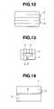
- FIG. 12is a plan view of an inductance device according to a third embodiment of the present invention.
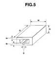
- the surface mount terminal 5 a according to the end of the wide width portion 41 and the surface mount terminal 5 b according to the end of the narrow width portion 42are fixed at the bottom face of the inductance device as shown in FIG. 11 .
- the inductance device according to this embodimentbecomes a surface mount component by providing these surface mount terminals 5 a , 5 b .
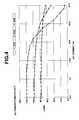
- the inductance valueis higher than that in the first embodiment, it is possible to prevent magnetic saturation from occurring similarly to the first embodiment, and DC characteristic thereof shows almost constant inductance value L in a high level range of DC current I. Moreover, it is possible to decrease variation of the inductance value of produced individual inductance devices
- a gap according to the slit 3is provided and their constructions allow the inductance value to be designed minute value not more than 1 ⁇ H. Also high current is acceptable to flow, so they are suitable for the inductance device of the step down type DC/DC converter circuit using for the power supply unit of computers as shown in FIG. 8 .
- it is easy to make as a surface mount componentbecause the shape of the ferrite core is polygonal tube-like, and it is possible to be small for its mount space because the dimensions of the ferrite core can be decreased, resulting in contributing to become smaller in size and thinner in thickness when it is adopted for notebook style personal computers.
Landscapes
- Engineering & Computer Science (AREA)
- Power Engineering (AREA)
- Microelectronics & Electronic Packaging (AREA)
- Coils Or Transformers For Communication (AREA)
- Coils Of Transformers For General Uses (AREA)
Abstract
Description
Claims (5)
Applications Claiming Priority (4)
| Application Number | Priority Date | Filing Date | Title |
|---|---|---|---|
| JP19216999 | 1999-06-03 | ||
| JP11-192169 | 1999-06-03 | ||
| JP11-268216 | 1999-09-22 | ||
| JP26821699AJP3366916B2 (en) | 1999-06-03 | 1999-09-22 | Inductance element |
Publications (1)
| Publication Number | Publication Date |
|---|---|
| US6356179B1true US6356179B1 (en) | 2002-03-12 |
Family
ID=26507155
Family Applications (1)
| Application Number | Title | Priority Date | Filing Date |
|---|---|---|---|
| US09/506,376Expired - LifetimeUS6356179B1 (en) | 1999-06-03 | 2000-02-18 | Inductance device |
Country Status (3)
| Country | Link |
|---|---|
| US (1) | US6356179B1 (en) |
| JP (1) | JP3366916B2 (en) |
| TW (1) | TW434594B (en) |
Cited By (39)
| Publication number | Priority date | Publication date | Assignee | Title |
|---|---|---|---|---|
| US6611187B2 (en)* | 2000-10-25 | 2003-08-26 | Nec Tokin Corporation | Magnetic core, coil assembly and power supply circuit using the same |
| US20040075516A1 (en)* | 2001-03-30 | 2004-04-22 | Nippon Chemi-Con Corporation | Inductance element and case |
| US20050012583A1 (en)* | 2003-07-16 | 2005-01-20 | Marvell World Trade, Ltd. | Power inductor with reduced DC current saturation |
| US20050012582A1 (en)* | 2003-07-16 | 2005-01-20 | Marvell International Ltd. | Power inductor with reduced DC current saturation |
| US20050012586A1 (en)* | 2003-07-16 | 2005-01-20 | Marvell World Trade Ltd. | Power inductor with reduced DC current saturation |
| US20050040800A1 (en)* | 2003-08-21 | 2005-02-24 | Sehat Sutardja | Digital low dropout regulator |
| US20050040796A1 (en)* | 2003-08-21 | 2005-02-24 | Marvell World Trade Ltd. | Voltage regulator |
| US20050212496A1 (en)* | 2004-03-26 | 2005-09-29 | Marvell World Trade Ltd. | Voltage regulator |
| US20060089022A1 (en)* | 2004-10-22 | 2006-04-27 | Sumida Corporation | Magnetic element |
| US20070176585A1 (en)* | 2004-07-13 | 2007-08-02 | Marvell World Trade Ltd. | Closed-loop digital control system for a DC/DC converter |
| US20080074225A1 (en)* | 2006-09-27 | 2008-03-27 | Hansen Thomas T | Inductor with thermally stable resistance |
| US20080122556A1 (en)* | 2004-12-28 | 2008-05-29 | Murata Manufacturing Co., Ltd. | Noise filter |
| US20080246577A1 (en)* | 2002-12-13 | 2008-10-09 | Volterra Semiconductor Corporation | Method For Making Magnetic Components With N-Phase Coupling, And Related Inductor Structures |
| US20080303624A1 (en)* | 2007-06-08 | 2008-12-11 | Nec Tokin Corporation | Inductor |
| US7525408B1 (en) | 2002-12-13 | 2009-04-28 | Volterra Semiconductor Corporation | Method for making magnetic components with N-phase coupling, and related inductor structures |
| US20090179723A1 (en)* | 2002-12-13 | 2009-07-16 | Volterra Semiconductor Corporation | Method For Making Magnetic Components With M-Phase Coupling, And Related Inductor Structures |
| US20090231081A1 (en)* | 2008-03-14 | 2009-09-17 | Alexandr Ikriannikov | Voltage Converter Inductor Having A Nonlinear Inductance Value |
| US20100102917A1 (en)* | 2004-09-08 | 2010-04-29 | Chun-Tiao Liu | Inductor |
| US20100182114A1 (en)* | 2009-01-16 | 2010-07-22 | Cyntec Co., Ltd. | Method for adjusting inductance of choke and method for designing choke |
| US20110018669A1 (en)* | 2009-07-22 | 2011-01-27 | Alexandr Ikriannikov | Low Profile Inductors For High Density Circuit Boards |
| US20110035607A1 (en)* | 2009-08-10 | 2011-02-10 | Alexandr Ikriannikov | Coupled Inductor With Improved Leakage Inductance Control |
| US20110032068A1 (en)* | 2009-08-10 | 2011-02-10 | Alexandr Ikriannikov | Coupled Inductor With Improved Leakage Inductance Control |
| US20110043317A1 (en)* | 2009-07-22 | 2011-02-24 | Alexandr Ikriannikov | Low Profile Inductors For High Density Circuit Boards |
| US7898379B1 (en)* | 2002-12-13 | 2011-03-01 | Volterra Semiconductor Corporation | Method for making magnetic components with N-phase coupling, and related inductor structures |
| US20110148560A1 (en)* | 2009-12-21 | 2011-06-23 | Alexandr Ikriannikov | Two-Phase Coupled Inductors Which Promote Improved Printed Circuit Board Layout |
| US20110169476A1 (en)* | 2010-01-14 | 2011-07-14 | Alexandr Ikriannikov | Asymmetrical Coupled Inductors And Associated Methods |
| US7994888B2 (en) | 2009-12-21 | 2011-08-09 | Volterra Semiconductor Corporation | Multi-turn inductors |
| US8299885B2 (en) | 2002-12-13 | 2012-10-30 | Volterra Semiconductor Corporation | Method for making magnetic components with M-phase coupling, and related inductor structures |
| US8638187B2 (en) | 2009-07-22 | 2014-01-28 | Volterra Semiconductor Corporation | Low profile inductors for high density circuit boards |
| US8674802B2 (en) | 2009-12-21 | 2014-03-18 | Volterra Semiconductor Corporation | Multi-turn inductors |
| US8975995B1 (en) | 2012-08-29 | 2015-03-10 | Volterra Semiconductor Corporation | Coupled inductors with leakage plates, and associated systems and methods |
| US9019063B2 (en) | 2009-08-10 | 2015-04-28 | Volterra Semiconductor Corporation | Coupled inductor with improved leakage inductance control |
| US9263177B1 (en) | 2012-03-19 | 2016-02-16 | Volterra Semiconductor LLC | Pin inductors and associated systems and methods |
| US9400294B2 (en) | 2009-09-04 | 2016-07-26 | Vishay Dale Electronics, Llc | Resistor with temperature coefficient of resistance (TCR) compensation |
| US9870856B2 (en) | 2013-03-15 | 2018-01-16 | Cooper Technologies Company | Magnetic component assembly with filled physical gap |
| CN108878096A (en)* | 2017-05-16 | 2018-11-23 | 台达电子企业管理(上海)有限公司 | Magnetic element |
| US20190051449A1 (en)* | 2015-09-22 | 2019-02-14 | Apple Inc. | Integrated magnetic passive devices using magnetic film |
| WO2021217448A1 (en)* | 2020-04-28 | 2021-11-04 | 深圳市铂科新材料股份有限公司 | Inductor and production process |
| US11555831B2 (en) | 2020-08-20 | 2023-01-17 | Vishay Dale Electronics, Llc | Resistors, current sense resistors, battery shunts, shunt resistors, and methods of making |
Families Citing this family (4)
| Publication number | Priority date | Publication date | Assignee | Title |
|---|---|---|---|---|
| JP4224039B2 (en)* | 2005-05-25 | 2009-02-12 | スミダコーポレーション株式会社 | Magnetic element |
| CN101071673B (en)* | 2006-02-15 | 2012-04-18 | 库帕技术公司 | Gapped core structure for magnetic elements |
| JP4885056B2 (en)* | 2007-05-22 | 2012-02-29 | スミダコーポレーション株式会社 | Magnetic element and method of manufacturing magnetic element |
| JP4999028B1 (en)* | 2011-10-26 | 2012-08-15 | 株式会社Maruwa | Impedance element |
Citations (5)
| Publication number | Priority date | Publication date | Assignee | Title |
|---|---|---|---|---|
| JPH02228008A (en)* | 1989-03-01 | 1990-09-11 | Toshiba Corp | Variable inductor |
| US5321373A (en)* | 1992-04-03 | 1994-06-14 | Digital Equipment Corporation | Combined differential-mode common-mode noise filter |
| US5783978A (en)* | 1995-06-21 | 1998-07-21 | Matsushita Electric Industrial Co., Ltd. | Band rejection filter having a plurality of dielectric resonator with cutout portions having electrodes therein |
| US5844462A (en)* | 1996-04-29 | 1998-12-01 | Alliedsignal Inc. | Magnetic core-coil assembly for spark ignition systems |
| US6144279A (en)* | 1997-03-18 | 2000-11-07 | Alliedsignal Inc. | Electrical choke for power factor correction |
- 1999
- 1999-09-22JPJP26821699Apatent/JP3366916B2/ennot_activeExpired - Lifetime
- 1999-12-31TWTW088123397Apatent/TW434594B/ennot_activeIP Right Cessation
- 2000
- 2000-02-18USUS09/506,376patent/US6356179B1/ennot_activeExpired - Lifetime
Patent Citations (5)
| Publication number | Priority date | Publication date | Assignee | Title |
|---|---|---|---|---|
| JPH02228008A (en)* | 1989-03-01 | 1990-09-11 | Toshiba Corp | Variable inductor |
| US5321373A (en)* | 1992-04-03 | 1994-06-14 | Digital Equipment Corporation | Combined differential-mode common-mode noise filter |
| US5783978A (en)* | 1995-06-21 | 1998-07-21 | Matsushita Electric Industrial Co., Ltd. | Band rejection filter having a plurality of dielectric resonator with cutout portions having electrodes therein |
| US5844462A (en)* | 1996-04-29 | 1998-12-01 | Alliedsignal Inc. | Magnetic core-coil assembly for spark ignition systems |
| US6144279A (en)* | 1997-03-18 | 2000-11-07 | Alliedsignal Inc. | Electrical choke for power factor correction |
Cited By (117)
| Publication number | Priority date | Publication date | Assignee | Title |
|---|---|---|---|---|
| US6611187B2 (en)* | 2000-10-25 | 2003-08-26 | Nec Tokin Corporation | Magnetic core, coil assembly and power supply circuit using the same |
| US20040075516A1 (en)* | 2001-03-30 | 2004-04-22 | Nippon Chemi-Con Corporation | Inductance element and case |
| US7362202B2 (en) | 2001-03-30 | 2008-04-22 | Nippon Chemi-Con Corporation | Inductance element and case |
| US7196605B2 (en)* | 2001-03-30 | 2007-03-27 | Nippon Chemi-Con Corporation | Inductance element and case |
| US20070040640A1 (en)* | 2001-03-30 | 2007-02-22 | Nippon Chemi-Con Corporation | Inductance element and case |
| US9147515B2 (en) | 2002-12-13 | 2015-09-29 | Volterra Semiconductor LLC | Method for making magnetic components with M-phase coupling, and related inductor structures |
| US7864016B1 (en) | 2002-12-13 | 2011-01-04 | Volterra Semiconductor Corporation | Method for making magnetic components with N-phase coupling, and related inductor structures |
| US7746209B1 (en) | 2002-12-13 | 2010-06-29 | Volterra Semiconductor Corporation | Method for making magnetic components with N-phase coupling, and related inductor structures |
| US8299885B2 (en) | 2002-12-13 | 2012-10-30 | Volterra Semiconductor Corporation | Method for making magnetic components with M-phase coupling, and related inductor structures |
| US8350658B1 (en) | 2002-12-13 | 2013-01-08 | Volterra Semiconductor Corporation | Method for making magnetic components with N-phase coupling, and related inductor structures |
| US8847722B2 (en) | 2002-12-13 | 2014-09-30 | Volterra Semiconductor Corporation | Method for making magnetic components with N-phase coupling, and related inductor structures |
| US8779885B2 (en) | 2002-12-13 | 2014-07-15 | Volterra Semiconductor Corporation | Method for making magnetic components with M-phase coupling, and related inductor structures |
| US20090179723A1 (en)* | 2002-12-13 | 2009-07-16 | Volterra Semiconductor Corporation | Method For Making Magnetic Components With M-Phase Coupling, And Related Inductor Structures |
| US7525408B1 (en) | 2002-12-13 | 2009-04-28 | Volterra Semiconductor Corporation | Method for making magnetic components with N-phase coupling, and related inductor structures |
| US7772955B1 (en) | 2002-12-13 | 2010-08-10 | Volterra Semiconductor Corporation | Method for making magnetic components with N-phase coupling, and related inductor structures |
| US7498920B2 (en)* | 2002-12-13 | 2009-03-03 | Volterra Semiconductor Corporation | Method for making magnetic components with N-phase coupling, and related inductor structures |
| US7893806B1 (en) | 2002-12-13 | 2011-02-22 | Volterra Semiconductor Corporation | Method for making magnetic components with N-phase coupling, and related inductor structures |
| US7965165B2 (en) | 2002-12-13 | 2011-06-21 | Volterra Semiconductor Corporation | Method for making magnetic components with M-phase coupling, and related inductor structures |
| US8786395B2 (en) | 2002-12-13 | 2014-07-22 | Volterra Semiconductor Corporation | Method for making magnetic components with M-phase coupling, and related inductor structures |
| US20080246577A1 (en)* | 2002-12-13 | 2008-10-09 | Volterra Semiconductor Corporation | Method For Making Magnetic Components With N-Phase Coupling, And Related Inductor Structures |
| US8836461B2 (en) | 2002-12-13 | 2014-09-16 | Volterra Semiconductor Corporation | Method for making magnetic components with M-phase coupling, and related inductor structures |
| US7898379B1 (en)* | 2002-12-13 | 2011-03-01 | Volterra Semiconductor Corporation | Method for making magnetic components with N-phase coupling, and related inductor structures |
| US9019064B2 (en) | 2002-12-13 | 2015-04-28 | Volterra Semiconductor Corporation | Method for making magnetic components with M-phase coupling, and related inductor structures |
| US20060158297A1 (en)* | 2003-07-16 | 2006-07-20 | Marvell World Trade Ltd. | Power inductor with reduced DC current saturation |
| US7868725B2 (en) | 2003-07-16 | 2011-01-11 | Marvell World Trade Ltd. | Power inductor with reduced DC current saturation |
| US20050012583A1 (en)* | 2003-07-16 | 2005-01-20 | Marvell World Trade, Ltd. | Power inductor with reduced DC current saturation |
| US20070171019A1 (en)* | 2003-07-16 | 2007-07-26 | Marvell World Trade Ltd. | Power inductor with reduced DC current saturation |
| US20070163110A1 (en)* | 2003-07-16 | 2007-07-19 | Marvell World Trade Ltd. | Power inductor with reduced DC current saturation |
| US7218197B2 (en) | 2003-07-16 | 2007-05-15 | Marvell World Trade Ltd. | Power inductor with reduced DC current saturation |
| US7489219B2 (en) | 2003-07-16 | 2009-02-10 | Marvell World Trade Ltd. | Power inductor with reduced DC current saturation |
| US20060158298A1 (en)* | 2003-07-16 | 2006-07-20 | Marvell World Trade Ltd. | Power inductor with reduced DC current saturation |
| US20060158299A1 (en)* | 2003-07-16 | 2006-07-20 | Marvell World Trade Ltd. | Power inductor with reduced DC current saturation |
| US20060114091A1 (en)* | 2003-07-16 | 2006-06-01 | Marvell World Trade, Ltd. | Power inductor with reduced DC current saturation |
| US20060114093A1 (en)* | 2003-07-16 | 2006-06-01 | Marvell World Trade, Ltd. | Power inductor with reduced DC current saturation |
| US20060082430A1 (en)* | 2003-07-16 | 2006-04-20 | Marvell International Ltd. | Power inductor with reduced DC current saturation |
| US20050012582A1 (en)* | 2003-07-16 | 2005-01-20 | Marvell International Ltd. | Power inductor with reduced DC current saturation |
| US7023313B2 (en)* | 2003-07-16 | 2006-04-04 | Marvell World Trade Ltd. | Power inductor with reduced DC current saturation |
| US20050012586A1 (en)* | 2003-07-16 | 2005-01-20 | Marvell World Trade Ltd. | Power inductor with reduced DC current saturation |
| US7987580B2 (en) | 2003-07-16 | 2011-08-02 | Marvell World Trade Ltd. | Method of fabricating conductor crossover structure for power inductor |
| US8028401B2 (en) | 2003-07-16 | 2011-10-04 | Marvell World Trade Ltd. | Method of fabricating a conducting crossover structure for a power inductor |
| US7882614B2 (en) | 2003-07-16 | 2011-02-08 | Marvell World Trade Ltd. | Method for providing a power inductor |
| US8035471B2 (en)* | 2003-07-16 | 2011-10-11 | Marvell World Trade Ltd. | Power inductor with reduced DC current saturation |
| US7307502B2 (en) | 2003-07-16 | 2007-12-11 | Marvell World Trade Ltd. | Power inductor with reduced DC current saturation |
| US8098123B2 (en) | 2003-07-16 | 2012-01-17 | Marvell World Trade Ltd. | Power inductor with reduced DC current saturation |
| US7849586B2 (en) | 2003-07-16 | 2010-12-14 | Marvell World Trade Ltd. | Method of making a power inductor with reduced DC current saturation |
| US20100277141A1 (en)* | 2003-08-21 | 2010-11-04 | Sehat Sutardja | Digital low dropout regulator |
| US20050040796A1 (en)* | 2003-08-21 | 2005-02-24 | Marvell World Trade Ltd. | Voltage regulator |
| US20050040800A1 (en)* | 2003-08-21 | 2005-02-24 | Sehat Sutardja | Digital low dropout regulator |
| US7760525B2 (en) | 2003-08-21 | 2010-07-20 | Marvell World Trade Ltd. | Voltage regulator |
| US7872454B2 (en) | 2003-08-21 | 2011-01-18 | Marvell World Trade Ltd. | Digital low dropout regulator |
| US8299763B2 (en) | 2003-08-21 | 2012-10-30 | Marvell World Trade Ltd. | Digital low dropout regulator |
| US20050212496A1 (en)* | 2004-03-26 | 2005-09-29 | Marvell World Trade Ltd. | Voltage regulator |
| US8324872B2 (en) | 2004-03-26 | 2012-12-04 | Marvell World Trade, Ltd. | Voltage regulator with coupled inductors having high coefficient of coupling |
| US20100171478A1 (en)* | 2004-07-13 | 2010-07-08 | Runsheng He | Closed-loop digital control system for a dc/dc converter |
| US8183846B2 (en) | 2004-07-13 | 2012-05-22 | Marvell World Trade Ltd. | Method and apparatus for controlling a DC/DC converter |
| US7679347B2 (en) | 2004-07-13 | 2010-03-16 | Marvell World Trade Ltd. | Closed-loop digital control system for a DC/DC converter |
| US20070176585A1 (en)* | 2004-07-13 | 2007-08-02 | Marvell World Trade Ltd. | Closed-loop digital control system for a DC/DC converter |
| US7915993B2 (en)* | 2004-09-08 | 2011-03-29 | Cyntec Co., Ltd. | Inductor |
| US20100102917A1 (en)* | 2004-09-08 | 2010-04-29 | Chun-Tiao Liu | Inductor |
| US20060089022A1 (en)* | 2004-10-22 | 2006-04-27 | Sumida Corporation | Magnetic element |
| US7280025B2 (en)* | 2004-10-22 | 2007-10-09 | Sumida Corporation | Magnetic element |
| US20080122556A1 (en)* | 2004-12-28 | 2008-05-29 | Murata Manufacturing Co., Ltd. | Noise filter |
| US7605677B2 (en) | 2004-12-28 | 2009-10-20 | Murata Manufacturing Co., Ltd. | Noise filter having filter components fitted into depressions in a base member |
| US20080074225A1 (en)* | 2006-09-27 | 2008-03-27 | Hansen Thomas T | Inductor with thermally stable resistance |
| US8018310B2 (en) | 2006-09-27 | 2011-09-13 | Vishay Dale Electronics, Inc. | Inductor with thermally stable resistance |
| EP2722858A3 (en)* | 2006-09-27 | 2014-07-23 | Vishay Dale Electronics, Inc. | Inductor with thermally stable resistance |
| EP2095380A1 (en)* | 2006-09-27 | 2009-09-02 | Vishay Dale Electronics, Inc. | Inductor with thermally stable resistance |
| US8378772B2 (en) | 2006-09-27 | 2013-02-19 | Vishay Dale Electronics, Inc. | Inductor with thermally stable resistance |
| US8975994B2 (en) | 2006-09-27 | 2015-03-10 | Vishay Dale Electronics, Inc. | Inductor with thermally stable resistance |
| US9502171B2 (en) | 2006-09-27 | 2016-11-22 | Vishay Dale Electronics, Llc | Inductor with thermally stable resistance |
| US7679482B2 (en)* | 2007-06-08 | 2010-03-16 | Nec Tokin Corporation | Inductor |
| US20080303624A1 (en)* | 2007-06-08 | 2008-12-11 | Nec Tokin Corporation | Inductor |
| US8294544B2 (en) | 2008-03-14 | 2012-10-23 | Volterra Semiconductor Corporation | Method for making magnetic components with M-phase coupling, and related inductor structures |
| US9627125B2 (en) | 2008-03-14 | 2017-04-18 | Volterra Semiconductor LLC | Voltage converter inductor having a nonlinear inductance value |
| US20090237197A1 (en)* | 2008-03-14 | 2009-09-24 | Alexandr Ikriannikov | Method For Making Magnetic Components With M-Phase Coupling, And Related Inductor Structures |
| US20090231081A1 (en)* | 2008-03-14 | 2009-09-17 | Alexandr Ikriannikov | Voltage Converter Inductor Having A Nonlinear Inductance Value |
| US8836463B2 (en) | 2008-03-14 | 2014-09-16 | Volterra Semiconductor Corporation | Voltage converter inductor having a nonlinear inductance value |
| US20100182114A1 (en)* | 2009-01-16 | 2010-07-22 | Cyntec Co., Ltd. | Method for adjusting inductance of choke and method for designing choke |
| US8299882B2 (en) | 2009-07-22 | 2012-10-30 | Volterra Semiconductor Corporation | Low profile inductors for high density circuit boards |
| US20110043317A1 (en)* | 2009-07-22 | 2011-02-24 | Alexandr Ikriannikov | Low Profile Inductors For High Density Circuit Boards |
| US8941459B2 (en) | 2009-07-22 | 2015-01-27 | Volterra Semiconductor LLC | Low profile inductors for high density circuit boards |
| US20110018669A1 (en)* | 2009-07-22 | 2011-01-27 | Alexandr Ikriannikov | Low Profile Inductors For High Density Circuit Boards |
| US8638187B2 (en) | 2009-07-22 | 2014-01-28 | Volterra Semiconductor Corporation | Low profile inductors for high density circuit boards |
| US8674798B2 (en) | 2009-07-22 | 2014-03-18 | Volterra Semiconductor Corporation | Low profile inductors for high density circuit boards |
| US8040212B2 (en) | 2009-07-22 | 2011-10-18 | Volterra Semiconductor Corporation | Low profile inductors for high density circuit boards |
| US20110032068A1 (en)* | 2009-08-10 | 2011-02-10 | Alexandr Ikriannikov | Coupled Inductor With Improved Leakage Inductance Control |
| US20110035607A1 (en)* | 2009-08-10 | 2011-02-10 | Alexandr Ikriannikov | Coupled Inductor With Improved Leakage Inductance Control |
| US8237530B2 (en) | 2009-08-10 | 2012-08-07 | Volterra Semiconductor Corporation | Coupled inductor with improved leakage inductance control |
| US9019063B2 (en) | 2009-08-10 | 2015-04-28 | Volterra Semiconductor Corporation | Coupled inductor with improved leakage inductance control |
| US8102233B2 (en) | 2009-08-10 | 2012-01-24 | Volterra Semiconductor Corporation | Coupled inductor with improved leakage inductance control |
| US9400294B2 (en) | 2009-09-04 | 2016-07-26 | Vishay Dale Electronics, Llc | Resistor with temperature coefficient of resistance (TCR) compensation |
| US12009127B2 (en) | 2009-09-04 | 2024-06-11 | Vishay Dale Electronics, Llc | Resistor with temperature coefficient of resistance (TCR) compensation |
| US11562838B2 (en) | 2009-09-04 | 2023-01-24 | Vishay Dale Electronics, Llc | Resistor with temperature coefficient of resistance (TCR) compensation |
| US10796826B2 (en) | 2009-09-04 | 2020-10-06 | Vishay Dale Electronics, Llc | Resistor with temperature coefficient of resistance (TCR) compensation |
| US10217550B2 (en) | 2009-09-04 | 2019-02-26 | Vishay Dale Electronics, Llc | Resistor with temperature coefficient of resistance (TCR) compensation |
| US9779860B2 (en) | 2009-09-04 | 2017-10-03 | Vishay Dale Electronics, Llc | Resistor with temperature coefficient of resistance (TCR) compensation |
| US20110148560A1 (en)* | 2009-12-21 | 2011-06-23 | Alexandr Ikriannikov | Two-Phase Coupled Inductors Which Promote Improved Printed Circuit Board Layout |
| US8362867B2 (en) | 2009-12-21 | 2013-01-29 | Volterra Semicanductor Corporation | Multi-turn inductors |
| US9281115B2 (en) | 2009-12-21 | 2016-03-08 | Volterra Semiconductor LLC | Multi-turn inductors |
| US8674802B2 (en) | 2009-12-21 | 2014-03-18 | Volterra Semiconductor Corporation | Multi-turn inductors |
| US7994888B2 (en) | 2009-12-21 | 2011-08-09 | Volterra Semiconductor Corporation | Multi-turn inductors |
| US8174348B2 (en) | 2009-12-21 | 2012-05-08 | Volterra Semiconductor Corporation | Two-phase coupled inductors which promote improved printed circuit board layout |
| US8890644B2 (en) | 2009-12-21 | 2014-11-18 | Volterra Semiconductor LLC | Two-phase coupled inductors which promote improved printed circuit board layout |
| US20110169476A1 (en)* | 2010-01-14 | 2011-07-14 | Alexandr Ikriannikov | Asymmetrical Coupled Inductors And Associated Methods |
| US8330567B2 (en) | 2010-01-14 | 2012-12-11 | Volterra Semiconductor Corporation | Asymmetrical coupled inductors and associated methods |
| US9263177B1 (en) | 2012-03-19 | 2016-02-16 | Volterra Semiconductor LLC | Pin inductors and associated systems and methods |
| US9721719B1 (en) | 2012-08-29 | 2017-08-01 | Volterra Semiconductor LLC | Coupled inductors with leakage plates, and associated systems and methods |
| US8975995B1 (en) | 2012-08-29 | 2015-03-10 | Volterra Semiconductor Corporation | Coupled inductors with leakage plates, and associated systems and methods |
| US11017939B2 (en) | 2013-03-15 | 2021-05-25 | Eaton Intelligent Power Limited | Magnetic component assembly with filled gap |
| US9870856B2 (en) | 2013-03-15 | 2018-01-16 | Cooper Technologies Company | Magnetic component assembly with filled physical gap |
| US20190051449A1 (en)* | 2015-09-22 | 2019-02-14 | Apple Inc. | Integrated magnetic passive devices using magnetic film |
| CN108878096A (en)* | 2017-05-16 | 2018-11-23 | 台达电子企业管理(上海)有限公司 | Magnetic element |
| US11056259B2 (en)* | 2017-05-16 | 2021-07-06 | Delta Electronics (Shanghai) Co., Ltd | Magnetic component |
| CN108878096B (en)* | 2017-05-16 | 2021-08-06 | 台达电子企业管理(上海)有限公司 | Magnetic element |
| WO2021217448A1 (en)* | 2020-04-28 | 2021-11-04 | 深圳市铂科新材料股份有限公司 | Inductor and production process |
| US11555831B2 (en) | 2020-08-20 | 2023-01-17 | Vishay Dale Electronics, Llc | Resistors, current sense resistors, battery shunts, shunt resistors, and methods of making |
| US12196783B2 (en) | 2020-08-20 | 2025-01-14 | Vishay Dale Electronics, Llc | Resistors, current sense resistors, battery shunts, shunt resistors, and methods of making |
Also Published As
| Publication number | Publication date |
|---|---|
| JP2001052934A (en) | 2001-02-23 |
| JP3366916B2 (en) | 2003-01-14 |
| TW434594B (en) | 2001-05-16 |
Similar Documents
| Publication | Publication Date | Title |
|---|---|---|
| US6356179B1 (en) | Inductance device | |
| US6342778B1 (en) | Low profile, surface mount magnetic devices | |
| JP4335887B2 (en) | Current detector | |
| US20080303624A1 (en) | Inductor | |
| US7397336B2 (en) | Coil component | |
| JP2000068132A (en) | Inverter transformer | |
| KR20030085099A (en) | Magnet with electromagnetic coil/impedance/sensor element | |
| US6326874B1 (en) | Terminal bobbin for a magnetic device and method of manufacture therefor | |
| US7295095B2 (en) | Electric component and method of producing the same | |
| JP2005064321A (en) | Coil parts and electronic devices equipped with the same | |
| JP2005227297A (en) | Magneto-impedance sensor element with electromagnet coil | |
| JP2020067401A (en) | Current detector and power module | |
| JP2007043527A (en) | Coil antenna | |
| JP3647133B2 (en) | Inductance element | |
| EP2320546B1 (en) | Dc/dc converter | |
| JP2006064535A (en) | Surge resistance measuring apparatus | |
| KR200187931Y1 (en) | Small-size transformer structure | |
| JPH0462807A (en) | Transformer | |
| JP3101641B2 (en) | Magnetic element | |
| JP2008192679A (en) | Three-phase common mode choke coil | |
| JP2007165623A (en) | Choke coil | |
| KR200267346Y1 (en) | A current detecting transformer for multi-use | |
| JPS6312970A (en) | Current detector | |
| JP2000331840A (en) | Coil parts | |
| JP4062079B2 (en) | Trance |
Legal Events
| Date | Code | Title | Description |
|---|---|---|---|
| AS | Assignment | Owner name:SUMIDA ELECTRIC CO., LTD., JAPAN Free format text:ASSIGNMENT OF ASSIGNORS INTEREST;ASSIGNOR:YAMADA, SATORU;REEL/FRAME:010574/0809 Effective date:19991007 | |
| AS | Assignment | Owner name:SUMIDA TECHNOLOGIES INCORPORATED, JAPAN Free format text:CHANGE OF NAME;ASSIGNOR:SUMIDA ELECTRIC CO., LTD.;REEL/FRAME:012433/0095 Effective date:20010914 Owner name:SUMIDA CORPORATION, JAPAN Free format text:CHANGE OF NAME;ASSIGNOR:SUMIDA ELECTRIC CO., LTD.;REEL/FRAME:012433/0095 Effective date:20010914 | |
| STCF | Information on status: patent grant | Free format text:PATENTED CASE | |
| FEPP | Fee payment procedure | Free format text:PAT HOLDER NO LONGER CLAIMS SMALL ENTITY STATUS, ENTITY STATUS SET TO UNDISCOUNTED (ORIGINAL EVENT CODE: STOL); ENTITY STATUS OF PATENT OWNER: LARGE ENTITY | |
| REFU | Refund | Free format text:REFUND - SURCHARGE, PETITION TO ACCEPT PYMT AFTER EXP, UNINTENTIONAL (ORIGINAL EVENT CODE: R2551); ENTITY STATUS OF PATENT OWNER: LARGE ENTITY | |
| AS | Assignment | Owner name:SUMIDA CORPORATION, JAPAN Free format text:ASSIGNMENT OF ASSIGNORS INTEREST;ASSIGNOR:SUMIDA ELECTRIC CO., LTD.;REEL/FRAME:016926/0811 Effective date:20050714 Owner name:SUMIDA ELECTRIC CO., LTD., JAPAN Free format text:MERGER;ASSIGNOR:SUMIDA TECHNOLOGIES INCORPORATED;REEL/FRAME:016926/0814 Effective date:20040202 | |
| FPAY | Fee payment | Year of fee payment:4 | |
| FPAY | Fee payment | Year of fee payment:8 | |
| FPAY | Fee payment | Year of fee payment:12 |