US6356168B1 - Sheet-metal filter - Google Patents
Sheet-metal filterDownload PDFInfo
- Publication number
- US6356168B1 US6356168B1US09/666,192US66619200AUS6356168B1US 6356168 B1US6356168 B1US 6356168B1US 66619200 AUS66619200 AUS 66619200AUS 6356168 B1US6356168 B1US 6356168B1
- Authority
- US
- United States
- Prior art keywords
- filter
- frame
- filter element
- resonant
- sheet
- Prior art date
- Legal status (The legal status is an assumption and is not a legal conclusion. Google has not performed a legal analysis and makes no representation as to the accuracy of the status listed.)
- Expired - Lifetime
Links
Images


Classifications
- H—ELECTRICITY
- H01—ELECTRIC ELEMENTS
- H01P—WAVEGUIDES; RESONATORS, LINES, OR OTHER DEVICES OF THE WAVEGUIDE TYPE
- H01P1/00—Auxiliary devices
- H01P1/20—Frequency-selective devices, e.g. filters
- H01P1/201—Filters for transverse electromagnetic waves
- H01P1/203—Strip line filters
- H01P1/20327—Electromagnetic interstage coupling
- H01P1/20354—Non-comb or non-interdigital filters
- H01P1/20381—Special shape resonators
- H—ELECTRICITY
- H01—ELECTRIC ELEMENTS
- H01P—WAVEGUIDES; RESONATORS, LINES, OR OTHER DEVICES OF THE WAVEGUIDE TYPE
- H01P11/00—Apparatus or processes specially adapted for manufacturing waveguides or resonators, lines, or other devices of the waveguide type
- H01P11/007—Manufacturing frequency-selective devices
Definitions
- This inventionrelates to high-frequency, e.g., microwave, filters.
- a filteris made from a single sheet of electrically conductive material, e.g., metal, preferably by stamping.
- the sheetis preferably all metal, e.g., a metal plate or a stacked assembly of metal sheets, but it may also be a metal-laminated non-conductive substrate, e.g., a printed-circuit board. In the latter case, the filter may advantageously be made by etching.
- An electromagnetically conductive housingpreferably encapsulates at least both faces of the sheet.
- the sheet of conductive materialdefines a frame, one or more resonator filter elements inside of the frame, and one or more supports attaching the resonators to the frame.
- At least one contact connected to the resonator filter elementprovides an electromagnetic contact thereto.
- the contactis a flange on at least one of the resonators, also defined by the sheet of conductive material.
- Another flange or the frame itselfserves as another contact to the filter.
- the flanged resonatoris rectangular and the flange and the supports extend from a side of the rectangle, whereby the distance between the flange and an end of the rectangular resonator that lies on the same side of the supports as the flange primarily determines the input characteristics of the filter.
- the resonant frequency of the filter elementis primarily determined by the length of the element ( ⁇ /2). Other factors, such as the width, the thickness, the tap point (L), and the resonators proximity to other metal also determine the resonant frequency.
- FIG. 1is a perspective view of a filter that includes a first illustrative embodiment of the invention
- FIG. 2shows illustrative dimensions of the resonant element of the filter of FIG. 1;
- FIG. 3is a graph of first operational characteristics of the resonant element of FIG. 2;
- FIG. 4is a graph of second operational characteristics of the resonant element of FIG. 2;
- FIG. 5is a perspective view of a filter that includes a second illustrative embodiment of the invention.
- FIG. 6is a perspective view of a filter that includes a third illustrative embodiment of the invention.
- FIG. 7is a perspective view of a filter that includes a fourth illustrative embodiment of the invention.
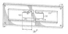
- FIG. 1shows a first bandpass filter 100 , which comprises an electrically conductive (e.g., metallic) filter layer 110 positioned inside a cavity formed by an electrically conductive housing 104 .
- the cavityis dimensioned to exhibit a waveguide cutoff frequency below the frequencies at which filter 100 is being used.
- Filter layer 110is a single sheet of electrically conductive material, such as a sheet of aluminum, steel, kovar, copper, or molybdenum. All these metals should be plated with copper, gold, or silver to enhance their conductivity and corrosion resistance.
- Filter layer 110also may be a metal-coated (laminated) insulating substrate, such as a printed-circuit board or plastic or ceramic.
- the printed-circuitmay be metal-coated on both sides, with one of the sides forming a part of housing 104 .
- filter layer 110is easily manufactured by stamping or etching.
- filter layer 110is easily manufactured by etching or plating, including edge plating. Cutting or other manufacturing methods may also be used.
- Filter layer 110need not be planar. Outer portions thereof may be bent substantially perpendicularly to the rest to form a part of the walls of housing 104 , or else are part of the interconnections between other filter layers or circuitry.
- Filter layer 110comprises a frame 112 , a resonator (resonant filter element) 114 inside of frame 112 , supports 116 connecting resonator 114 to frame 112 , and a coupler; a second, ground, contact is formed by frame 112 and supports 116 .
- the coupleris shown in FIG. 1 as a contact flange 118 located at the 50 ⁇ tap point and extending from resonator 114 , and acts as an inductive coupler.
- the couplercan also be an out-of-side coupler, or a capacitive coupler, or any other desired coupler.
- Flange 118forms a tap point between supports 116 and edges 122 of resonator 114 , so the closer flange 118 is to edge 122 , the more energy it couples in at a higher frequency.
- the inductive coupler formed by flange 118may extend from resonator 114 in the plane of filter element 110 ′ through a gap 270 in frame 112 , as shown in FIG. 5 .
- This planar filteris enclosed in a closure formed by an electrically conductive housing 104 , which behaves as a waveguide with a cut-off frequency lower than the second harmonic frequency of the filter center frequency.
- This planar configurationcomprising filter element 110 ′ as an input/output possesses up-down symmetry and nulls the coupling between the filter elements and the waveguide.
- flange 118may be bent away from the plane of filter layer 110 , as shown in FIG. 1, to extend outside of housing 104 through an opening 120 therein to form a connectorless coupling to, e.g., an antenna.
- the bent-up flange 118destroys the up-down symmetry of filter layer 110 ′ and hence destroys the suppression of the waveguide modes.
- the bent-up flange 118In order to regain the high suppression of the waveguide modes at the second harmonic position, the bent-up flange 118 must be positioned at an integer multiple of waveguide half-wavelength of the second harmonic frequency of the filter's center frequency from the inside edge of frame 112 . It renders the flange 118 in a null of the electromagnetic fields of the waveguide modes at the second harmonic frequency.
- both frame 112 and resonator 114are rectangular in shape.
- the important parametersare the loaded Q of the end resonators (which forms the input/output coupling to the filter) the center frequency of each resonator, and the interresonator coupling coefficients. They can be calculated for the specific type of filter that is desired. Electromagnetic (EM) simulations are used to relate these parameters to the specific structures and physical dimensions of the resonators for realization of the filter, because it is usually very difficult if not impossible to solve the problems analytically due to the complexity of the studied structures. The dimensions of an illustrative endcoupling resonator 114 are shown in FIG. 2 .
- the dimension “L” between the edge of flange 118 that is closest to support 116 and an end 122 of resonator 114 that lies on the same side of support 116 as flange 118is critical in that it is determinative of the input/output characteristics—the loaded Q and the center frequency f 0 of filter 100 and the loaded Q of the input and output resonators. It also de-tunes the center frequency f 0 of the input and output resonators from their natural, unloaded, half-wavelength resonance.
- the relationship of the loaded Q and center frequency ⁇ o to the parameter Lis determined by simulations, whose results are shown in FIG. 3 as curves 210 and 220 .
- FIG. 6shows a third filter 300 , which comprises an electrically conductive filter layer 310 mounted inside an electrically conductive housing 304 .
- Filter layer 310is also a single sheet of material, and comprises five resonators 311 - 315 to form a five-pole filter.
- Resonators 311 - 315are capacitively coupled to each other at their adjacent edges across gap G.
- Resonators 311 - 315are positioned inside a frame 312 and are connected thereto by supports 316 and 317 .
- Contact flanges 318 and 319extend from sides 320 of the two outermost resonators 310 and 314 .
- Filter layer 310is also easily manufactured by stamping or etching.
- Flange 318is bent away from the plane of filter element 310 and extends outside of housing 304 via orifice 322 to form a first contact to filter 300 .
- Flange 319extends outside of housing 304 through a gap 330 in frame 312 to form a second contact of filter 300 .
- Suppression of the low-frequency parasitic modeis achieved by designing the end resonators 311 and 314 properly such that the center frequency of the parasitic mode of the end resonators 311 and 314 are very different from that of the inner resonators 312 , 313 , and 315 .
- a desired frequency responsecan be achieved at any frequency.
- a filterwill often display some parasitic modes at the undesired places. They can be reduced or eliminated on a case-to-case basis by manipulating the structures in a way that suppresses those undesired modes but not the desired one by properly engineering the width and the shape of tabs 316 so that they do not perturb the desired modes of propagation in the resonant elements.
- FIG. 7shows a fourth filter 400 , which also comprises an electromagnetically conductive filter layer 410 mounted inside an electromagnetically conductive housing 404 .
- This designis particularity suited for implementing a transceiver duplexer.
- Filter layer 410defines dual side-by-side five-pole filters. Of course, any desired number of filters may be defined by a single filter layer 410 .
- the filtersmay be cascaded for better performance. Or, they may be used for different stages of a transmitter or a receiver. Or, one may be used for the transmitter and the other for the receiver of a wireless device.
- Filter layer 410is a single sheet of material and defines two frames 412 and 413 each holding five resonators 424 - 428 that are connected thereto by supports 416 .
- each of the filtersmay have a different number of resonators, of different dimensions, to achieve different filter characteristics.
- Contact flanges 419 and 418extend from sides 420 of the two outermost resonators 424 and 428 in each frame 412 and 413 and establish the input/output coupling to filter 400 . Alternately, this coupling can be obtained by coupling capacitively to the same elements 411 and 414 .
- Filter layer 410is likewise easily manufactured by stamping or etching. Flanges 418 and 419 are bent away from the plane of filter layer 410 and extend through orifice 422 outside of housing 404 to form a pair of contacts to each of the two filters.
- the resonatorsmay be twisted to lie at an angle to the plane of the filter frame, e.g., at 90° thereto.
- Such changes and modificationscan be made without departing from the spirit and the scope of the invention and without diminishing its attendant advantages. It is therefore intended that such changes and modifications be covered by the following claims except insofar as limited by the prior art.
Landscapes
- Physics & Mathematics (AREA)
- Electromagnetism (AREA)
- Engineering & Computer Science (AREA)
- Manufacturing & Machinery (AREA)
- Control Of Motors That Do Not Use Commutators (AREA)
Abstract
Description
Claims (12)
Priority Applications (1)
| Application Number | Priority Date | Filing Date | Title |
|---|---|---|---|
| US09/666,192US6356168B1 (en) | 2000-03-09 | 2000-09-21 | Sheet-metal filter |
Applications Claiming Priority (2)
| Application Number | Priority Date | Filing Date | Title |
|---|---|---|---|
| US52155600A | 2000-03-09 | 2000-03-09 | |
| US09/666,192US6356168B1 (en) | 2000-03-09 | 2000-09-21 | Sheet-metal filter |
Related Parent Applications (1)
| Application Number | Title | Priority Date | Filing Date |
|---|---|---|---|
| US52155600AContinuation-In-Part | 2000-03-09 | 2000-03-09 |
Publications (1)
| Publication Number | Publication Date |
|---|---|
| US6356168B1true US6356168B1 (en) | 2002-03-12 |
Family
ID=24077194
Family Applications (1)
| Application Number | Title | Priority Date | Filing Date |
|---|---|---|---|
| US09/666,192Expired - LifetimeUS6356168B1 (en) | 2000-03-09 | 2000-09-21 | Sheet-metal filter |
Country Status (4)
| Country | Link |
|---|---|
| US (1) | US6356168B1 (en) |
| EP (1) | EP1143552A1 (en) |
| JP (1) | JP2001308604A (en) |
| CA (1) | CA2332758A1 (en) |
Cited By (6)
| Publication number | Priority date | Publication date | Assignee | Title |
|---|---|---|---|---|
| US20100117765A1 (en)* | 2008-11-07 | 2010-05-13 | Commissariat A L'energie Atomique | Differential filtering device with coplanar coupled resonators and filtering antenna furnished with such a device |
| US20130107356A1 (en)* | 2011-10-26 | 2013-05-02 | Korea Maritime University Industry-Academic Cooperation Foundation | Terahertz band filter |
| US10320048B2 (en)* | 2017-08-17 | 2019-06-11 | Microelectronics Technology, Inc. | Circuit board and communication device with side coupler |
| CN113114382A (en)* | 2020-01-13 | 2021-07-13 | 华为技术有限公司 | Power supply filtering device |
| US12040523B2 (en) | 2019-04-04 | 2024-07-16 | Nokia Solutions And Networks Oy | Resonator and filter |
| US20240267029A1 (en)* | 2021-09-14 | 2024-08-08 | Telefonaktiebolaget Lm Ericsson (Publ) | Integrated low-pass and band-pass filter unit formed by sheet metal coated with dielectric material |
Families Citing this family (3)
| Publication number | Priority date | Publication date | Assignee | Title |
|---|---|---|---|---|
| TWI568203B (en)* | 2012-08-31 | 2017-01-21 | Yong-Sheng Huang | Harmonic Suppression Method of Radio Frequency Circuits |
| KR101939989B1 (en)* | 2018-08-01 | 2019-01-18 | 주식회사 엘트로닉스 | High frequency filter |
| CN113113743B (en)* | 2021-04-14 | 2022-06-10 | 立讯精密工业(滁州)有限公司 | Single-cavity resonator and radio frequency cavity filter |
Citations (9)
| Publication number | Priority date | Publication date | Assignee | Title |
|---|---|---|---|---|
| US2945195A (en)* | 1958-03-25 | 1960-07-12 | Thompson Ramo Wooldridge Inc | Microwave filter |
| US3104362A (en) | 1959-08-27 | 1963-09-17 | Thompson Ramo Wooldridge Inc | Microwave filter |
| US3806844A (en)* | 1972-10-27 | 1974-04-23 | Zenith Radio Corp | Uhf varactor tuner having a chassis of unitary construction |
| US4609892A (en)* | 1985-09-30 | 1986-09-02 | Motorola, Inc. | Stripline filter apparatus and method of making the same |
| US5225799A (en) | 1991-06-04 | 1993-07-06 | California Amplifier | Microwave filter fabrication method and filters therefrom |
| US5235298A (en)* | 1989-07-07 | 1993-08-10 | Ngk Spark Plug Co., Ltd. | Temperature compensated stripline filter for microwaves |
| US5352996A (en) | 1992-01-30 | 1994-10-04 | Leader Electronics Corp. | Interdigital bandpass filter |
| EP0766333A1 (en) | 1995-09-26 | 1997-04-02 | Solitra Oy | Coaxial resonator filter and method for manufacturing the same |
| US6005455A (en) | 1996-06-19 | 1999-12-21 | Telefonaktiebolaget Lm Ericsson | Integrated filter |
- 2000
- 2000-09-18EPEP00308083Apatent/EP1143552A1/ennot_activeWithdrawn
- 2000-09-21USUS09/666,192patent/US6356168B1/ennot_activeExpired - Lifetime
- 2001
- 2001-01-30CACA002332758Apatent/CA2332758A1/ennot_activeAbandoned
- 2001-03-09JPJP2001066153Apatent/JP2001308604A/enactivePending
Patent Citations (9)
| Publication number | Priority date | Publication date | Assignee | Title |
|---|---|---|---|---|
| US2945195A (en)* | 1958-03-25 | 1960-07-12 | Thompson Ramo Wooldridge Inc | Microwave filter |
| US3104362A (en) | 1959-08-27 | 1963-09-17 | Thompson Ramo Wooldridge Inc | Microwave filter |
| US3806844A (en)* | 1972-10-27 | 1974-04-23 | Zenith Radio Corp | Uhf varactor tuner having a chassis of unitary construction |
| US4609892A (en)* | 1985-09-30 | 1986-09-02 | Motorola, Inc. | Stripline filter apparatus and method of making the same |
| US5235298A (en)* | 1989-07-07 | 1993-08-10 | Ngk Spark Plug Co., Ltd. | Temperature compensated stripline filter for microwaves |
| US5225799A (en) | 1991-06-04 | 1993-07-06 | California Amplifier | Microwave filter fabrication method and filters therefrom |
| US5352996A (en) | 1992-01-30 | 1994-10-04 | Leader Electronics Corp. | Interdigital bandpass filter |
| EP0766333A1 (en) | 1995-09-26 | 1997-04-02 | Solitra Oy | Coaxial resonator filter and method for manufacturing the same |
| US6005455A (en) | 1996-06-19 | 1999-12-21 | Telefonaktiebolaget Lm Ericsson | Integrated filter |
Cited By (9)
| Publication number | Priority date | Publication date | Assignee | Title |
|---|---|---|---|---|
| US20100117765A1 (en)* | 2008-11-07 | 2010-05-13 | Commissariat A L'energie Atomique | Differential filtering device with coplanar coupled resonators and filtering antenna furnished with such a device |
| US8284001B2 (en)* | 2008-11-07 | 2012-10-09 | Commissariat à l'Energie Atomique | Differential filtering device with coplanar coupled resonators and filtering antenna furnished with such a device |
| US20130107356A1 (en)* | 2011-10-26 | 2013-05-02 | Korea Maritime University Industry-Academic Cooperation Foundation | Terahertz band filter |
| US8913315B2 (en)* | 2011-10-26 | 2014-12-16 | Korea Maritime University Industry-Academic Cooperation Foundation | Terahertz band filter |
| US10320048B2 (en)* | 2017-08-17 | 2019-06-11 | Microelectronics Technology, Inc. | Circuit board and communication device with side coupler |
| US12040523B2 (en) | 2019-04-04 | 2024-07-16 | Nokia Solutions And Networks Oy | Resonator and filter |
| CN113114382A (en)* | 2020-01-13 | 2021-07-13 | 华为技术有限公司 | Power supply filtering device |
| CN113114382B (en)* | 2020-01-13 | 2023-09-01 | 华为技术有限公司 | Power supply filtering device |
| US20240267029A1 (en)* | 2021-09-14 | 2024-08-08 | Telefonaktiebolaget Lm Ericsson (Publ) | Integrated low-pass and band-pass filter unit formed by sheet metal coated with dielectric material |
Also Published As
| Publication number | Publication date |
|---|---|
| EP1143552A1 (en) | 2001-10-10 |
| CA2332758A1 (en) | 2001-09-09 |
| JP2001308604A (en) | 2001-11-02 |
Similar Documents
| Publication | Publication Date | Title |
|---|---|---|
| US7746191B2 (en) | Waveguide to microstrip line transition having a conductive footprint for providing a contact free element | |
| EP1652270B1 (en) | Slotted cylinder antenna | |
| EP0948077B1 (en) | Dielectric resonator device | |
| US6373351B1 (en) | TM010 mode band elimination dielectric filter, dielectric duplexer and communication device using the same | |
| US20200403286A1 (en) | Dielectric cavity notch filter | |
| US10128552B2 (en) | Structure and electronic circuit | |
| WO2002058185A1 (en) | High frequency circuit element and high frequency circuit module | |
| US7323954B2 (en) | Dielectric ceramic filter with metal guide-can | |
| US6356168B1 (en) | Sheet-metal filter | |
| KR101812490B1 (en) | Designs and methods to implement surface mounting structures of SIW | |
| JP2005260570A (en) | Microstrip line waveguide converter | |
| FI113578B (en) | resonator | |
| CN114267958A (en) | A low-pass absorbing frequency selective structure with narrow transition band | |
| JPS638641B2 (en) | ||
| US20050140474A1 (en) | Dielectric resonator having a multilayer structure | |
| US20040246071A1 (en) | Radio-frequency filter, in particular in the form of a duplex filter | |
| CN111129757B (en) | Half-mode microstrip antenna and electronic equipment | |
| US7518472B2 (en) | Transmission line connecting structure and transmission/reception device | |
| CN211743415U (en) | Multifrequency Microstrip Antenna with Radiator Loaded Parasitic Resonator | |
| MXPA05006079A (en) | Finline type microwave band-pass filter. | |
| EP3598568B1 (en) | Tunable probe for high-performance cross-coupled rf filters | |
| JP3464820B2 (en) | Dielectric laminated resonator and dielectric filter | |
| JP4280160B2 (en) | Dielectric resonator, dielectric filter, and high-frequency module | |
| US6326867B1 (en) | Dielectric filter having resonators arranged in series | |
| JP4275512B2 (en) | Dielectric resonator, dielectric filter, and wireless communication device |
Legal Events
| Date | Code | Title | Description |
|---|---|---|---|
| AS | Assignment | Owner name:AVAYA TECHNOLOGY CORP., NEW JERSEY Free format text:ASSIGNMENT OF ASSIGNORS INTEREST;ASSIGNOR:LUCENT TECHNOLOGIES INC.;REEL/FRAME:012167/0778 Effective date:20000929 | |
| STCF | Information on status: patent grant | Free format text:PATENTED CASE | |
| AS | Assignment | Owner name:BANK OF NEW YORK, THE, NEW YORK Free format text:SECURITY INTEREST;ASSIGNOR:AVAYA TECHNOLOGY CORP.;REEL/FRAME:012762/0098 Effective date:20020405 | |
| FPAY | Fee payment | Year of fee payment:4 | |
| AS | Assignment | Owner name:CITIBANK, N.A., AS ADMINISTRATIVE AGENT, NEW YORK Free format text:SECURITY AGREEMENT;ASSIGNORS:AVAYA, INC.;AVAYA TECHNOLOGY LLC;OCTEL COMMUNICATIONS LLC;AND OTHERS;REEL/FRAME:020156/0149 Effective date:20071026 Owner name:CITIBANK, N.A., AS ADMINISTRATIVE AGENT,NEW YORK Free format text:SECURITY AGREEMENT;ASSIGNORS:AVAYA, INC.;AVAYA TECHNOLOGY LLC;OCTEL COMMUNICATIONS LLC;AND OTHERS;REEL/FRAME:020156/0149 Effective date:20071026 | |
| AS | Assignment | Owner name:CITICORP USA, INC., AS ADMINISTRATIVE AGENT, NEW Y Free format text:SECURITY AGREEMENT;ASSIGNORS:AVAYA, INC.;AVAYA TECHNOLOGY LLC;OCTEL COMMUNICATIONS LLC;AND OTHERS;REEL/FRAME:020166/0705 Effective date:20071026 Owner name:CITICORP USA, INC., AS ADMINISTRATIVE AGENT, NEW YORK Free format text:SECURITY AGREEMENT;ASSIGNORS:AVAYA, INC.;AVAYA TECHNOLOGY LLC;OCTEL COMMUNICATIONS LLC;AND OTHERS;REEL/FRAME:020166/0705 Effective date:20071026 Owner name:CITICORP USA, INC., AS ADMINISTRATIVE AGENT,NEW YO Free format text:SECURITY AGREEMENT;ASSIGNORS:AVAYA, INC.;AVAYA TECHNOLOGY LLC;OCTEL COMMUNICATIONS LLC;AND OTHERS;REEL/FRAME:020166/0705 Effective date:20071026 | |
| AS | Assignment | Owner name:AVAYA INC, NEW JERSEY Free format text:REASSIGNMENT;ASSIGNOR:AVAYA TECHNOLOGY LLC;REEL/FRAME:021158/0310 Effective date:20080625 | |
| AS | Assignment | Owner name:AVAYA TECHNOLOGY LLC, NEW JERSEY Free format text:CONVERSION FROM CORP TO LLC;ASSIGNOR:AVAYA TECHNOLOGY CORP.;REEL/FRAME:022071/0420 Effective date:20051004 | |
| FPAY | Fee payment | Year of fee payment:8 | |
| AS | Assignment | Owner name:BANK OF NEW YORK MELLON TRUST, NA, AS NOTES COLLATERAL AGENT, THE, PENNSYLVANIA Free format text:SECURITY AGREEMENT;ASSIGNOR:AVAYA INC., A DELAWARE CORPORATION;REEL/FRAME:025863/0535 Effective date:20110211 Owner name:BANK OF NEW YORK MELLON TRUST, NA, AS NOTES COLLAT Free format text:SECURITY AGREEMENT;ASSIGNOR:AVAYA INC., A DELAWARE CORPORATION;REEL/FRAME:025863/0535 Effective date:20110211 | |
| AS | Assignment | Owner name:BANK OF NEW YORK MELLON TRUST COMPANY, N.A., THE, PENNSYLVANIA Free format text:SECURITY AGREEMENT;ASSIGNOR:AVAYA, INC.;REEL/FRAME:030083/0639 Effective date:20130307 Owner name:BANK OF NEW YORK MELLON TRUST COMPANY, N.A., THE, Free format text:SECURITY AGREEMENT;ASSIGNOR:AVAYA, INC.;REEL/FRAME:030083/0639 Effective date:20130307 | |
| FPAY | Fee payment | Year of fee payment:12 | |
| AS | Assignment | Owner name:CITIBANK, N.A., AS ADMINISTRATIVE AGENT, NEW YORK Free format text:SECURITY INTEREST;ASSIGNORS:AVAYA INC.;AVAYA INTEGRATED CABINET SOLUTIONS INC.;OCTEL COMMUNICATIONS CORPORATION;AND OTHERS;REEL/FRAME:041576/0001 Effective date:20170124 | |
| AS | Assignment | Owner name:SILICON VALLEY BANK, CALIFORNIA Free format text:SECOND AMENDED AND RESTATED PATENT AND TRADEMARK SECURITY AGREEMENT;ASSIGNOR:EXTREME NETWORKS, INC.;REEL/FRAME:043200/0614 Effective date:20170714 | |
| AS | Assignment | Owner name:EXTREME NETWORKS, INC., CALIFORNIA Free format text:ASSIGNMENT OF ASSIGNORS INTEREST;ASSIGNORS:AVAYA INC.;AVAYA COMMUNICATION ISRAEL LTD;AVAYA HOLDINGS LIMITED;REEL/FRAME:043569/0047 Effective date:20170714 | |
| AS | Assignment | Owner name:SILICON VALLEY BANK, CALIFORNIA Free format text:THIRD AMENDED AND RESTATED PATENT AND TRADEMARK SECURITY AGREEMENT;ASSIGNOR:EXTREME NETWORKS, INC.;REEL/FRAME:044639/0300 Effective date:20171027 | |
| AS | Assignment | Owner name:OCTEL COMMUNICATIONS LLC (FORMERLY KNOWN AS OCTEL COMMUNICATIONS CORPORATION), CALIFORNIA Free format text:BANKRUPTCY COURT ORDER RELEASING ALL LIENS INCLUDING THE SECURITY INTEREST RECORDED AT REEL/FRAME 041576/0001;ASSIGNOR:CITIBANK, N.A.;REEL/FRAME:044893/0531 Effective date:20171128 Owner name:AVAYA INTEGRATED CABINET SOLUTIONS INC., CALIFORNIA Free format text:BANKRUPTCY COURT ORDER RELEASING ALL LIENS INCLUDING THE SECURITY INTEREST RECORDED AT REEL/FRAME 041576/0001;ASSIGNOR:CITIBANK, N.A.;REEL/FRAME:044893/0531 Effective date:20171128 Owner name:AVAYA INC., CALIFORNIA Free format text:BANKRUPTCY COURT ORDER RELEASING ALL LIENS INCLUDING THE SECURITY INTEREST RECORDED AT REEL/FRAME 025863/0535;ASSIGNOR:THE BANK OF NEW YORK MELLON TRUST, NA;REEL/FRAME:044892/0001 Effective date:20171128 Owner name:AVAYA INC. (FORMERLY KNOWN AS AVAYA TECHNOLOGY COR Free format text:BANKRUPTCY COURT ORDER RELEASING ALL LIENS INCLUDING THE SECURITY INTEREST RECORDED AT REEL/FRAME 012762/0098;ASSIGNOR:THE BANK OF NEW YORK;REEL/FRAME:044893/0001 Effective date:20171128 Owner name:VPNET TECHNOLOGIES, INC., CALIFORNIA Free format text:BANKRUPTCY COURT ORDER RELEASING ALL LIENS INCLUDING THE SECURITY INTEREST RECORDED AT REEL/FRAME 041576/0001;ASSIGNOR:CITIBANK, N.A.;REEL/FRAME:044893/0531 Effective date:20171128 Owner name:AVAYA INTEGRATED CABINET SOLUTIONS INC., CALIFORNI Free format text:BANKRUPTCY COURT ORDER RELEASING ALL LIENS INCLUDING THE SECURITY INTEREST RECORDED AT REEL/FRAME 041576/0001;ASSIGNOR:CITIBANK, N.A.;REEL/FRAME:044893/0531 Effective date:20171128 Owner name:AVAYA INC., CALIFORNIA Free format text:BANKRUPTCY COURT ORDER RELEASING ALL LIENS INCLUDING THE SECURITY INTEREST RECORDED AT REEL/FRAME 041576/0001;ASSIGNOR:CITIBANK, N.A.;REEL/FRAME:044893/0531 Effective date:20171128 Owner name:OCTEL COMMUNICATIONS LLC (FORMERLY KNOWN AS OCTEL Free format text:BANKRUPTCY COURT ORDER RELEASING ALL LIENS INCLUDING THE SECURITY INTEREST RECORDED AT REEL/FRAME 041576/0001;ASSIGNOR:CITIBANK, N.A.;REEL/FRAME:044893/0531 Effective date:20171128 Owner name:AVAYA INC., CALIFORNIA Free format text:BANKRUPTCY COURT ORDER RELEASING ALL LIENS INCLUDING THE SECURITY INTEREST RECORDED AT REEL/FRAME 030083/0639;ASSIGNOR:THE BANK OF NEW YORK MELLON TRUST COMPANY, N.A.;REEL/FRAME:045012/0666 Effective date:20171128 | |
| AS | Assignment | Owner name:AVAYA, INC., CALIFORNIA Free format text:RELEASE BY SECURED PARTY;ASSIGNOR:CITICORP USA, INC.;REEL/FRAME:045032/0213 Effective date:20171215 Owner name:OCTEL COMMUNICATIONS LLC, CALIFORNIA Free format text:RELEASE BY SECURED PARTY;ASSIGNOR:CITICORP USA, INC.;REEL/FRAME:045032/0213 Effective date:20171215 Owner name:SIERRA HOLDINGS CORP., NEW JERSEY Free format text:RELEASE BY SECURED PARTY;ASSIGNOR:CITICORP USA, INC.;REEL/FRAME:045032/0213 Effective date:20171215 Owner name:VPNET TECHNOLOGIES, INC., NEW JERSEY Free format text:RELEASE BY SECURED PARTY;ASSIGNOR:CITICORP USA, INC.;REEL/FRAME:045032/0213 Effective date:20171215 Owner name:AVAYA TECHNOLOGY, LLC, NEW JERSEY Free format text:RELEASE BY SECURED PARTY;ASSIGNOR:CITICORP USA, INC.;REEL/FRAME:045032/0213 Effective date:20171215 | |
| AS | Assignment | Owner name:BANK OF MONTREAL, NEW YORK Free format text:SECURITY INTEREST;ASSIGNOR:EXTREME NETWORKS, INC.;REEL/FRAME:046050/0546 Effective date:20180501 Owner name:EXTREME NETWORKS, INC., CALIFORNIA Free format text:RELEASE BY SECURED PARTY;ASSIGNOR:SILICON VALLEY BANK;REEL/FRAME:046051/0775 Effective date:20180501 |