US6354479B1 - Dissipative ceramic bonding tip - Google Patents
Dissipative ceramic bonding tipDownload PDFInfo
- Publication number
- US6354479B1 US6354479B1US09/514,454US51445400AUS6354479B1US 6354479 B1US6354479 B1US 6354479B1US 51445400 AUS51445400 AUS 51445400AUS 6354479 B1US6354479 B1US 6354479B1
- Authority
- US
- United States
- Prior art keywords
- dissipative
- bonding
- tip
- bonded
- forming
- Prior art date
- Legal status (The legal status is an assumption and is not a legal conclusion. Google has not performed a legal analysis and makes no representation as to the accuracy of the status listed.)
- Expired - Lifetime
Links
Images


Classifications
- B—PERFORMING OPERATIONS; TRANSPORTING
- B23—MACHINE TOOLS; METAL-WORKING NOT OTHERWISE PROVIDED FOR
- B23K—SOLDERING OR UNSOLDERING; WELDING; CLADDING OR PLATING BY SOLDERING OR WELDING; CUTTING BY APPLYING HEAT LOCALLY, e.g. FLAME CUTTING; WORKING BY LASER BEAM
- B23K20/00—Non-electric welding by applying impact or other pressure, with or without the application of heat, e.g. cladding or plating
- B23K20/002—Non-electric welding by applying impact or other pressure, with or without the application of heat, e.g. cladding or plating specially adapted for particular articles or work
- B23K20/004—Wire welding
- B23K20/005—Capillary welding
- B—PERFORMING OPERATIONS; TRANSPORTING
- B23—MACHINE TOOLS; METAL-WORKING NOT OTHERWISE PROVIDED FOR
- B23K—SOLDERING OR UNSOLDERING; WELDING; CLADDING OR PLATING BY SOLDERING OR WELDING; CUTTING BY APPLYING HEAT LOCALLY, e.g. FLAME CUTTING; WORKING BY LASER BEAM
- B23K20/00—Non-electric welding by applying impact or other pressure, with or without the application of heat, e.g. cladding or plating
- B23K20/02—Non-electric welding by applying impact or other pressure, with or without the application of heat, e.g. cladding or plating by means of a press ; Diffusion bonding
- B23K20/023—Thermo-compression bonding
- B23K20/025—Bonding tips therefor
- H—ELECTRICITY
- H01—ELECTRIC ELEMENTS
- H01L—SEMICONDUCTOR DEVICES NOT COVERED BY CLASS H10
- H01L24/00—Arrangements for connecting or disconnecting semiconductor or solid-state bodies; Methods or apparatus related thereto
- H01L24/74—Apparatus for manufacturing arrangements for connecting or disconnecting semiconductor or solid-state bodies
- H01L24/78—Apparatus for connecting with wire connectors
- H—ELECTRICITY
- H01—ELECTRIC ELEMENTS
- H01L—SEMICONDUCTOR DEVICES NOT COVERED BY CLASS H10
- H01L24/00—Arrangements for connecting or disconnecting semiconductor or solid-state bodies; Methods or apparatus related thereto
- H01L24/80—Methods for connecting semiconductor or other solid state bodies using means for bonding being attached to, or being formed on, the surface to be connected
- H01L24/85—Methods for connecting semiconductor or other solid state bodies using means for bonding being attached to, or being formed on, the surface to be connected using a wire connector
- H—ELECTRICITY
- H01—ELECTRIC ELEMENTS
- H01L—SEMICONDUCTOR DEVICES NOT COVERED BY CLASS H10
- H01L2224/00—Indexing scheme for arrangements for connecting or disconnecting semiconductor or solid-state bodies and methods related thereto as covered by H01L24/00
- H01L2224/01—Means for bonding being attached to, or being formed on, the surface to be connected, e.g. chip-to-package, die-attach, "first-level" interconnects; Manufacturing methods related thereto
- H01L2224/42—Wire connectors; Manufacturing methods related thereto
- H01L2224/44—Structure, shape, material or disposition of the wire connectors prior to the connecting process
- H01L2224/45—Structure, shape, material or disposition of the wire connectors prior to the connecting process of an individual wire connector
- H01L2224/45001—Core members of the connector
- H01L2224/45099—Material
- H01L2224/451—Material with a principal constituent of the material being a metal or a metalloid, e.g. boron (B), silicon (Si), germanium (Ge), arsenic (As), antimony (Sb), tellurium (Te) and polonium (Po), and alloys thereof
- H01L2224/45138—Material with a principal constituent of the material being a metal or a metalloid, e.g. boron (B), silicon (Si), germanium (Ge), arsenic (As), antimony (Sb), tellurium (Te) and polonium (Po), and alloys thereof the principal constituent melting at a temperature of greater than or equal to 950°C and less than 1550°C
- H01L2224/45144—Gold (Au) as principal constituent
- H—ELECTRICITY
- H01—ELECTRIC ELEMENTS
- H01L—SEMICONDUCTOR DEVICES NOT COVERED BY CLASS H10
- H01L2224/00—Indexing scheme for arrangements for connecting or disconnecting semiconductor or solid-state bodies and methods related thereto as covered by H01L24/00
- H01L2224/74—Apparatus for manufacturing arrangements for connecting or disconnecting semiconductor or solid-state bodies and for methods related thereto
- H01L2224/78—Apparatus for connecting with wire connectors
- H01L2224/7825—Means for applying energy, e.g. heating means
- H01L2224/783—Means for applying energy, e.g. heating means by means of pressure
- H01L2224/78301—Capillary
- H01L2224/78302—Shape
- H—ELECTRICITY
- H01—ELECTRIC ELEMENTS
- H01L—SEMICONDUCTOR DEVICES NOT COVERED BY CLASS H10
- H01L2224/00—Indexing scheme for arrangements for connecting or disconnecting semiconductor or solid-state bodies and methods related thereto as covered by H01L24/00
- H01L2224/80—Methods for connecting semiconductor or other solid state bodies using means for bonding being attached to, or being formed on, the surface to be connected
- H01L2224/85—Methods for connecting semiconductor or other solid state bodies using means for bonding being attached to, or being formed on, the surface to be connected using a wire connector
- H01L2224/852—Applying energy for connecting
- H01L2224/85201—Compression bonding
- H01L2224/85205—Ultrasonic bonding
- H—ELECTRICITY
- H01—ELECTRIC ELEMENTS
- H01L—SEMICONDUCTOR DEVICES NOT COVERED BY CLASS H10
- H01L24/00—Arrangements for connecting or disconnecting semiconductor or solid-state bodies; Methods or apparatus related thereto
- H01L24/01—Means for bonding being attached to, or being formed on, the surface to be connected, e.g. chip-to-package, die-attach, "first-level" interconnects; Manufacturing methods related thereto
- H01L24/42—Wire connectors; Manufacturing methods related thereto
- H01L24/44—Structure, shape, material or disposition of the wire connectors prior to the connecting process
- H01L24/45—Structure, shape, material or disposition of the wire connectors prior to the connecting process of an individual wire connector
- H—ELECTRICITY
- H01—ELECTRIC ELEMENTS
- H01L—SEMICONDUCTOR DEVICES NOT COVERED BY CLASS H10
- H01L2924/00—Indexing scheme for arrangements or methods for connecting or disconnecting semiconductor or solid-state bodies as covered by H01L24/00
- H01L2924/0001—Technical content checked by a classifier
- H01L2924/00014—Technical content checked by a classifier the subject-matter covered by the group, the symbol of which is combined with the symbol of this group, being disclosed without further technical details
- H—ELECTRICITY
- H01—ELECTRIC ELEMENTS
- H01L—SEMICONDUCTOR DEVICES NOT COVERED BY CLASS H10
- H01L2924/00—Indexing scheme for arrangements or methods for connecting or disconnecting semiconductor or solid-state bodies as covered by H01L24/00
- H01L2924/01—Chemical elements
- H01L2924/01005—Boron [B]
- H—ELECTRICITY
- H01—ELECTRIC ELEMENTS
- H01L—SEMICONDUCTOR DEVICES NOT COVERED BY CLASS H10
- H01L2924/00—Indexing scheme for arrangements or methods for connecting or disconnecting semiconductor or solid-state bodies as covered by H01L24/00
- H01L2924/01—Chemical elements
- H01L2924/01006—Carbon [C]
- H—ELECTRICITY
- H01—ELECTRIC ELEMENTS
- H01L—SEMICONDUCTOR DEVICES NOT COVERED BY CLASS H10
- H01L2924/00—Indexing scheme for arrangements or methods for connecting or disconnecting semiconductor or solid-state bodies as covered by H01L24/00
- H01L2924/01—Chemical elements
- H01L2924/01011—Sodium [Na]
- H—ELECTRICITY
- H01—ELECTRIC ELEMENTS
- H01L—SEMICONDUCTOR DEVICES NOT COVERED BY CLASS H10
- H01L2924/00—Indexing scheme for arrangements or methods for connecting or disconnecting semiconductor or solid-state bodies as covered by H01L24/00
- H01L2924/01—Chemical elements
- H01L2924/01013—Aluminum [Al]
- H—ELECTRICITY
- H01—ELECTRIC ELEMENTS
- H01L—SEMICONDUCTOR DEVICES NOT COVERED BY CLASS H10
- H01L2924/00—Indexing scheme for arrangements or methods for connecting or disconnecting semiconductor or solid-state bodies as covered by H01L24/00
- H01L2924/01—Chemical elements
- H01L2924/01014—Silicon [Si]
- H—ELECTRICITY
- H01—ELECTRIC ELEMENTS
- H01L—SEMICONDUCTOR DEVICES NOT COVERED BY CLASS H10
- H01L2924/00—Indexing scheme for arrangements or methods for connecting or disconnecting semiconductor or solid-state bodies as covered by H01L24/00
- H01L2924/01—Chemical elements
- H01L2924/01027—Cobalt [Co]
- H—ELECTRICITY
- H01—ELECTRIC ELEMENTS
- H01L—SEMICONDUCTOR DEVICES NOT COVERED BY CLASS H10
- H01L2924/00—Indexing scheme for arrangements or methods for connecting or disconnecting semiconductor or solid-state bodies as covered by H01L24/00
- H01L2924/01—Chemical elements
- H01L2924/01039—Yttrium [Y]
- H—ELECTRICITY
- H01—ELECTRIC ELEMENTS
- H01L—SEMICONDUCTOR DEVICES NOT COVERED BY CLASS H10
- H01L2924/00—Indexing scheme for arrangements or methods for connecting or disconnecting semiconductor or solid-state bodies as covered by H01L24/00
- H01L2924/01—Chemical elements
- H01L2924/0104—Zirconium [Zr]
- H—ELECTRICITY
- H01—ELECTRIC ELEMENTS
- H01L—SEMICONDUCTOR DEVICES NOT COVERED BY CLASS H10
- H01L2924/00—Indexing scheme for arrangements or methods for connecting or disconnecting semiconductor or solid-state bodies as covered by H01L24/00
- H01L2924/01—Chemical elements
- H01L2924/01074—Tungsten [W]
- H—ELECTRICITY
- H01—ELECTRIC ELEMENTS
- H01L—SEMICONDUCTOR DEVICES NOT COVERED BY CLASS H10
- H01L2924/00—Indexing scheme for arrangements or methods for connecting or disconnecting semiconductor or solid-state bodies as covered by H01L24/00
- H01L2924/01—Chemical elements
- H01L2924/01078—Platinum [Pt]
- H—ELECTRICITY
- H01—ELECTRIC ELEMENTS
- H01L—SEMICONDUCTOR DEVICES NOT COVERED BY CLASS H10
- H01L2924/00—Indexing scheme for arrangements or methods for connecting or disconnecting semiconductor or solid-state bodies as covered by H01L24/00
- H01L2924/01—Chemical elements
- H01L2924/01079—Gold [Au]
- H—ELECTRICITY
- H01—ELECTRIC ELEMENTS
- H01L—SEMICONDUCTOR DEVICES NOT COVERED BY CLASS H10
- H01L2924/00—Indexing scheme for arrangements or methods for connecting or disconnecting semiconductor or solid-state bodies as covered by H01L24/00
- H01L2924/01—Chemical elements
- H01L2924/01082—Lead [Pb]
- H—ELECTRICITY
- H01—ELECTRIC ELEMENTS
- H01L—SEMICONDUCTOR DEVICES NOT COVERED BY CLASS H10
- H01L2924/00—Indexing scheme for arrangements or methods for connecting or disconnecting semiconductor or solid-state bodies as covered by H01L24/00
- H01L2924/049—Nitrides composed of metals from groups of the periodic table
- H01L2924/0494—4th Group
- H01L2924/04941—TiN
- H—ELECTRICITY
- H01—ELECTRIC ELEMENTS
- H01L—SEMICONDUCTOR DEVICES NOT COVERED BY CLASS H10
- H01L2924/00—Indexing scheme for arrangements or methods for connecting or disconnecting semiconductor or solid-state bodies as covered by H01L24/00
- H01L2924/10—Details of semiconductor or other solid state devices to be connected
- H01L2924/11—Device type
- H01L2924/14—Integrated circuits
Definitions
- This inventionrelates to bonding tool tips and more particularly to dissipative ceramic bonding tips for bonding electrical connections.
- Integrated circuitsare typically attached to a lead frame, and individual leads are connected to individual bond pads on the integrated circuit with wire.
- the wireis fed through a tubular bonding tool tip having a bonding pad at the output end. These tips are called capillary tips.
- An electrical discharge at the bonding tool tip supplied by a separate EFO (electronic flame off) devicemelts a bit of the wire, forming a bonding ball.
- Other bonding toolsdo not have the center tube, but have a feed hole or other feature for feeding the wire along, as needed.
- Some bonding tipshave no such wire arrangement, as the wire is supplied, as in magnetic disk recording devices, where the wire is insulated and bonded to a magnetic head and then to a flexible wire circuit.
- the wireWhen the bonding tip is on the integrated circuit die side of the wire connection, the wire will have a ball formed on the end of the wire, as above, before reaching the next die bonding pad. The ball then makes intimate contact with the film formed on the die pad on the integrated circuit.
- the bonding tipis then moved from the integrated circuit die pad, with gold wire being fed out as the tool is moved, onto the bond pad on the lead frame, and then scrubbed laterally by an ultrasonic transducer. Pressure from the bonding tool tip and the transducer, and capillary action, ‘flows’ the wire onto the bonding pad where molecular bonds produce a reliable electrical and mechanical connection.
- Bonding tool tipsmust be sufficiently hard to prevent deformation under pressure, and mechanically durable so that many bonds can be made before replacement.
- Prior art bonding tool tipswere made of aluminum oxide, which is an insulator, but provides the wearability to form thousands of bonding connections. Bonding tool tips must also be electrically designed to produce a reliable electrical contact, yet prevent electrostatic discharge damage to the part being bonded.
- Certain prior art deviceshave a one or more volt emission when the tip makes bonding contact. This could present a problem, as a one volt static discharge could generate a 20 milliamp current to flow, which, in certain instances, could cause the integrated circuit to fail due to this unwanted current.
- U.S. Pat. No. 5,816,472 to Linndescribes a durable alumina bonding tool “without electrically conductive metallic binders.”
- U.S. Pat. No. 5,616,257 to Haradadescribes covering the bonding tool electrode with an insulating cap or covering “made of a ceramic material” to produce a large electrostatic discharge that creates bonding balls of stable diameter.
- U.S. Pat. No. 5,280,979 to Polidescribes a vacuum wafer-handling tool having a ceramic coating “made with a controlled conductivity” to prevent a large electrostatic discharge.
- a bonding tool tipfor bonding electrical connections to bonding pads on electrical devices.
- a bonding tool tipmust conduct electricity at a rate sufficient to prevent charge buildup, but not at so high a rate as to overload the device being bonded.
- the tipneeds to discharge to avoid a sudden surge of current that could damage the part being bonded.
- a resistance in the tip assembly itselfshould range from 10 5 to 10 12 ohms.
- the toolsmust also have specific mechanical properties to function satisfactorily. The high stiffness and high abrasion resistance requirements have limited the possible material to ceramics (electrical non-conductors) or metals, such as tungsten carbide (electrical conductor).
- bonding tool tips with the desired electrical conductioncan be made with three different configurations.
- the toolscan be made from a uniform extrinsic semiconducting material which has dopant atoms in the appropriate concentration and valence states to produce sufficient mobile charge carrier densities (unbound electrons or holes) which will result in electrical conduction in the desired range.
- a uniform extrinsic semiconducting materialwhich has dopant atoms in the appropriate concentration and valence states to produce sufficient mobile charge carrier densities (unbound electrons or holes) which will result in electrical conduction in the desired range.
- a uniform extrinsic semiconducting materialwhich has dopant atoms in the appropriate concentration and valence states to produce sufficient mobile charge carrier densities (unbound electrons or holes) which will result in electrical conduction in the desired range.
- polycrystalline silicon carbideuniformly doped with boron.
- the toolscan be made by forming a thin layer of a highly doped semiconductor on an insulating core.
- the coreprovides the mechanical stiffness and the semiconductor surface layer provides abrasion resistance and provides a charge carrier path from the tip to mount which will permit dissipation of electrostatic charge at an acceptable rate.
- a diamond tip wedgethat is ion implanted with boron.
- the toolscan be made by forming a lightly doped semiconductor layer on a conducting core.
- the conducting coreprovides the mechanical stiffness and the semiconductor layer provides abrasion resistance and provides a charge carrier path from the tip to conducting core, which is electrically connected to the mount.
- the doping levelis chosen to produce conductivity through the layer which will permit dissipation of electrostatic charge at an acceptable rate.
- cobalt bonded tungsten carbide coated with titanium nitride carbidefor example, cobalt bonded tungsten carbide coated with titanium nitride carbide.
- FIG. 1is a cross-sectional view vastly enlarged of a capillary bonding tool tip
- FIG. 2is a cross-sectional view, vastly enlarged, of a capillary-type construction of the operating end or tip of a bonding tool;
- FIG. 3is a cross-sectional view of a bottle-neck capillary bonding tool tip
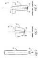
- FIG. 4is an isometric view of a wedge bonding tool tip
- FIGS. 5 a and 5 bare top and front views, respectively, of the wedge design bonding tool tip as shown in conjunction with FIG. 4;
- FIG. 6is an isometric view of a typical commercial apparatus utilized in the wire bonding of a semiconductor integrated circuit chip or other apparatus.
- FIG. 7a cross section of embodiments of FIG. 2 having two layers.
- FIG. 8a cross section of embodiments of FIG. 3 having two layers.
- FIG. 9a cross section of embodiments of FIG. 5 having two layers.
- FIG. 1illustrates a typical capillary bonding tool 10 .
- Such bonding toolsare usually about one-half inch (12-13 mm) long and about one-sixteenth inch (1.6 mm) in diameter.
- the bonding tool tip 12itself is usually from 3 to 10 mils (0.08 to 0.25 mm) long.
- Running the length of the tool itself, but not viewable in FIG. 1,is a tube hole which would accommodate a continuous fed length of gold wire (not shown).
- FIG. 2is a highly enlarged, cross-sectional view of the capillary bonding tool 10 as shown and described in FIG. 1 . Only that portion of the bonding tool 10 shown within the dotted circle in FIG. 1 is shown in FIG. 2 .
- Tool tip 12has the hole tube 14 which may run the entire length of bonding tool 10 .
- the exit hole 18is where the wire (not shown) would exit the tool tip 12 . If a ball is formed on the wire, the ball would be seen immediately adjacent the exit hole 18 .
- the chamfer 16 at the exit hole 18is there for at least two reasons. First, to accommodate a ball that has been formed at the end of the gold wire.
- the chamfer surface 16is provided to allow for smoother looping of the wire as the bonding tool 10 is moved from the bonding pad on an integrated circuit to the bonding pad (not shown) on a lead frame of an integrated circuit assembly.
- the wedge tool for disk drive bondingis used to capture the insulated wire, lay it on the head and ultrasonically bond it there.
- FIG. 3is an alternative embodiment of a bonding tool 10 showing similar features, as the hole tube 14 , chamfer surface 16 , and exit hole 18 .
- This bonding tool tipnamed a bottle-neck capillary tip, is provided for narrower bond situations where the bonding pitch (distance between the centers of the bonding pads) is smaller and smaller as the dimensions of an integrated circuit get smaller, or the number of circuits on a chip get larger, but the die area remains more or less constant.
- FIG. 4shows still another type of bonding tool 10 .
- This bonding toolis typically used with an integrated circuit die mounted on a lead frame (not shown). This is the case where the wires from the integrated circuit are not connected from the die to connections directly in an integrated circuit package, but from the integrated circuit die to a lead frame, which technology is well known to skilled practitioners in the art.
- the composition of the lead framebeing different than the composition of an integrated circuit package, the tip 12 of the bonding tool 10 must be different to accommodate the different physical attributes of the integrated circuit lead frame, as seen in FIGS. 5 a and 5 b.
- FIG. 6 aillustrates a typical wire bonding machine 60 for use in bonding wire leads in magnetic disk drive units. Shown within the dotted circle is the bonding tool 10 . The bonding tool 10 is mounted to arm 66 which is moved in the desired directions by the apparatus of wire bonding machine 60 . Such a machine is available as Model 7400 from the West Bond Company in Anaheim, Calif.
- Typical bonding tips available on the market todayare made of an insulator of alumina (Al 2 O 3 ), sometimes termed aluminum oxide. This is a very hard compound which has been used on commercial machines with success as it provides a reasonably long life in use as a wire bonding tool. To insure that it is an insulator no conductive binders are used in these bonding tips. However, as stated previously, the problem has existed that an electrostatic discharge from the bonding tool making contact with the bonding pad of the desired circuit can damage the very circuit it is wiring up.
- a bonding tool tipmust conduct electricity at a rate sufficient to prevent charge buildup, but not at so high a rate as to overload the device being bonded. It has been determined that the tool must have electrical conduction greater than one ten-billionth of a mho (i.e. >1 ⁇ 10 raised to the minus 12th power reciprocal ohms) but its electrical conductivity must be less than one one-hundred thousandth of a mho (i.e. ⁇ 1 ⁇ 10 raised to the minus fifth power reciprocal ohms).
- the resistanceshould be low enough so that the material is not an insulator, not allowing for any dissipation of charge and high enough so that it is not a conductor, allowing a current flow.
- a resistance in the tip assembly itselfshould range from 10 5 -10 12 ohms.
- 5 milliamps of currentwill damage them.
- no more than 2 to 3 milliamps of currentshould be allowed to pass through the tip to the head.
- the toolsmust also have specific mechanical properties to function satisfactorily.
- the high stiffness and high abrasion resistance requirementshave limited the possible material to ceramics (electrical non-conductors) or metal, such as tungsten carbide (electrical conductor).
- the tipshould have a Rockwell hardness of about 25 or above, preferably of about 32 or above. The tip needs to be able to last for at least two bondings.
- bonding tool tips with the desired electrical conductioncan be made with three different configurations.
- the toolscan be made from a uniform extrinsic semiconducting material which has dopant atoms in the appropriate concentration and valence states to produce sufficient mobile charge carrier densities (unbound electrons or holes) which will result in electrical conduction in the desired range.
- a uniform extrinsic semiconducting materialwhich has dopant atoms in the appropriate concentration and valence states to produce sufficient mobile charge carrier densities (unbound electrons or holes) which will result in electrical conduction in the desired range.
- a uniform extrinsic semiconducting materialwhich has dopant atoms in the appropriate concentration and valence states to produce sufficient mobile charge carrier densities (unbound electrons or holes) which will result in electrical conduction in the desired range.
- polycrystalline silicon carbideuniformly doped with boron.
- the toolscan be made by forming a thin layer of a highly doped semiconductor on an insulating core.
- the coreprovides the mechanical stiffness and the semiconductor surface layer provides abrasion resistance and provides a charge carrier path from the tip to the mount, which will permit dissipation of electrostatic charge at an acceptable rate.
- a diamond tip wedgethat has a surface that is ion implanted with boron or a doped ceramic.
- the toolscan be made by forming a lightly doped semiconductor layer on a conducting core.
- the conducting coreprovides the mechanical stiffness and the semiconductor layer provides abrasion resistance and provides a charge carrier path from the tip to conducting core, which is electrically connected to the mount.
- the doping levelis chosen to produce conductivity through the layer which will permit dissipation of electrostatic charge at an acceptable rate.
- cobalt bonded tungsten carbide coated with titanium nitride carbidefor example, cobalt bonded tungsten carbide coated with titanium nitride carbide.
- FIGS. 7, 8 and 9illustrate the two-layered structure of the last two configurations. This structure is not intended to be specific to the type of tool tip. Rather, it could be used for any bonding tool tip.
- the outer layersare labeled 71 , 81 and 91 and the cores are labeled 72 , 82 and 92 .
- layers 71 , 81 and 91are highly doped semiconductor and the cores 72 , 82 and 92 are insulators.
- layers 71 , 81 and 91are lightly doped semiconductor and the cores 72 , 82 and 92 are conductors. No significance should be attached to the relative thickness or scale of the portions of the layer 71 .
- Layer 71may or may not have a uniform thickness.
- Dissipative toolscan be manufactured by any of the following methods.
- the piecesmay then be treated to produce the desired surface layer by ion implementation, vapor deposition, chemical vapor deposition, physical deposition, electro-plating deposition, neutron bombardment, or combinations of the above.
- the piecesmay be subsequently heat treated in a controlled atmosphere to produce the desired layer properties through diffusion, recrystalization, dopant activation, or valence changes of metallic ions.
- Hot pressing reactive powdersFine particles of the desired composition are mixed with binders and sintering aids and then pressed in a mold at a high enough temperature to cause consolidation and binding of the individual particles into a solid structure with low porosity.
- the hot pressing atmosphereis chosen to control the valence of the dopant atoms.
- the piecesmay be machined to achieve the required tolerances.
- the piecesmay then be treated to produce the desired surface layer by ion implantation, vapor deposition, chemical vapor deposition, physical deposition, electo-plating deposition, neutron bombardment or combinations of the above.
- the piecesmay subsequently be heat treated in a controlled atmosphere to produce the desired layer properties through diffusion, recrystalization, dopant activation, or valence changes of metallic ions.
- the inventionfurther includes that the layer used in the bonding process could be the following composition of matter. More specifically, a formula for dissipated ceramic comprising alumina (aluminum oxide Al 2 O 3 ) and zirconia (zirconium oxide ZrO 2 ) and other elements. This mixture is both somewhat electrically conductive and mechanically durable.
- the tip of a bonding toolwill be coated with this material or it could be made completely out of this material The shape of the tip may be wedge or circular shaped as shown and described in the earlier FIGS. 1 to 5 .
- aluminacould extend from 15% to 85% and the range of zirconia from 15% to 85%
- another sampleincluded alumina at 40% and zirconia at 60%.
- the bonding tip of the present inventioncould be used for any number of different types of bonding. Two examples are ultrasonic and thermal bonding.
Landscapes
- Engineering & Computer Science (AREA)
- Computer Hardware Design (AREA)
- Microelectronics & Electronic Packaging (AREA)
- Power Engineering (AREA)
- Mechanical Engineering (AREA)
- Manufacturing & Machinery (AREA)
- Wire Bonding (AREA)
Abstract
Description
Claims (51)
Priority Applications (10)
| Application Number | Priority Date | Filing Date | Title |
|---|---|---|---|
| US09/514,454US6354479B1 (en) | 1999-02-25 | 2000-02-25 | Dissipative ceramic bonding tip |
| US10/036,579US6651864B2 (en) | 1999-02-25 | 2001-12-31 | Dissipative ceramic bonding tool tip |
| US10/650,169US6935548B2 (en) | 1999-02-25 | 2003-08-27 | Dissipative ceramic bonding tool tip |
| US10/943,151US7032802B2 (en) | 1999-02-25 | 2004-09-15 | Bonding tool with resistance |
| US10/942,311US7389905B2 (en) | 1999-02-25 | 2004-09-15 | Flip chip bonding tool tip |
| US11/107,308US7124927B2 (en) | 1999-02-25 | 2005-04-15 | Flip chip bonding tool and ball placement capillary |
| US11/227,982US20060071050A1 (en) | 1999-02-25 | 2005-09-14 | Multi-head tab bonding tool |
| US11/406,504US20060261132A1 (en) | 1999-02-25 | 2006-04-17 | Low range bonding tool |
| US11/582,826US20070131661A1 (en) | 1999-02-25 | 2006-10-17 | Solder ball placement system |
| US12/026,551US20080197172A1 (en) | 1999-02-25 | 2008-02-05 | Bonding Tool |
Applications Claiming Priority (2)
| Application Number | Priority Date | Filing Date | Title |
|---|---|---|---|
| US12169499P | 1999-02-25 | 1999-02-25 | |
| US09/514,454US6354479B1 (en) | 1999-02-25 | 2000-02-25 | Dissipative ceramic bonding tip |
Related Child Applications (2)
| Application Number | Title | Priority Date | Filing Date |
|---|---|---|---|
| US10/036,579Continuation-In-PartUS6651864B2 (en) | 1999-02-25 | 2001-12-31 | Dissipative ceramic bonding tool tip |
| US10/650,169Continuation-In-PartUS6935548B2 (en) | 1999-02-25 | 2003-08-27 | Dissipative ceramic bonding tool tip |
Publications (1)
| Publication Number | Publication Date |
|---|---|
| US6354479B1true US6354479B1 (en) | 2002-03-12 |
Family
ID=22398242
Family Applications (1)
| Application Number | Title | Priority Date | Filing Date |
|---|---|---|---|
| US09/514,454Expired - LifetimeUS6354479B1 (en) | 1999-02-25 | 2000-02-25 | Dissipative ceramic bonding tip |
Country Status (2)
| Country | Link |
|---|---|
| US (1) | US6354479B1 (en) |
| TW (1) | TW486400B (en) |
Cited By (28)
| Publication number | Priority date | Publication date | Assignee | Title |
|---|---|---|---|---|
| US20020158374A1 (en)* | 2001-02-28 | 2002-10-31 | Billiet Romain L. | Ultrasmall semiconductor bonding tools and method of fabrication thereof |
| WO2002087817A1 (en)* | 2001-05-01 | 2002-11-07 | Steven Frederick Reiber | Dissipative ceramic bonding tool tip |
| US20030015567A1 (en)* | 2001-07-17 | 2003-01-23 | Gil Perlberg | Ultra fine pitch capillary |
| US20040079927A1 (en)* | 2000-11-21 | 2004-04-29 | Saint-Gobain Ceramics & Plastics, Inc. | ESD dissipative ceramics |
| US20040094606A1 (en)* | 2001-07-17 | 2004-05-20 | Gil Perlberg | Capillary with contained inner chamfer |
| US20040242401A1 (en)* | 2003-05-30 | 2004-12-02 | Dou Yee Technologies Pte, Ltd. | Electro-static dissipative ceramic products and methods |
| US20050045692A1 (en)* | 2003-08-29 | 2005-03-03 | Fuaida Harun | Wirebonding insulated wire and capillary therefor |
| US20050109814A1 (en)* | 1999-02-25 | 2005-05-26 | Reiber Steven F. | Bonding tool with resistance |
| US20050109817A1 (en)* | 1999-02-25 | 2005-05-26 | Reiber Steven F. | Flip chip bonding tool tip |
| US20050121493A1 (en)* | 2003-12-04 | 2005-06-09 | Kulicke & Soffa Investments, Inc. | Multi-part capillary |
| US6905350B1 (en) | 2002-04-05 | 2005-06-14 | Maxtor Corporation | Two-step electrical connector and method using high resistance path for electrostatic discharge |
| US20050242155A1 (en)* | 1999-02-25 | 2005-11-03 | Reiber Steven F | Flip chip bonding tool and ball placement capillary |
| US20050254190A1 (en)* | 2003-03-19 | 2005-11-17 | Saint-Gobain Ceramics & Plastics, Inc. | ESD dissipative structural components |
| US20060071050A1 (en)* | 1999-02-25 | 2006-04-06 | Reiber Steven F | Multi-head tab bonding tool |
| US20060175584A1 (en)* | 2002-11-22 | 2006-08-10 | Saint-Gobain Ceramics & Plastics, Inc. | Zirconia toughened alumina ESD safe ceramic composition, component, and methods for making same |
| US20060261132A1 (en)* | 1999-02-25 | 2006-11-23 | Reiber Steven F | Low range bonding tool |
| US20060261133A1 (en)* | 2005-04-29 | 2006-11-23 | Eupec Europaische Gesellschaft Fur Leistungshalbleiter Mbh | Method and device for producing a bondable area region on a carrier |
| US20070085008A1 (en)* | 2005-10-13 | 2007-04-19 | Seagate Technology Llc | Ceramic corona discharge emitter tip |
| US20070085085A1 (en)* | 2005-08-08 | 2007-04-19 | Reiber Steven F | Dissipative pick and place tools for light wire and LED displays |
| US20070131661A1 (en)* | 1999-02-25 | 2007-06-14 | Reiber Steven F | Solder ball placement system |
| US20080197172A1 (en)* | 1999-02-25 | 2008-08-21 | Reiber Steven F | Bonding Tool |
| US20080216698A1 (en)* | 2007-03-06 | 2008-09-11 | Bio-Rad Laboratories, Inc. | Microdot printing head |
| US20080259236A1 (en)* | 2007-04-13 | 2008-10-23 | Saint-Gobain Ceramics & Plastics, Inc. | Electrostatic dissipative stage and effectors for use in forming lcd products |
| US20080257380A1 (en)* | 2007-04-16 | 2008-10-23 | Saint-Gobain Ceramics & Plastics, Inc. | Process of cleaning a substrate for microelectronic applications including directing mechanical energy through a fluid bath and apparatus of same |
| US20080299878A1 (en)* | 2007-06-04 | 2008-12-04 | Micron Technology, Inc. | Systems and methods for reducing electrostatic charge of semiconductor wafers |
| US9227188B2 (en) | 2013-04-11 | 2016-01-05 | Rarecyte, Inc. | Device, system, and method for selecting a target analyte or fluid |
| US20170209956A1 (en)* | 2016-01-26 | 2017-07-27 | Orthodyne Electronics Corporation | Wedge bonding tools, wedge bonding systems, and related methods |
| US10416046B2 (en) | 2013-04-11 | 2019-09-17 | Rarecyte, Inc. | Device, system, and method for selecting a target analyte |
Citations (44)
| Publication number | Priority date | Publication date | Assignee | Title |
|---|---|---|---|---|
| US2892924A (en) | 1959-06-30 | Electrode for melting and arc welding | ||
| US3538205A (en)* | 1966-10-14 | 1970-11-03 | Hughes Aircraft Co | Method of providing improved lossy dielectric structure for dissipating electrical microwave energy |
| US3660050A (en)* | 1969-06-23 | 1972-05-02 | Du Pont | Heterogeneous cobalt-bonded tungsten carbide |
| US3986653A (en)* | 1974-09-03 | 1976-10-19 | Tribotech | Method for coating bonding tools and product |
| US4020543A (en)* | 1975-06-26 | 1977-05-03 | Sola Basic Industries, Inc. | Two-piece capillary tip bonding tool |
| JPS5437114A (en)* | 1977-08-30 | 1979-03-19 | Mitsubishi Metal Corp | Highhstrength ceramic |
| US4171477A (en)* | 1976-03-16 | 1979-10-16 | International Business Machines Corporation | Micro-surface welding |
| US4182947A (en) | 1975-12-10 | 1980-01-08 | Brower Jerome S | Underwater cutting rod |
| US4315128A (en)* | 1978-04-07 | 1982-02-09 | Kulicke And Soffa Industries Inc. | Electrically heated bonding tool for the manufacture of semiconductor devices |
| US4331048A (en)* | 1979-06-08 | 1982-05-25 | Feldmuhle Aktiengesellschaft | Cutting tip for metal-removing processing |
| US4387283A (en) | 1981-08-03 | 1983-06-07 | Texas Instruments Incorporated | Apparatus and method of forming aluminum balls for ball bonding |
| US4390771A (en) | 1981-05-11 | 1983-06-28 | Fairchild Camera & Instrument Corp. | Bonding wire ball forming method and apparatus |
| US4502983A (en)* | 1983-06-28 | 1985-03-05 | Mamoru Omori | Composite silicon carbide sintered shapes and its manufacture |
| US4513190A (en)* | 1983-01-03 | 1985-04-23 | Small Precision Tools, Inc. | Protection of semiconductor wire bonding capillary from spark erosion |
| US4691854A (en)* | 1984-12-21 | 1987-09-08 | Texas Instruments Incorporated | Coatings for ceramic bonding capillaries |
| US4705204A (en) | 1985-03-01 | 1987-11-10 | Mitsubishi Denki Kabushiki Kaisha | Method of ball forming for wire bonding |
| JPS63164228A (en)* | 1986-12-25 | 1988-07-07 | Kyocera Corp | Ceramic wire bonding capillary |
| US4897710A (en)* | 1986-08-18 | 1990-01-30 | Sharp Kabushiki Kaisha | Semiconductor device |
| US4909427A (en)* | 1989-05-17 | 1990-03-20 | Plaisted Alan H | Bonding wire ball formation |
| US4998002A (en) | 1987-01-26 | 1991-03-05 | Hitachi, Ltd. | Wire-bonding method, wire-bonding apparatus, and semiconductor device produced by the wire-bonding method |
| EP0435423A2 (en)* | 1989-12-20 | 1991-07-03 | Sumitomo Electric Industries, Ltd. | A bonding tool |
| US5178742A (en) | 1990-03-08 | 1993-01-12 | Forschungszentrum Julich Gmbh | Method of and apparatus for forming a micromelt structure on an electrically-conductive probe tip |
| US5180093A (en)* | 1991-09-05 | 1993-01-19 | Cray Research, Inc. | Apparatus for ultrasonic bonding |
| US5214259A (en) | 1991-05-24 | 1993-05-25 | Kabushiki Kaisha Shinkawa | Method and apparatus for forming a ball at a bonding wire end |
| US5217154A (en)* | 1989-06-13 | 1993-06-08 | Small Precision Tools, Inc. | Semiconductor bonding tool |
| US5280979A (en)* | 1991-06-20 | 1994-01-25 | Recif, S.A. | Tip for a vacuum pipette with improved electrostatic discharge properties |
| US5290507A (en)* | 1991-02-19 | 1994-03-01 | Runkle Joseph C | Method for making tool steel with high thermal fatigue resistance |
| US5367956A (en)* | 1992-02-07 | 1994-11-29 | Fogle, Jr.; Homer W. | Hermetically-sealed electrically-absorptive low-pass radio frequency filters and electro-magnetically lossy ceramic materials for said filters |
| GB2287897A (en)* | 1994-03-31 | 1995-10-04 | Sumitomo Electric Industries | A high strength bonding tool and a process for producing the same |
| US5463197A (en) | 1993-06-30 | 1995-10-31 | Mitsubishi Denki Kabushiki Kaisha | Apparatus and method for forming wire bonding ball |
| US5463896A (en) | 1993-09-29 | 1995-11-07 | The United States Of America As Represented By The Secretary Of The Army | Stress tester |
| US5491605A (en) | 1994-12-23 | 1996-02-13 | International Business Machines Corporation | Shorted magnetoresistive head elements for electrical overstress and electrostatic discharge protection |
| US5527441A (en) | 1994-05-04 | 1996-06-18 | General Electric Company | Welding electrode with flat blade |
| US5544804A (en)* | 1994-06-08 | 1996-08-13 | Texas Instruments Incorporated | Capillary designs and process for fine pitch ball bonding |
| US5601740A (en) | 1993-11-16 | 1997-02-11 | Formfactor, Inc. | Method and apparatus for wirebonding, for severing bond wires, and for forming balls on the ends of bond wires |
| US5616257A (en) | 1994-03-18 | 1997-04-01 | Kabushiki Kaisha Shinkawa | Wire bonding method and apparatus |
| US5651901A (en) | 1993-10-15 | 1997-07-29 | Mitsubishi Denki Kabushiki Kaisha | Method and apparatus for surface treatment by electrical discharge machining |
| US5676856A (en) | 1994-04-25 | 1997-10-14 | Matsushita Electric Industrial Co., Ltd. | Electric discharge apparatus for cleaning electrode on workpiece and method thereof |
| US5797388A (en) | 1995-11-24 | 1998-08-25 | Kabushiki Kaisha Shinkawa | Wire-bonding apparatus and method using a covered wire |
| US5816472A (en)* | 1994-01-28 | 1998-10-06 | Hewlett-Packard Company | Bonding tool for tape automated assembly |
| US5827470A (en)* | 1996-11-13 | 1998-10-27 | Eastman Kodak Company | Method for preparing a zirconia/zirconium diboride composite |
| US5931368A (en)* | 1997-03-28 | 1999-08-03 | Kulicke And Soffa Investments, Inc | Long life bonding tool |
| US6030472A (en)* | 1997-12-04 | 2000-02-29 | Philip Morris Incorporated | Method of manufacturing aluminide sheet by thermomechanical processing of aluminide powders |
| US6073827A (en)* | 1998-08-27 | 2000-06-13 | Kulicke & Soffa Investments, Inc. | Wire bonding capillary with a conical surface |
- 2000
- 2000-02-25USUS09/514,454patent/US6354479B1/ennot_activeExpired - Lifetime
- 2000-10-13TWTW089120518Apatent/TW486400B/ennot_activeIP Right Cessation
Patent Citations (46)
| Publication number | Priority date | Publication date | Assignee | Title |
|---|---|---|---|---|
| US2892924A (en) | 1959-06-30 | Electrode for melting and arc welding | ||
| US3538205A (en)* | 1966-10-14 | 1970-11-03 | Hughes Aircraft Co | Method of providing improved lossy dielectric structure for dissipating electrical microwave energy |
| US3660050A (en)* | 1969-06-23 | 1972-05-02 | Du Pont | Heterogeneous cobalt-bonded tungsten carbide |
| US3986653A (en)* | 1974-09-03 | 1976-10-19 | Tribotech | Method for coating bonding tools and product |
| US4020543A (en)* | 1975-06-26 | 1977-05-03 | Sola Basic Industries, Inc. | Two-piece capillary tip bonding tool |
| US4182947A (en) | 1975-12-10 | 1980-01-08 | Brower Jerome S | Underwater cutting rod |
| US4171477A (en)* | 1976-03-16 | 1979-10-16 | International Business Machines Corporation | Micro-surface welding |
| JPS5437114A (en)* | 1977-08-30 | 1979-03-19 | Mitsubishi Metal Corp | Highhstrength ceramic |
| US4315128A (en)* | 1978-04-07 | 1982-02-09 | Kulicke And Soffa Industries Inc. | Electrically heated bonding tool for the manufacture of semiconductor devices |
| US4331048A (en)* | 1979-06-08 | 1982-05-25 | Feldmuhle Aktiengesellschaft | Cutting tip for metal-removing processing |
| US4390771A (en) | 1981-05-11 | 1983-06-28 | Fairchild Camera & Instrument Corp. | Bonding wire ball forming method and apparatus |
| US4387283A (en) | 1981-08-03 | 1983-06-07 | Texas Instruments Incorporated | Apparatus and method of forming aluminum balls for ball bonding |
| US4513190A (en)* | 1983-01-03 | 1985-04-23 | Small Precision Tools, Inc. | Protection of semiconductor wire bonding capillary from spark erosion |
| US4502983A (en)* | 1983-06-28 | 1985-03-05 | Mamoru Omori | Composite silicon carbide sintered shapes and its manufacture |
| US4691854A (en)* | 1984-12-21 | 1987-09-08 | Texas Instruments Incorporated | Coatings for ceramic bonding capillaries |
| US4705204A (en) | 1985-03-01 | 1987-11-10 | Mitsubishi Denki Kabushiki Kaisha | Method of ball forming for wire bonding |
| US4897710A (en)* | 1986-08-18 | 1990-01-30 | Sharp Kabushiki Kaisha | Semiconductor device |
| JPS63164228A (en)* | 1986-12-25 | 1988-07-07 | Kyocera Corp | Ceramic wire bonding capillary |
| US4998002A (en) | 1987-01-26 | 1991-03-05 | Hitachi, Ltd. | Wire-bonding method, wire-bonding apparatus, and semiconductor device produced by the wire-bonding method |
| US4909427A (en)* | 1989-05-17 | 1990-03-20 | Plaisted Alan H | Bonding wire ball formation |
| US5217154A (en)* | 1989-06-13 | 1993-06-08 | Small Precision Tools, Inc. | Semiconductor bonding tool |
| EP0435423A2 (en)* | 1989-12-20 | 1991-07-03 | Sumitomo Electric Industries, Ltd. | A bonding tool |
| US5178742A (en) | 1990-03-08 | 1993-01-12 | Forschungszentrum Julich Gmbh | Method of and apparatus for forming a micromelt structure on an electrically-conductive probe tip |
| US5290507A (en)* | 1991-02-19 | 1994-03-01 | Runkle Joseph C | Method for making tool steel with high thermal fatigue resistance |
| US5214259A (en) | 1991-05-24 | 1993-05-25 | Kabushiki Kaisha Shinkawa | Method and apparatus for forming a ball at a bonding wire end |
| US5280979A (en)* | 1991-06-20 | 1994-01-25 | Recif, S.A. | Tip for a vacuum pipette with improved electrostatic discharge properties |
| US5180093A (en)* | 1991-09-05 | 1993-01-19 | Cray Research, Inc. | Apparatus for ultrasonic bonding |
| US5367956A (en)* | 1992-02-07 | 1994-11-29 | Fogle, Jr.; Homer W. | Hermetically-sealed electrically-absorptive low-pass radio frequency filters and electro-magnetically lossy ceramic materials for said filters |
| US5463197A (en) | 1993-06-30 | 1995-10-31 | Mitsubishi Denki Kabushiki Kaisha | Apparatus and method for forming wire bonding ball |
| US5463896A (en) | 1993-09-29 | 1995-11-07 | The United States Of America As Represented By The Secretary Of The Army | Stress tester |
| US5651901A (en) | 1993-10-15 | 1997-07-29 | Mitsubishi Denki Kabushiki Kaisha | Method and apparatus for surface treatment by electrical discharge machining |
| US5601740A (en) | 1993-11-16 | 1997-02-11 | Formfactor, Inc. | Method and apparatus for wirebonding, for severing bond wires, and for forming balls on the ends of bond wires |
| US5816472A (en)* | 1994-01-28 | 1998-10-06 | Hewlett-Packard Company | Bonding tool for tape automated assembly |
| US5616257A (en) | 1994-03-18 | 1997-04-01 | Kabushiki Kaisha Shinkawa | Wire bonding method and apparatus |
| GB2287897A (en)* | 1994-03-31 | 1995-10-04 | Sumitomo Electric Industries | A high strength bonding tool and a process for producing the same |
| US5676856A (en) | 1994-04-25 | 1997-10-14 | Matsushita Electric Industrial Co., Ltd. | Electric discharge apparatus for cleaning electrode on workpiece and method thereof |
| US5527441A (en) | 1994-05-04 | 1996-06-18 | General Electric Company | Welding electrode with flat blade |
| US5649355A (en) | 1994-05-04 | 1997-07-22 | General Electric Company | Welding electrode with flat blade and related method of manufacture |
| US5544804A (en)* | 1994-06-08 | 1996-08-13 | Texas Instruments Incorporated | Capillary designs and process for fine pitch ball bonding |
| US5491605A (en) | 1994-12-23 | 1996-02-13 | International Business Machines Corporation | Shorted magnetoresistive head elements for electrical overstress and electrostatic discharge protection |
| US5797388A (en) | 1995-11-24 | 1998-08-25 | Kabushiki Kaisha Shinkawa | Wire-bonding apparatus and method using a covered wire |
| US5827470A (en)* | 1996-11-13 | 1998-10-27 | Eastman Kodak Company | Method for preparing a zirconia/zirconium diboride composite |
| US5827470B1 (en)* | 1996-11-13 | 1999-12-07 | Eastman Kodak Co | Method for preparing a zirconia/zirconium diboride composite |
| US5931368A (en)* | 1997-03-28 | 1999-08-03 | Kulicke And Soffa Investments, Inc | Long life bonding tool |
| US6030472A (en)* | 1997-12-04 | 2000-02-29 | Philip Morris Incorporated | Method of manufacturing aluminide sheet by thermomechanical processing of aluminide powders |
| US6073827A (en)* | 1998-08-27 | 2000-06-13 | Kulicke & Soffa Investments, Inc. | Wire bonding capillary with a conical surface |
Non-Patent Citations (8)
| Title |
|---|
| "Low-Current /High-Resistance Meters," Keithley Instruments Model 6517A Electrometer/High Resistance Meter, www.keithley.com, Keithley Instruments, Inc., This or an equivalent was in use for testing the Applicants' invention earlier than Feb. 25, 1999, pp. 112-115. |
| Carl E. Newberg, "Test Report," Anza Technology, Incorporated Static Dissipative Ceramic Rods for Wire Bonding Applications, Tested for Electrical Properties Discharge Current Resistance and Decay Time, Report #: 2000-92, River's Edge Technical Service, Nov. 29, 2000, pp. 1-5. |
| Instrument FAQs, Drivers, Libraries and Examples, Keithley Instruments Model 6517/6517A, http://208.240.90.52/techsupport/instruments/kth6517a.html, Keithley Instruments, Inc., 1999, pp. 1-2. |
| James R. Huntsman and Donald M. Yenni, Jr., "Test Methods for Static Control Products," Electrical Overstress/Electrostatic Discharge Symposium Proceedings, Sep. 21, 1982, pp. 94-109, vol. 4, IIT Research Institute, Chicago, IL. |
| Keithley Instruments Model 6517A Electometer/High Resistance Meter, http://208.240.90.52/products/prod_pages . . . K13_pages/summary_pgs/6517A_Summary.html, Keithley Instruments, Inc., This or an equivalent was in use for testing the Applicants' invention, earlier than Feb. 25, 1999, pp. 1-9. |
| Keytech 200 XV-2 ESD Simulator, http://www.kandus.com/Configurations/KEYTECH16842.html, K & Us Equipment, p. 1. |
| Newburg, Carl E., "Test Report", Anza Technolgy, Incorporated Static Dissipative Ceramic Rods for Wire Bonding Applications, Report 190 :2000-92, River's Edge Technical Service, Nov. 29, 2000, pp. 1-5.* |
| Stan Weitz, "Trends in ESD Test Methods," Materials Testing Section of the ETS Testing Laboratory, Electrotech Systems, http://www.electrotechsystems.com, the website has a copyright of 1998, pp. 1-7. |
Cited By (59)
| Publication number | Priority date | Publication date | Assignee | Title |
|---|---|---|---|---|
| US20060261132A1 (en)* | 1999-02-25 | 2006-11-23 | Reiber Steven F | Low range bonding tool |
| US20050109817A1 (en)* | 1999-02-25 | 2005-05-26 | Reiber Steven F. | Flip chip bonding tool tip |
| US7032802B2 (en)* | 1999-02-25 | 2006-04-25 | Reiber Steven F | Bonding tool with resistance |
| US6651864B2 (en)* | 1999-02-25 | 2003-11-25 | Steven Frederick Reiber | Dissipative ceramic bonding tool tip |
| US20040046007A1 (en)* | 1999-02-25 | 2004-03-11 | Steven-Frederick Reiber | Dissipative ceramic bonding tool tip |
| US20060071050A1 (en)* | 1999-02-25 | 2006-04-06 | Reiber Steven F | Multi-head tab bonding tool |
| US20070131661A1 (en)* | 1999-02-25 | 2007-06-14 | Reiber Steven F | Solder ball placement system |
| US7124927B2 (en)* | 1999-02-25 | 2006-10-24 | Reiber Steven F | Flip chip bonding tool and ball placement capillary |
| US20050242155A1 (en)* | 1999-02-25 | 2005-11-03 | Reiber Steven F | Flip chip bonding tool and ball placement capillary |
| US20080197172A1 (en)* | 1999-02-25 | 2008-08-21 | Reiber Steven F | Bonding Tool |
| US7389905B2 (en)* | 1999-02-25 | 2008-06-24 | Reiber Steven F | Flip chip bonding tool tip |
| US20050109814A1 (en)* | 1999-02-25 | 2005-05-26 | Reiber Steven F. | Bonding tool with resistance |
| US6935548B2 (en)* | 1999-02-25 | 2005-08-30 | Steven-Frederick Reiber | Dissipative ceramic bonding tool tip |
| US20060017046A1 (en)* | 2000-11-21 | 2006-01-26 | Saint-Gobain Ceramics & Plastics, Inc. | ESD dissipative ceramics |
| US7579288B2 (en) | 2000-11-21 | 2009-08-25 | Saint-Gobain Ceramics & Plastics, Inc. | Method of manufacturing a microelectronic component utilizing a tool comprising an ESD dissipative ceramic |
| US7094718B2 (en) | 2000-11-21 | 2006-08-22 | Saint-Gobain Ceramics & Plastics, Inc. | ESD dissipative ceramics |
| US20040079927A1 (en)* | 2000-11-21 | 2004-04-29 | Saint-Gobain Ceramics & Plastics, Inc. | ESD dissipative ceramics |
| US7083757B2 (en)* | 2001-02-28 | 2006-08-01 | Billiet Romain L | Method of making semiconductor bonding tools |
| US20020158374A1 (en)* | 2001-02-28 | 2002-10-31 | Billiet Romain L. | Ultrasmall semiconductor bonding tools and method of fabrication thereof |
| WO2002087817A1 (en)* | 2001-05-01 | 2002-11-07 | Steven Frederick Reiber | Dissipative ceramic bonding tool tip |
| US6910612B2 (en) | 2001-07-17 | 2005-06-28 | Kulicke & Soffa Investments, Inc. | Capillary with contained inner chamfer |
| US20050121494A1 (en)* | 2001-07-17 | 2005-06-09 | Gil Perlberg | Capillary with contained inner chamfer |
| US20040094606A1 (en)* | 2001-07-17 | 2004-05-20 | Gil Perlberg | Capillary with contained inner chamfer |
| US7004369B2 (en) | 2001-07-17 | 2006-02-28 | Kulicke & Soffa Investments, Inc. | Capillary with contained inner chamfer |
| US6715658B2 (en)* | 2001-07-17 | 2004-04-06 | Kulicke & Soffa Investments, Inc. | Ultra fine pitch capillary |
| US20030015567A1 (en)* | 2001-07-17 | 2003-01-23 | Gil Perlberg | Ultra fine pitch capillary |
| US6905350B1 (en) | 2002-04-05 | 2005-06-14 | Maxtor Corporation | Two-step electrical connector and method using high resistance path for electrostatic discharge |
| US8516857B2 (en) | 2002-11-22 | 2013-08-27 | Coorstek, Inc. | Zirconia toughened alumina ESD safe ceramic composition, component, and methods for making same |
| US7247588B2 (en) | 2002-11-22 | 2007-07-24 | Saint-Gobain Ceramics & Plastics, Inc. | Zirconia toughened alumina ESD safe ceramic composition, component, and methods for making same |
| US20060175584A1 (en)* | 2002-11-22 | 2006-08-10 | Saint-Gobain Ceramics & Plastics, Inc. | Zirconia toughened alumina ESD safe ceramic composition, component, and methods for making same |
| US20080011811A1 (en)* | 2002-11-22 | 2008-01-17 | Saint-Gobain Ceramics & Plastics, Inc. | Zirconia toughened alumina esd safe ceramic composition, component, and methods for making same |
| US20050254190A1 (en)* | 2003-03-19 | 2005-11-17 | Saint-Gobain Ceramics & Plastics, Inc. | ESD dissipative structural components |
| US6958303B2 (en) | 2003-05-30 | 2005-10-25 | Dou Yee Technologies Pte Ltd. | Electro-static dissipative ceramic products and methods |
| US20040242401A1 (en)* | 2003-05-30 | 2004-12-02 | Dou Yee Technologies Pte, Ltd. | Electro-static dissipative ceramic products and methods |
| US20060014627A1 (en)* | 2003-05-30 | 2006-01-19 | Zhang Jian G | Electro-static dissipative ceramic products and methods |
| KR101077813B1 (en) | 2003-08-29 | 2011-10-31 | 프리스케일 세미컨덕터, 인크. | Wirebonding insulated wire and capillary therefor |
| US7261230B2 (en) | 2003-08-29 | 2007-08-28 | Freescale Semiconductor, Inc. | Wirebonding insulated wire and capillary therefor |
| US20050045692A1 (en)* | 2003-08-29 | 2005-03-03 | Fuaida Harun | Wirebonding insulated wire and capillary therefor |
| WO2005024901A3 (en)* | 2003-08-29 | 2005-05-19 | Freescale Semiconductor Inc | Wirebonding insulated wire and capillary therefor |
| US7249702B2 (en)* | 2003-12-04 | 2007-07-31 | Kulicke And Soffa Industries, Inc. | Multi-part capillary |
| US20080073406A1 (en)* | 2003-12-04 | 2008-03-27 | Dan Mironescu | Multi-part capillary |
| US20050121493A1 (en)* | 2003-12-04 | 2005-06-09 | Kulicke & Soffa Investments, Inc. | Multi-part capillary |
| US7500590B2 (en)* | 2003-12-04 | 2009-03-10 | Kulicke And Soffa Industries, Inc. | Multi-part capillary |
| US20060261133A1 (en)* | 2005-04-29 | 2006-11-23 | Eupec Europaische Gesellschaft Fur Leistungshalbleiter Mbh | Method and device for producing a bondable area region on a carrier |
| US8167187B2 (en)* | 2005-04-29 | 2012-05-01 | Infineon Technologies Ag | Method and device for producing a bondable area region on a carrier |
| US20070085085A1 (en)* | 2005-08-08 | 2007-04-19 | Reiber Steven F | Dissipative pick and place tools for light wire and LED displays |
| US20070085008A1 (en)* | 2005-10-13 | 2007-04-19 | Seagate Technology Llc | Ceramic corona discharge emitter tip |
| US20080216698A1 (en)* | 2007-03-06 | 2008-09-11 | Bio-Rad Laboratories, Inc. | Microdot printing head |
| US20080259236A1 (en)* | 2007-04-13 | 2008-10-23 | Saint-Gobain Ceramics & Plastics, Inc. | Electrostatic dissipative stage and effectors for use in forming lcd products |
| US20080257380A1 (en)* | 2007-04-16 | 2008-10-23 | Saint-Gobain Ceramics & Plastics, Inc. | Process of cleaning a substrate for microelectronic applications including directing mechanical energy through a fluid bath and apparatus of same |
| US7922562B2 (en)* | 2007-06-04 | 2011-04-12 | Micron Technology, Inc. | Systems and methods for reducing electrostatic charge of semiconductor wafers |
| US20080299878A1 (en)* | 2007-06-04 | 2008-12-04 | Micron Technology, Inc. | Systems and methods for reducing electrostatic charge of semiconductor wafers |
| US9227188B2 (en) | 2013-04-11 | 2016-01-05 | Rarecyte, Inc. | Device, system, and method for selecting a target analyte or fluid |
| US10416046B2 (en) | 2013-04-11 | 2019-09-17 | Rarecyte, Inc. | Device, system, and method for selecting a target analyte |
| US11231344B2 (en) | 2013-04-11 | 2022-01-25 | Rarecyte, Inc. | Device, system, and method for selecting a target analyte |
| US20170209956A1 (en)* | 2016-01-26 | 2017-07-27 | Orthodyne Electronics Corporation | Wedge bonding tools, wedge bonding systems, and related methods |
| US9931709B2 (en)* | 2016-01-26 | 2018-04-03 | Orthodyne Electronics Corporation | Wedge bonding tools, wedge bonding systems, and related methods |
| US10449627B2 (en) | 2016-01-26 | 2019-10-22 | Kulicke And Soffa Industries, Inc. | Wedge bonding tools, wedge bonding systems, and related methods |
| US10987753B2 (en) | 2016-01-26 | 2021-04-27 | Kulicke And Soffa Industries, Inc. | Wedge bonding tools, wedge bonding systems, and related methods |
Also Published As
| Publication number | Publication date |
|---|---|
| TW486400B (en) | 2002-05-11 |
Similar Documents
| Publication | Publication Date | Title |
|---|---|---|
| US6354479B1 (en) | Dissipative ceramic bonding tip | |
| US6935548B2 (en) | Dissipative ceramic bonding tool tip | |
| US6727117B1 (en) | Semiconductor substrate having copper/diamond composite material and method of making same | |
| US20060261132A1 (en) | Low range bonding tool | |
| US8816411B2 (en) | Mosfet package | |
| US7389905B2 (en) | Flip chip bonding tool tip | |
| US7830026B2 (en) | Semiconductor device with a plastic housing composition that includes filler particles and that at least partially embeds a semiconductor chip | |
| EP0009978A1 (en) | Hybrid Type integrated circuit device | |
| US20080197172A1 (en) | Bonding Tool | |
| US20070131661A1 (en) | Solder ball placement system | |
| US7032802B2 (en) | Bonding tool with resistance | |
| US20080212255A1 (en) | Electrostatic chuck and method for manufacturing same | |
| KR20020084684A (en) | Electrically isolated power device package | |
| US4719500A (en) | Semiconductor device and a process of producing same | |
| US6056186A (en) | Method for bonding a ceramic to a metal with a copper-containing shim | |
| US7124927B2 (en) | Flip chip bonding tool and ball placement capillary | |
| JPS60154537A (en) | Method of producing semiconductor device | |
| US20220045027A1 (en) | Semiconductor device and method of manufacturing the same | |
| US20060071050A1 (en) | Multi-head tab bonding tool | |
| US20250047049A1 (en) | Methods for connecting two connection partners | |
| JP2004119866A (en) | Collet chuck and element mounting method using the same | |
| US20210305062A1 (en) | Method for forming a semiconductor substrate arrangement | |
| JP3241881B2 (en) | Bonding torch electrode and wire bonding apparatus using the same | |
| JPH01200514A (en) | Insulated gold or gold alloy ultrafine wire for semiconductor device bonding | |
| JPH08242048A (en) | High-density circuit wiring board, and its manufacture, and multichip module using high-density circuit wiring board |
Legal Events
| Date | Code | Title | Description |
|---|---|---|---|
| STCF | Information on status: patent grant | Free format text:PATENTED CASE | |
| CC | Certificate of correction | ||
| FPAY | Fee payment | Year of fee payment:4 | |
| CC | Certificate of correction | ||
| FPAY | Fee payment | Year of fee payment:8 | |
| DC | Disclaimer filed | Effective date:20091207 | |
| AS | Assignment | Owner name:REIBER, STEVEN FREDERICK, CALIFORNIA Free format text:ASSIGNMENT OF ASSIGNORS INTEREST;ASSIGNOR:REIBER, MARY LOUISE;REEL/FRAME:027185/0033 Effective date:20111101 | |
| RR | Request for reexamination filed | Effective date:20120914 | |
| REMI | Maintenance fee reminder mailed | ||
| FPAY | Fee payment | Year of fee payment:12 | |
| SULP | Surcharge for late payment | Year of fee payment:11 | |
| AS | Assignment | Owner name:ANZA TECHNOLOGY, INC., CALIFORNIA Free format text:ASSIGNMENT OF ASSIGNORS INTEREST;ASSIGNOR:REIBER, STEVEN F.;REEL/FRAME:037554/0470 Effective date:20151215 | |
| IPR | Aia trial proceeding filed before the patent and appeal board: inter partes review | Free format text:TRIAL NO: IPR2018-00528 Opponent name:XILINX, INC. Effective date:20180125 Free format text:TRIAL NO: IPR2018-00527 Opponent name:XILINX, INC. Effective date:20180125 | |
| IPR | Aia trial proceeding filed before the patent and appeal board: inter partes review | Free format text:TRIAL NO: IPR2018-01597 Opponent name:TOSHIBA AMERICA ELECTRONIC COMPONENTS, INC. Effective date:20180907 | |
| IPR | Aia trial proceeding filed before the patent and appeal board: inter partes review | Free format text:TRIAL NO: IPR2019-00042 Opponent name:AVANT TECHNOLOGY, INC. Effective date:20181008 | |
| RR | Request for reexamination filed | Effective date:20190416 | |
| IPRC | Trial and appeal board: inter partes review certificate | Kind code of ref document:K1 Free format text:INTER PARTES REVIEW CERTIFICATE; TRIAL NO. IPR2018-01597, SEP. 7, 2018 INTER PARTES REVIEW CERTIFICATE FOR PATENT 6,354,479, ISSUED MAR. 12, 2002, APPL. NO. 09/514,454, FEB. 25, 2000 INTER PARTES REVIEW CERTIFICATE ISSUED JUN. 25, 2021 Effective date:20210625 | |
| LIMR | Reexamination decision: claims changed and/or cancelled | Kind code of ref document:C1 Free format text:REEXAMINATION CERTIFICATE; CLAIMS 37 AND 39 WERE PREVIOUSLY CANCELLED. CLAIMS 4-9, 20-22, 25-31, 33-36 AND 40-45 WERE PREVIOUSLY DISCLAIMED. CLAIMS 1, 2, 19, 23, 38 AND 46-51 ARE CANCELLED. CLAIMS 3, 10-18, 24 AND 32 WERE NOT REEXAMINED. Filing date:20190416 Effective date:20210818 |