US6352869B1 - Active pixel image sensor with shared amplifier read-out - Google Patents
Active pixel image sensor with shared amplifier read-outDownload PDFInfo
- Publication number
- US6352869B1 US6352869B1US09/515,830US51583000AUS6352869B1US 6352869 B1US6352869 B1US 6352869B1US 51583000 AUS51583000 AUS 51583000AUS 6352869 B1US6352869 B1US 6352869B1
- Authority
- US
- United States
- Prior art keywords
- contact
- shared
- function
- adjacent pixels
- electrical
- Prior art date
- Legal status (The legal status is an assumption and is not a legal conclusion. Google has not performed a legal analysis and makes no representation as to the accuracy of the status listed.)
- Expired - Lifetime
Links
Images


Classifications
- H—ELECTRICITY
- H10—SEMICONDUCTOR DEVICES; ELECTRIC SOLID-STATE DEVICES NOT OTHERWISE PROVIDED FOR
- H10F—INORGANIC SEMICONDUCTOR DEVICES SENSITIVE TO INFRARED RADIATION, LIGHT, ELECTROMAGNETIC RADIATION OF SHORTER WAVELENGTH OR CORPUSCULAR RADIATION
- H10F39/00—Integrated devices, or assemblies of multiple devices, comprising at least one element covered by group H10F30/00, e.g. radiation detectors comprising photodiode arrays
- H10F39/80—Constructional details of image sensors
- H10F39/802—Geometry or disposition of elements in pixels, e.g. address-lines or gate electrodes
- H—ELECTRICITY
- H10—SEMICONDUCTOR DEVICES; ELECTRIC SOLID-STATE DEVICES NOT OTHERWISE PROVIDED FOR
- H10F—INORGANIC SEMICONDUCTOR DEVICES SENSITIVE TO INFRARED RADIATION, LIGHT, ELECTROMAGNETIC RADIATION OF SHORTER WAVELENGTH OR CORPUSCULAR RADIATION
- H10F39/00—Integrated devices, or assemblies of multiple devices, comprising at least one element covered by group H10F30/00, e.g. radiation detectors comprising photodiode arrays
- H10F39/10—Integrated devices
- H10F39/12—Image sensors
- H10F39/15—Charge-coupled device [CCD] image sensors
- H10F39/151—Geometry or disposition of pixel elements, address lines or gate electrodes
- H—ELECTRICITY
- H04—ELECTRIC COMMUNICATION TECHNIQUE
- H04N—PICTORIAL COMMUNICATION, e.g. TELEVISION
- H04N25/00—Circuitry of solid-state image sensors [SSIS]; Control thereof
- H04N25/70—SSIS architectures; Circuits associated therewith
- H04N25/76—Addressed sensors, e.g. MOS or CMOS sensors
- H04N25/77—Pixel circuitry, e.g. memories, A/D converters, pixel amplifiers, shared circuits or shared components
- H04N25/778—Pixel circuitry, e.g. memories, A/D converters, pixel amplifiers, shared circuits or shared components comprising amplifiers shared between a plurality of pixels, i.e. at least one part of the amplifier must be on the sensor array itself
- H—ELECTRICITY
- H04—ELECTRIC COMMUNICATION TECHNIQUE
- H04N—PICTORIAL COMMUNICATION, e.g. TELEVISION
- H04N25/00—Circuitry of solid-state image sensors [SSIS]; Control thereof
- H04N25/70—SSIS architectures; Circuits associated therewith
- H04N25/76—Addressed sensors, e.g. MOS or CMOS sensors
- H04N25/78—Readout circuits for addressed sensors, e.g. output amplifiers or A/D converters
- H—ELECTRICITY
- H10—SEMICONDUCTOR DEVICES; ELECTRIC SOLID-STATE DEVICES NOT OTHERWISE PROVIDED FOR
- H10F—INORGANIC SEMICONDUCTOR DEVICES SENSITIVE TO INFRARED RADIATION, LIGHT, ELECTROMAGNETIC RADIATION OF SHORTER WAVELENGTH OR CORPUSCULAR RADIATION
- H10F39/00—Integrated devices, or assemblies of multiple devices, comprising at least one element covered by group H10F30/00, e.g. radiation detectors comprising photodiode arrays
- H10F39/10—Integrated devices
- H10F39/12—Image sensors
- H10F39/18—Complementary metal-oxide-semiconductor [CMOS] image sensors; Photodiode array image sensors
- H—ELECTRICITY
- H10—SEMICONDUCTOR DEVICES; ELECTRIC SOLID-STATE DEVICES NOT OTHERWISE PROVIDED FOR
- H10F—INORGANIC SEMICONDUCTOR DEVICES SENSITIVE TO INFRARED RADIATION, LIGHT, ELECTROMAGNETIC RADIATION OF SHORTER WAVELENGTH OR CORPUSCULAR RADIATION
- H10F39/00—Integrated devices, or assemblies of multiple devices, comprising at least one element covered by group H10F30/00, e.g. radiation detectors comprising photodiode arrays
- H10F39/80—Constructional details of image sensors
- H10F39/803—Pixels having integrated switching, control, storage or amplification elements
- H—ELECTRICITY
- H10—SEMICONDUCTOR DEVICES; ELECTRIC SOLID-STATE DEVICES NOT OTHERWISE PROVIDED FOR
- H10F—INORGANIC SEMICONDUCTOR DEVICES SENSITIVE TO INFRARED RADIATION, LIGHT, ELECTROMAGNETIC RADIATION OF SHORTER WAVELENGTH OR CORPUSCULAR RADIATION
- H10F39/00—Integrated devices, or assemblies of multiple devices, comprising at least one element covered by group H10F30/00, e.g. radiation detectors comprising photodiode arrays
- H10F39/80—Constructional details of image sensors
- H10F39/813—Electronic components shared by multiple pixels, e.g. one amplifier shared by two pixels
Definitions
- This inventionrelates to the field of solid state photo-sensors and imagers, and more specifically to semiconductor based imagers referred to as Active Pixel Sensors (APS).
- APSActive Pixel Sensors
- APSActive Pixel Sensors
- APSare solid state imagers wherein each pixel contains a photo-sensing means with associated active circuitry elements. These active circuitry elements typically are means to perform a pixel reset function, or some means to transfer charge, means to perform a voltage conversion, or circuitry elements used in amplification.
- APS deviceshave been operated in a manner where each line or row of the imager is selected and then read out using a column select signal (analogous to a word and bit line in memory devices respectively). Prior art devices have been disclosed in which all of these components have been located entirely within a single pixel boundary.
- inclusion of these active circuit element components in each pixelreduces the fill factor for the pixel because it takes up area that could otherwise be used for the photodetector. This reduces the sensitivity and saturation signal of the sensor which in turn adversely affects the photographic speed and dynamic range of the sensor, performance parameters that are critical to obtaining good image quality. Additionally, inclusion of these active circuit elements within the pixel places a limitation on the minimum size of the pixel, which adversely affects the size and cost of the image sensor.
- CMOScomplementary metal-oxide-semiconductor
- APS deviceshave the advantages of single 5V supply operation, lower power consumption, x-y addressability, image windowing and the ability to effectively integrate signal processing electronics on-chip, when compared to CCD sensors.
- FIG. 1A typical prior art APS pixel is shown in FIG. 1 .
- the pixelcomprises a photodetector 14 , that can be constructed from either a photodiode or photogate technology, a transfer gate 15 , a floating diffusion 16 , reset transistor 18 with a reset gate 19 , a row select transistor 8 with a row select gate 9 , and signal transistor 7 which is a source follower amplifier. Inclusion of all these components within a single pixel results in a reduction in the fill factor, sensitivity and minimum size of the pixel.
- one approach to providing an image sensor with the sensitivity of a CCD and the advantages of an APS deviceis to improve the fill factor and sensitivity of an APS device by reducing the amount of area allotted to components within a single pixel while maintaining the desired features and functionality of the pixel architecture.
- U.S. patent application Ser. No. 08/808,444, entitled “Active Pixel Sensor With Inter-Pixel Function Sharing” by Guidashdiscloses a manner in which fill factors for APS devices can be increased.
- This prior art device of Guidashteaches the sharing of various components typically employed within an Active Pixel Sensor. Sharing of the floating diffusion, source follow amplifier, row select transistor, and reset transistor between two row adjacent photodetectors and transfer gates are disclosed here to assist in increasing the fill factor of the pixel architecture.
- the basic concept utilized by Guidash for increasing fill factoris the fact that a row at a time is read out during operation of the sensor.
- Guidashwas able to provide a single floating diffusion 26 and a single amplifier 27 for pixels located in two adjacent rows, instead of requiring one for every pixel as in the APS device shown in FIG. 1 . Since only one row is read out at a time, a single floating diffusion 26 , reset transistor 28 , row select transistor 29 and signal transistor 27 (typically a source follower transistor) can be used for two adjacent pixels in separate rows.
- the device shown in FIG. 2does not allow for the combining of function between both rows and columns, and accordingly the increase in fill factor that would result from such an architecture.
- This inventionaddresses the aforementioned problems within prior art Active Pixel Sensor (APS) devices. It comprises a pixel and column circuitry architecture innovation that provides a higher fill factor pixel or a smaller pixel. By sharing components between adjacent columns and adjacent rows, components can be shared by four (4) separate photodetectors and transfer gates instead of two (2). This invention provides a means to further improve fill factor and further diminish the minimum pixel size by sharing the aforementioned components additionally between two column adjacent photodetectors and transfer gates, so that these components are now shared by four separate photodetectors and transfer gates, while maintaining the ability to selectively address specific pixels of the APS device.
- APSActive Pixel Sensor
- an image sensorhaving a plurality of pixels arranged in a series of rows and columns comprising: a semiconductor material of a first conductivity type having at least two adjacent row pixels and at least two adjacent column pixels formed within the substrate, and at least one electrical function integrated within the adjacent pixels that is shared between the adjacent pixels.
- FIG. 1Ais a top view of a prior art pixel
- FIG. 1Bis a schematic drawing of pixel shown in FIG. 1A.
- FIG. 2Ais a top view of a prior art pixel with shared functionality
- FIG. 2Bis a schematic view of the prior art pixel with shared functionality shown in FIG. 2A;
- FIG. 3Ais a top view of the pixel architecture with shared functionality as envisioned by the present invention.
- FIG. 3Bis a schematic view of the pixel architecture shown in FIG. 3A.
- FIG. 4is a timing diagram illustrating the operation of the present invention.
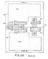
- FIG. 3 aseen in conjunction with FIG. 3 b , the preferred embodiment of the invention that represents one physical embodiment of the new pixel architecture can be appreciated. Other specific physical embodiments are realizable and should be readily apparent to those skilled in the art.
- This new architecture seen in FIG. 3 a and FIG. 3 bgenerally referred to as 30 , envisions sharing electrical functions between pixels 11 , 12 , 21 , and 22 that are arranged as row adjacent pixels 11 , 12 and 21 , 22 and column adjacent column pixels 11 , 21 and 12 , 22 .
- FIG. 3 aillustrates a top view of pixel architecture 30 while FIG. 3 b provides a schematic representation of the device shown in FIG. 3 a .
- pixel architecture 30provides a shared floating diffusion 41 between row adjacent pixels 11 , 12 in row 1 , and a shared floating diffusion 42 between row adjacent pixels 21 , 22 .
- Amplifier 32is preferably a source follower transistor configuration that is shared between all four of the shared pixels 11 , 12 , 21 , and 22 , as is row select transistor 35 , and reset transistor 36 .
- the row select signal bus 35 for both rows 1 , 2is the same, and the column output bus 87 for both columns a, b is actually the same.
- Image signal separationis achieved by having separate transfer gates 51 , 52 , 61 and 62 for each of the adjacent pixels 11 , 12 , 21 , and 22 . Separate transfer gate buses for every other pixel within a row, and a 1:2 column bus de-multiplexing scheme for each pair of columns.
- FIG. 4is a timing diagram detailing one mode of operation of this new architecture in conjunction with FIG. 3 a and FIG. 3 b .
- the image sensor 30is powered up in its reset state, with all the transfer gates 51 , 52 , TG 2 b 61 and 62 as well as the reset gate 37 turned on. Integration of row 1 begins by turning 52 off, which begins the integration for the odd pixels in row 1 , which includes pixel 12 . A predetermined time later transfer gate 51 is turned off, which begins the integration of the even pixels within row 1 which would include pixel 11 as illustrated. Once row 1 has integrated for the desired period of time row select gate 35 , and the column A transistor 81 is turned on, (column B transistor 91 is off).
- the reset level of the floating diffusion 41is then read by turning reset gate 37 off and strobing SHR 82 .
- Transfer gate 52is then pulsed on and the signal charge from photodetector PD 1 a 72 is transferred onto the floating diffusion 41 .
- the signal levelis then read out for the odd row photodetectors in Row 1 by strobing SHS 83 .
- pixel 11was still allowing photodetector 71 to integrate.
- the transfer of the integrated charge within pixel 11takes place when column A transistor 81 is turned off and the column B transistor 91 is turned on.
- Reset gate 37is turned on again, resetting the floating diffusion 41 .
- the reset levelis then read out by strobing SHR.
- transfer gate 51is pulsed on at the appropriate time, which is determined to be that amount of time such that photodetectors 72 and photodetectors 71 have the same integration time.
- the signal charge within photodetector PDB 2 in pixel 11is then transferred onto the floating diffusion 41 (this is the case for all of the even row photodetectors within Row 1 ).
- the signal levelis then read by strobing SHS 93 . Now all of the pixels in Row 1 have been read-out in to the bank of signal and reset capacitors. The line read-out is then done in the standard manner described in prior art CMOS imagers.
- This architectureprovides high fill factor and a resulting very small pixel size compared to prior art devices, since the active components are shared among four 4 photodetectors.
- One extra metal line per rowis required, to provide all the required transfer gates, but this takes up much less area than that occupied by the active components in both the per pixel amplifier scheme and the per 2 pixel amplifier scheme, discussed previously.
- this architecturealso has a temporal displacement of image capture of odd and even pixels within a given row.
Landscapes
- Engineering & Computer Science (AREA)
- Multimedia (AREA)
- Signal Processing (AREA)
- Solid State Image Pick-Up Elements (AREA)
- Transforming Light Signals Into Electric Signals (AREA)
Abstract
Description
This is a divisional of application Ser. No. 08/911,235, filed Aug. 15, 1997, now U.S. Pat. No. 6,107,655 entitled “ACTIVE PIXEL IMAGE SENSOR WITH SHARED AMPLIFIER READ-OUT” by Robert M. Guidash which is related to U.S. application Ser. No. 08/808,444 filed Feb. 28, 1997, now U.S. Pat. No. 6,160,281 by Robert M. Guidash and entitled, “ACTIVE PIXEL SENSOR WITH INTER-PIXEL SHARING”.
This invention relates to the field of solid state photo-sensors and imagers, and more specifically to semiconductor based imagers referred to as Active Pixel Sensors (APS).
Active Pixel Sensors (APS) are solid state imagers wherein each pixel contains a photo-sensing means with associated active circuitry elements. These active circuitry elements typically are means to perform a pixel reset function, or some means to transfer charge, means to perform a voltage conversion, or circuitry elements used in amplification. APS devices have been operated in a manner where each line or row of the imager is selected and then read out using a column select signal (analogous to a word and bit line in memory devices respectively). Prior art devices have been disclosed in which all of these components have been located entirely within a single pixel boundary.
Inclusion of these active circuit element components in each pixel reduces the fill factor for the pixel because it takes up area that could otherwise be used for the photodetector. This reduces the sensitivity and saturation signal of the sensor which in turn adversely affects the photographic speed and dynamic range of the sensor, performance parameters that are critical to obtaining good image quality. Additionally, inclusion of these active circuit elements within the pixel places a limitation on the minimum size of the pixel, which adversely affects the size and cost of the image sensor.
In order to build high resolution, small pixel APS devices, it is necessary to use sub μm CMOS processes in order to minimize the area of the pixel allocated to the row select transistor and other parts of the amplifier in the pixel. In essence, it takes a more technologically advanced and more costly process to realize the same resolution and sensitivity APS device when compared to a standard charge coupled device (CCD) sensor. However, APS devices have the advantages of single 5V supply operation, lower power consumption, x-y addressability, image windowing and the ability to effectively integrate signal processing electronics on-chip, when compared to CCD sensors.
A typical prior art APS pixel is shown in FIG.1. The pixel comprises aphotodetector 14, that can be constructed from either a photodiode or photogate technology, atransfer gate 15, afloating diffusion 16,reset transistor 18 with areset gate 19, a rowselect transistor 8 with a row select gate9, andsignal transistor 7 which is a source follower amplifier. Inclusion of all these components within a single pixel results in a reduction in the fill factor, sensitivity and minimum size of the pixel.
Referring to FIG. 2A in conjunction with FIG. 2B, one approach to providing an image sensor with the sensitivity of a CCD and the advantages of an APS device, is to improve the fill factor and sensitivity of an APS device by reducing the amount of area allotted to components within a single pixel while maintaining the desired features and functionality of the pixel architecture.
Referring to FIG. 2A in conjunction with FIG. 2B, U.S. patent application Ser. No. 08/808,444, entitled “Active Pixel Sensor With Inter-Pixel Function Sharing” by Guidash discloses a manner in which fill factors for APS devices can be increased. This prior art device of Guidash teaches the sharing of various components typically employed within an Active Pixel Sensor. Sharing of the floating diffusion, source follow amplifier, row select transistor, and reset transistor between two row adjacent photodetectors and transfer gates are disclosed here to assist in increasing the fill factor of the pixel architecture. The basic concept utilized by Guidash for increasing fill factor is the fact that a row at a time is read out during operation of the sensor. Accordingly, Guidash was able to provide a single floatingdiffusion 26 and asingle amplifier 27 for pixels located in two adjacent rows, instead of requiring one for every pixel as in the APS device shown in FIG.1. Since only one row is read out at a time, a single floatingdiffusion 26,reset transistor 28, rowselect transistor 29 and signal transistor27 (typically a source follower transistor) can be used for two adjacent pixels in separate rows.
While allowing for the sharing of components and increasing the fill factors within active pixel sensors, the device shown in FIG. 2 does not allow for the combining of function between both rows and columns, and accordingly the increase in fill factor that would result from such an architecture.
It should be readily apparent from the foregoing discussion that there remains a need within the art for an APS architecture that will allow for the combining of electrical functions between row as well as column pixels and the resulting increase in fill factor.
This invention addresses the aforementioned problems within prior art Active Pixel Sensor (APS) devices. It comprises a pixel and column circuitry architecture innovation that provides a higher fill factor pixel or a smaller pixel. By sharing components between adjacent columns and adjacent rows, components can be shared by four (4) separate photodetectors and transfer gates instead of two (2). This invention provides a means to further improve fill factor and further diminish the minimum pixel size by sharing the aforementioned components additionally between two column adjacent photodetectors and transfer gates, so that these components are now shared by four separate photodetectors and transfer gates, while maintaining the ability to selectively address specific pixels of the APS device.
Briefly summarized, according to one aspect of the present invention is an image sensor having a plurality of pixels arranged in a series of rows and columns comprising: a semiconductor material of a first conductivity type having at least two adjacent row pixels and at least two adjacent column pixels formed within the substrate, and at least one electrical function integrated within the adjacent pixels that is shared between the adjacent pixels.
These and other aspects, objects, features, and advantages of the present invention will be more clearly understood and appreciated from a review of the following detailed description of the preferred embodiments and appended claims, and by reference to the accompanying drawings.
The present invention has the following advantages:
High fill factor, sensitivity and saturation signal for the same pixel size.
Smaller pixel and device size for the same fill factor, providing a lower cost device.
FIG. 1A is a top view of a prior art pixel;
FIG. 1B is a schematic drawing of pixel shown in FIG. 1A.;
FIG. 2A is a top view of a prior art pixel with shared functionality;
FIG. 2B is a schematic view of the prior art pixel with shared functionality shown in FIG. 2A;
FIG. 3A is a top view of the pixel architecture with shared functionality as envisioned by the present invention;
FIG. 3B is a schematic view of the pixel architecture shown in FIG. 3A; and
FIG. 4 is a timing diagram illustrating the operation of the present invention.
To facilitate understanding, identical reference numerals have been used, where possible, to designate identical elements that are common to the figures.
I have discovered a pixel architecture wherein a smaller pixel size can be achieved by sharing functions between the adjacent pixels resulting in a smaller overall sensor device while still retaining as large a fill factor as larger sized sensor devices. This results in a lower cost device with a pixel size as large as existing prior art devices and having a higher fill factor with increased sensitivity and saturation signal is achieved.
Referring to FIG. 3aseen in conjunction with FIG. 3b, the preferred embodiment of the invention that represents one physical embodiment of the new pixel architecture can be appreciated. Other specific physical embodiments are realizable and should be readily apparent to those skilled in the art. This new architecture seen in FIG. 3aand FIG. 3b, generally referred to as30, envisions sharing electrical functions betweenpixels adjacent pixels adjacent column pixels pixel architecture 30 while FIG. 3bprovides a schematic representation of the device shown in FIG. 3a. As can be seen,pixel architecture 30 provides a shared floatingdiffusion 41 between rowadjacent pixels 11,12 inrow 1, and a shared floatingdiffusion 42 between rowadjacent pixels Amplifier 32 is preferably a source follower transistor configuration that is shared between all four of the sharedpixels select transistor 35, and resettransistor 36.
As shown in FIG. 3aand FIG. 3b, the rowselect signal bus 35 for bothrows column output bus 87 for both columns a, b is actually the same. Image signal separation is achieved by havingseparate transfer gates adjacent pixels
Referring now to FIG. 4 which is a timing diagram detailing one mode of operation of this new architecture in conjunction with FIG. 3aand FIG. 3b, Theimage sensor 30 is powered up in its reset state, with all thetransfer gates reset gate 37 turned on. Integration ofrow 1 begins by turning52 off, which begins the integration for the odd pixels inrow 1, which includespixel 12. A predetermined timelater transfer gate 51 is turned off, which begins the integration of the even pixels withinrow 1 which would include pixel11 as illustrated. Oncerow 1 has integrated for the desired period of time rowselect gate 35, and thecolumn A transistor 81 is turned on, (column B transistor 91 is off). The reset level of the floatingdiffusion 41 is then read by turningreset gate 37 off and strobing SHR82.Transfer gate 52 is then pulsed on and the signal charge from photodetector PD1a72 is transferred onto the floatingdiffusion 41. The signal level is then read out for the odd row photodetectors inRow 1 by strobing SHS83. While the integrated charge forpixel 12 was being transferred, pixel11 was still allowingphotodetector 71 to integrate. The transfer of the integrated charge within pixel11, takes place whencolumn A transistor 81 is turned off and thecolumn B transistor 91 is turned on.Reset gate 37 is turned on again, resetting the floatingdiffusion 41. The reset level is then read out by strobing SHR. Next,transfer gate 51 is pulsed on at the appropriate time, which is determined to be that amount of time such that photodetectors72 andphotodetectors 71 have the same integration time. The signal charge within photodetector PDB2 in pixel11 is then transferred onto the floating diffusion41 (this is the case for all of the even row photodetectors within Row1). The signal level is then read by strobing SHS93. Now all of the pixels inRow 1 have been read-out in to the bank of signal and reset capacitors. The line read-out is then done in the standard manner described in prior art CMOS imagers. This same sequence is then done forRow 2, where all of the signals are the same excepttransfer gate photodetectors pixels
This architecture provides high fill factor and a resulting very small pixel size compared to prior art devices, since the active components are shared among four 4 photodetectors. One extra metal line per row is required, to provide all the required transfer gates, but this takes up much less area than that occupied by the active components in both the per pixel amplifier scheme and the per 2 pixel amplifier scheme, discussed previously. There are 3 extra timing and control signals required and 2 additional transistors per column required. However, these do not impact the pixel or image array area since they are incorporated in the CMOS logic outside of the image array. In addition to the temporal displacement of image capture on a per row basis, this architecture also has a temporal displacement of image capture of odd and even pixels within a given row. This time is very short however, (especially compared to the row to row temporal displacement), on the order of a few hundred nanoseconds, and will not produce any image capture artifacts. Because there is an extra sequence of sample and holds, (SHR and SHS strobes), the minimum line time is slightly longer for this new architecture, which will incrementally diminish the maximum frame rate for video applications.
The invention has been described in detail with particular reference to certain preferred embodiments thereof, but it will be understood that variations and modifications can be effected within the spirit and scope of the invention.
1row 1
2row 2
3row 3
4row 4
7 signal transistor
8 row select transistor
9 row select gate
10 prior art pixel
11 pixel
12 pixel
14 photodetector
15 transfergate
16 floating diffusion
18 reset transistor
19 reset gate
21 pixel
22 pixel
24 photodetector
26 floating diffusion
27 signal transistor
28 reset transistor
29 select transistor
30 shared row and column circuit pixels
32 floating diffusion amplifier
34 row select transistor
35 row select gate
36 reset transistor
37 reset gate
38 column output bus
41 floating diffusion
42 floating diffusion
51 transfer gate
52 transfer gate
61 transfer gate
62 transfer gate
71 photodetector
72 photodetector
73 photodetector
74 photodetector
80 column sample hold
81 transistor
82 sample and hold reset
83 sample and hold signal
87 output bus
90 column sample hold
91 transistor
92 sample and hold reset
93 sample and hold signal
Claims (21)
1. A method of making solid state image sensing devices comprising the steps of:
(a) providing a semiconductor substrate having a plurality of pixels formed in columns and rows; and
(b) further providing within at least two row adjacent and two column adjacent pixels at least one electrical function that is shared between the adjacent pixels with the at least one electrical function being an electrical component having at least a portion of the electrical component structurally located within the pixel boundary of another of the adjacent pixels.
2. The method ofclaim 1 wherein step (b) further comprises providing the shared function such that it is formed essentially equally between the adjacent pixels.
3. The method ofclaim 1 wherein step (b) includes providing the shared function such that it performs a first function for one of the adjacent pixels and a second function for the other adjacent pixel.
4. The method ofclaim 1 wherein step (b) includes providing an electrical contact as the shared function.
5. The method ofclaim 4 wherein step (b) further comprises providing the electrical contact selected from one of the following contacts (a photogate contact, a transfer gate contact, a reset gate contact, a row select gate contact, an amplifier drain contact, an output node contact, a floating diffusion contact, a reset drain contact, a lateral overflow gate contact, an overflow drain contact or an amplifier contact).
6. The method ofclaim 1 wherein step (b) further comprises providing as the shared function a shared contact region but not a shared electrical component between the adjacent pixels.
7. The method ofclaim 1 wherein step (b) further comprises providing as the shared function both a shared contact region and a shared electrical component.
8. The method ofclaim 1 wherein step (b) further comprises providing as the electrical function an electrical component selected from one of the following components (a transfer gate, a reset gate, a row select gate, an amplifier drain, an output node, a floating diffusion, a reset drain, a lateral overflow gate, an overflow drain or an amplifier).
9. The method ofclaim 1 wherein step (b) further comprises providing a voltage supply of one pixel that is also used as an overflow drain for the adjacent pixel.
10. A method of making solid state image sensing devices comprising the steps of:
(a) providing a semiconductor substrate having a plurality of pixels formed in columns and rows; and
(b) additionally providing at least two row adjacent and two column adjacent pixels with one electrical function that is shared between at least two of the adjacent pixels, wherein the shared function is an electrical contact with at least a portion of the electrical contact being structurally located within the pixel boundary of another of the adjacent pixels.
11. The method ofclaim 10 wherein step (b) further comprises providing the shared function such that it is formed essentially equally between at least two of the adjacent pixels.
12. The method ofclaim 10 wherein step (b) includes providing the shared function such that it performs a first function for one of the adjacent pixels and a second function for the other adjacent pixel.
13. The method ofclaim 10 wherein step (b) further includes providing an electrical component as the shared function.
14. The method ofclaim 13 wherein step (b) further includes providing a portion of the electrical component that is structurally located within at least two adjacent pixels.
15. The method ofclaim 10 wherein step (b) further comprises providing the electrical contact selected from one of the following contacts (a photogate contact, a transfer gate contact, a reset gate contact, a row select gate contact, an amplifier drain contact, an output node contact, a floating diffusion contact, a reset drain contact, a lateral overflow gate contact, an overflow drain contact or an amplifier contact).
16. The method ofclaim 10 wherein step (b) further comprises providing as the shared function a shared contact region but not a shared electrical component between the adjacent pixels.
17. The method ofclaim 10 wherein step (b) further comprises providing as the shared function both a shared contact region and a shared electrical component.
18. The method ofclaim 10 wherein step (b) further comprises providing as the electrical function an electrical component selected from one of the following components (a transfer gate, a reset gate, a row select gate, an amplifier drain, an output node, a floating diffusion, a reset drain, a lateral overflow gate, an overflow drain or an amplifier).
19. The method ofclaim 10 wherein step (b) further comprises providing a voltage supply of one pixel that is also used as an overflow drain for the adjacent pixel.
20. The method ofclaim 10 wherein step (b) further comprises providing an electrical component as the electrical function with at least a portion of the electrical component is structurally located within the pixel boundary of another of the adjacent pixels.
21. A solid state image sensing product formed from a process comprising the steps of:
providing a semiconductor substrate having a plurality of pixels formed in columns and rows; and
further providing within at least two row adjacent and two column adjacent pixels with at least one electrical function that is shared between at least two of the adjacent pixels such that the electrical function is structurally located within the at least two adjacent pixels.
Priority Applications (1)
| Application Number | Priority Date | Filing Date | Title |
|---|---|---|---|
| US09/515,830US6352869B1 (en) | 1997-08-15 | 2000-02-29 | Active pixel image sensor with shared amplifier read-out |
Applications Claiming Priority (2)
| Application Number | Priority Date | Filing Date | Title |
|---|---|---|---|
| US08/911,235US6107655A (en) | 1997-08-15 | 1997-08-15 | Active pixel image sensor with shared amplifier read-out |
| US09/515,830US6352869B1 (en) | 1997-08-15 | 2000-02-29 | Active pixel image sensor with shared amplifier read-out |
Related Parent Applications (1)
| Application Number | Title | Priority Date | Filing Date |
|---|---|---|---|
| US08/911,235DivisionUS6107655A (en) | 1997-08-15 | 1997-08-15 | Active pixel image sensor with shared amplifier read-out |
Publications (1)
| Publication Number | Publication Date |
|---|---|
| US6352869B1true US6352869B1 (en) | 2002-03-05 |
Family
ID=25429949
Family Applications (2)
| Application Number | Title | Priority Date | Filing Date |
|---|---|---|---|
| US08/911,235Expired - LifetimeUS6107655A (en) | 1997-08-15 | 1997-08-15 | Active pixel image sensor with shared amplifier read-out |
| US09/515,830Expired - LifetimeUS6352869B1 (en) | 1997-08-15 | 2000-02-29 | Active pixel image sensor with shared amplifier read-out |
Family Applications Before (1)
| Application Number | Title | Priority Date | Filing Date |
|---|---|---|---|
| US08/911,235Expired - LifetimeUS6107655A (en) | 1997-08-15 | 1997-08-15 | Active pixel image sensor with shared amplifier read-out |
Country Status (6)
| Country | Link |
|---|---|
| US (2) | US6107655A (en) |
| EP (1) | EP0898312B1 (en) |
| JP (1) | JP4267095B2 (en) |
| KR (1) | KR100637945B1 (en) |
| DE (1) | DE69835989T2 (en) |
| TW (1) | TW373399B (en) |
Cited By (61)
| Publication number | Priority date | Publication date | Assignee | Title |
|---|---|---|---|---|
| US20010026321A1 (en)* | 2000-03-29 | 2001-10-04 | Hiroshige Goto | Amplification type solid-state imaging device having a potential detecting circuit for each unit cell and high-speed readout method thereof |
| US6633334B1 (en)* | 1997-12-26 | 2003-10-14 | Canon Kabushiki Kaisha | Solid-state image pickup device with optimum layout of building components around a photoelectric conversion portion |
| US20040051164A1 (en)* | 2002-08-29 | 2004-03-18 | Fossum Eric R. | Two-transistor pixel with buried reset channel and method of formation |
| US20040096124A1 (en)* | 2002-11-15 | 2004-05-20 | Junichi Nakamura | Wide dynamic range pinned photodiode active pixel sensor (aps) |
| US6750514B2 (en)* | 2001-11-07 | 2004-06-15 | Koninklijke Philips Electronics N.V. | Display having universal active matrix |
| US20040159861A1 (en)* | 2003-02-13 | 2004-08-19 | Matsushita Electric Industrial Co., Ltd. | Solid state imaging apparatus, method for driving the same and camera using the same |
| US20040169127A1 (en)* | 2002-08-29 | 2004-09-02 | Narumi Ohkawa | Semiconductor device for reading signal from photodiode via transistors |
| US20040252215A1 (en)* | 2003-05-30 | 2004-12-16 | Matsushita Electric Industrial Co., Ltd. | Solid state imaging device |
| US20050104094A1 (en)* | 2003-09-30 | 2005-05-19 | Kabushiki Kaisha Toshiba | Solid-state imaging device and electronic still camera |
| US20050110884A1 (en)* | 2003-11-26 | 2005-05-26 | Altice Peter P.Jr. | Image sensor with a capacitive storage node linked to transfer gate |
| US20050110885A1 (en)* | 2003-11-26 | 2005-05-26 | Altice Peter P.Jr. | Image sensor with a gated storage node linked to transfer gate |
| US20050110093A1 (en)* | 2003-11-26 | 2005-05-26 | Altice Peter P.Jr. | Anti-blooming storage pixel |
| US20050237405A1 (en)* | 2004-04-27 | 2005-10-27 | Fujitsu Limited | Solid-state image sensor |
| US20060038904A1 (en)* | 2004-08-11 | 2006-02-23 | Yoshiharu Kudoh | Solid-state imaging device and imaging apparatus |
| US20060043440A1 (en)* | 2004-09-01 | 2006-03-02 | Canon Kabushiki Kaisha | Imaging device and imaging system |
| US20060063295A1 (en)* | 2004-09-22 | 2006-03-23 | Kazunobu Kuwazawa | Solid-state image pickup device and driving method thereof |
| US20060208163A1 (en)* | 2004-02-04 | 2006-09-21 | Omnivision Technologies, Inc. | CMOS image sensor using shared transistors between pixels having mirror symmetry |
| US20060240631A1 (en)* | 2005-04-22 | 2006-10-26 | Sharp Kabushiki Kaisha | Method for manufacturing a solid-state image capturing device and electric information device |
| US20060249653A1 (en)* | 2005-05-06 | 2006-11-09 | Gazeley William G | Pixel with spatially varying metal route positions |
| US20060256221A1 (en)* | 2005-05-11 | 2006-11-16 | Micron Technology, Inc. | High fill factor multi-way shared pixel |
| US20060255381A1 (en)* | 2005-05-10 | 2006-11-16 | Micron Technology, Inc. | Pixel with gate contacts over active region and method of forming same |
| US20060267052A1 (en)* | 2005-05-11 | 2006-11-30 | Micron Technology, Inc. | Split trunk pixel layout |
| US20060284177A1 (en)* | 2005-06-15 | 2006-12-21 | Magnachip Semiconductor Ltd. | Image sensor with compact pixel layout |
| US20070007559A1 (en)* | 2005-07-09 | 2007-01-11 | Duck-Hyung Lee | Image sensors including active pixel sensor arrays |
| US20070012964A1 (en)* | 2005-07-12 | 2007-01-18 | Micron Technology, Inc. | Method and apparatus providing capacitor on an electrode of an imager photosensor |
| US20070013797A1 (en)* | 2005-07-12 | 2007-01-18 | Micron Technology, Inc. | Dual conversion gain gate and capacitor and HDR combination |
| US20070023798A1 (en)* | 2005-08-01 | 2007-02-01 | Micron Technology, Inc. | Dual conversion gain gate and capacitor combination |
| US20070034884A1 (en)* | 2005-08-11 | 2007-02-15 | Micron Technology, Inc. | Pixel cells in a honeycomb arrangement |
| US20070035649A1 (en)* | 2005-08-10 | 2007-02-15 | Micron Technology, Inc. | Image pixel reset through dual conversion gain gate |
| US20070040922A1 (en)* | 2005-08-22 | 2007-02-22 | Micron Technology, Inc. | HDR/AB on multi-way shared pixels |
| US20070046796A1 (en)* | 2005-08-30 | 2007-03-01 | Micron Technology, Inc. | Method and apparatus providing a two-way shared storage gate on a four-way shared pixel |
| US20070045679A1 (en)* | 2005-08-26 | 2007-03-01 | Micron Technology, Inc. | Implanted isolation region for imager pixels |
| US20070045514A1 (en)* | 2005-08-30 | 2007-03-01 | Micron Technology, Inc. | Method and apparatus providing a two-way shared storage gate on a four-way shared pixel |
| US20070052055A1 (en)* | 2005-08-24 | 2007-03-08 | Micron Technology, Inc. | Capacitor over red pixel |
| KR100690169B1 (en)* | 2005-10-25 | 2007-03-08 | 매그나칩 반도체 유한회사 | CMOS image sensor |
| US20070058062A1 (en)* | 2005-09-13 | 2007-03-15 | Sougo Ohta | Solid-state image pickup device |
| US20070164332A1 (en)* | 2006-01-13 | 2007-07-19 | Kee-Hyun Paik | Shared-pixel-type image sensors for controlling capacitance of floating diffusion region |
| US20070210239A1 (en)* | 2006-03-10 | 2007-09-13 | Samsung Electronics Co., Ltd. | Image sensor with high fill factor pixels and method for forming an image sensor |
| US20070252182A1 (en)* | 2006-04-27 | 2007-11-01 | Beck Jeffery S | Buried-gated photodiode device and method for configuring and operating same |
| US20080055441A1 (en)* | 2006-08-29 | 2008-03-06 | Micron Technology, Inc. | Method, apparatus and system providing a storage gate pixel with high dynamic range |
| WO2008032933A1 (en)* | 2006-09-11 | 2008-03-20 | Siliconfile Technologies Inc. | Unit pixel including three transistors and pixel array including the unit pixels |
| US20080088724A1 (en)* | 2006-10-13 | 2008-04-17 | Sony Corporation | Solid-state imaging device, imaging apparatus and camera |
| US20080237450A1 (en)* | 2006-11-01 | 2008-10-02 | International Business Machines Corporation | Structure for a cmos imaging sensor |
| US20080246869A1 (en)* | 2002-08-29 | 2008-10-09 | Alexander Krymski | Differential readout from pixels in CMOS sensor |
| US20090057537A1 (en)* | 2005-05-06 | 2009-03-05 | Micron Technology, Inc. | Pixel with spatially varying sensor positions |
| US20090180010A1 (en)* | 2008-01-14 | 2009-07-16 | Adkisson James W | Low lag transfer gate device |
| US20090179232A1 (en)* | 2008-01-14 | 2009-07-16 | Adkisson James W | Low lag transfer gate device |
| US20100045834A1 (en)* | 2005-10-21 | 2010-02-25 | Sony Corporation | Solid-state imaging apparatus and camera |
| US7671314B2 (en) | 2005-07-09 | 2010-03-02 | Samsung Electronics Co., Ltd. | Image sensor including active pixel sensor array with photoelectric conversion region |
| US20100134664A1 (en)* | 2008-12-01 | 2010-06-03 | Canon Kabushiki Kaisha | Solid-state imaging apparatus, and imaging system using the same |
| US20100134648A1 (en)* | 2007-02-09 | 2010-06-03 | Sony Corporation | Solid-state image pickup device and camera system |
| US20100148037A1 (en)* | 2008-12-12 | 2010-06-17 | Jan Bogaerts | Pixel array with shared readout circuitry |
| US20110025892A1 (en)* | 2009-08-03 | 2011-02-03 | International Business Machines Corporation | Image sensor pixel structure employing a shared floating diffusion |
| US20110024809A1 (en)* | 2009-07-31 | 2011-02-03 | James Robert Janesick | Ring pixel for cmos imagers |
| CN1893541B (en)* | 2005-07-09 | 2012-07-04 | 三星电子株式会社 | Image sensors including active pixel sensor arrays and system |
| US20140125840A1 (en)* | 1998-04-30 | 2014-05-08 | Canon Kabushiki Kaisha | Rrangement of circuits in pixels, each circuit shared by a plurality of pixels, in image sensing appratus |
| US8723093B2 (en) | 2011-01-10 | 2014-05-13 | Alexander Krymski | Image sensors and methods with shared control lines |
| US20140131556A1 (en)* | 2012-11-12 | 2014-05-15 | Canon Kabushiki Kaisha | Imaging apparatus, and imaging system |
| US9369648B2 (en) | 2013-06-18 | 2016-06-14 | Alexander Krymski | Image sensors, methods, and pixels with tri-level biased transfer gates |
| US10608037B2 (en) | 2016-12-27 | 2020-03-31 | Samsung Electronics Co., Ltd. | Image sensor and electronic apparatus including the same |
| US11282891B2 (en) | 2003-11-26 | 2022-03-22 | Samsung Electronics Co., Ltd. | Image sensor with a gated storage node linked to transfer gate |
Families Citing this family (80)
| Publication number | Priority date | Publication date | Assignee | Title |
|---|---|---|---|---|
| US6815791B1 (en)* | 1997-02-10 | 2004-11-09 | Fillfactory | Buried, fully depletable, high fill factor photodiodes |
| US7199410B2 (en)* | 1999-12-14 | 2007-04-03 | Cypress Semiconductor Corporation (Belgium) Bvba | Pixel structure with improved charge transfer |
| US6107655A (en)* | 1997-08-15 | 2000-08-22 | Eastman Kodak Company | Active pixel image sensor with shared amplifier read-out |
| JPH11274454A (en)* | 1998-03-19 | 1999-10-08 | Canon Inc | Solid-state imaging device and method of forming the same |
| JP3410016B2 (en)* | 1998-03-31 | 2003-05-26 | 株式会社東芝 | Amplification type solid-state imaging device |
| KR19990084630A (en)* | 1998-05-08 | 1999-12-06 | 김영환 | CMOS image sensor and its driving method |
| FR2781929B1 (en)* | 1998-07-28 | 2002-08-30 | St Microelectronics Sa | IMAGE SENSOR WITH PHOTODIODE ARRAY |
| US6956605B1 (en)* | 1998-08-05 | 2005-10-18 | Canon Kabushiki Kaisha | Image pickup apparatus |
| US6239456B1 (en) | 1998-08-19 | 2001-05-29 | Photobit Corporation | Lock in pinned photodiode photodetector |
| US6734906B1 (en)* | 1998-09-02 | 2004-05-11 | Canon Kabushiki Kaisha | Image pickup apparatus with photoelectric conversion portions arranged two dimensionally |
| US6657665B1 (en)* | 1998-12-31 | 2003-12-02 | Eastman Kodak Company | Active Pixel Sensor with wired floating diffusions and shared amplifier |
| US6750912B1 (en)* | 1999-09-30 | 2004-06-15 | Ess Technology, Inc. | Active-passive imager pixel array with small groups of pixels having short common bus lines |
| EP1102323B1 (en)* | 1999-11-19 | 2012-08-15 | CSEM Centre Suisse d'Electronique et de Microtechnique SA - Recherche et Développement | Method for detecting electromagnetic radiation using an optoelectronic sensor |
| KR100683396B1 (en)* | 1999-12-28 | 2007-02-15 | 매그나칩 반도체 유한회사 | Pixel array scanning method of image sensor |
| US6710804B1 (en)* | 2000-01-18 | 2004-03-23 | Eastman Kodak Company | CMOS active pixel image sensor with extended dynamic range and sensitivity |
| JP4721380B2 (en)* | 2000-04-14 | 2011-07-13 | キヤノン株式会社 | Solid-state imaging device and imaging system |
| JP4246890B2 (en)* | 2000-06-26 | 2009-04-02 | 株式会社東芝 | Solid-state imaging device |
| FR2820882B1 (en) | 2001-02-12 | 2003-06-13 | St Microelectronics Sa | THREE TRANSISTOR PHOTODETECTOR |
| FR2820883B1 (en) | 2001-02-12 | 2003-06-13 | St Microelectronics Sa | HIGH CAPACITY PHOTODIODE |
| FR2824665B1 (en)* | 2001-05-09 | 2004-07-23 | St Microelectronics Sa | CMOS TYPE PHOTODETECTOR |
| JP2003007995A (en)* | 2001-06-20 | 2003-01-10 | Iwate Toshiba Electronics Co Ltd | CMOS image sensor |
| JP2003258231A (en)* | 2002-03-05 | 2003-09-12 | Sony Corp | Solid-state imaging device |
| US7361881B2 (en)* | 2002-03-13 | 2008-04-22 | Oy Ajat Ltd | Ganged detector pixel, photon/pulse counting radiation imaging device |
| JP2004134867A (en)* | 2002-10-08 | 2004-04-30 | Canon Inc | Solid-state imaging device, driving method thereof, and imaging system |
| US20040113151A1 (en)* | 2002-10-11 | 2004-06-17 | Kabushiki Kaisha Toshiba | CMOS image sensor |
| US20050128327A1 (en)* | 2003-12-10 | 2005-06-16 | Bencuya Selim S. | Device and method for image sensing |
| JP4647404B2 (en)* | 2004-07-07 | 2011-03-09 | 三星電子株式会社 | Manufacturing method of image sensor having photodiode self-aligned while being superimposed on transfer gate electrode |
| DE602004030958D1 (en) | 2004-07-20 | 2011-02-17 | Fujitsu Semiconductor Ltd | CMOS imaging device |
| JP2006147708A (en)* | 2004-11-17 | 2006-06-08 | Omron Corp | Imaging device |
| KR100674925B1 (en)* | 2004-12-07 | 2007-01-26 | 삼성전자주식회사 | Honeycomb Active Pixel Sensor |
| US20060125947A1 (en)* | 2004-12-09 | 2006-06-15 | Packer Jimmy L | Imaging with clustered photosite arrays |
| US7750958B1 (en) | 2005-03-28 | 2010-07-06 | Cypress Semiconductor Corporation | Pixel structure |
| US7808022B1 (en) | 2005-03-28 | 2010-10-05 | Cypress Semiconductor Corporation | Cross talk reduction |
| US7361877B2 (en) | 2005-05-27 | 2008-04-22 | Eastman Kodak Company | Pinned-photodiode pixel with global shutter |
| US8253214B2 (en) | 2005-06-02 | 2012-08-28 | Omnivision Technologies, Inc. | CMOS shared amplifier pixels with output signal wire below floating diffusion interconnect for reduced floating diffusion capacitance |
| US7449736B2 (en) | 2005-07-12 | 2008-11-11 | Micron Technology, Inc. | Pixel with transfer gate with no isolation edge |
| KR100787938B1 (en)* | 2005-07-15 | 2007-12-24 | 삼성전자주식회사 | CMOS image sensor with shared active pixel sensor structure and its driving method |
| US8139130B2 (en) | 2005-07-28 | 2012-03-20 | Omnivision Technologies, Inc. | Image sensor with improved light sensitivity |
| US8274715B2 (en) | 2005-07-28 | 2012-09-25 | Omnivision Technologies, Inc. | Processing color and panchromatic pixels |
| JP5130614B2 (en)* | 2005-09-22 | 2013-01-30 | ソニー株式会社 | Semiconductor image sensor |
| US20070069260A1 (en)* | 2005-09-28 | 2007-03-29 | Eastman Kodak Company | Photodetector structure for improved collection efficiency |
| US7875916B2 (en)* | 2005-09-28 | 2011-01-25 | Eastman Kodak Company | Photodetector and n-layer structure for improved collection efficiency |
| US7728277B2 (en)* | 2005-11-16 | 2010-06-01 | Eastman Kodak Company | PMOS pixel structure with low cross talk for active pixel image sensors |
| KR100778854B1 (en)* | 2005-12-29 | 2007-11-22 | 동부일렉트로닉스 주식회사 | CMOS image sensor and its manufacturing method |
| US7916362B2 (en) | 2006-05-22 | 2011-03-29 | Eastman Kodak Company | Image sensor with improved light sensitivity |
| JP4887079B2 (en)* | 2006-06-06 | 2012-02-29 | 富士フイルム株式会社 | Photoelectric conversion film stack type solid-state imaging device |
| US8031258B2 (en) | 2006-10-04 | 2011-10-04 | Omnivision Technologies, Inc. | Providing multiple video signals from single sensor |
| KR100821469B1 (en) | 2006-10-13 | 2008-04-11 | 매그나칩 반도체 유한회사 | Compact CMOS image sensor with improved color crosstalk and method of manufacturing the same |
| US8184190B2 (en)* | 2006-11-28 | 2012-05-22 | Youliza, Gehts B.V. Limited Liability Company | Simultaneous global shutter and correlated double sampling read out in multiple photosensor pixels |
| US8013920B2 (en) | 2006-12-01 | 2011-09-06 | Youliza, Gehts B.V. Limited Liability Company | Imaging system for creating an image of an object |
| WO2008088981A1 (en) | 2007-01-11 | 2008-07-24 | Micron Technology, Inc. | Missing pixel architecture |
| US7915702B2 (en)* | 2007-03-15 | 2011-03-29 | Eastman Kodak Company | Reduced pixel area image sensor |
| US20080296639A1 (en)* | 2007-06-01 | 2008-12-04 | Dalsa Corporation | Semiconductor image sensor array device, apparatus comprising such a device and method for operating such a device |
| KR100835894B1 (en)* | 2007-06-18 | 2008-06-09 | (주)실리콘화일 | Pixel array and image sensor with wide dynamic range and excellent color reproduction and resolution |
| US7960768B2 (en)* | 2008-01-17 | 2011-06-14 | Aptina Imaging Corporation | 3D backside illuminated image sensor with multiplexed pixel structure |
| JP4952601B2 (en) | 2008-02-04 | 2012-06-13 | 日本テキサス・インスツルメンツ株式会社 | Solid-state imaging device |
| US7745773B1 (en)* | 2008-04-11 | 2010-06-29 | Foveon, Inc. | Multi-color CMOS pixel sensor with shared row wiring and dual output lines |
| JP5058090B2 (en)* | 2008-07-18 | 2012-10-24 | 株式会社東芝 | Solid-state imaging device |
| US8476567B2 (en) | 2008-09-22 | 2013-07-02 | Semiconductor Components Industries, Llc | Active pixel with precharging circuit |
| US8618458B2 (en) | 2008-11-07 | 2013-12-31 | Omnivision Technologies, Inc. | Back-illuminated CMOS image sensors |
| US8338868B2 (en)* | 2008-12-03 | 2012-12-25 | Electronics And Telecommunications Research Institute | Shared photodiode image sensor |
| US20100140668A1 (en)* | 2008-12-08 | 2010-06-10 | Stevens Eric G | Shallow trench isolation regions in image sensors |
| US20100148230A1 (en)* | 2008-12-11 | 2010-06-17 | Stevens Eric G | Trench isolation regions in image sensors |
| US20100148291A1 (en) | 2008-12-15 | 2010-06-17 | Tivarus Cristian A | Ultraviolet light filter layer in image sensors |
| JP2010199450A (en)* | 2009-02-27 | 2010-09-09 | Sony Corp | Manufacturing method of solid-state imaging device, solid-state imaging device, and electronic apparatus |
| US8130304B2 (en)* | 2009-07-24 | 2012-03-06 | Aptina Imaging Corporation | Image sensors with pixel charge summing |
| TWI559763B (en)* | 2009-10-01 | 2016-11-21 | 索尼半導體解決方案公司 | Image acquisition device and camera system |
| US8872953B2 (en)* | 2009-10-30 | 2014-10-28 | Sony Corporation | Solid-state imaging device, manufacturing method thereof, camera, and electronic device |
| US8318580B2 (en) | 2010-04-29 | 2012-11-27 | Omnivision Technologies, Inc. | Isolating wire bonding in integrated electrical components |
| US8748946B2 (en) | 2010-04-29 | 2014-06-10 | Omnivision Technologies, Inc. | Isolated wire bond in integrated electrical components |
| CN102544044B (en)* | 2012-02-01 | 2015-06-24 | 中国科学院上海高等研究院 | CMOS (Complementary Metal-oxide Semiconductor) image sensor and CMOS image sensing circuit system |
| CN102856332A (en)* | 2012-04-10 | 2013-01-02 | 天津大学 | Large-size four-transistor active pixel sensor (4T APS) for rapidly transferring charges |
| JP5813047B2 (en)* | 2013-04-26 | 2015-11-17 | キヤノン株式会社 | Imaging device and imaging system. |
| JP6366285B2 (en)* | 2014-01-30 | 2018-08-01 | キヤノン株式会社 | Solid-state imaging device |
| CN104867949A (en)* | 2014-02-21 | 2015-08-26 | 恒景科技股份有限公司 | Image sensor |
| US9190435B2 (en)* | 2014-03-09 | 2015-11-17 | Himax Imaging Limited | Shared active pixel sensor |
| CN104184969A (en)* | 2014-09-03 | 2014-12-03 | 北京思比科微电子技术股份有限公司 | Image sensor achieving improved black-level alignment |
| US9526468B2 (en) | 2014-09-09 | 2016-12-27 | General Electric Company | Multiple frame acquisition for exposure control in X-ray medical imagers |
| JP6587497B2 (en)* | 2014-10-31 | 2019-10-09 | 株式会社半導体エネルギー研究所 | Semiconductor device |
| DE102015109878B3 (en)* | 2015-06-19 | 2016-07-28 | Basler Ag | Correction of a patterned image defect |
Citations (14)
| Publication number | Priority date | Publication date | Assignee | Title |
|---|---|---|---|---|
| US4636865A (en) | 1984-04-27 | 1987-01-13 | Olympus Optical Co., Ltd. | Solid state image sensor |
| JPS63261744A (en) | 1987-04-20 | 1988-10-28 | Olympus Optical Co Ltd | solid-state imaging device |
| US5144447A (en)* | 1988-03-31 | 1992-09-01 | Hitachi, Ltd. | Solid-state image array with simultaneously activated line drivers |
| US5237190A (en) | 1992-07-31 | 1993-08-17 | Hualon Microelectronics Corporation | Charge-coupled-device color image sensor |
| US5243180A (en) | 1991-10-04 | 1993-09-07 | Samsung Electronics Co., Ltd. | Solid-state image sensor with paired photodiode connected to respective vertical ccd channels |
| US5280186A (en) | 1990-05-11 | 1994-01-18 | Gold Star Electron Co. | CCD image sensor with four phase clocking mechanism |
| US5338948A (en) | 1991-05-10 | 1994-08-16 | Photometrics, Ltd. | Charge-coupled device with open gate structure |
| US5418387A (en) | 1992-12-28 | 1995-05-23 | Kabushiki Kaisha Toshiba | Solid-state imaging device with nand cell structure |
| US5517043A (en) | 1994-10-25 | 1996-05-14 | Dalsa, Inc. | Split pixel interline transfer imaging device |
| US5600159A (en) | 1993-12-15 | 1997-02-04 | Kabushiki Kaisha Toshiba | Solid state image sensing device having facilitated output signal correction |
| EP0757476A2 (en) | 1995-08-02 | 1997-02-05 | Canon Kabushiki Kaisha | Solid state image pickup apparatus |
| EP0862219A2 (en) | 1997-02-28 | 1998-09-02 | Eastman Kodak Company | Active pixel sensor in which adjacent pixels share an integrated electrical element |
| US5867215A (en) | 1995-04-11 | 1999-02-02 | Eastman Kodak Company | Image sensor having multiple storage wells per pixel |
| US6107655A (en)* | 1997-08-15 | 2000-08-22 | Eastman Kodak Company | Active pixel image sensor with shared amplifier read-out |
- 1997
- 1997-08-15USUS08/911,235patent/US6107655A/ennot_activeExpired - Lifetime
- 1998
- 1998-06-26TWTW087110376Apatent/TW373399B/ennot_activeIP Right Cessation
- 1998-08-05DEDE69835989Tpatent/DE69835989T2/ennot_activeExpired - Lifetime
- 1998-08-05EPEP98202641Apatent/EP0898312B1/ennot_activeExpired - Lifetime
- 1998-08-12KRKR1019980032715Apatent/KR100637945B1/ennot_activeExpired - Lifetime
- 1998-08-13JPJP22879598Apatent/JP4267095B2/ennot_activeExpired - Lifetime
- 2000
- 2000-02-29USUS09/515,830patent/US6352869B1/ennot_activeExpired - Lifetime
Patent Citations (15)
| Publication number | Priority date | Publication date | Assignee | Title |
|---|---|---|---|---|
| US4636865A (en) | 1984-04-27 | 1987-01-13 | Olympus Optical Co., Ltd. | Solid state image sensor |
| JPS63261744A (en) | 1987-04-20 | 1988-10-28 | Olympus Optical Co Ltd | solid-state imaging device |
| US5144447A (en)* | 1988-03-31 | 1992-09-01 | Hitachi, Ltd. | Solid-state image array with simultaneously activated line drivers |
| US5280186A (en) | 1990-05-11 | 1994-01-18 | Gold Star Electron Co. | CCD image sensor with four phase clocking mechanism |
| US5338948A (en) | 1991-05-10 | 1994-08-16 | Photometrics, Ltd. | Charge-coupled device with open gate structure |
| US5243180A (en) | 1991-10-04 | 1993-09-07 | Samsung Electronics Co., Ltd. | Solid-state image sensor with paired photodiode connected to respective vertical ccd channels |
| US5237190A (en) | 1992-07-31 | 1993-08-17 | Hualon Microelectronics Corporation | Charge-coupled-device color image sensor |
| US5418387A (en) | 1992-12-28 | 1995-05-23 | Kabushiki Kaisha Toshiba | Solid-state imaging device with nand cell structure |
| US5600159A (en) | 1993-12-15 | 1997-02-04 | Kabushiki Kaisha Toshiba | Solid state image sensing device having facilitated output signal correction |
| US5517043A (en) | 1994-10-25 | 1996-05-14 | Dalsa, Inc. | Split pixel interline transfer imaging device |
| US5867215A (en) | 1995-04-11 | 1999-02-02 | Eastman Kodak Company | Image sensor having multiple storage wells per pixel |
| EP0757476A2 (en) | 1995-08-02 | 1997-02-05 | Canon Kabushiki Kaisha | Solid state image pickup apparatus |
| EP0862219A2 (en) | 1997-02-28 | 1998-09-02 | Eastman Kodak Company | Active pixel sensor in which adjacent pixels share an integrated electrical element |
| US6160281A (en)* | 1997-02-28 | 2000-12-12 | Eastman Kodak Company | Active pixel sensor with inter-pixel function sharing |
| US6107655A (en)* | 1997-08-15 | 2000-08-22 | Eastman Kodak Company | Active pixel image sensor with shared amplifier read-out |
Non-Patent Citations (6)
| Title |
|---|
| Eiji Oba et al., "Imaging Circuits and Systems"/Papers 11.1-11.5, IEEE International Solid-State Circuits Conference, pp. 180-189 and 452-454. |
| Eric R. Fossum, "Active Pixel Sensors: Are CCD's Dinosaurs?", Jet Propulsion Laboratory, California Institute of Technology, SPIE vol. 1900, pp. 2-14. |
| H. Kawashima et al., "A ¼ Inch Format 250K Pixel Amplified MOS Image Sensor Using CMOS Process", 22.4.1-22.4.4 (pp. 575-578). |
| Hon-Sum Wong, "Technology and Device Scaling Considerations for CMOS Imagers", IEEE Transactions on Electron Devices, vol. 43, No. 12, Dec. 1996, pp. 2131-2142. |
| R. H. Nixon et al., 128/128 CMOS Photodiode-type Active Pixel Sensor With On-Chip Timing, Control and Signal Chain Electronics Center For Space Microelectronics Technology, Jet Propulsion Laboratory-California Institute of Technology, SPIE vol. 2415, pp. 117-123. |
| Robert M. Guidash, U.S. Patent Application Serial No. 08/808,444, Active Pixel Sensor with Inter-Pixel Sharing, filed Feb. 28, 1997. |
Cited By (173)
| Publication number | Priority date | Publication date | Assignee | Title |
|---|---|---|---|---|
| US6633334B1 (en)* | 1997-12-26 | 2003-10-14 | Canon Kabushiki Kaisha | Solid-state image pickup device with optimum layout of building components around a photoelectric conversion portion |
| US9123610B2 (en)* | 1998-04-30 | 2015-09-01 | Canon Kabushiki Kaisha | Arrangement of circuits in pixels, each circuit shared by a plurality of pixels, in image sensing apparatus |
| US8836834B2 (en)* | 1998-04-30 | 2014-09-16 | Canon Kabushiki Kaisha | Arangement of circuits in pixels, each circuit shared by a plurality of pixels, in image sensing appratus |
| US20140125840A1 (en)* | 1998-04-30 | 2014-05-08 | Canon Kabushiki Kaisha | Rrangement of circuits in pixels, each circuit shared by a plurality of pixels, in image sensing appratus |
| US20140332669A1 (en)* | 1998-04-30 | 2014-11-13 | Canon Kabushiki Kaisha | Arrangement of circuits in pixels, each circuit shared by a plurality of pixels, in image sensing apparatus |
| US6982759B2 (en)* | 2000-03-29 | 2006-01-03 | Kabushiki Kaisha Toshiba | Amplification type solid-state imaging device having a potential detecting circuit for each unit cell and high-speed readout method thereof |
| US20010026321A1 (en)* | 2000-03-29 | 2001-10-04 | Hiroshige Goto | Amplification type solid-state imaging device having a potential detecting circuit for each unit cell and high-speed readout method thereof |
| US6750514B2 (en)* | 2001-11-07 | 2004-06-15 | Koninklijke Philips Electronics N.V. | Display having universal active matrix |
| US6946333B2 (en)* | 2001-11-07 | 2005-09-20 | Koninklijke Philips Electronics N.V. | Active matrix pixel device construction method |
| US6984537B2 (en)* | 2002-08-29 | 2006-01-10 | Micron Technology, Inc. | Method of forming two-transistor pixel with buried reset channel |
| US20040169127A1 (en)* | 2002-08-29 | 2004-09-02 | Narumi Ohkawa | Semiconductor device for reading signal from photodiode via transistors |
| US20040051164A1 (en)* | 2002-08-29 | 2004-03-18 | Fossum Eric R. | Two-transistor pixel with buried reset channel and method of formation |
| US7365409B2 (en) | 2002-08-29 | 2008-04-29 | Micron Technology, Inc. | Two-transistor pixel with buried reset channel and method of formation |
| US20040195592A1 (en)* | 2002-08-29 | 2004-10-07 | Fossum Eric R. | Two-transistor pixel with buried reset channel and method of formation |
| US6930299B2 (en)* | 2002-08-29 | 2005-08-16 | Fujitsu Limited | Semiconductor device for reading signal from photodiode via transistors |
| US20080246869A1 (en)* | 2002-08-29 | 2008-10-09 | Alexander Krymski | Differential readout from pixels in CMOS sensor |
| US20050253177A1 (en)* | 2002-08-29 | 2005-11-17 | Fossum Eric R | Two-transistor pixel with buried reset channel and method of formation |
| US7489352B2 (en) | 2002-11-15 | 2009-02-10 | Micron Technology, Inc. | Wide dynamic range pinned photodiode active pixel sensor (APS) |
| US20090180015A1 (en)* | 2002-11-15 | 2009-07-16 | Junichi Nakamura | Wide dynamic range pinned photodiode active pixel sensor (aps) |
| US20040096124A1 (en)* | 2002-11-15 | 2004-05-20 | Junichi Nakamura | Wide dynamic range pinned photodiode active pixel sensor (aps) |
| CN100362854C (en)* | 2003-02-13 | 2008-01-16 | 松下电器产业株式会社 | Solid-state imaging device, its driving method, and camera using the same |
| US8084796B2 (en) | 2003-02-13 | 2011-12-27 | Panasonic Corporation | Solid state imaging apparatus, method for driving the same and camera using the same |
| US20040159861A1 (en)* | 2003-02-13 | 2004-08-19 | Matsushita Electric Industrial Co., Ltd. | Solid state imaging apparatus, method for driving the same and camera using the same |
| US20080284882A1 (en)* | 2003-02-13 | 2008-11-20 | Matsushita Electric Industrial Co., Ltd. | Solid state imaging apparatus, method for driving the same and camera using the same |
| US7436010B2 (en)* | 2003-02-13 | 2008-10-14 | Matsushita Electric Industrial Co., Ltd. | Solid state imaging apparatus, method for driving the same and camera using the same |
| US20090002538A1 (en)* | 2003-02-13 | 2009-01-01 | Matsushita Electric Industrial Co., Ltd. | Solid state imaging apparatus, method for driving the same and camera using the same |
| EP1594312A4 (en)* | 2003-02-13 | 2006-10-04 | Matsushita Electric Industrial Co Ltd | SOLID STATE VIEWING DEVICE, ASSOCIATED CONTROL METHOD, AND CAMERA USING THE DEVICE |
| US8378401B2 (en) | 2003-02-13 | 2013-02-19 | Panasonic Corporation | Solid state imaging apparatus, method for driving the same and camera using the same |
| US8106431B2 (en)* | 2003-02-13 | 2012-01-31 | Panasonic Corporation | Solid state imaging apparatus, method for driving the same and camera using the same |
| US20040252215A1 (en)* | 2003-05-30 | 2004-12-16 | Matsushita Electric Industrial Co., Ltd. | Solid state imaging device |
| US7522204B2 (en) | 2003-09-30 | 2009-04-21 | Kabushiki Kaisha Toshiba | Solid-state imaging device and electronic still camera |
| US20050104094A1 (en)* | 2003-09-30 | 2005-05-19 | Kabushiki Kaisha Toshiba | Solid-state imaging device and electronic still camera |
| US8471938B2 (en) | 2003-11-26 | 2013-06-25 | Micron Technology, Inc. | Image sensor with a gated storage node linked to transfer gate |
| US7465602B2 (en) | 2003-11-26 | 2008-12-16 | Aptina Imaging Corporation | Anti-blooming storage pixel |
| US7829969B2 (en) | 2003-11-26 | 2010-11-09 | Aptina Imaging Corporation | Storage pixel |
| US20070018267A1 (en)* | 2003-11-26 | 2007-01-25 | Micron Technology, Inc. | Anti-blooming storage pixel |
| US7728892B2 (en) | 2003-11-26 | 2010-06-01 | Aptina Imaging Corp. | Image sensor with a capacitive storage node linked to transfer gate |
| US20090108174A1 (en)* | 2003-11-26 | 2009-04-30 | Altice Jr Peter P | Storage Pixel |
| US8081249B2 (en) | 2003-11-26 | 2011-12-20 | Micron Technology, Inc. | Image sensor with a gated storage node linked to transfer gate |
| US20050110884A1 (en)* | 2003-11-26 | 2005-05-26 | Altice Peter P.Jr. | Image sensor with a capacitive storage node linked to transfer gate |
| US20090135284A1 (en)* | 2003-11-26 | 2009-05-28 | Altice Jr Peter P | Image sensor with a gated storage node linked to transfer gate |
| US20050110093A1 (en)* | 2003-11-26 | 2005-05-26 | Altice Peter P.Jr. | Anti-blooming storage pixel |
| US20050110885A1 (en)* | 2003-11-26 | 2005-05-26 | Altice Peter P.Jr. | Image sensor with a gated storage node linked to transfer gate |
| US7542085B2 (en)* | 2003-11-26 | 2009-06-02 | Aptina Imaging Corporation | Image sensor with a capacitive storage node linked to transfer gate |
| US11282891B2 (en) | 2003-11-26 | 2022-03-22 | Samsung Electronics Co., Ltd. | Image sensor with a gated storage node linked to transfer gate |
| US7443437B2 (en)* | 2003-11-26 | 2008-10-28 | Micron Technology, Inc. | Image sensor with a gated storage node linked to transfer gate |
| US10566379B2 (en) | 2003-11-26 | 2020-02-18 | Samsung Electronics Co., Ltd. | Image sensor with a gated storage node linked to transfer gate |
| US7332786B2 (en) | 2003-11-26 | 2008-02-19 | Micron Technology, Inc. | Anti-blooming storage pixel |
| US10032825B2 (en) | 2003-11-26 | 2018-07-24 | Samsung Electronics, Co., Ltd. | Image sensor with a gated storage node linked to transfer gate |
| US20090219421A1 (en)* | 2003-11-26 | 2009-09-03 | Altice Jr Peter P | Image sensor with a capacitive storage node linked to transfer gate |
| US20060208163A1 (en)* | 2004-02-04 | 2006-09-21 | Omnivision Technologies, Inc. | CMOS image sensor using shared transistors between pixels having mirror symmetry |
| EP1592066A3 (en)* | 2004-04-27 | 2006-06-28 | Fujitsu Limited | Solid-state image sensor |
| US7557846B2 (en) | 2004-04-27 | 2009-07-07 | Fujitsu Microelectronics Limited | Solid-state image sensor including common transistors between pixels |
| US20050237405A1 (en)* | 2004-04-27 | 2005-10-27 | Fujitsu Limited | Solid-state image sensor |
| EP1592066A2 (en) | 2004-04-27 | 2005-11-02 | Fujitsu Limited | Solid-state image sensor |
| US7812878B2 (en)* | 2004-08-11 | 2010-10-12 | Sony Corporation | Solid-state imaging device and imaging apparatus |
| US20060038904A1 (en)* | 2004-08-11 | 2006-02-23 | Yoshiharu Kudoh | Solid-state imaging device and imaging apparatus |
| US9595559B2 (en) | 2004-09-01 | 2017-03-14 | Canon Kabushiki Kaisha | Imaging device and imaging system |
| US9231022B2 (en) | 2004-09-01 | 2016-01-05 | Canon Kabushiki Kaisha | Imaging device and imaging system |
| US8552481B2 (en) | 2004-09-01 | 2013-10-08 | Canon Kabushiki Kaisha | Imaging device and imaging system |
| US20100060763A1 (en)* | 2004-09-01 | 2010-03-11 | Canon Kabushiki Kaisha | Imaging device and imaging system |
| US20060043440A1 (en)* | 2004-09-01 | 2006-03-02 | Canon Kabushiki Kaisha | Imaging device and imaging system |
| US11798961B2 (en) | 2004-09-01 | 2023-10-24 | Canon Kabushiki Kaisha | Imaging device and imaging system |
| US10685993B2 (en) | 2004-09-01 | 2020-06-16 | Canon Kabushiki Kaisha | Imaging device and imaging system |
| US7638826B2 (en)* | 2004-09-01 | 2009-12-29 | Canon Kabushiki Kaisha | Imaging device and imaging system |
| US20060063295A1 (en)* | 2004-09-22 | 2006-03-23 | Kazunobu Kuwazawa | Solid-state image pickup device and driving method thereof |
| US20060240631A1 (en)* | 2005-04-22 | 2006-10-26 | Sharp Kabushiki Kaisha | Method for manufacturing a solid-state image capturing device and electric information device |
| US20060249653A1 (en)* | 2005-05-06 | 2006-11-09 | Gazeley William G | Pixel with spatially varying metal route positions |
| US20090057537A1 (en)* | 2005-05-06 | 2009-03-05 | Micron Technology, Inc. | Pixel with spatially varying sensor positions |
| US7728271B2 (en) | 2005-05-06 | 2010-06-01 | Aptina Imaging Corporation | Pixel with spatially varying sensor positions |
| US7214920B2 (en)* | 2005-05-06 | 2007-05-08 | Micron Technology, Inc. | Pixel with spatially varying metal route positions |
| US7408140B2 (en) | 2005-05-06 | 2008-08-05 | Micron Technology, Inc. | Pixel with spatially varying metal route positions |
| US20060255381A1 (en)* | 2005-05-10 | 2006-11-16 | Micron Technology, Inc. | Pixel with gate contacts over active region and method of forming same |
| US20060267052A1 (en)* | 2005-05-11 | 2006-11-30 | Micron Technology, Inc. | Split trunk pixel layout |
| US7446357B2 (en) | 2005-05-11 | 2008-11-04 | Micron Technology, Inc. | Split trunk pixel layout |
| US20090045443A1 (en)* | 2005-05-11 | 2009-02-19 | Mckee Jeffrey A | Split trunk pixel layout |
| US7830437B2 (en) | 2005-05-11 | 2010-11-09 | Aptina Imaging Corp. | High fill factor multi-way shared pixel |
| US8130301B2 (en) | 2005-05-11 | 2012-03-06 | Aptina Imaging Corporation | Split trunk pixel layout |
| US20060256221A1 (en)* | 2005-05-11 | 2006-11-16 | Micron Technology, Inc. | High fill factor multi-way shared pixel |
| US8044446B2 (en) | 2005-06-15 | 2011-10-25 | Intellectual Ventures Ii Llc | Image sensor with compact pixel layout |
| US8217437B2 (en) | 2005-06-15 | 2012-07-10 | Intellectual Ventures Ii Llc | Image sensor with compact pixel layout |
| US7700950B2 (en) | 2005-06-15 | 2010-04-20 | Jaroslav Hynecek | Image sensor with compact pixel layout |
| US20100171157A1 (en)* | 2005-06-15 | 2010-07-08 | Jaroslav Hynecek | Image sensor with compact pixel layout |
| US20060284177A1 (en)* | 2005-06-15 | 2006-12-21 | Magnachip Semiconductor Ltd. | Image sensor with compact pixel layout |
| US20070007559A1 (en)* | 2005-07-09 | 2007-01-11 | Duck-Hyung Lee | Image sensors including active pixel sensor arrays |
| US7541628B2 (en)* | 2005-07-09 | 2009-06-02 | Samsung Electronics Co., Ltd. | Image sensors including active pixel sensor arrays |
| CN1893541B (en)* | 2005-07-09 | 2012-07-04 | 三星电子株式会社 | Image sensors including active pixel sensor arrays and system |
| US7671314B2 (en) | 2005-07-09 | 2010-03-02 | Samsung Electronics Co., Ltd. | Image sensor including active pixel sensor array with photoelectric conversion region |
| US20100188546A1 (en)* | 2005-07-12 | 2010-07-29 | Mckee Jeffrey A | Dual conversion gain gate and capacitor and hdr combination |
| US7898588B2 (en) | 2005-07-12 | 2011-03-01 | Micron Technology, Inc. | Dual conversion gain gate and capacitor and HDR combination |
| US7468532B2 (en) | 2005-07-12 | 2008-12-23 | Aptina Imaging Corporation | Method and apparatus providing capacitor on an electrode of an imager photosensor |
| US7728896B2 (en) | 2005-07-12 | 2010-06-01 | Micron Technology, Inc. | Dual conversion gain gate and capacitor and HDR combination |
| US20070012964A1 (en)* | 2005-07-12 | 2007-01-18 | Micron Technology, Inc. | Method and apparatus providing capacitor on an electrode of an imager photosensor |
| US20070013797A1 (en)* | 2005-07-12 | 2007-01-18 | Micron Technology, Inc. | Dual conversion gain gate and capacitor and HDR combination |
| US7683306B2 (en) | 2005-08-01 | 2010-03-23 | Micron Technology Inc. | Dual conversion gain gate and capacitor combination |
| US20080315261A1 (en)* | 2005-08-01 | 2008-12-25 | Mckee Jeffrey A | Dual conversion gain gate and capacitor combination |
| US20100141631A1 (en)* | 2005-08-01 | 2010-06-10 | Mckee Jeffrey A | Dual conversion gain gate and capacitor combination |
| US7994464B2 (en) | 2005-08-01 | 2011-08-09 | Micron Technology, Inc. | Dual conversion gain gate and capacitor combination |
| US8158921B2 (en) | 2005-08-01 | 2012-04-17 | Micron Technology, Inc. | Dual conversion gain gate and capacitor combination |
| US20070023798A1 (en)* | 2005-08-01 | 2007-02-01 | Micron Technology, Inc. | Dual conversion gain gate and capacitor combination |
| US7432540B2 (en) | 2005-08-01 | 2008-10-07 | Micron Technology, Inc. | Dual conversion gain gate and capacitor combination |
| US20070035649A1 (en)* | 2005-08-10 | 2007-02-15 | Micron Technology, Inc. | Image pixel reset through dual conversion gain gate |
| US7511323B2 (en) | 2005-08-11 | 2009-03-31 | Aptina Imaging Corporation | Pixel cells in a honeycomb arrangement |
| US20070034884A1 (en)* | 2005-08-11 | 2007-02-15 | Micron Technology, Inc. | Pixel cells in a honeycomb arrangement |
| US7704781B2 (en) | 2005-08-11 | 2010-04-27 | Aptina Imaging Corporation | Pixel cells in a honeycomb arrangement |
| US20070164335A1 (en)* | 2005-08-11 | 2007-07-19 | Mckee Jeffrey A | Pixel cells in a honeycomb arrangement |
| US20070040922A1 (en)* | 2005-08-22 | 2007-02-22 | Micron Technology, Inc. | HDR/AB on multi-way shared pixels |
| US20070052055A1 (en)* | 2005-08-24 | 2007-03-08 | Micron Technology, Inc. | Capacitor over red pixel |
| US7804117B2 (en) | 2005-08-24 | 2010-09-28 | Aptina Imaging Corporation | Capacitor over red pixel |
| US20070045679A1 (en)* | 2005-08-26 | 2007-03-01 | Micron Technology, Inc. | Implanted isolation region for imager pixels |
| US7800146B2 (en) | 2005-08-26 | 2010-09-21 | Aptina Imaging Corporation | Implanted isolation region for imager pixels |
| US20070045514A1 (en)* | 2005-08-30 | 2007-03-01 | Micron Technology, Inc. | Method and apparatus providing a two-way shared storage gate on a four-way shared pixel |
| US7714917B2 (en) | 2005-08-30 | 2010-05-11 | Aptina Imaging Corporation | Method and apparatus providing a two-way shared storage gate on a four-way shared pixel |
| US20070046796A1 (en)* | 2005-08-30 | 2007-03-01 | Micron Technology, Inc. | Method and apparatus providing a two-way shared storage gate on a four-way shared pixel |
| US7244918B2 (en) | 2005-08-30 | 2007-07-17 | Micron Technology, Inc. | Method and apparatus providing a two-way shared storage gate on a four-way shared pixel |
| US7595829B2 (en)* | 2005-09-13 | 2009-09-29 | Panasonic Corporation | Solid-state image pickup device |
| US20070058062A1 (en)* | 2005-09-13 | 2007-03-15 | Sougo Ohta | Solid-state image pickup device |
| US8159584B2 (en)* | 2005-10-21 | 2012-04-17 | Sony Corporation | Solid-state imaging apparatus and camera |
| US20100045834A1 (en)* | 2005-10-21 | 2010-02-25 | Sony Corporation | Solid-state imaging apparatus and camera |
| US20100127315A1 (en)* | 2005-10-25 | 2010-05-27 | Dong-Hyuk Park | Cmos image sensor |
| US8093636B2 (en)* | 2005-10-25 | 2012-01-10 | Intellectual Ventures Ii Llc | CMOS image sensor |
| US20070090423A1 (en)* | 2005-10-25 | 2007-04-26 | Magnachip Semiconductor Ltd. | CMOS image sensor |
| US7652314B2 (en) | 2005-10-25 | 2010-01-26 | Dong-Hyuk Park | CMOS image sensor |
| KR100690169B1 (en)* | 2005-10-25 | 2007-03-08 | 매그나칩 반도체 유한회사 | CMOS image sensor |
| US8264579B2 (en)* | 2006-01-13 | 2012-09-11 | Samsung Electronics Co., Ltd. | Shared-pixel-type image sensors for controlling capacitance of floating diffusion region |
| US20070164332A1 (en)* | 2006-01-13 | 2007-07-19 | Kee-Hyun Paik | Shared-pixel-type image sensors for controlling capacitance of floating diffusion region |
| US20070210239A1 (en)* | 2006-03-10 | 2007-09-13 | Samsung Electronics Co., Ltd. | Image sensor with high fill factor pixels and method for forming an image sensor |
| US7667183B2 (en) | 2006-03-10 | 2010-02-23 | Samsung Electronics Co., Ltd. | Image sensor with high fill factor pixels and method for forming an image sensor |
| US20070252182A1 (en)* | 2006-04-27 | 2007-11-01 | Beck Jeffery S | Buried-gated photodiode device and method for configuring and operating same |
| US7608873B2 (en) | 2006-04-27 | 2009-10-27 | Aptina Imaging Corporation | Buried-gated photodiode device and method for configuring and operating same |
| US9900528B2 (en) | 2006-08-29 | 2018-02-20 | Micron Technology, Inc. | Method, apparatus and system providing a storage gate pixel with high dynamic range |
| US12143736B2 (en) | 2006-08-29 | 2024-11-12 | Lodestar Licensing Group Llc | Method, apparatus and system providing a storage gate pixel with high dynamic range |
| US11595600B2 (en) | 2006-08-29 | 2023-02-28 | Micron Technology, Inc. | Method, apparatus and system providing a storage gate pixel with high dynamic range |
| US11044426B2 (en) | 2006-08-29 | 2021-06-22 | Micron Technology, Inc. | Method, apparatus and system providing a storage gate pixel with high dynamic range |
| US10523881B2 (en) | 2006-08-29 | 2019-12-31 | Micron Technology, Inc. | Method, apparatus and system providing a storage gate pixel with high dynamic range |
| US11582411B2 (en) | 2006-08-29 | 2023-02-14 | Micron Technology, Inc. | Method, apparatus and system providing a storage gate pixel with high dynamic range |
| US8026966B2 (en) | 2006-08-29 | 2011-09-27 | Micron Technology, Inc. | Method, apparatus and system providing a storage gate pixel with high dynamic range |
| US9412779B2 (en) | 2006-08-29 | 2016-08-09 | Micron Technology, Inc. | Method, apparatus and system providing a storage gate pixel with high dynamic range |
| US20080055441A1 (en)* | 2006-08-29 | 2008-03-06 | Micron Technology, Inc. | Method, apparatus and system providing a storage gate pixel with high dynamic range |
| US8599293B2 (en) | 2006-08-29 | 2013-12-03 | Micron Technology, Inc. | Method, apparatus and system providing a storage gate pixel with high dynamic range |
| WO2008032933A1 (en)* | 2006-09-11 | 2008-03-20 | Siliconfile Technologies Inc. | Unit pixel including three transistors and pixel array including the unit pixels |
| CN101513041B (en)* | 2006-09-11 | 2012-03-28 | (株)赛丽康 | Unit pixel including three transistors and pixel array including the unit pixel |
| US20100134672A1 (en)* | 2006-09-11 | 2010-06-03 | Do Young Lee | Unit pixel including three transistors and pixel array including the unit pixels |
| US20080088724A1 (en)* | 2006-10-13 | 2008-04-17 | Sony Corporation | Solid-state imaging device, imaging apparatus and camera |
| US7791010B2 (en)* | 2006-11-01 | 2010-09-07 | International Business Machines Corporation | CMOS image sensor having a third FET device with the gate terminal coupled to the diffusion region of a first FET device, the second terminal coupled to a column signal line, and the first terminal coupled to a row select signal |
| US20080237450A1 (en)* | 2006-11-01 | 2008-10-02 | International Business Machines Corporation | Structure for a cmos imaging sensor |
| US8520105B2 (en)* | 2007-02-09 | 2013-08-27 | Sony Corporation | Solid-state image pickup device and camera system |
| US20100134648A1 (en)* | 2007-02-09 | 2010-06-03 | Sony Corporation | Solid-state image pickup device and camera system |
| US20090179232A1 (en)* | 2008-01-14 | 2009-07-16 | Adkisson James W | Low lag transfer gate device |
| US8743247B2 (en) | 2008-01-14 | 2014-06-03 | International Business Machines Corporation | Low lag transfer gate device |
| US20090180010A1 (en)* | 2008-01-14 | 2009-07-16 | Adkisson James W | Low lag transfer gate device |
| US8227844B2 (en) | 2008-01-14 | 2012-07-24 | International Business Machines Corporation | Low lag transfer gate device |
| US20100134664A1 (en)* | 2008-12-01 | 2010-06-03 | Canon Kabushiki Kaisha | Solid-state imaging apparatus, and imaging system using the same |
| US8223238B2 (en)* | 2008-12-01 | 2012-07-17 | Canon Kabushiki Kaisha | Solid-state imaging apparatus, and imaging system using the same |
| US20100148037A1 (en)* | 2008-12-12 | 2010-06-17 | Jan Bogaerts | Pixel array with shared readout circuitry |
| US8334491B2 (en) | 2008-12-12 | 2012-12-18 | Cmosis Nv | Pixel array with shared readout circuitry |
| US9712765B2 (en) | 2009-02-09 | 2017-07-18 | Sony Corporation | Solid-state image pickup device and camera system |
| US9525835B2 (en)* | 2009-02-09 | 2016-12-20 | Sony Corporation | Solid-state image pickup device and camera system |
| US20130308008A1 (en)* | 2009-02-09 | 2013-11-21 | Sony Corporation | Solid-state image pickup device and camera system |
| US20110024809A1 (en)* | 2009-07-31 | 2011-02-03 | James Robert Janesick | Ring pixel for cmos imagers |
| US8835999B2 (en)* | 2009-07-31 | 2014-09-16 | Sri International | Ring pixel for CMOS imagers |
| US8405751B2 (en)* | 2009-08-03 | 2013-03-26 | International Business Machines Corporation | Image sensor pixel structure employing a shared floating diffusion |
| US20110025892A1 (en)* | 2009-08-03 | 2011-02-03 | International Business Machines Corporation | Image sensor pixel structure employing a shared floating diffusion |
| US8723093B2 (en) | 2011-01-10 | 2014-05-13 | Alexander Krymski | Image sensors and methods with shared control lines |
| US20140131556A1 (en)* | 2012-11-12 | 2014-05-15 | Canon Kabushiki Kaisha | Imaging apparatus, and imaging system |
| US9153617B2 (en)* | 2012-11-12 | 2015-10-06 | Canon Kabushiki Kaisha | Imaging apparatus, and imaging system |
| US9369648B2 (en) | 2013-06-18 | 2016-06-14 | Alexander Krymski | Image sensors, methods, and pixels with tri-level biased transfer gates |
| US9654713B2 (en) | 2013-06-18 | 2017-05-16 | Alexander Krymski | Image sensors, methods, and pixels with tri-level biased transfer gates |
| US11302737B2 (en) | 2016-12-27 | 2022-04-12 | Samsung Electronics Co., Ltd. | Image sensor and electronic apparatus including the same |
| US10608037B2 (en) | 2016-12-27 | 2020-03-31 | Samsung Electronics Co., Ltd. | Image sensor and electronic apparatus including the same |
| US12237357B2 (en) | 2016-12-27 | 2025-02-25 | Samsung Electronics Co., Ltd. | Image sensor and electronic apparatus including the same |
| US12317630B2 (en) | 2016-12-27 | 2025-05-27 | Samsung Electronics Co., Ltd. | Image sensor and electronic apparatus including the same |
| US12336318B2 (en) | 2016-12-27 | 2025-06-17 | Samsung Electronics Co., Ltd. | Image sensor and electronic apparatus including the same |
Also Published As
| Publication number | Publication date |
|---|---|
| DE69835989T2 (en) | 2007-05-10 |
| KR19990023548A (en) | 1999-03-25 |
| JPH11126895A (en) | 1999-05-11 |
| JP4267095B2 (en) | 2009-05-27 |
| EP0898312A2 (en) | 1999-02-24 |
| EP0898312A3 (en) | 1999-12-22 |
| DE69835989D1 (en) | 2006-11-09 |
| KR100637945B1 (en) | 2007-01-31 |
| EP0898312B1 (en) | 2006-09-27 |
| TW373399B (en) | 1999-11-01 |
| US6107655A (en) | 2000-08-22 |
Similar Documents
| Publication | Publication Date | Title |
|---|---|---|
| US6352869B1 (en) | Active pixel image sensor with shared amplifier read-out | |
| US6552323B2 (en) | Image sensor with a shared output signal line | |
| US6423994B1 (en) | Active pixel sensor with inter-pixel function sharing | |
| EP0977426B1 (en) | Active pixel sensor with row control busses shared between adjacent pixel rows | |
| US6218656B1 (en) | Photodiode active pixel sensor with shared reset signal row select | |
| EP1017107B1 (en) | Photogate active pixel sensor with high fill factor and correlated double sampling | |
| US6947088B2 (en) | Image pickup apparatus having a common amplifier | |
| US8558931B2 (en) | Method and image sensor pixel without address transistor | |
| US6215113B1 (en) | CMOS active pixel sensor | |
| US8310574B2 (en) | Configuration and method for driving physical information acquisition sensor control lines at multiple dividing points | |
| US5949061A (en) | Active pixel sensor with switched supply row select | |
| KR100542691B1 (en) | CMOS image sensor with increased fill factor and its driving method | |
| JP4558216B2 (en) | Active pixel circuit of CMOS image sensor | |
| EP0809394B1 (en) | Active pixel sensor with switched supply row select | |
| KR100307929B1 (en) | CMOS Active Image Sensor Using Single Transistor for Both Access and Reset | |
| KR200171771Y1 (en) | Cmos image sensor using two pixel transistor |
Legal Events
| Date | Code | Title | Description |
|---|---|---|---|
| FEPP | Fee payment procedure | Free format text:PAYOR NUMBER ASSIGNED (ORIGINAL EVENT CODE: ASPN); ENTITY STATUS OF PATENT OWNER: LARGE ENTITY | |
| STCF | Information on status: patent grant | Free format text:PATENTED CASE | |
| FPAY | Fee payment | Year of fee payment:4 | |
| FPAY | Fee payment | Year of fee payment:8 | |
| AS | Assignment | Owner name:OMNIVISION TECHNOLOGIES, INC., CALIFORNIA Free format text:ASSIGNMENT OF ASSIGNORS INTEREST;ASSIGNOR:EASTMAN KODAK COMPANY;REEL/FRAME:026227/0213 Effective date:20110415 | |
| FEPP | Fee payment procedure | Free format text:PAYOR NUMBER ASSIGNED (ORIGINAL EVENT CODE: ASPN); ENTITY STATUS OF PATENT OWNER: LARGE ENTITY Free format text:PAYER NUMBER DE-ASSIGNED (ORIGINAL EVENT CODE: RMPN); ENTITY STATUS OF PATENT OWNER: LARGE ENTITY | |
| FPAY | Fee payment | Year of fee payment:12 |