US6351996B1 - Hermetic packaging for semiconductor pressure sensors - Google Patents
Hermetic packaging for semiconductor pressure sensorsDownload PDFInfo
- Publication number
- US6351996B1 US6351996B1US09/191,718US19171898AUS6351996B1US 6351996 B1US6351996 B1US 6351996B1US 19171898 AUS19171898 AUS 19171898AUS 6351996 B1US6351996 B1US 6351996B1
- Authority
- US
- United States
- Prior art keywords
- semiconductor die
- pressure port
- hermetic
- media interface
- metal pressure
- Prior art date
- Legal status (The legal status is an assumption and is not a legal conclusion. Google has not performed a legal analysis and makes no representation as to the accuracy of the status listed.)
- Expired - Lifetime
Links
Images


Classifications
- G—PHYSICS
- G01—MEASURING; TESTING
- G01L—MEASURING FORCE, STRESS, TORQUE, WORK, MECHANICAL POWER, MECHANICAL EFFICIENCY, OR FLUID PRESSURE
- G01L19/00—Details of, or accessories for, apparatus for measuring steady or quasi-steady pressure of a fluent medium insofar as such details or accessories are not special to particular types of pressure gauges
- G01L19/14—Housings
- G01L19/147—Details about the mounting of the sensor to support or covering means
- G—PHYSICS
- G01—MEASURING; TESTING
- G01L—MEASURING FORCE, STRESS, TORQUE, WORK, MECHANICAL POWER, MECHANICAL EFFICIENCY, OR FLUID PRESSURE
- G01L19/00—Details of, or accessories for, apparatus for measuring steady or quasi-steady pressure of a fluent medium insofar as such details or accessories are not special to particular types of pressure gauges
- G01L19/0007—Fluidic connecting means
- G01L19/0038—Fluidic connecting means being part of the housing
- G—PHYSICS
- G01—MEASURING; TESTING
- G01L—MEASURING FORCE, STRESS, TORQUE, WORK, MECHANICAL POWER, MECHANICAL EFFICIENCY, OR FLUID PRESSURE
- G01L19/00—Details of, or accessories for, apparatus for measuring steady or quasi-steady pressure of a fluent medium insofar as such details or accessories are not special to particular types of pressure gauges
- G01L19/0061—Electrical connection means
- G01L19/0084—Electrical connection means to the outside of the housing
Definitions
- the present inventionrelates generally to semiconductor pressure sensors, and specifically, to hermetic packaging of semiconductor pressure sensors.
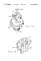
- FIG. 1is a prior-art molded leadframe pressure sensor package 1 .
- the sensor package 1includes a sensor die 2 that is attached to a housing 3 by a soft adhesive (e.g., RTV, epoxy, etc.), as shown by numeral 4 .
- the sensor package housing 3is generally made out of a pre-molded plastic and includes a metal leadframe 5 for providing interconnection to external circuitry.
- the topside 11 of the pressure sensoris typically coated with a silicone gel 6 for communicating pressure from external gaseous media.
- the packagefurther includes a lid 7 having an opening 8 for directing external pressure to the sensor.
- the silicone gel 6provides a minimal amount of protection from gaseous media for the sensor, wire interconnects, etc.
- pressureis applied from the topside 11
- a pressure port 10is provided on the bottom side 12 .
- this sensor package 1has several drawbacks.
- Third, the only use of fluid media with the sensorincludes exposure to the fluid media from the bottom side 12 of the sensor. However, adhesives, soft or hard, are not considered hermetic and, over time, moisture and corrosive gases will penetrate the interface, causing the electronics of the pressure sensor to fail.
- FIG. 2is a typical prior art sensor package 20 for high pressure and fluid media compatibility.
- This type of sensor package 20includes a sensor die 21 which is placed in a stainless steel housing 22 with hermetic glass feed-through pins 23 .
- the sensor die 21has an integral glass or silicon constraint bottom 24 which provides a sealing cavity 25 therebetween for a vacuum reference and stress isolation from the housing.
- the die attach materialis typically a soft epoxy such as RTV.
- a metal diaphragm 26is welded to the stainless steel housing 22 and an inside cavity 27 formed therein is filled with oil to allow transfer of pressure to the sensor die 21 .
- This configurationisolates the sensor die 21 from the fluid media.
- the use of the metal diaphragmis the primary packaging technique available today for more demanding applications, with variations in pressure and ability to apply most fluids to the sensor package. However, this type of package only generally addresses specific applications and is very expensive.
- the present inventionis a hermetic media interface for a sensor package.
- the hermetic media interfaceis incorporated into a pressure sensor package for interfacing directly to fluid and/or gaseous media.
- the pressure sensor packageincludes a semiconductor die and a pressure port that are housed in a pre-molded plastic package.
- a eutectic solderis coupled between the semiconductor die and a metal pressure port to solder the same to the semiconductor die.
- the semiconductor diemay be optionally metallized.
- the pressure portis made from one or more plastic materials and the pressure port is attached to the semiconductor die with an adhesive.
- An integral stress-isolation regionmay be optionally incorporated on the semiconductor die.
- FIG. 1is a prior-art molded leadframe pressure sensor package.
- FIG. 2is a typical prior-art sensor package for high pressure and media compatibility.
- FIGS. 3 a and 3 billustrate cut-away top and bottom views of a silicon pressure sensor package according to one embodiment of the present invention.
- FIG. 4illustrates a cross-sectional view of the silicon pressure sensor package of FIG. 3 where the pressure sensor die is also over-coated.
- FIG. 5 ais a schematic cross section of the sensor die bonded to the silicon cap according to one embodiment of the present invention.
- FIG. 5 bis a schematic cross-sectional view of a portion of the sensor die and silicon cap of FIG. 5 a , taken on an expanded scale.
- FIGS. 6 a through 6 eillustrate a triple boss diaphragm configuration according to another embodiment of the present invention.
- FIGS. 7 a and 7 billustrate the silicon pressure sensor of FIGS. 3 and 4 hermetically attached to a metal pressure port having a threaded pipe fitting and a hex outline, according to another embodiment of the present invention.
- the present inventionis a hermetic media interface for a sensor package.
- the hermetic media interfaceis incorporated into a pressure sensor package for interfacing directly to fluid and/or gaseous media.
- the pressure sensor packageallows fluid media (e.g., water, gasoline, saline, etc.) and/or gaseous media to be applied directly to the back of the pressure sensor die without incurring pressure leaks as a result of the hermetic media interface.
- FIGS. 3 a and 3 billustrate cut-away top and bottom views of a silicon pressure sensor package 100 according to one embodiment of the present invention.
- FIG. 4illustrates a cross-sectional view of the silicon pressure sensor package of FIG. 3 where the pressure sensor die is also over-coated.
- the silicon pressure sensor package 100has a top side 102 , housing the electronics of the pressure sensor, and a bottom side 104 which is exposed to the pressure media (e.g., gaseous, fluid, etc.).
- the pressure sensor package 100comprises a molded plastic housing 106 which embodies a metal insert 108 (hereinafter referred to as a “pressure port”). Alternatively, the pressure port 108 is molded into the plastic housing 106 .
- the housing 106is made from liquid crystal polymer (“LCP”) plastic materials.
- the pressure port 108is made from Invar 36 , kovar, brass or a combination of such materials.
- the pressure port 108is plated with electroless nickel, and optionally gold, for providing corrosion resistance and solderability.
- the pressure port 108may be made from plastic material(s).
- the silicon pressure sensor package 100further comprises a sensor die 110 that includes a diaphragm 112 .
- a plurality of piezoresistive elements(see, e.g., FIG. 6 d ) is disposed on the diaphragm 112 for sensing external pressure.
- the pressure port 108provides a hermetic path for fluids to a backside 115 of the sensor die 110 .
- a preform solder washer 114(ring), is provided for soldering and hermetically attaching the sensor die 110 directly to the pressure port 108 .
- the preform solder washer 114contains a combination of tin and silver, and preferably 96.5% tin and 3.5% silver having a eutectic melting point of 210° C.
- the preform solder washer 114contains a combination of gold and tin, and preferably 80% gold and 20% tin having a eutectic reflow temperature of 280° C.
- the pressure port 108is made from plastic material(s)
- the pressure port 108is attached to the sensor die 110 by an adhesive such as, but not limited or restricted to, RTV, epoxy, etc.
- the backside 115 of the sensor die 110may optionally be metallized with chromium and platinum for enhancing solderability and providing protection against exposure to fluids.
- the molded plastic housing 106also embodies a metal leadframe 116 for externally interconnecting the circuitry contained within the silicon pressure sensor package 100 .
- the metal leadframe 116may optionally be made from Alloy 42 , and optionally plated with electroless nickel and gold.
- the sensor die 110is bonded to a silicon cap 118 having a recess that forms a cavity 120 therebetween for allowing the diaphragm 112 to deflect responsive to applied pressure, and for providing a vacuum pressure reference.
- the silicon cap 118may be optionally bonded to active electronic circuitry 122 (e.g., an application specific integrated circuit “ASIC”) for providing amplification and signal correction.
- ASICapplication specific integrated circuit
- An exemplary active electronic circuitryincludes electronically trimmable circuitry which negates the need for laser trimming.
- the active electronic circuitry 122includes one or more pads 126 for connecting the active electronic circuitry to the leadframe 116 .
- a conformal coating 124e.g., RTV material 6611 , epoxy, parylene, etc.
- the silicon pressure sensor package 100is capable of withstanding high pressures and is extremely reliable due to its hermeticity. Therefore, there is very little risk of fluid contamination to the electronic side and the wire bond areas of the sensor package.
- FIG. 5 ais a schematic cross section of the sensor die 110 bonded to the silicon cap 118 according to one embodiment of the present invention.
- the sensor die 110includes the diaphragm 112 and an integral stress isolation flexible region 130 .
- the stress isolation region 130protects and isolates the diaphragm 112 from thermal and mounting stresses in the peripheral (or frame) region 132 of the sensor die 110 .
- the flexible diaphragm 112includes piezoresistive elements (See FIG. 6 d ) for sensing bending stresses from pressure applied to the diaphragm 112 .
- a bond ring 134is used to hermetically attach the cap 118 to the sensor die 110 and form a vacuum cavity 120 therebetween for providing an absolute pressure reference.
- the bond ring 134comprising aluminum, gold, or polysilicon, may be formed on the sensor die 110 , while the silicon cap 118 may be coated with germanium, uncoated, or gold coated, respectively.
- the bondis formed at the wafer level by placing the two wafers in physical contact under elevated temperature and pressure.
- FIG. 5 bis a schematic cross-sectional view of a portion of the sensor die 110 and silicon cap 118 of FIG. 5 a , taken on an expanded scale.
- the stress isolation flexible region 130includes a horizontal member 140 integral with the frame region 132 , and a vertical member 142 having a first end integral with a second end of the horizontal member 140 , and a second end integral with a rim region 144 .
- an oxide layer 146is formed on the silicon substrate sensor die 110 using, for example, a Silicon Implanted with Oxygen (“SIMOX”) or Bonded and Etched Silicon-on-Insulator (“BESOI”) technique commonly known in the art.
- SIMOXSilicon Implanted with Oxygen
- BESOIBonded and Etched Silicon-on-Insulator
- the oxide layer 146provides a suitable etch stop for a bottom side etch.
- a silicon epitaxial layer 148(e.g., N-) is then deposited, as needed, above the oxide layer 146 to increase the thickness of the diaphragm 112 .
- Moderately doped P-type layers 150 and 152are formed in the epitaxial layer 148 .
- a second oxide layer 154is disposed over the epitaxial layer 148 extending across the width of the sensor die 110 .
- the upper trench 156is formed, as will be described in more detail below.
- the second oxide layer 154is etched in at least three places including an etch on the outside of the bond ring 134 , as shown by numeral 159 , and at both sides of the stress isolation region 130 , as shown by numerals 160 and 162 .
- a pad 136is placed over the etch 159 outside of the bond ring 134 , and a metal interconnect layer 164 is placed between etches 160 and 162 .
- the doped P-type layer 150connects the metal interconnect layer 164 at numeral 160 , under the bond ring 134 , to the pad 136 .
- the doped P-type layer 152connects the metal interconnect layer 164 at numeral 162 to circuitry in the diaphragm region 112 such as a piezoresistive element (See FIG. 6 d ). This provides interconnection between the piezoresistive elements disposed on the diaphragm 112 (and other circuitry inside the bond ring 134 ) and one or more pads 136 outside of the bond ring 134 .
- the second oxide layer 154also isolates the P-type layer 150 from the eutectic bond ring 134 .
- the horizontal and vertical members 140 and 142are formed by vertically etching upper and lower trenches 156 and 158 from the top and the bottom of the sensor die 110 , respectively. A series of silicon and oxide etch steps are utilized to complete the upper trench 156 . Formation of the horizontal and vertical members 140 and 142 is achieved using an etching process such as, but not limited or restricted to, deep reactive ion etching (“D-RIE”) of silicon, a known etching technique which allows deep trenches to be etched in silicon with high aspect ratios and nearly vertical walls on each side of the wafer.
- D-RIEdeep reactive ion etching
- the pressure-sensitive diaphragm 112can also be etched using the D-RIE technique, and may be done at the same time as the backside etch used to form the horizontal member 140 .
- Accuracy in the thickness of the horizontal member 140 and deformable diaphragm 112is enhanced by the inclusion of the oxide layer 146 at a depth from the top surface equal to the desired thickness of the diaphragm, since the etch rate of such oxide is much slower than that of bulk silicon.
- silicon-on-insulator (“SOI”) materialis used in cases where a thin, highly uniform diaphragm 112 is desired, standard material (non-SOI) may be used in conjunction with a timed etch to provide a thicker diaphragm.
- Electric discharge machining or other micromachining techniquesmay also be used to form the flexible horizontal and vertical members 140 and 142 , if desired.
- the horizontal and vertical members 140 and 142each have an aspect ratio (length to thickness) of approximately 10 to 1. That is, the length of each member is approximately ten times the thickness of the respective member, thereby providing good flexibility to confine externally generated stresses to the frame region 132 only. Other aspect ratios, as low as 1:1 or greater than 10:1, may be used depending on a number of factors including, but not limited to, the amount of stress that the frame region 132 may be subjected to, the thickness of the diaphragm 112 , etc.
- the stress isolation flexible region 130 so formedis integral with the outer frame region 132 .
- the horizontal and vertical members 140 and 142support a nominally rigid rim region 144 with the same providing an isolated, rigid support for the pressure-sensitive diaphragm 112 .
- FIG. 6 aa cross-sectional view of a triple boss diaphragm configuration of the sensor die 110 may be seen.
- Thisis an alternative embodiment of the diaphragm 112 shown in FIGS. 4, 5 a , and 5 b .
- the diaphragm 112is formed in the silicon sensor die 110 and is structurally supported at its periphery 170 .
- the diaphragm 112is exposed to applied pressure on one or both sides (e.g., P 1 and/or P 0 ).
- the diaphragm 112is substantially planar and includes three nominally rigid members 172 (hereinafter referred to as “bosses”) of increased thickness arrayed across the midsection or axis of the pressure sensor (see, e.g., FIG. 6 d ).
- the bosses 172are equally spaced apart from the periphery 170 and each other. However, this is not a requirement as the bosses 172 may be spaced apart in unequal increments.
- the regions 174 between the bosses 172 and between a boss 172 and the periphery 170have a smaller thickness than the thickness of the bosses 172 and are hereinafter referred to as “thinner regions”.
- the bosses 172locally stiffen the diaphragm 112 and focus the bending stresses on the thinner regions 174 .
- FIG. 6 billustrates the displacement profile of the triple boss diaphragm configuration of FIG. 6 a .
- FIG. 6 cillustrates the stress profile along the upper surface of the diaphragm. The stress profile is associated with the bending profile of FIG. 6 b .
- high tensile stresses 176are found in the thinner regions 174 between the bosses 172 and high compressive stresses 178 are found in the thinner regions next to the diaphragm periphery 170 . It is these thinner regions 174 where the piezoresistive elements are selectively positioned, as shown in FIG. 6 d.
- FIG. 6 dillustrates a backside view of the triple boss diaphragm configuration.
- four piezoresistive elements 180are shown for clarity purposes only, as they are actually disposed on the topside of the diaphragm 112 .
- two of the piezoresistive elementsare located in the thinner regions of tensile stress (between the bosses 172 ) and the other two are located in the thinner regions of compressive stress (between a boss 172 and periphery 170 ).
- the piezoresistive elementsare formed in the middle of the thinner regions. This balances any effects of stress from the bosses 172 .
- the piezoresistive elements 180are connected in a Wheatstone bridge configuration (not shown).
- the piezoresistive elements 180are all similarly aligned, i.e., they are either all parallel to the diaphragm edges 170 (as depicted) or all perpendicular to the diaphragm edges 170 .
- a bias voltageis applied to the Wheatstone bridge. Orienting the piezoresistive elements 180 in the same direction cancels out common-mode stress effects due to packaging and mounting stresses while still providing high sensitivity. Axial stresses (horizontal and/or vertical) from packaging and temperature effects vary the resistance values of the four piezoresistive elements in the same way, thereby canceling such unwanted effects.
- a pressure differential across the diaphragm 112causes the resistances of the two piezoresistive elements in opposite legs of the Wheatstone bridge to increase, and the resistances of the other two piezoresistive elements to decrease, resulting in a differential output voltage of the Wheatstone bridge which is a direct measure of the applied pressure.
- FIG. 6 eillustrates a cross-sectional view of a single boss, according to the embodiment of FIG. 6 a .
- the diaphragm 112(a portion of which is shown) is formed by first incorporating an oxide layer 182 on the substrate 110 , disposing a silicon layer 184 on the oxide layer 182 by a wafer bonding and etch-back technique, and masking and etching the back side 186 of the substrate 110 to form the diaphragm 112 .
- the buried oxide layer 182acts as an automatic etch stop to provide uniformity in the depth of the etch.
- the substrate 110is etched from the back side 186 using the D-RIE technique to form substantially vertical sidewalls of the bosses 172 .
- the area of the diaphragmmay be decreased and/or its thickness may be increased.
- An epitaxial silicon layerfor example, may be deposited on the silicon layer 184 to achieve this additional thickness.
- the etch stop oxide layer 182may not be required.
- the triple boss configurationprovides improved pressure non-linearity with a large output signal in response to applied pressure, while providing a higher degree of common-mode cancellation of detrimental effects due to temperature, package induced stresses, and mounting stresses. Furthermore, the multiple boss configuration (e.g., three bosses) focuses the stress between the bosses to provide stress amplification therebetween, produces identical “in-board” and “outboard” stresses except for sign, and provides high curvature in the thinner regions 174 between the bosses and between a boss and the periphery with low curvature in the boss and rim regions.
- FIGS. 7 a and 7 billustrates the silicon pressure sensor of FIGS. 3 and 4 hermetically attached to a metal pressure port 190 having a threaded pipe fitting 192 and a hex outline 194 , according to another embodiment of the present invention.
- the pre-molded plastic package 196has a metal insert ring 198 for aligning the silicon die 200 with the pressure port 190 during the die attach process, and mounting the pre-molded package to the metal port 190 via solder. This style of packaging allows for easy and flexible design changes to the pressure port independent of the tooling and assembly flow.
- the present inventionuses solder to attach the sensor element onto a metal pressure port in a low cost plastic packaging technology.
- the solder die attachprovides a long term reliable solution for a hermetic pressure seal to the backside of the silicon sensor die.
Landscapes
- Physics & Mathematics (AREA)
- General Physics & Mathematics (AREA)
- Chemical & Material Sciences (AREA)
- Analytical Chemistry (AREA)
- Measuring Fluid Pressure (AREA)
- Pressure Sensors (AREA)
Abstract
Description
1. Field of the Invention
The present invention relates generally to semiconductor pressure sensors, and specifically, to hermetic packaging of semiconductor pressure sensors.
2. Background Information
Today, most low-cost pressure sensor packages are designed to address clean gases and/or non-aggressive fluids. FIG. 1 is a prior-art molded leadframe pressure sensor package1. The sensor package1 includes asensor die 2 that is attached to a housing3 by a soft adhesive (e.g., RTV, epoxy, etc.), as shown by numeral4. The sensor package housing3 is generally made out of a pre-molded plastic and includes ametal leadframe 5 for providing interconnection to external circuitry. The topside11 of the pressure sensor is typically coated with asilicone gel 6 for communicating pressure from external gaseous media. The package further includes a lid7 having anopening 8 for directing external pressure to the sensor. Thesilicone gel 6 provides a minimal amount of protection from gaseous media for the sensor, wire interconnects, etc. In the case of an absolute pressure sensor, pressure is applied from the topside11, whereas for gage or differential pressure sensing, apressure port 10 is provided on thebottom side 12.
However, this sensor package1 has several drawbacks. First, since thesensor die 2 is attached to the housing3 with a soft die attach material, the applied pressures from thebottom side 12 of the sensor die is typically limited to less than 150 pounds per square inch (“psi”). Second, the topside11 of the sensor only supports inert gaseous with pressures limited again to less than 150 psi. This is because the pressure media that is applied to the topside11 of the sensor will penetrate the intermediary coating (e.g., the silicone gel or other type of coating), causing reliability issues such as failure of the sensor over time or explosion of the silicone gel after rapid pressure changes. Third, the only use of fluid media with the sensor includes exposure to the fluid media from thebottom side 12 of the sensor. However, adhesives, soft or hard, are not considered hermetic and, over time, moisture and corrosive gases will penetrate the interface, causing the electronics of the pressure sensor to fail.
FIG. 2 is a typical priorart sensor package 20 for high pressure and fluid media compatibility. This type ofsensor package 20 includes asensor die 21 which is placed in astainless steel housing 22 with hermetic glass feed-through pins 23. Thesensor die 21 has an integral glass orsilicon constraint bottom 24 which provides asealing cavity 25 therebetween for a vacuum reference and stress isolation from the housing. The die attach material is typically a soft epoxy such as RTV. Ametal diaphragm 26 is welded to thestainless steel housing 22 and aninside cavity 27 formed therein is filled with oil to allow transfer of pressure to the sensor die21. This configuration isolates the sensor die21 from the fluid media. The use of the metal diaphragm is the primary packaging technique available today for more demanding applications, with variations in pressure and ability to apply most fluids to the sensor package. However, this type of package only generally addresses specific applications and is very expensive.
Accordingly, there is a long-felt need in the sensor industry for a low-cost, long-term reliable solution to address the problems associated with conventional pressure sensors.
The present invention is a hermetic media interface for a sensor package. The hermetic media interface is incorporated into a pressure sensor package for interfacing directly to fluid and/or gaseous media. The pressure sensor package includes a semiconductor die and a pressure port that are housed in a pre-molded plastic package. In one embodiment, a eutectic solder is coupled between the semiconductor die and a metal pressure port to solder the same to the semiconductor die. The semiconductor die may be optionally metallized. In an alternative embodiment, the pressure port is made from one or more plastic materials and the pressure port is attached to the semiconductor die with an adhesive. An integral stress-isolation region may be optionally incorporated on the semiconductor die.
FIG. 1 is a prior-art molded leadframe pressure sensor package.
FIG. 2 is a typical prior-art sensor package for high pressure and media compatibility.
FIGS. 3aand3billustrate cut-away top and bottom views of a silicon pressure sensor package according to one embodiment of the present invention.
FIG. 4 illustrates a cross-sectional view of the silicon pressure sensor package of FIG. 3 where the pressure sensor die is also over-coated.
FIG. 5ais a schematic cross section of the sensor die bonded to the silicon cap according to one embodiment of the present invention.
FIG. 5bis a schematic cross-sectional view of a portion of the sensor die and silicon cap of FIG. 5a, taken on an expanded scale.
FIGS. 6athrough6eillustrate a triple boss diaphragm configuration according to another embodiment of the present invention.
FIGS. 7aand7billustrate the silicon pressure sensor of FIGS. 3 and 4 hermetically attached to a metal pressure port having a threaded pipe fitting and a hex outline, according to another embodiment of the present invention.
The present invention is a hermetic media interface for a sensor package. In one embodiment, the hermetic media interface is incorporated into a pressure sensor package for interfacing directly to fluid and/or gaseous media. The pressure sensor package allows fluid media (e.g., water, gasoline, saline, etc.) and/or gaseous media to be applied directly to the back of the pressure sensor die without incurring pressure leaks as a result of the hermetic media interface.
FIGS. 3aand3billustrate cut-away top and bottom views of a siliconpressure sensor package 100 according to one embodiment of the present invention. FIG. 4 illustrates a cross-sectional view of the silicon pressure sensor package of FIG. 3 where the pressure sensor die is also over-coated. Referring to FIGS. 3 and 4, the siliconpressure sensor package 100 has atop side 102, housing the electronics of the pressure sensor, and abottom side 104 which is exposed to the pressure media (e.g., gaseous, fluid, etc.). Thepressure sensor package 100 comprises a moldedplastic housing 106 which embodies a metal insert108 (hereinafter referred to as a “pressure port”). Alternatively, thepressure port 108 is molded into theplastic housing 106. This allows thepressure port 108 to be configured into different shapes and sizes to maintain compatibility with different interfaces. In one embodiment, thehousing 106 is made from liquid crystal polymer (“LCP”) plastic materials. Moreover, thepressure port 108 is made from Invar36, kovar, brass or a combination of such materials. Thepressure port 108 is plated with electroless nickel, and optionally gold, for providing corrosion resistance and solderability. Alternatively, thepressure port 108 may be made from plastic material(s).
The siliconpressure sensor package 100 further comprises a sensor die110 that includes adiaphragm 112. A plurality of piezoresistive elements (see, e.g., FIG. 6d) is disposed on thediaphragm 112 for sensing external pressure. Thepressure port 108 provides a hermetic path for fluids to abackside 115 of the sensor die110. A preform solder washer114 (ring), is provided for soldering and hermetically attaching the sensor die110 directly to thepressure port 108. In one embodiment, thepreform solder washer 114 contains a combination of tin and silver, and preferably 96.5% tin and 3.5% silver having a eutectic melting point of 210° C. In another embodiment, thepreform solder washer 114 contains a combination of gold and tin, and preferably 80% gold and 20% tin having a eutectic reflow temperature of 280° C. In the case where thepressure port 108 is made from plastic material(s), thepressure port 108 is attached to the sensor die110 by an adhesive such as, but not limited or restricted to, RTV, epoxy, etc.
Thebackside 115 of the sensor die110 may optionally be metallized with chromium and platinum for enhancing solderability and providing protection against exposure to fluids. The moldedplastic housing 106 also embodies ametal leadframe 116 for externally interconnecting the circuitry contained within the siliconpressure sensor package 100. Themetal leadframe 116 may optionally be made from Alloy42, and optionally plated with electroless nickel and gold.
The sensor die110 is bonded to asilicon cap 118 having a recess that forms acavity 120 therebetween for allowing thediaphragm 112 to deflect responsive to applied pressure, and for providing a vacuum pressure reference. Thesilicon cap 118 may be optionally bonded to active electronic circuitry122 (e.g., an application specific integrated circuit “ASIC”) for providing amplification and signal correction. An exemplary active electronic circuitry includes electronically trimmable circuitry which negates the need for laser trimming. As shown in FIG. 3a, the activeelectronic circuitry 122 includes one ormore pads 126 for connecting the active electronic circuitry to theleadframe 116. A conformal coating124 (e.g., RTV material6611, epoxy, parylene, etc.) is applied to thetopside 102 of the sensor for completing the sensor package and protecting the electronics contained therein.
The siliconpressure sensor package 100 is capable of withstanding high pressures and is extremely reliable due to its hermeticity. Therefore, there is very little risk of fluid contamination to the electronic side and the wire bond areas of the sensor package.
FIG. 5ais a schematic cross section of the sensor die110 bonded to thesilicon cap 118 according to one embodiment of the present invention. As shown in FIG. 5a, the sensor die110 includes thediaphragm 112 and an integral stress isolationflexible region 130. Thestress isolation region 130 protects and isolates thediaphragm 112 from thermal and mounting stresses in the peripheral (or frame)region 132 of the sensor die110. Theflexible diaphragm 112 includes piezoresistive elements (See FIG. 6d) for sensing bending stresses from pressure applied to thediaphragm 112. Abond ring 134 is used to hermetically attach thecap 118 to the sensor die110 and form avacuum cavity 120 therebetween for providing an absolute pressure reference. By way of illustration, thebond ring 134, comprising aluminum, gold, or polysilicon, may be formed on the sensor die110, while thesilicon cap 118 may be coated with germanium, uncoated, or gold coated, respectively. The bond is formed at the wafer level by placing the two wafers in physical contact under elevated temperature and pressure.
FIG. 5bis a schematic cross-sectional view of a portion of the sensor die110 andsilicon cap 118 of FIG. 5a, taken on an expanded scale. As shown in FIG. 5b, the stress isolationflexible region 130 includes ahorizontal member 140 integral with theframe region 132, and avertical member 142 having a first end integral with a second end of thehorizontal member 140, and a second end integral with arim region 144. Prior to formation of the horizontal andvertical members diaphragm 112, an oxide layer146 is formed on the silicon substrate sensor die110 using, for example, a Silicon Implanted with Oxygen (“SIMOX”) or Bonded and Etched Silicon-on-Insulator (“BESOI”) technique commonly known in the art. The oxide layer146 provides a suitable etch stop for a bottom side etch. A silicon epitaxial layer148 (e.g., N-) is then deposited, as needed, above the oxide layer146 to increase the thickness of thediaphragm 112. Moderately doped P-type layers epitaxial layer 148.
Asecond oxide layer 154 is disposed over theepitaxial layer 148 extending across the width of the sensor die110. After depositing thesecond oxide layer 154, theupper trench 156 is formed, as will be described in more detail below. Thesecond oxide layer 154 is etched in at least three places including an etch on the outside of thebond ring 134, as shown bynumeral 159, and at both sides of thestress isolation region 130, as shown bynumerals pad 136 is placed over theetch 159 outside of thebond ring 134, and ametal interconnect layer 164 is placed betweenetches type layer 150 connects themetal interconnect layer 164 atnumeral 160, under thebond ring 134, to thepad 136. The doped P-type layer 152 connects themetal interconnect layer 164 at numeral162 to circuitry in thediaphragm region 112 such as a piezoresistive element (See FIG. 6d). This provides interconnection between the piezoresistive elements disposed on the diaphragm112 (and other circuitry inside the bond ring134) and one ormore pads 136 outside of thebond ring 134. Thesecond oxide layer 154 also isolates the P-type layer 150 from theeutectic bond ring 134.
The horizontal andvertical members lower trenches upper trench 156. Formation of the horizontal andvertical members sensitive diaphragm 112 can also be etched using the D-RIE technique, and may be done at the same time as the backside etch used to form thehorizontal member 140.
Accuracy in the thickness of thehorizontal member 140 anddeformable diaphragm 112 is enhanced by the inclusion of the oxide layer146 at a depth from the top surface equal to the desired thickness of the diaphragm, since the etch rate of such oxide is much slower than that of bulk silicon. Though silicon-on-insulator (“SOI”) material is used in cases where a thin, highlyuniform diaphragm 112 is desired, standard material (non-SOI) may be used in conjunction with a timed etch to provide a thicker diaphragm. Electric discharge machining or other micromachining techniques may also be used to form the flexible horizontal andvertical members
In one embodiment, the horizontal andvertical members frame region 132 only. Other aspect ratios, as low as 1:1 or greater than 10:1, may be used depending on a number of factors including, but not limited to, the amount of stress that theframe region 132 may be subjected to, the thickness of thediaphragm 112, etc. The stress isolationflexible region 130 so formed is integral with theouter frame region 132. The horizontal andvertical members rigid rim region 144 with the same providing an isolated, rigid support for the pressure-sensitive diaphragm 112.
Referring now to FIG. 6a, a cross-sectional view of a triple boss diaphragm configuration of the sensor die110 may be seen. This is an alternative embodiment of thediaphragm 112 shown in FIGS. 4,5a, and5b. In this embodiment, thediaphragm 112 is formed in the silicon sensor die110 and is structurally supported at itsperiphery 170. Thediaphragm 112 is exposed to applied pressure on one or both sides (e.g., P1 and/or P0). Thediaphragm 112 is substantially planar and includes three nominally rigid members172 (hereinafter referred to as “bosses”) of increased thickness arrayed across the midsection or axis of the pressure sensor (see, e.g., FIG. 6d).
In the embodiment shown, thebosses 172 are equally spaced apart from theperiphery 170 and each other. However, this is not a requirement as thebosses 172 may be spaced apart in unequal increments. Theregions 174 between thebosses 172 and between aboss 172 and theperiphery 170 have a smaller thickness than the thickness of thebosses 172 and are hereinafter referred to as “thinner regions”. Thebosses 172 locally stiffen thediaphragm 112 and focus the bending stresses on thethinner regions 174.
FIG. 6billustrates the displacement profile of the triple boss diaphragm configuration of FIG. 6a. Although this figure is greatly exaggerated, the amount of diaphragm bending is much higher in thethinner regions 174 than the negligible bending in the regions stiffened by thebosses 172. FIG. 6cillustrates the stress profile along the upper surface of the diaphragm. The stress profile is associated with the bending profile of FIG. 6b. As shown in FIG. 6c, hightensile stresses 176 are found in thethinner regions 174 between thebosses 172 and high compressive stresses178 are found in the thinner regions next to thediaphragm periphery 170. It is thesethinner regions 174 where the piezoresistive elements are selectively positioned, as shown in FIG. 6d.
FIG. 6dillustrates a backside view of the triple boss diaphragm configuration. In this view, fourpiezoresistive elements 180 are shown for clarity purposes only, as they are actually disposed on the topside of thediaphragm 112. In the embodiment being described, two of the piezoresistive elements are located in the thinner regions of tensile stress (between the bosses172) and the other two are located in the thinner regions of compressive stress (between aboss 172 and periphery170). In one embodiment, the piezoresistive elements are formed in the middle of the thinner regions. This balances any effects of stress from thebosses 172. Thepiezoresistive elements 180 are connected in a Wheatstone bridge configuration (not shown).
Note that thepiezoresistive elements 180 are all similarly aligned, i.e., they are either all parallel to the diaphragm edges170 (as depicted) or all perpendicular to the diaphragm edges170. In operation, a bias voltage is applied to the Wheatstone bridge. Orienting thepiezoresistive elements 180 in the same direction cancels out common-mode stress effects due to packaging and mounting stresses while still providing high sensitivity. Axial stresses (horizontal and/or vertical) from packaging and temperature effects vary the resistance values of the four piezoresistive elements in the same way, thereby canceling such unwanted effects. A pressure differential across thediaphragm 112 causes the resistances of the two piezoresistive elements in opposite legs of the Wheatstone bridge to increase, and the resistances of the other two piezoresistive elements to decrease, resulting in a differential output voltage of the Wheatstone bridge which is a direct measure of the applied pressure.
FIG. 6eillustrates a cross-sectional view of a single boss, according to the embodiment of FIG. 6a. Referring to FIG. 6e, the diaphragm112 (a portion of which is shown) is formed by first incorporating anoxide layer 182 on thesubstrate 110, disposing a silicon layer184 on theoxide layer 182 by a wafer bonding and etch-back technique, and masking and etching theback side 186 of thesubstrate 110 to form thediaphragm 112. The buriedoxide layer 182 acts as an automatic etch stop to provide uniformity in the depth of the etch. In a preferred embodiment, thesubstrate 110 is etched from theback side 186 using the D-RIE technique to form substantially vertical sidewalls of thebosses 172. For high-pressure designs, the area of the diaphragm may be decreased and/or its thickness may be increased. An epitaxial silicon layer, for example, may be deposited on the silicon layer184 to achieve this additional thickness. For higher-pressure ranges, where thediaphragm 112 is thicker, the etchstop oxide layer 182 may not be required.
The triple boss configuration provides improved pressure non-linearity with a large output signal in response to applied pressure, while providing a higher degree of common-mode cancellation of detrimental effects due to temperature, package induced stresses, and mounting stresses. Furthermore, the multiple boss configuration (e.g., three bosses) focuses the stress between the bosses to provide stress amplification therebetween, produces identical “in-board” and “outboard” stresses except for sign, and provides high curvature in thethinner regions 174 between the bosses and between a boss and the periphery with low curvature in the boss and rim regions.
FIGS. 7aand7billustrates the silicon pressure sensor of FIGS. 3 and 4 hermetically attached to ametal pressure port 190 having a threaded pipe fitting192 and ahex outline 194, according to another embodiment of the present invention. The pre-moldedplastic package 196 has ametal insert ring 198 for aligning the silicon die200 with thepressure port 190 during the die attach process, and mounting the pre-molded package to themetal port 190 via solder. This style of packaging allows for easy and flexible design changes to the pressure port independent of the tooling and assembly flow.
The present invention uses solder to attach the sensor element onto a metal pressure port in a low cost plastic packaging technology. In one embodiment, it is desirable to have the sensor die attached to the metal insert using non-organic die attach materials, such as solder, to provide better hermeticity and heat transfer, higher working temperature, etc. In the case of sensor packaging, the solder die attach provides a long term reliable solution for a hermetic pressure seal to the backside of the silicon sensor die.
While certain exemplary embodiments have been described and shown in the accompanying drawings, it is to be understood that such embodiments are merely illustrative of and not restrictive on the broad invention, and that this invention not be limited to the specific constructions and arrangements shown and described, since various other modifications may occur to those ordinarily skilled in the art.
Claims (37)
1. A hermetic media interface for a sensor package, comprising:
a semiconductor die;
a metal pressure port; and
a eutectic solder coupled between the semiconductor die and the metal pressure port.
2. The hermetic media interface ofclaim 1 , wherein the metal pressure port and the semiconductor die are housed in a pre-molded plastic package.
3. The hermetic media interface ofclaim 1 , wherein a backside of the semiconductor die is metallized.
4. The hermetic media interface ofclaim 1 , wherein a backside of the semiconductor die is metallized with chromium and platinum.
5. The hermetic media interface ofclaim 1 , wherein the metal pressure port is made from one or more of the following: Invar, kovar, and brass.
6. The hermetic media interface ofclaim 1 , wherein the metal pressure port is plated with one or more of the following: electroless nickel and gold.
7. The hermetic media interface ofclaim 1 , wherein the eutectic solder includes gold and tin.
8. The hermetic media interface ofclaim 1 , wherein the eutectic solder is made from 80% gold and 20% tin.
9. The hermetic media interface ofclaim 1 , wherein the eutectic solder is made from 96.5% tin and 3.5% silver.
10. The hermetic media interface ofclaim 1 , wherein the solder is applied in a paste form.
11. The hermetic media interface ofclaim 1 , wherein the semiconductor die includes a deformable diaphragm and a frame region that surrounds the deformable diaphragm.
12. The hermetic media interface ofclaim 11 , wherein the deformable diaphragm includes piezoresistors disposed thereon for sensing pressure.
13. The hermetic media interface ofclaim 11 , wherein the semiconductor die incorporates a stress isolation flexible region between the frame region and the deformable diaphragm.
14. The hermetic media interface ofclaim 11 , further comprising a cap having a recess, the cap being attached to the semiconductor die to form a cavity therebetween for allowing deflection of the deformable diaphragm.
15. The hermetic media interface ofclaim 14 , wherein the cap is made from silicon.
16. The hermetic media interface ofclaim 14 , wherein the cap further includes a second pressure port for providing a differential measurement.
17. The hermetic media interface ofclaim 2 , wherein the metal pressure port is insert molded or inserted subsequent to the molding of the pre-molded package.
18. The hermetic media interface ofclaim 2 , wherein the semiconductor die is attached to the metal pressure port independent of molding of the pre-molded plastic package.
19. The hermetic media interface ofclaim 1 , wherein the solder is applied to the metal pressure port prior to the semiconductor die being reflowed to the metal pressure port.
20. A sensor system having a hermetic media interface, comprising:
a semiconductor die;
a metal pressure port;
a pre-molded plastic package containing the semiconductor die; and
a ring coupled between the metal pressure port and the semiconductor die to attach the same with the metal pressure port.
21. The system ofclaim 20 , wherein the ring is a eutectic solder to solder the semiconductor die to the metal pressure port.
22. The system ofclaim 20 , wherein the metal pressure port is made from one or more plastic materials, and the ring is a die-attach adhesive which includes one or more of the following: RTV and epoxy.
23. The system ofclaim 21 , wherein the semiconductor die is metallized with chromium and platinum on a solder side.
24. The system ofclaim 20 , wherein the metal pressure port is made from one or more of the following metals: Invar, kovar, and brass.
25. The system ofclaim 21 , wherein the metal pressure port is plated with one or more of the following: electroless nickel and gold.
26. The system ofclaim 21 , wherein the eutectic solder includes gold and tin.
27. The system ofclaim 21 , wherein the eutectic solder is made from 80% gold and 20% tin.
28. The system ofclaim 21 , wherein the eutectic solder is made from 96.5% tin and 3.5% silver.
29. The system ofclaim 20 , wherein the semiconductor die includes a diaphragm region and a frame region surrounding the diaphragm region, the diaphragm region having piezoresistive elements disposed thereon to sense pressure.
30. The system ofclaim 29 , wherein the semiconductor die incorporates an integral stress isolation region between the frame and diaphragm regions.
31. The system ofclaim 29 , wherein the semiconductor die is attached to a silicon cap having a cavity to allow the deflection of the diaphragm region.
32. The system ofclaim 31 , wherein the cap includes a second pressure port.
33. The system ofclaim 20 , wherein the metal pressure port is incorporated into a housing having a threaded pipe fitting.
34. The system ofclaim 33 , wherein the metal pressure port has features for crimping the housing to further protect the electronics.
35. A method of providing a hermetic media interface, comprising the combined acts of:
providing a semiconductor die;
metallizing a backside of the semiconductor die;
soldering the semiconductor die to a metal pressure port using a eutectic solder; and
housing the metal pressure port and semiconductor die in a pre-molded plastic package.
36. The method ofclaim 35 wherein soldering the semiconductor die comprises soldering the semiconductor die to the metal pressure port using the eutectic solder including a combination of tin and silver.
37. The method ofclaim 35 wherein soldering the semiconductor die comprises soldering the semiconductor die to the metal pressure port using the eutectic solder including a combination of gold and tin.
Priority Applications (2)
| Application Number | Priority Date | Filing Date | Title |
|---|---|---|---|
| US09/191,718US6351996B1 (en) | 1998-11-12 | 1998-11-12 | Hermetic packaging for semiconductor pressure sensors |
| PCT/US1999/024581WO2000029823A1 (en) | 1998-11-12 | 1999-10-20 | Hermetic packaging for semiconductor pressure sensors |
Applications Claiming Priority (1)
| Application Number | Priority Date | Filing Date | Title |
|---|---|---|---|
| US09/191,718US6351996B1 (en) | 1998-11-12 | 1998-11-12 | Hermetic packaging for semiconductor pressure sensors |
Publications (1)
| Publication Number | Publication Date |
|---|---|
| US6351996B1true US6351996B1 (en) | 2002-03-05 |
Family
ID=22706663
Family Applications (1)
| Application Number | Title | Priority Date | Filing Date |
|---|---|---|---|
| US09/191,718Expired - LifetimeUS6351996B1 (en) | 1998-11-12 | 1998-11-12 | Hermetic packaging for semiconductor pressure sensors |
Country Status (2)
| Country | Link |
|---|---|
| US (1) | US6351996B1 (en) |
| WO (1) | WO2000029823A1 (en) |
Cited By (86)
| Publication number | Priority date | Publication date | Assignee | Title |
|---|---|---|---|---|
| US20030167851A1 (en)* | 2002-01-30 | 2003-09-11 | Parker Gregory D. | Absolute micromachined silicon pressure sensor with backside hermetic cover and method of making the same |
| US6619129B2 (en)* | 2002-02-15 | 2003-09-16 | Delphi Technologies, Inc. | Three-piece pressure sensor with high pressure stainless steel sensing element |
| US20040200286A1 (en)* | 2002-06-22 | 2004-10-14 | Martin Mast | High pressure sensor comprising silicon membrane and solder layer |
| WO2004111595A1 (en)* | 2003-06-13 | 2004-12-23 | Telecom Italia S.P.A. | Pressure sensor with integrated structure |
| WO2005038422A1 (en) | 2003-10-01 | 2005-04-28 | General Electric Company | Surface mount package and method for forming multi-chip microsensor device |
| US7056765B2 (en) | 2002-11-15 | 2006-06-06 | Stmicroelectronics Asia Pacific Pte Ltd. | Semiconductor device package and method of manufacture |
| US20060164203A1 (en)* | 2002-06-22 | 2006-07-27 | Martin Mast | High-pressure sensor housing which is simplified by means of a connection element (also emc) |
| US20060196273A1 (en)* | 2004-12-12 | 2006-09-07 | Burns David W | Optically coupled resonator |
| US20060247539A1 (en)* | 2005-04-28 | 2006-11-02 | Schugt Michael A | Implantable capacitive pressure sensor system and method |
| US20060275143A1 (en)* | 2005-05-20 | 2006-12-07 | Copeland Corporation | Sensor for hermetic machine |
| US20070013014A1 (en)* | 2005-05-03 | 2007-01-18 | Shuwen Guo | High temperature resistant solid state pressure sensor |
| US7176048B1 (en) | 2004-12-12 | 2007-02-13 | Burns David W | Optically coupled sealed-cavity resonator and process |
| US20070069000A1 (en)* | 2005-09-27 | 2007-03-29 | Honeywell International Inc. | Method of flip chip mounting pressure sensor dies to substrates and pressure sensors formed thereby |
| US20070074577A1 (en)* | 2005-10-05 | 2007-04-05 | Honeywell International Inc. | Pressure sensor |
| US20070222009A1 (en)* | 2006-03-24 | 2007-09-27 | Infineon Technologies Sensonor As | Integrated Pedestal Mount for MEMS Structure |
| US7379629B1 (en) | 2004-12-12 | 2008-05-27 | Burns David W | Optically coupled resonant pressure sensor |
| US7443509B1 (en) | 2004-12-12 | 2008-10-28 | Burns David W | Optical and electronic interface for optically coupled resonators |
| US7499604B1 (en) | 2004-12-12 | 2009-03-03 | Burns David W | Optically coupled resonant pressure sensor and process |
| US20090060749A1 (en)* | 2007-08-28 | 2009-03-05 | Emerson Climate Technologies, Inc. | Molded Plug For A Compressor |
| US20090108382A1 (en)* | 2005-05-03 | 2009-04-30 | Odd Harald Steen Eriksen | Transducer for use in harsh environments |
| US20090139338A1 (en)* | 2007-09-28 | 2009-06-04 | James Tjan-Meng Suminto | Silicon sensing structure to detect through-plane motion in a plane of material with thermal expansion substantially different from that of silicon |
| US20090282925A1 (en)* | 2008-05-14 | 2009-11-19 | Honeywell International Inc. | Asic compensated pressure sensor with soldered sense die attach |
| US20100047491A1 (en)* | 2005-05-03 | 2010-02-25 | Rosemount Aerospace Inc. | Transient liquid phase eutectic bonding |
| US7726197B2 (en)* | 2006-04-26 | 2010-06-01 | Honeywell International Inc. | Force sensor package and method of forming same |
| US20110000318A1 (en)* | 2009-07-02 | 2011-01-06 | Honeywell International Inc. | Force sensor apparatus |
| US20110023618A1 (en)* | 2009-07-31 | 2011-02-03 | Temic Automotive Of North America, Inc. | Low pressure sensor device with high accuracy and high sensitivity |
| US20110031565A1 (en)* | 2009-08-04 | 2011-02-10 | David Lambe Marx | Micromachined devices and fabricating the same |
| US20110121413A1 (en)* | 2009-11-17 | 2011-05-26 | Howard Allen | Microelectromechanical systems microphone packaging systems |
| WO2011083158A3 (en)* | 2010-01-11 | 2011-11-10 | Elmos Semiconductor Ag | Micro-electromechanical semiconductor component |
| US20120060618A1 (en)* | 2009-05-04 | 2012-03-15 | Kulite Semiconductor Products, Inc. | Torque insensitive header assembly |
| US8262372B2 (en) | 2007-05-10 | 2012-09-11 | Emerson Climate Technologies, Inc. | Compressor hermetic terminal |
| US8297127B2 (en) | 2011-01-07 | 2012-10-30 | Honeywell International Inc. | Pressure sensor with low cost packaging |
| US20120291559A1 (en)* | 2011-05-19 | 2012-11-22 | James William Sterling | Integrated Pressure Sensor Seal |
| US8316725B2 (en) | 2010-12-15 | 2012-11-27 | Honeywell International Inc. | Force sensor |
| RU2469436C1 (en)* | 2011-06-16 | 2012-12-10 | Федеральное Государственное Учреждение "Научно-Производственный Комплекс "Технологический Центр" Московского Государственного Института Электронной Техники" | Integrated pressure transducer with three solid centres |
| US8371176B2 (en) | 2011-01-06 | 2013-02-12 | Honeywell International Inc. | Media isolated pressure sensor |
| US8378435B2 (en) | 2010-12-06 | 2013-02-19 | Wai Yew Lo | Pressure sensor and method of assembling same |
| US8516897B1 (en) | 2012-02-21 | 2013-08-27 | Honeywell International Inc. | Pressure sensor |
| US8716846B2 (en) | 2011-01-05 | 2014-05-06 | Freescale Semiconductor, Inc. | Pressure sensor and method of packaging same |
| US8724832B2 (en) | 2011-08-30 | 2014-05-13 | Qualcomm Mems Technologies, Inc. | Piezoelectric microphone fabricated on glass |
| US8742964B2 (en) | 2012-04-04 | 2014-06-03 | Fairchild Semiconductor Corporation | Noise reduction method with chopping for a merged MEMS accelerometer sensor |
| US8754694B2 (en) | 2012-04-03 | 2014-06-17 | Fairchild Semiconductor Corporation | Accurate ninety-degree phase shifter |
| US8806964B2 (en) | 2012-03-23 | 2014-08-19 | Honeywell International Inc. | Force sensor |
| US8811636B2 (en) | 2011-11-29 | 2014-08-19 | Qualcomm Mems Technologies, Inc. | Microspeaker with piezoelectric, metal and dielectric membrane |
| US8813564B2 (en) | 2010-09-18 | 2014-08-26 | Fairchild Semiconductor Corporation | MEMS multi-axis gyroscope with central suspension and gimbal structure |
| US8824706B2 (en) | 2011-08-30 | 2014-09-02 | Qualcomm Mems Technologies, Inc. | Piezoelectric microphone fabricated on glass |
| US8939735B2 (en) | 2009-03-27 | 2015-01-27 | Emerson Climate Technologies, Inc. | Compressor plug assembly |
| US20150068315A1 (en)* | 2013-09-12 | 2015-03-12 | Honeywell International Inc. | Media isolated pressure sensor |
| US8978475B2 (en) | 2012-02-01 | 2015-03-17 | Fairchild Semiconductor Corporation | MEMS proof mass with split z-axis portions |
| US9006846B2 (en) | 2010-09-20 | 2015-04-14 | Fairchild Semiconductor Corporation | Through silicon via with reduced shunt capacitance |
| US9003897B2 (en) | 2012-05-10 | 2015-04-14 | Honeywell International Inc. | Temperature compensated force sensor |
| US9003899B2 (en) | 2012-03-23 | 2015-04-14 | Honeywell International Inc. | Force sensor |
| US9029999B2 (en) | 2011-11-23 | 2015-05-12 | Freescale Semiconductor, Inc. | Semiconductor sensor device with footed lid |
| US20150143926A1 (en)* | 2013-11-23 | 2015-05-28 | Silicon Microstructures, Inc. | Area-efficient pressure sensing device |
| CN104697707A (en)* | 2013-12-06 | 2015-06-10 | 英飞凌科技股份有限公司 | Pressure sensor package having a stacked die arrangement |
| US9062972B2 (en) | 2012-01-31 | 2015-06-23 | Fairchild Semiconductor Corporation | MEMS multi-axis accelerometer electrode structure |
| US9069006B2 (en) | 2012-04-05 | 2015-06-30 | Fairchild Semiconductor Corporation | Self test of MEMS gyroscope with ASICs integrated capacitors |
| US9094027B2 (en) | 2012-04-12 | 2015-07-28 | Fairchild Semiconductor Corporation | Micro-electro-mechanical-system (MEMS) driver |
| US9095072B2 (en) | 2010-09-18 | 2015-07-28 | Fairchild Semiconductor Corporation | Multi-die MEMS package |
| US9156673B2 (en) | 2010-09-18 | 2015-10-13 | Fairchild Semiconductor Corporation | Packaging to reduce stress on microelectromechanical systems |
| US20150308912A1 (en)* | 2013-02-27 | 2015-10-29 | Honeywell International Inc. | Integrated reference vacuum pressure sensor with atomic layer deposition coated input port |
| US9246018B2 (en) | 2010-09-18 | 2016-01-26 | Fairchild Semiconductor Corporation | Micromachined monolithic 3-axis gyroscope with single drive |
| US9278846B2 (en) | 2010-09-18 | 2016-03-08 | Fairchild Semiconductor Corporation | Micromachined monolithic 6-axis inertial sensor |
| US9297713B2 (en) | 2014-03-19 | 2016-03-29 | Freescale Semiconductor,Inc. | Pressure sensor device with through silicon via |
| US9352961B2 (en) | 2010-09-18 | 2016-05-31 | Fairchild Semiconductor Corporation | Flexure bearing to reduce quadrature for resonating micromachined devices |
| US9362479B2 (en) | 2014-07-22 | 2016-06-07 | Freescale Semiconductor, Inc. | Package-in-package semiconductor sensor device |
| US9425328B2 (en) | 2012-09-12 | 2016-08-23 | Fairchild Semiconductor Corporation | Through silicon via including multi-material fill |
| US9444404B2 (en) | 2012-04-05 | 2016-09-13 | Fairchild Semiconductor Corporation | MEMS device front-end charge amplifier |
| US9480177B2 (en) | 2012-07-27 | 2016-10-25 | Emerson Climate Technologies, Inc. | Compressor protection module |
| US9488693B2 (en) | 2012-04-04 | 2016-11-08 | Fairchild Semiconductor Corporation | Self test of MEMS accelerometer with ASICS integrated capacitors |
| CN106092428A (en)* | 2014-05-15 | 2016-11-09 | 大陆汽车系统公司 | Pressure sensor device with high sensitivity and high accuracy |
| US9618361B2 (en) | 2012-04-05 | 2017-04-11 | Fairchild Semiconductor Corporation | MEMS device automatic-gain control loop for mechanical amplitude drive |
| US9625272B2 (en) | 2012-04-12 | 2017-04-18 | Fairchild Semiconductor Corporation | MEMS quadrature cancellation and signal demodulation |
| US20170184468A1 (en)* | 2015-12-23 | 2017-06-29 | Robert Bosch Gmbh | Sensor for detecting a pressure of a fluid medium |
| US9890034B2 (en) | 2016-06-20 | 2018-02-13 | Nxp B.V. | Cavity type pressure sensor device |
| US10060757B2 (en) | 2012-04-05 | 2018-08-28 | Fairchild Semiconductor Corporation | MEMS device quadrature shift cancellation |
| US10065851B2 (en) | 2010-09-20 | 2018-09-04 | Fairchild Semiconductor Corporation | Microelectromechanical pressure sensor including reference capacitor |
| US10107662B2 (en) | 2015-01-30 | 2018-10-23 | Honeywell International Inc. | Sensor assembly |
| CN108788357A (en)* | 2017-05-05 | 2018-11-13 | 盾安美斯泰克股份有限公司 | Method and structure for preventing solder from flowing into MEMS pressure port |
| US20180334382A1 (en)* | 2017-05-18 | 2018-11-22 | Dunan Microstaq, Inc. | Method and structure of attachment layer for reducing stress transmission to attached mems die |
| EP3427029A4 (en)* | 2016-03-09 | 2019-11-06 | Flo Technologies, Inc. | ELECTRONIC PRESSURE SENSOR FOR MEASURING PRESSURE IN A FLUID ENVIRONMENT |
| US10481025B2 (en) | 2017-01-26 | 2019-11-19 | Rosemount Aerospace Inc. | Piezoresistive sensor with spring flexures for stress isolation |
| US20200095114A1 (en)* | 2018-09-20 | 2020-03-26 | Stmicroelectronics S.R.L. | High-Range Semiconductor Load Sensor Device |
| EP3705864A1 (en)* | 2019-03-04 | 2020-09-09 | Silicon Microstructures, Inc. | Pressure sensor die attach |
| US10781094B2 (en) | 2017-10-23 | 2020-09-22 | Te Connectivity Corporation | Pressure sensor assembly mounted to a ceramic substrate |
| CN116275664A (en)* | 2023-05-17 | 2023-06-23 | 广东润宇传感器股份有限公司 | Manufacturing method of back gold eutectic welding sensor |
Families Citing this family (2)
| Publication number | Priority date | Publication date | Assignee | Title |
|---|---|---|---|---|
| US7600433B2 (en)* | 2007-02-23 | 2009-10-13 | Silicon Micro Sensors Gmbh | Pressure sensor with roughened and treated surface for improving adhesive strength and method of manufacturing the sensor |
| US9500808B2 (en)* | 2012-05-09 | 2016-11-22 | The Boeing Company | Ruggedized photonic crystal sensor packaging |
Citations (74)
| Publication number | Priority date | Publication date | Assignee | Title |
|---|---|---|---|---|
| US3247719A (en) | 1963-10-01 | 1966-04-26 | Chelner Herbert | Strain decoupled transducer |
| US3328649A (en) | 1963-03-28 | 1967-06-27 | Raytheon Co | Semiconductor transducers |
| US3739315A (en) | 1972-05-18 | 1973-06-12 | Kulite Semiconductors Prod Inc | Semiconductor transducers having h shaped cross-sectional configurations |
| US3994009A (en) | 1973-02-12 | 1976-11-23 | Honeywell Inc. | Stress sensor diaphragms over recessed substrates |
| US4019388A (en) | 1976-03-11 | 1977-04-26 | Bailey Meter Company | Glass to metal seal |
| US4023562A (en) | 1975-09-02 | 1977-05-17 | Case Western Reserve University | Miniature pressure transducer for medical use and assembly method |
| US4033787A (en) | 1975-10-06 | 1977-07-05 | Honeywell Inc. | Fabrication of semiconductor devices utilizing ion implantation |
| US4040297A (en) | 1974-12-02 | 1977-08-09 | U.S. Philips Corporation | Pressure transducer |
| US4050049A (en) | 1976-02-09 | 1977-09-20 | Signetics Corporation | Solid state force transducer, support and method of making same |
| US4125820A (en) | 1975-10-06 | 1978-11-14 | Honeywell Inc. | Stress sensor apparatus |
| US4129042A (en) | 1977-11-18 | 1978-12-12 | Signetics Corporation | Semiconductor transducer packaged assembly |
| US4229979A (en) | 1978-05-30 | 1980-10-28 | International Standard Electric Corporation | Transducer and method of making the same |
| US4236137A (en) | 1979-03-19 | 1980-11-25 | Kulite Semiconductor Products, Inc. | Semiconductor transducers employing flexure frames |
| US4241325A (en) | 1979-03-21 | 1980-12-23 | Micro Gage, Inc. | Displacement sensing transducer |
| US4276533A (en) | 1979-02-02 | 1981-06-30 | Nissan Motor Company, Limited | Pressure sensor |
| US4295115A (en) | 1978-04-05 | 1981-10-13 | Hitachi, Ltd. | Semiconductor absolute pressure transducer assembly and method |
| US4317126A (en) | 1980-04-14 | 1982-02-23 | Motorola, Inc. | Silicon pressure sensor |
| JPS5839069A (en) | 1981-08-31 | 1983-03-07 | Shimadzu Corp | Semiconductor diaphragm |
| US4399707A (en)* | 1981-02-04 | 1983-08-23 | Honeywell, Inc. | Stress sensitive semiconductor unit and housing means therefor |
| US4467656A (en) | 1983-03-07 | 1984-08-28 | Kulite Semiconductor Products, Inc. | Transducer apparatus employing convoluted semiconductor diaphragms |
| US4502335A (en) | 1983-05-04 | 1985-03-05 | Honeywell Inc. | Fluid pressure transmitter assembly |
| JPS60233863A (en) | 1984-05-04 | 1985-11-20 | Fuji Electric Co Ltd | Pressure sensor of electrostatic capacitance type |
| US4609966A (en) | 1984-10-11 | 1986-09-02 | Vaisala Oy | Absolute pressure transducer |
| US4656454A (en) | 1985-04-24 | 1987-04-07 | Honeywell Inc. | Piezoresistive pressure transducer with elastomeric seals |
| US4655088A (en) | 1985-10-07 | 1987-04-07 | Motorola, Inc. | Unibody pressure transducer package |
| US4665754A (en) | 1985-04-08 | 1987-05-19 | Honeywell Inc. | Pressure transducer |
| US4686764A (en) | 1986-04-22 | 1987-08-18 | Motorola, Inc. | Membrane protected pressure sensor |
| US4737756A (en) | 1987-01-08 | 1988-04-12 | Imo Delaval Incorporated | Electrostatically bonded pressure transducers for corrosive fluids |
| US4763098A (en) | 1985-04-08 | 1988-08-09 | Honeywell Inc. | Flip-chip pressure transducer |
| US4771639A (en) | 1987-09-02 | 1988-09-20 | Yokogawa Electric Corporation | Semiconductor pressure sensor |
| US4773269A (en) | 1986-07-28 | 1988-09-27 | Rosemount Inc. | Media isolated differential pressure sensors |
| US4790192A (en) | 1987-09-24 | 1988-12-13 | Rosemount Inc. | Silicon side by side coplanar pressure sensors |
| US4800758A (en) | 1986-06-23 | 1989-01-31 | Rosemount Inc. | Pressure transducer with stress isolation for hard mounting |
| US4842685A (en) | 1986-04-22 | 1989-06-27 | Motorola, Inc. | Method for forming a cast membrane protected pressure sensor |
| US4879903A (en) | 1988-09-02 | 1989-11-14 | Nova Sensor | Three part low cost sensor housing |
| US4905575A (en) | 1988-10-20 | 1990-03-06 | Rosemount Inc. | Solid state differential pressure sensor with overpressure stop and free edge construction |
| US4918992A (en) | 1987-11-05 | 1990-04-24 | Honeywell Inc. | High performance glass to metal solder joint |
| US4942383A (en) | 1989-03-06 | 1990-07-17 | Honeywell Inc. | Low cost wet-to-wet pressure sensor package |
| US4972716A (en) | 1988-08-31 | 1990-11-27 | Hitachi, Ltd. | Semiconductor pressure converting device |
| US4996627A (en) | 1989-01-30 | 1991-02-26 | Dresser Industries, Inc. | High sensitivity miniature pressure transducer |
| US5064165A (en) | 1989-04-07 | 1991-11-12 | Ic Sensors, Inc. | Semiconductor transducer or actuator utilizing corrugated supports |
| EP0500234A2 (en) | 1991-02-07 | 1992-08-26 | Honeywell Inc. | Method for making diaphragm-based sensors and apparatus constructed therewith |
| US5142912A (en) | 1990-06-15 | 1992-09-01 | Honeywell Inc. | Semiconductor pressure sensor |
| US5156052A (en) | 1990-12-20 | 1992-10-20 | Honeywell Inc. | Ribbed and bossed pressure transducer |
| US5157972A (en) | 1991-03-29 | 1992-10-27 | Rosemount Inc. | Pressure sensor with high modules support |
| US5172205A (en) | 1990-09-26 | 1992-12-15 | Nissan Motor Co., Ltd. | Piezoresistive semiconductor device suitable for use in a pressure sensor |
| US5174156A (en) | 1990-07-27 | 1992-12-29 | Honeywell Inc. | Pressure transducer with reduced offset signal |
| US5177579A (en) | 1989-04-07 | 1993-01-05 | Ic Sensors, Inc. | Semiconductor transducer or actuator utilizing corrugated supports |
| US5178015A (en) | 1991-07-22 | 1993-01-12 | Monolithic Sensors Inc. | Silicon-on-silicon differential input sensors |
| US5184107A (en) | 1991-01-28 | 1993-02-02 | Honeywell, Inc. | Piezoresistive pressure transducer with a conductive elastomeric seal |
| US5186055A (en) | 1991-06-03 | 1993-02-16 | Eaton Corporation | Hermetic mounting system for a pressure transducer |
| US5188983A (en) | 1990-04-11 | 1993-02-23 | Wisconsin Alumni Research Foundation | Polysilicon resonating beam transducers and method of producing the same |
| DE4227893A1 (en) | 1991-10-18 | 1993-04-22 | Bosch Gmbh Robert | Differential pressure sensor e.g. for vehicle fuel tank - contains two semiconducting membranes with sensor elements on upper sides in common reference chamber, lower sides exposed to different pressures |
| US5209118A (en) | 1989-04-07 | 1993-05-11 | Ic Sensors | Semiconductor transducer or actuator utilizing corrugated supports |
| US5220835A (en) | 1991-09-12 | 1993-06-22 | Ford Motor Company | Torsion beam accelerometer |
| US5257546A (en) | 1990-05-21 | 1993-11-02 | Hitachi, Ltd. | Pressure measuring sensor |
| US5333504A (en) | 1992-09-01 | 1994-08-02 | Rosemount Inc. | High overpressure low range pressure sensor |
| EP0630868A1 (en) | 1992-12-09 | 1994-12-28 | Nippondenso Co., Ltd. | Fluxless soldering method |
| US5412994A (en) | 1994-06-14 | 1995-05-09 | Cook; James D. | Offset pressure sensor |
| US5438877A (en) | 1994-06-13 | 1995-08-08 | Motorola, Inc. | Pressure sensor package for reducing stress-induced measurement error |
| US5454270A (en)* | 1994-06-06 | 1995-10-03 | Motorola, Inc. | Hermetically sealed pressure sensor and method thereof |
| US5459351A (en) | 1994-06-29 | 1995-10-17 | Honeywell Inc. | Apparatus for mounting an absolute pressure sensor |
| US5465626A (en) | 1994-04-04 | 1995-11-14 | Motorola, Inc. | Pressure sensor with stress isolation platform hermetically sealed to protect sensor die |
| US5477738A (en) | 1991-04-22 | 1995-12-26 | Hitachi, Ltd. | Multi-function differential pressure sensor with thin stationary base |
| US5483834A (en) | 1993-09-20 | 1996-01-16 | Rosemount Inc. | Suspended diaphragm pressure sensor |
| US5509312A (en) | 1993-05-25 | 1996-04-23 | Schlumberger Technology Corporation | Diaphragm pressure sensor including anti-stock protection means and gradiomanometer incorporating such a sensor |
| US5515732A (en) | 1992-09-01 | 1996-05-14 | Rosemount Inc. | Capacitive pressure sensor and reference with stress isolating pedestal |
| JPH08153816A (en) | 1994-11-30 | 1996-06-11 | Nippondenso Co Ltd | Packaging method of sensor device |
| US5539236A (en) | 1993-06-16 | 1996-07-23 | Kulite Semiconductor Products, Inc. | Piezoresistive accelerometer with enhanced performance |
| WO1996026424A1 (en) | 1995-02-24 | 1996-08-29 | Lucas Novasensor | Pressure sensor with transducer mounted on a metal base |
| US5600071A (en) | 1995-09-05 | 1997-02-04 | Motorola, Inc. | Vertically integrated sensor structure and method |
| JPH09126921A (en) | 1995-10-30 | 1997-05-16 | Matsushita Electric Works Ltd | Semiconductor pressure sensor |
| US5646072A (en) | 1995-04-03 | 1997-07-08 | Motorola, Inc. | Electronic sensor assembly having metal interconnections isolated from adverse media |
| US5684253A (en) | 1997-01-08 | 1997-11-04 | Honeywell Inc. | Differential pressure sensor with stress reducing pressure balancing means |
- 1998
- 1998-11-12USUS09/191,718patent/US6351996B1/ennot_activeExpired - Lifetime
- 1999
- 1999-10-20WOPCT/US1999/024581patent/WO2000029823A1/enactiveApplication Filing
Patent Citations (75)
| Publication number | Priority date | Publication date | Assignee | Title |
|---|---|---|---|---|
| US3328649A (en) | 1963-03-28 | 1967-06-27 | Raytheon Co | Semiconductor transducers |
| US3247719A (en) | 1963-10-01 | 1966-04-26 | Chelner Herbert | Strain decoupled transducer |
| US3739315A (en) | 1972-05-18 | 1973-06-12 | Kulite Semiconductors Prod Inc | Semiconductor transducers having h shaped cross-sectional configurations |
| US3994009A (en) | 1973-02-12 | 1976-11-23 | Honeywell Inc. | Stress sensor diaphragms over recessed substrates |
| US4040297A (en) | 1974-12-02 | 1977-08-09 | U.S. Philips Corporation | Pressure transducer |
| US4023562A (en) | 1975-09-02 | 1977-05-17 | Case Western Reserve University | Miniature pressure transducer for medical use and assembly method |
| US4125820A (en) | 1975-10-06 | 1978-11-14 | Honeywell Inc. | Stress sensor apparatus |
| US4033787A (en) | 1975-10-06 | 1977-07-05 | Honeywell Inc. | Fabrication of semiconductor devices utilizing ion implantation |
| US4050049A (en) | 1976-02-09 | 1977-09-20 | Signetics Corporation | Solid state force transducer, support and method of making same |
| US4019388A (en) | 1976-03-11 | 1977-04-26 | Bailey Meter Company | Glass to metal seal |
| US4129042A (en) | 1977-11-18 | 1978-12-12 | Signetics Corporation | Semiconductor transducer packaged assembly |
| US4295115A (en) | 1978-04-05 | 1981-10-13 | Hitachi, Ltd. | Semiconductor absolute pressure transducer assembly and method |
| US4229979A (en) | 1978-05-30 | 1980-10-28 | International Standard Electric Corporation | Transducer and method of making the same |
| US4276533A (en) | 1979-02-02 | 1981-06-30 | Nissan Motor Company, Limited | Pressure sensor |
| US4236137A (en) | 1979-03-19 | 1980-11-25 | Kulite Semiconductor Products, Inc. | Semiconductor transducers employing flexure frames |
| US4241325A (en) | 1979-03-21 | 1980-12-23 | Micro Gage, Inc. | Displacement sensing transducer |
| US4317126A (en) | 1980-04-14 | 1982-02-23 | Motorola, Inc. | Silicon pressure sensor |
| US4399707A (en)* | 1981-02-04 | 1983-08-23 | Honeywell, Inc. | Stress sensitive semiconductor unit and housing means therefor |
| JPS5839069A (en) | 1981-08-31 | 1983-03-07 | Shimadzu Corp | Semiconductor diaphragm |
| US4467656A (en) | 1983-03-07 | 1984-08-28 | Kulite Semiconductor Products, Inc. | Transducer apparatus employing convoluted semiconductor diaphragms |
| US4502335A (en) | 1983-05-04 | 1985-03-05 | Honeywell Inc. | Fluid pressure transmitter assembly |
| JPS60233863A (en) | 1984-05-04 | 1985-11-20 | Fuji Electric Co Ltd | Pressure sensor of electrostatic capacitance type |
| US4609966A (en) | 1984-10-11 | 1986-09-02 | Vaisala Oy | Absolute pressure transducer |
| US4763098A (en) | 1985-04-08 | 1988-08-09 | Honeywell Inc. | Flip-chip pressure transducer |
| US4665754A (en) | 1985-04-08 | 1987-05-19 | Honeywell Inc. | Pressure transducer |
| US4656454A (en) | 1985-04-24 | 1987-04-07 | Honeywell Inc. | Piezoresistive pressure transducer with elastomeric seals |
| US4655088A (en) | 1985-10-07 | 1987-04-07 | Motorola, Inc. | Unibody pressure transducer package |
| US4686764A (en) | 1986-04-22 | 1987-08-18 | Motorola, Inc. | Membrane protected pressure sensor |
| US4842685A (en) | 1986-04-22 | 1989-06-27 | Motorola, Inc. | Method for forming a cast membrane protected pressure sensor |
| US4800758A (en) | 1986-06-23 | 1989-01-31 | Rosemount Inc. | Pressure transducer with stress isolation for hard mounting |
| US4773269A (en) | 1986-07-28 | 1988-09-27 | Rosemount Inc. | Media isolated differential pressure sensors |
| US4737756A (en) | 1987-01-08 | 1988-04-12 | Imo Delaval Incorporated | Electrostatically bonded pressure transducers for corrosive fluids |
| US4771639A (en) | 1987-09-02 | 1988-09-20 | Yokogawa Electric Corporation | Semiconductor pressure sensor |
| US4790192A (en) | 1987-09-24 | 1988-12-13 | Rosemount Inc. | Silicon side by side coplanar pressure sensors |
| US4918992A (en) | 1987-11-05 | 1990-04-24 | Honeywell Inc. | High performance glass to metal solder joint |
| US4972716A (en) | 1988-08-31 | 1990-11-27 | Hitachi, Ltd. | Semiconductor pressure converting device |
| US4879903A (en) | 1988-09-02 | 1989-11-14 | Nova Sensor | Three part low cost sensor housing |
| US4905575A (en) | 1988-10-20 | 1990-03-06 | Rosemount Inc. | Solid state differential pressure sensor with overpressure stop and free edge construction |
| US4996627A (en) | 1989-01-30 | 1991-02-26 | Dresser Industries, Inc. | High sensitivity miniature pressure transducer |
| US4942383A (en) | 1989-03-06 | 1990-07-17 | Honeywell Inc. | Low cost wet-to-wet pressure sensor package |
| US5064165A (en) | 1989-04-07 | 1991-11-12 | Ic Sensors, Inc. | Semiconductor transducer or actuator utilizing corrugated supports |
| US5177579A (en) | 1989-04-07 | 1993-01-05 | Ic Sensors, Inc. | Semiconductor transducer or actuator utilizing corrugated supports |
| US5209118A (en) | 1989-04-07 | 1993-05-11 | Ic Sensors | Semiconductor transducer or actuator utilizing corrugated supports |
| US5188983A (en) | 1990-04-11 | 1993-02-23 | Wisconsin Alumni Research Foundation | Polysilicon resonating beam transducers and method of producing the same |
| US5257546A (en) | 1990-05-21 | 1993-11-02 | Hitachi, Ltd. | Pressure measuring sensor |
| US5142912A (en) | 1990-06-15 | 1992-09-01 | Honeywell Inc. | Semiconductor pressure sensor |
| US5174156A (en) | 1990-07-27 | 1992-12-29 | Honeywell Inc. | Pressure transducer with reduced offset signal |
| US5172205A (en) | 1990-09-26 | 1992-12-15 | Nissan Motor Co., Ltd. | Piezoresistive semiconductor device suitable for use in a pressure sensor |
| US5156052A (en) | 1990-12-20 | 1992-10-20 | Honeywell Inc. | Ribbed and bossed pressure transducer |
| US5184107A (en) | 1991-01-28 | 1993-02-02 | Honeywell, Inc. | Piezoresistive pressure transducer with a conductive elastomeric seal |
| US5295395A (en) | 1991-02-07 | 1994-03-22 | Hocker G Benjamin | Diaphragm-based-sensors |
| EP0500234A2 (en) | 1991-02-07 | 1992-08-26 | Honeywell Inc. | Method for making diaphragm-based sensors and apparatus constructed therewith |
| US5157972A (en) | 1991-03-29 | 1992-10-27 | Rosemount Inc. | Pressure sensor with high modules support |
| US5477738A (en) | 1991-04-22 | 1995-12-26 | Hitachi, Ltd. | Multi-function differential pressure sensor with thin stationary base |
| US5186055A (en) | 1991-06-03 | 1993-02-16 | Eaton Corporation | Hermetic mounting system for a pressure transducer |
| US5178015A (en) | 1991-07-22 | 1993-01-12 | Monolithic Sensors Inc. | Silicon-on-silicon differential input sensors |
| US5220835A (en) | 1991-09-12 | 1993-06-22 | Ford Motor Company | Torsion beam accelerometer |
| DE4227893A1 (en) | 1991-10-18 | 1993-04-22 | Bosch Gmbh Robert | Differential pressure sensor e.g. for vehicle fuel tank - contains two semiconducting membranes with sensor elements on upper sides in common reference chamber, lower sides exposed to different pressures |
| US5333504A (en) | 1992-09-01 | 1994-08-02 | Rosemount Inc. | High overpressure low range pressure sensor |
| US5515732A (en) | 1992-09-01 | 1996-05-14 | Rosemount Inc. | Capacitive pressure sensor and reference with stress isolating pedestal |
| EP0630868A1 (en) | 1992-12-09 | 1994-12-28 | Nippondenso Co., Ltd. | Fluxless soldering method |
| US5509312A (en) | 1993-05-25 | 1996-04-23 | Schlumberger Technology Corporation | Diaphragm pressure sensor including anti-stock protection means and gradiomanometer incorporating such a sensor |
| US5539236A (en) | 1993-06-16 | 1996-07-23 | Kulite Semiconductor Products, Inc. | Piezoresistive accelerometer with enhanced performance |
| US5483834A (en) | 1993-09-20 | 1996-01-16 | Rosemount Inc. | Suspended diaphragm pressure sensor |
| US5465626A (en) | 1994-04-04 | 1995-11-14 | Motorola, Inc. | Pressure sensor with stress isolation platform hermetically sealed to protect sensor die |
| US5454270A (en)* | 1994-06-06 | 1995-10-03 | Motorola, Inc. | Hermetically sealed pressure sensor and method thereof |
| US5438877A (en) | 1994-06-13 | 1995-08-08 | Motorola, Inc. | Pressure sensor package for reducing stress-induced measurement error |
| US5412994A (en) | 1994-06-14 | 1995-05-09 | Cook; James D. | Offset pressure sensor |
| US5459351A (en) | 1994-06-29 | 1995-10-17 | Honeywell Inc. | Apparatus for mounting an absolute pressure sensor |
| JPH08153816A (en) | 1994-11-30 | 1996-06-11 | Nippondenso Co Ltd | Packaging method of sensor device |
| WO1996026424A1 (en) | 1995-02-24 | 1996-08-29 | Lucas Novasensor | Pressure sensor with transducer mounted on a metal base |
| US5646072A (en) | 1995-04-03 | 1997-07-08 | Motorola, Inc. | Electronic sensor assembly having metal interconnections isolated from adverse media |
| US5600071A (en) | 1995-09-05 | 1997-02-04 | Motorola, Inc. | Vertically integrated sensor structure and method |
| JPH09126921A (en) | 1995-10-30 | 1997-05-16 | Matsushita Electric Works Ltd | Semiconductor pressure sensor |
| US5684253A (en) | 1997-01-08 | 1997-11-04 | Honeywell Inc. | Differential pressure sensor with stress reducing pressure balancing means |
Cited By (144)
| Publication number | Priority date | Publication date | Assignee | Title |
|---|---|---|---|---|
| US20030167851A1 (en)* | 2002-01-30 | 2003-09-11 | Parker Gregory D. | Absolute micromachined silicon pressure sensor with backside hermetic cover and method of making the same |
| US6619129B2 (en)* | 2002-02-15 | 2003-09-16 | Delphi Technologies, Inc. | Three-piece pressure sensor with high pressure stainless steel sensing element |
| US7152483B2 (en)* | 2002-06-22 | 2006-12-26 | Robert Bosch Gmbh | High pressure sensor comprising silicon membrane and solder layer |
| US20040200286A1 (en)* | 2002-06-22 | 2004-10-14 | Martin Mast | High pressure sensor comprising silicon membrane and solder layer |
| US7363819B2 (en)* | 2002-06-22 | 2008-04-29 | Robert Bosch Gmbh | High-pressure sensor housing which is simplified by means of a connection element (also emc) |
| US20060164203A1 (en)* | 2002-06-22 | 2006-07-27 | Martin Mast | High-pressure sensor housing which is simplified by means of a connection element (also emc) |
| US7056765B2 (en) | 2002-11-15 | 2006-06-06 | Stmicroelectronics Asia Pacific Pte Ltd. | Semiconductor device package and method of manufacture |
| WO2004111595A1 (en)* | 2003-06-13 | 2004-12-23 | Telecom Italia S.P.A. | Pressure sensor with integrated structure |
| US20060137461A1 (en)* | 2003-06-13 | 2006-06-29 | Olivetti I-Jet S.P.A. | Pressure sensor with integrated structure |
| US7401521B2 (en) | 2003-06-13 | 2008-07-22 | Telecom Italia S.P.A. | Pressure sensor with integrated structure |
| WO2005038422A1 (en) | 2003-10-01 | 2005-04-28 | General Electric Company | Surface mount package and method for forming multi-chip microsensor device |
| US7176048B1 (en) | 2004-12-12 | 2007-02-13 | Burns David W | Optically coupled sealed-cavity resonator and process |
| US7605391B2 (en) | 2004-12-12 | 2009-10-20 | Burns David W | Optically coupled resonator |
| US7499604B1 (en) | 2004-12-12 | 2009-03-03 | Burns David W | Optically coupled resonant pressure sensor and process |
| US7443509B1 (en) | 2004-12-12 | 2008-10-28 | Burns David W | Optical and electronic interface for optically coupled resonators |
| US20060196273A1 (en)* | 2004-12-12 | 2006-09-07 | Burns David W | Optically coupled resonator |
| US7379629B1 (en) | 2004-12-12 | 2008-05-27 | Burns David W | Optically coupled resonant pressure sensor |
| US8118748B2 (en)* | 2005-04-28 | 2012-02-21 | Medtronic, Inc. | Implantable capacitive pressure sensor system and method |
| US20060247539A1 (en)* | 2005-04-28 | 2006-11-02 | Schugt Michael A | Implantable capacitive pressure sensor system and method |
| US20090203163A1 (en)* | 2005-05-03 | 2009-08-13 | Odd Harald Steen Eriksen | Method for making a transducer |
| US7642115B2 (en) | 2005-05-03 | 2010-01-05 | Rosemount Aerospace Inc. | Method for making a transducer |
| US8460961B2 (en) | 2005-05-03 | 2013-06-11 | Rosemount Aerospace Inc. | Method for forming a transducer |
| US20070013014A1 (en)* | 2005-05-03 | 2007-01-18 | Shuwen Guo | High temperature resistant solid state pressure sensor |
| US20090108382A1 (en)* | 2005-05-03 | 2009-04-30 | Odd Harald Steen Eriksen | Transducer for use in harsh environments |
| US7538401B2 (en)* | 2005-05-03 | 2009-05-26 | Rosemount Aerospace Inc. | Transducer for use in harsh environments |
| US8013405B2 (en) | 2005-05-03 | 2011-09-06 | Rosemount Aerospsace Inc. | Transducer with fluidly isolated connection |
| US7952154B2 (en) | 2005-05-03 | 2011-05-31 | Rosemount Aerospace Inc. | High temperature resistant solid state pressure sensor |
| US20100065934A1 (en)* | 2005-05-03 | 2010-03-18 | Odd Harald Steen Eriksen | Transducer |
| US20100047491A1 (en)* | 2005-05-03 | 2010-02-25 | Rosemount Aerospace Inc. | Transient liquid phase eutectic bonding |
| US20060275143A1 (en)* | 2005-05-20 | 2006-12-07 | Copeland Corporation | Sensor for hermetic machine |
| US7866964B2 (en)* | 2005-05-20 | 2011-01-11 | Emerson Climate Technologies, Inc. | Sensor for hermetic machine |
| US20070069000A1 (en)* | 2005-09-27 | 2007-03-29 | Honeywell International Inc. | Method of flip chip mounting pressure sensor dies to substrates and pressure sensors formed thereby |
| US7635077B2 (en) | 2005-09-27 | 2009-12-22 | Honeywell International Inc. | Method of flip chip mounting pressure sensor dies to substrates and pressure sensors formed thereby |
| US20100064818A1 (en)* | 2005-09-27 | 2010-03-18 | Honeywell International Inc. | Method of flip chip mounting pressure sensor dies to substrates and pressure sensors formed thereby |
| US8061212B2 (en) | 2005-09-27 | 2011-11-22 | Honeywell International Inc. | Method of flip chip mounting pressure sensor dies to substrates and pressure sensors formed thereby |
| US7318351B2 (en)* | 2005-10-05 | 2008-01-15 | Honeywell International Inc. | Pressure sensor |
| US20070074577A1 (en)* | 2005-10-05 | 2007-04-05 | Honeywell International Inc. | Pressure sensor |
| US20070222009A1 (en)* | 2006-03-24 | 2007-09-27 | Infineon Technologies Sensonor As | Integrated Pedestal Mount for MEMS Structure |
| US7726197B2 (en)* | 2006-04-26 | 2010-06-01 | Honeywell International Inc. | Force sensor package and method of forming same |
| US8262372B2 (en) | 2007-05-10 | 2012-09-11 | Emerson Climate Technologies, Inc. | Compressor hermetic terminal |
| US20090060749A1 (en)* | 2007-08-28 | 2009-03-05 | Emerson Climate Technologies, Inc. | Molded Plug For A Compressor |
| US8939734B2 (en) | 2007-08-28 | 2015-01-27 | Emerson Climate Technologies, Inc. | Molded plug for a compressor |
| US8146436B2 (en)* | 2007-09-28 | 2012-04-03 | Meggitt (San Juan Capistrano), Inc. | Silicon sensing structure to detect through-plane motion in a plane of material with thermal expansion substantially different from that of silicon |
| US20090139338A1 (en)* | 2007-09-28 | 2009-06-04 | James Tjan-Meng Suminto | Silicon sensing structure to detect through-plane motion in a plane of material with thermal expansion substantially different from that of silicon |
| US7930944B2 (en) | 2008-05-14 | 2011-04-26 | Honeywell International Inc. | ASIC compensated pressure sensor with soldered sense die attach |
| US20090282925A1 (en)* | 2008-05-14 | 2009-11-19 | Honeywell International Inc. | Asic compensated pressure sensor with soldered sense die attach |
| US8939735B2 (en) | 2009-03-27 | 2015-01-27 | Emerson Climate Technologies, Inc. | Compressor plug assembly |
| US20120060618A1 (en)* | 2009-05-04 | 2012-03-15 | Kulite Semiconductor Products, Inc. | Torque insensitive header assembly |
| US8800376B2 (en)* | 2009-05-04 | 2014-08-12 | Kulite Semiconductor Products, Inc. | Torque insensitive header assembly |
| US8327715B2 (en) | 2009-07-02 | 2012-12-11 | Honeywell International Inc. | Force sensor apparatus |
| US20110000318A1 (en)* | 2009-07-02 | 2011-01-06 | Honeywell International Inc. | Force sensor apparatus |
| US20110023618A1 (en)* | 2009-07-31 | 2011-02-03 | Temic Automotive Of North America, Inc. | Low pressure sensor device with high accuracy and high sensitivity |
| US7997142B2 (en)* | 2009-07-31 | 2011-08-16 | Continental Automotive Systems, Inc. | Low pressure sensor device with high accuracy and high sensitivity |
| CN101988859A (en)* | 2009-07-31 | 2011-03-23 | 大陆汽车系统公司 | Low pressure sensor device with high accuracy and high sensitivity |
| US20110031565A1 (en)* | 2009-08-04 | 2011-02-10 | David Lambe Marx | Micromachined devices and fabricating the same |
| US20110030473A1 (en)* | 2009-08-04 | 2011-02-10 | Cenk Acar | Micromachined inertial sensor devices |
| US8739626B2 (en) | 2009-08-04 | 2014-06-03 | Fairchild Semiconductor Corporation | Micromachined inertial sensor devices |
| US8710599B2 (en) | 2009-08-04 | 2014-04-29 | Fairchild Semiconductor Corporation | Micromachined devices and fabricating the same |
| US8421168B2 (en) | 2009-11-17 | 2013-04-16 | Fairchild Semiconductor Corporation | Microelectromechanical systems microphone packaging systems |
| US20110121413A1 (en)* | 2009-11-17 | 2011-05-26 | Howard Allen | Microelectromechanical systems microphone packaging systems |
| WO2011083160A3 (en)* | 2010-01-11 | 2011-11-24 | Elmos Semiconductor Ag | Micro-electromechanical semiconductor component and method for the production thereof |
| WO2011083158A3 (en)* | 2010-01-11 | 2011-11-10 | Elmos Semiconductor Ag | Micro-electromechanical semiconductor component |
| US9013015B2 (en) | 2010-01-11 | 2015-04-21 | Elmos Semiconductor Ag | Micro-electromechanical semiconductor component |
| US9403677B2 (en) | 2010-01-11 | 2016-08-02 | Elmos Semiconductor Ag | Micro-electromechanical semiconductor component |
| US9403676B2 (en) | 2010-01-11 | 2016-08-02 | Elmos Semiconductor Ag | Semiconductor component |
| US8975671B2 (en) | 2010-01-11 | 2015-03-10 | Elmos Semiconductor Ag | Microelectromechanical semiconductor component that is sensitive to mechanical stresses, and comprises an ion implantation masking material defining a channel region |
| US8994128B2 (en) | 2010-01-11 | 2015-03-31 | Elmos Semiconductor Ag | Micro-electromechanical semiconductor comprising stress measuring element and stiffening braces separating wall depressions |
| US8841156B2 (en) | 2010-01-11 | 2014-09-23 | Elmos Semiconductor Ag | Method for the production of micro-electromechanical semiconductor component |
| US9126826B2 (en) | 2010-01-11 | 2015-09-08 | Elmos Semiconductor Ag | Micro-electromechanical semiconductor component and method for the production thereof |
| US9352961B2 (en) | 2010-09-18 | 2016-05-31 | Fairchild Semiconductor Corporation | Flexure bearing to reduce quadrature for resonating micromachined devices |
| US9095072B2 (en) | 2010-09-18 | 2015-07-28 | Fairchild Semiconductor Corporation | Multi-die MEMS package |
| US10050155B2 (en) | 2010-09-18 | 2018-08-14 | Fairchild Semiconductor Corporation | Micromachined monolithic 3-axis gyroscope with single drive |
| US9856132B2 (en) | 2010-09-18 | 2018-01-02 | Fairchild Semiconductor Corporation | Sealed packaging for microelectromechanical systems |
| US9156673B2 (en) | 2010-09-18 | 2015-10-13 | Fairchild Semiconductor Corporation | Packaging to reduce stress on microelectromechanical systems |
| US9278845B2 (en) | 2010-09-18 | 2016-03-08 | Fairchild Semiconductor Corporation | MEMS multi-axis gyroscope Z-axis electrode structure |
| US8813564B2 (en) | 2010-09-18 | 2014-08-26 | Fairchild Semiconductor Corporation | MEMS multi-axis gyroscope with central suspension and gimbal structure |
| US9246018B2 (en) | 2010-09-18 | 2016-01-26 | Fairchild Semiconductor Corporation | Micromachined monolithic 3-axis gyroscope with single drive |
| US9278846B2 (en) | 2010-09-18 | 2016-03-08 | Fairchild Semiconductor Corporation | Micromachined monolithic 6-axis inertial sensor |
| US9455354B2 (en) | 2010-09-18 | 2016-09-27 | Fairchild Semiconductor Corporation | Micromachined 3-axis accelerometer with a single proof-mass |
| US10065851B2 (en) | 2010-09-20 | 2018-09-04 | Fairchild Semiconductor Corporation | Microelectromechanical pressure sensor including reference capacitor |
| US9006846B2 (en) | 2010-09-20 | 2015-04-14 | Fairchild Semiconductor Corporation | Through silicon via with reduced shunt capacitance |
| US8378435B2 (en) | 2010-12-06 | 2013-02-19 | Wai Yew Lo | Pressure sensor and method of assembling same |
| US8316725B2 (en) | 2010-12-15 | 2012-11-27 | Honeywell International Inc. | Force sensor |
| US8802474B1 (en) | 2011-01-05 | 2014-08-12 | Freescale Semiconductor, Inc. | Pressure sensor and method of packaging same |
| US8716846B2 (en) | 2011-01-05 | 2014-05-06 | Freescale Semiconductor, Inc. | Pressure sensor and method of packaging same |
| US8371176B2 (en) | 2011-01-06 | 2013-02-12 | Honeywell International Inc. | Media isolated pressure sensor |
| US8297127B2 (en) | 2011-01-07 | 2012-10-30 | Honeywell International Inc. | Pressure sensor with low cost packaging |
| US8671766B2 (en)* | 2011-05-19 | 2014-03-18 | Infineon Technologies Ag | Integrated pressure sensor seal |
| US20120291559A1 (en)* | 2011-05-19 | 2012-11-22 | James William Sterling | Integrated Pressure Sensor Seal |
| RU2469436C1 (en)* | 2011-06-16 | 2012-12-10 | Федеральное Государственное Учреждение "Научно-Производственный Комплекс "Технологический Центр" Московского Государственного Института Электронной Техники" | Integrated pressure transducer with three solid centres |
| US8824706B2 (en) | 2011-08-30 | 2014-09-02 | Qualcomm Mems Technologies, Inc. | Piezoelectric microphone fabricated on glass |
| US8724832B2 (en) | 2011-08-30 | 2014-05-13 | Qualcomm Mems Technologies, Inc. | Piezoelectric microphone fabricated on glass |
| US9029999B2 (en) | 2011-11-23 | 2015-05-12 | Freescale Semiconductor, Inc. | Semiconductor sensor device with footed lid |
| US10003888B2 (en) | 2011-11-29 | 2018-06-19 | Snaptrack, Inc | Transducer with piezoelectric, conductive and dielectric membrane |
| US10735865B2 (en) | 2011-11-29 | 2020-08-04 | Snaptrack, Inc. | Transducer with piezoelectric, conductive and dielectric membrane |
| US8811636B2 (en) | 2011-11-29 | 2014-08-19 | Qualcomm Mems Technologies, Inc. | Microspeaker with piezoelectric, metal and dielectric membrane |
| US9062972B2 (en) | 2012-01-31 | 2015-06-23 | Fairchild Semiconductor Corporation | MEMS multi-axis accelerometer electrode structure |
| US9599472B2 (en) | 2012-02-01 | 2017-03-21 | Fairchild Semiconductor Corporation | MEMS proof mass with split Z-axis portions |
| US8978475B2 (en) | 2012-02-01 | 2015-03-17 | Fairchild Semiconductor Corporation | MEMS proof mass with split z-axis portions |
| US8516897B1 (en) | 2012-02-21 | 2013-08-27 | Honeywell International Inc. | Pressure sensor |
| US8806964B2 (en) | 2012-03-23 | 2014-08-19 | Honeywell International Inc. | Force sensor |
| US9003899B2 (en) | 2012-03-23 | 2015-04-14 | Honeywell International Inc. | Force sensor |
| US8754694B2 (en) | 2012-04-03 | 2014-06-17 | Fairchild Semiconductor Corporation | Accurate ninety-degree phase shifter |
| US8742964B2 (en) | 2012-04-04 | 2014-06-03 | Fairchild Semiconductor Corporation | Noise reduction method with chopping for a merged MEMS accelerometer sensor |
| US9488693B2 (en) | 2012-04-04 | 2016-11-08 | Fairchild Semiconductor Corporation | Self test of MEMS accelerometer with ASICS integrated capacitors |
| US9618361B2 (en) | 2012-04-05 | 2017-04-11 | Fairchild Semiconductor Corporation | MEMS device automatic-gain control loop for mechanical amplitude drive |
| US9444404B2 (en) | 2012-04-05 | 2016-09-13 | Fairchild Semiconductor Corporation | MEMS device front-end charge amplifier |
| US10060757B2 (en) | 2012-04-05 | 2018-08-28 | Fairchild Semiconductor Corporation | MEMS device quadrature shift cancellation |
| US9069006B2 (en) | 2012-04-05 | 2015-06-30 | Fairchild Semiconductor Corporation | Self test of MEMS gyroscope with ASICs integrated capacitors |
| US9094027B2 (en) | 2012-04-12 | 2015-07-28 | Fairchild Semiconductor Corporation | Micro-electro-mechanical-system (MEMS) driver |
| US9625272B2 (en) | 2012-04-12 | 2017-04-18 | Fairchild Semiconductor Corporation | MEMS quadrature cancellation and signal demodulation |
| US9003897B2 (en) | 2012-05-10 | 2015-04-14 | Honeywell International Inc. | Temperature compensated force sensor |
| US10485128B2 (en) | 2012-07-27 | 2019-11-19 | Emerson Climate Technologies, Inc. | Compressor protection module |
| US9480177B2 (en) | 2012-07-27 | 2016-10-25 | Emerson Climate Technologies, Inc. | Compressor protection module |
| US10028399B2 (en) | 2012-07-27 | 2018-07-17 | Emerson Climate Technologies, Inc. | Compressor protection module |
| US9802814B2 (en) | 2012-09-12 | 2017-10-31 | Fairchild Semiconductor Corporation | Through silicon via including multi-material fill |
| US9425328B2 (en) | 2012-09-12 | 2016-08-23 | Fairchild Semiconductor Corporation | Through silicon via including multi-material fill |
| US20150308912A1 (en)* | 2013-02-27 | 2015-10-29 | Honeywell International Inc. | Integrated reference vacuum pressure sensor with atomic layer deposition coated input port |
| US9470593B2 (en)* | 2013-09-12 | 2016-10-18 | Honeywell International Inc. | Media isolated pressure sensor |
| US20150068315A1 (en)* | 2013-09-12 | 2015-03-12 | Honeywell International Inc. | Media isolated pressure sensor |
| US20150143926A1 (en)* | 2013-11-23 | 2015-05-28 | Silicon Microstructures, Inc. | Area-efficient pressure sensing device |
| DE102014019691B4 (en)* | 2013-11-23 | 2016-09-29 | Elmos Semiconductor Aktiengesellschaft | Area-efficient pressure sensing device with an internal circuit component |
| CN104697707B (en)* | 2013-12-06 | 2017-09-22 | 英飞凌科技股份有限公司 | The pressure sensor package arranged with stack chip |
| CN104697707A (en)* | 2013-12-06 | 2015-06-10 | 英飞凌科技股份有限公司 | Pressure sensor package having a stacked die arrangement |
| US9297713B2 (en) | 2014-03-19 | 2016-03-29 | Freescale Semiconductor,Inc. | Pressure sensor device with through silicon via |
| CN106092428B (en)* | 2014-05-15 | 2019-08-20 | 大陆汽车系统公司 | Pressure sensor device with high sensitivity and high accuracy |
| CN106092428A (en)* | 2014-05-15 | 2016-11-09 | 大陆汽车系统公司 | Pressure sensor device with high sensitivity and high accuracy |
| US9362479B2 (en) | 2014-07-22 | 2016-06-07 | Freescale Semiconductor, Inc. | Package-in-package semiconductor sensor device |
| US10107662B2 (en) | 2015-01-30 | 2018-10-23 | Honeywell International Inc. | Sensor assembly |
| US20170184468A1 (en)* | 2015-12-23 | 2017-06-29 | Robert Bosch Gmbh | Sensor for detecting a pressure of a fluid medium |
| EP3427029A4 (en)* | 2016-03-09 | 2019-11-06 | Flo Technologies, Inc. | ELECTRONIC PRESSURE SENSOR FOR MEASURING PRESSURE IN A FLUID ENVIRONMENT |
| US9890034B2 (en) | 2016-06-20 | 2018-02-13 | Nxp B.V. | Cavity type pressure sensor device |
| US10656035B2 (en) | 2017-01-26 | 2020-05-19 | Rosemount Aerospace Inc. | Piezoresistive sensor with spring flexures for stress isolation |
| US10481025B2 (en) | 2017-01-26 | 2019-11-19 | Rosemount Aerospace Inc. | Piezoresistive sensor with spring flexures for stress isolation |
| CN108788357A (en)* | 2017-05-05 | 2018-11-13 | 盾安美斯泰克股份有限公司 | Method and structure for preventing solder from flowing into MEMS pressure port |
| CN108788357B (en)* | 2017-05-05 | 2022-08-23 | 盾安美斯泰克股份有限公司 | Method and structure for preventing solder from flowing into MEMS pressure port |
| US10640374B2 (en)* | 2017-05-18 | 2020-05-05 | Dunan Microstaq, Inc. | Method and structure of attachment layer for reducing stress transmission to attached MEMS die |
| US20180334382A1 (en)* | 2017-05-18 | 2018-11-22 | Dunan Microstaq, Inc. | Method and structure of attachment layer for reducing stress transmission to attached mems die |
| US10781094B2 (en) | 2017-10-23 | 2020-09-22 | Te Connectivity Corporation | Pressure sensor assembly mounted to a ceramic substrate |
| US20200095114A1 (en)* | 2018-09-20 | 2020-03-26 | Stmicroelectronics S.R.L. | High-Range Semiconductor Load Sensor Device |
| US11851319B2 (en)* | 2018-09-20 | 2023-12-26 | Stmicroelectronics S.R.L. | High-range semiconductor load sensor device |
| EP3705864A1 (en)* | 2019-03-04 | 2020-09-09 | Silicon Microstructures, Inc. | Pressure sensor die attach |
| US11060929B2 (en) | 2019-03-04 | 2021-07-13 | Silicon Microstructures, Inc. | Pressure sensor die attach |
| CN116275664A (en)* | 2023-05-17 | 2023-06-23 | 广东润宇传感器股份有限公司 | Manufacturing method of back gold eutectic welding sensor |
Also Published As
| Publication number | Publication date |
|---|---|
| WO2000029823A1 (en) | 2000-05-25 |
Similar Documents
| Publication | Publication Date | Title |
|---|---|---|
| US6351996B1 (en) | Hermetic packaging for semiconductor pressure sensors | |
| US6229190B1 (en) | Compensated semiconductor pressure sensor | |
| US6255728B1 (en) | Rigid encapsulation package for semiconductor devices | |
| US6346742B1 (en) | Chip-scale packaged pressure sensor | |
| US5454270A (en) | Hermetically sealed pressure sensor and method thereof | |
| US3817107A (en) | Semiconductor pressure transducer | |
| EP0202786B1 (en) | Piezoresistive pressure transducer | |
| US6550337B1 (en) | Isolation technique for pressure sensing structure | |
| US7057247B2 (en) | Combined absolute differential transducer | |
| US6148673A (en) | Differential pressure sensor and method thereof | |
| US5157972A (en) | Pressure sensor with high modules support | |
| US8215176B2 (en) | Pressure sensor for harsh media sensing and flexible packaging | |
| US6883380B2 (en) | Pressure sensor capsule | |
| US6450039B1 (en) | Pressure sensor and method of manufacturing the same | |
| US4831492A (en) | Capacitor construction for use in pressure transducers | |
| EP3118599B1 (en) | Pressure sensor with built in stress buffer | |
| US20100257937A1 (en) | Leadless oil filled pressure transducer | |
| US6612178B1 (en) | Leadless metal media protected pressure sensor | |
| US8770032B2 (en) | Relative pressure sensor | |
| US20200025638A1 (en) | Differential pressure sensor chip, differential pressure transmitter, and method for manufacturing differential pressure sensor chip | |
| US5264820A (en) | Diaphragm mounting system for a pressure transducer | |
| US6591686B1 (en) | Oil filled pressure transducer | |
| US20080099861A1 (en) | Sensor device package having thermally compliant die pad | |
| US8183975B2 (en) | Miniature pressure transducer | |
| US4400682A (en) | Pressure sensor |
Legal Events
| Date | Code | Title | Description |
|---|---|---|---|
| AS | Assignment | Owner name:MAXIM INTEGRATED PRODUCTS, INC., CALIFORNIA Free format text:ASSIGNMENT OF ASSIGNORS INTEREST;ASSIGNORS:NASIRI, STEVEN S.;BURNS, DAVID W.;BRYZEK, JANUSZ;AND OTHERS;REEL/FRAME:009600/0794 Effective date:19981109 | |
| STCF | Information on status: patent grant | Free format text:PATENTED CASE | |
| FPAY | Fee payment | Year of fee payment:4 | |
| FEPP | Fee payment procedure | Free format text:PAYOR NUMBER ASSIGNED (ORIGINAL EVENT CODE: ASPN); ENTITY STATUS OF PATENT OWNER: LARGE ENTITY | |
| REMI | Maintenance fee reminder mailed | ||
| FPAY | Fee payment | Year of fee payment:8 | |
| SULP | Surcharge for late payment | Year of fee payment:7 | |
| FPAY | Fee payment | Year of fee payment:12 |