US6351415B1 - Symmetrical non-volatile memory array architecture without neighbor effect - Google Patents
Symmetrical non-volatile memory array architecture without neighbor effectDownload PDFInfo
- Publication number
- US6351415B1 US6351415B1US09/821,336US82133601AUS6351415B1US 6351415 B1US6351415 B1US 6351415B1US 82133601 AUS82133601 AUS 82133601AUS 6351415 B1US6351415 B1US 6351415B1
- Authority
- US
- United States
- Prior art keywords
- volatile memory
- transistor
- bit line
- voltage
- drain
- Prior art date
- Legal status (The legal status is an assumption and is not a legal conclusion. Google has not performed a legal analysis and makes no representation as to the accuracy of the status listed.)
- Expired - Lifetime
Links
- 230000000694effectsEffects0.000titledescription10
- 238000000034methodMethods0.000claimsabstractdescription18
- 238000009792diffusion processMethods0.000claimsdescription71
- 239000002184metalSubstances0.000claimsdescription42
- 239000000758substrateSubstances0.000claimsdescription14
- 239000004065semiconductorSubstances0.000claimsdescription13
- 230000008878couplingEffects0.000claims6
- 238000010168coupling processMethods0.000claims6
- 238000005859coupling reactionMethods0.000claims6
- 238000010586diagramMethods0.000description6
- 238000003491arrayMethods0.000description2
- 238000010276constructionMethods0.000description2
- 229910002056binary alloyInorganic materials0.000description1
- 238000012986modificationMethods0.000description1
- 230000004048modificationEffects0.000description1
Images


Classifications
- G—PHYSICS
- G11—INFORMATION STORAGE
- G11C—STATIC STORES
- G11C16/00—Erasable programmable read-only memories
- G11C16/02—Erasable programmable read-only memories electrically programmable
- G11C16/06—Auxiliary circuits, e.g. for writing into memory
- G11C16/24—Bit-line control circuits
- G—PHYSICS
- G11—INFORMATION STORAGE
- G11C—STATIC STORES
- G11C16/00—Erasable programmable read-only memories
- G11C16/02—Erasable programmable read-only memories electrically programmable
- G11C16/06—Auxiliary circuits, e.g. for writing into memory
- G11C16/26—Sensing or reading circuits; Data output circuits
Definitions
- the present inventionrelates to a non-volatile memory architecture. More specifically, the present invention relates to a symmetric non-volatile memory architecture that eliminates neighbor effect and does not require bit line pre-charge or pre-discharge.
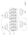
- FIG. 1is a circuit diagram of a conventional non-volatile memory array 100 .
- This array 100includes non-volatile memory cells 101 - 114 , select transistors 121 - 128 , metal bit lines 131 - 134 , diffusion bit lines 141 - 148 , and word lines 151 - 152 .
- metal bit lines 131 - 134are formed by metal interconnect lines formed over a semiconductor substrate
- diffusion bit lines 141 - 148are formed by conductively doped diffusion regions in the semiconductor substrate.
- the various elements of non-volatile memory array 100are described in more detail in U.S. Pat. No. 5,963,465 by Eitan, entitled “Symmetric Segmented Memory Array Architecture”.
- a critical parameter of non-volatile memory array 100is the area that it occupies in the semiconductor substrate. Non-volatile memory array 100 is therefore designed to occupy a minimum area in the substrate. Additional rows of non-volatile memory transistors can be added to expand array 100 along the vertical axis. In addition, the structure of memory cells 101 - 104 , 107 - 110 , diffusion bit lines 141 - 144 , select transistors 121 - 124 and metal bit lines 131 - 132 , which is shown in dashed lines, can be repeated to expand array 100 along the horizontal axis.
- non-volatile memory transistors of array 100are accessed through select transistors 121 - 128 .
- non-volatile memory transistor 102is read as follows. Select signals SEL[ 1 ] and SEL[ 2 ] are asserted high, thereby turning on select transistors 122 and 123 . As a result, metal bit line 131 is coupled to diffusion bit line 143 , and metal bit line 132 is coupled to diffusion bit line 142 . A source read voltage Vs is applied to diffusion bit line 143 through select transistor 122 and metal bit line 131 . A drain read voltage Vd is applied to diffusion bit line 142 through select transistor 123 and metal bit line 132 .
- Word line signal WL[ 0 ]is asserted high, thereby applying a logic high voltage to the gates of non-volatile memory transistors 101 - 107 .
- read currentflows from metal bit line 132 to metal bit line 131 through transistor 102 , with the magnitude of the read current depending on the threshold voltage of transistor 102 .
- the read currentis measured to provide information concerning the threshold voltage of transistor 102 (i.e., to determine whether transistor 102 is in a programmed or erased state).
- non-volatile transistor 102During a read of non-volatile transistor 102 , the current through transistor 102 is not protected from current that may flow to or from diffusion bit lines 141 and 144 through neighboring non-volatile transistors 101 and 103 , respectively. This is referred to as “neighbor effect”.
- the diffusion bit lines of array 100are typically pre-charged or pre-discharged prior to a read operation.
- the present inventionprovides a symmetric non-volatile memory array and method of operating that eliminates the neighbor effect, and does not require bit line pre-charge or pre-discharge.
- a methodfor reading a first non-volatile memory transistor in an array of non-volatile memory transistors, wherein the first non-volatile memory transistor has a drain coupled to the source of a second non-volatile memory transistor.
- the methodincludes the steps of (1) applying a read voltage to the gates of the first and second memory transistors, (2) applying a source voltage (Vs) to the source of the first memory transistor, (3) applying a drain voltage (Vd) to the drain of the first memory transistor and the source of the second memory transistor, and (4) applying a forcing voltage (Vf) to the drain of the second memory transistor.
- the drain voltage Vdis equal to the forcing voltage Vf.
- the source voltage Vscan be set to 0 Volts, such that another memory transistor, coupled to the source of the first transistor, will not disturb the read current through the first memory transistor. As a result, it is not necessary to pre-charge or pre-discharge bit lines of the array prior to a read operation.
- a non-volatile memory architectureis provided to allow the drain voltage Vd, the source voltage Vs and the forcing voltage Vf, to be applied to the non-volatile memory transistors in an array.
- this arrayincludes a first non-volatile memory transistor having a drain coupled to a first bit line, a second non-volatile memory transistor having a drain coupled to a second bit line and to the source of the first non-volatile memory transistor, and a third non-volatile memory transistor having a drain coupled to a third bit line and to the source of the second non-volatile memory transistor.
- meansare provided to allow the forcing voltage Vf to be applied to the first bit line, the drain voltage Vd to be applied to the second bit line, and a second read voltage to be applied to the third bit line in order to perform a read operation of the second non-volatile memory transistor.
- Each of the bit linescan include a diffusion bit line located in a semiconductor substrate, and a metal bit line located over the semiconductor substrate and coupled to the diffusion bit line.
- a select transistoris coupled between each metal bit line and a corresponding diffusion bit line.
- a non-volatile memory architecturein another embodiment, includes an array of non-volatile memory transistors arranged in rows and columns.
- a plurality of diffusion bit linesare provided, wherein each diffusion bit line is coupled to the drain of each transistor in one column of the array and the source of each transistor in an adjacent column of the array.
- a plurality of metal bit lines and a plurality of select transistorsare also provided. Each metal bit line is coupled to a dedicated pair of select transistors, wherein one of the select transistors is coupled to one of the diffusion bit lines, and the other select transistor is coupled to another one of the diffusion bit lines, wherein the diffusion bit lines are separated by two other diffusion bit lines. This spacing enables the forcing voltage Vf, the drain voltage Vd and the source voltage Vs to be applied in an efficient manner.
- Another embodiment of the present inventionprovides a method for reading a first non-volatile memory transistor in an array of non-volatile memory transistors, wherein the first non-volatile memory transistor has a drain coupled to the source of a second non-volatile memory transistor, and a source coupled to the drain of a third non-volatile memory transistor.
- the methodincludes the steps of (1) applying a read voltage to the gates of the first, second and third memory transistors, (2) applying a source voltage (Vs) to the source of the first memory transistor and the drain of the third memory transistor, (3) applying a drain voltage (Vd) to the drain of the first memory transistor and the source of the second memory transistor, (4) applying a first forcing voltage (Vf) to the drain of the second memory transistor; and (5) applying a second forcing voltage (Vfs) to the source of the third memory transistor.
- FIG. 1is a circuit diagram of a conventional high-density non-volatile memory array which experiences neighbor effect.
- FIG. 2is a circuit diagram of a symmetrical non-volatile memory array in accordance with one embodiment of the present invention.
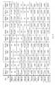
- FIG. 3is a table that defines bit line voltages and select voltages used to read non-volatile memory transistors of the array of FIG. 2 in accordance with one embodiment of the present invention.
- FIG. 4is a circuit diagram of a symmetrical non-volatile memory array in accordance with another embodiment of the present invention.
- FIG. 5is a table that defines bit line voltages and select voltages used to read non-volatile memory transistors of the array of FIG. 4 in accordance with one embodiment of the present invention.
- FIG. 2is a circuit diagram of a symmetrical non-volatile memory array 1000 in accordance with one embodiment of the present invention.
- Array 1000includes a pair of repeatable memory tiles 200 and 300 .
- Memory tile 200includes non-volatile memory transistors 201 - 212 , select transistors 220 - 225 , metal bit lines 230 - 232 , and diffusion bit lines 241 - 246 .
- memory tile 300includes non-volatile memory transistors 301 - 312 , select transistors 320 - 325 , metal bit lines 330 - 332 , and diffusion bit lines 341 - 347 .
- Memory tiles 200 and 300share word lines 250 - 251 and diffusion bit line 341 .
- array 1000can easily be expanded along the horizontal axis of FIG. 2 by attaching addition memory tiles identical to tiles 200 and 300 .
- array 1000can be expanded along the vertical axis of FIG. 2 by adding additional rows of non-volatile memory transistors, with corresponding word lines.
- the present inventionis not limited by the size of the array.
- Non-volatile memory transistors 201 - 206 and 301 - 306are located in a first row of array 1000 .
- the control gates of transistors 201 - 206 and 301 - 306are coupled to word line 250 .
- Non-volatile memory transistors 207 - 212 and 307 - 312are located in a second row of array 1000 .
- the control gates of transistors 207 - 212 and 307 - 312are coupled to word line 251 .
- Non-volatile memory array 1000is fabricated in a semiconductor substrate.
- Diffusion bit lines 241 - 246 and 341 - 347are formed by conductively doping regions of the semiconductor substrate.
- diffusion bit lines 241 - 246 and 341 - 347extend along the vertical axis of FIG. 2 .
- Each of diffusion bit lines 242 - 246 and 341 - 346is continuous with the source regions of memory transistors in one column of the array, and continuous with the drain regions of memory transistors in an adjacent column of the array.
- diffusion bit line 243is continuous with the sources of memory transistors 202 and 208 , and with the drains of memory transistors 203 and 209 .
- diffusion bit line 244is continuous with the sources of memory transistors 203 and 209 , and with the drains of memory transistors 204 and 210 .
- Select transistors 220 - 225 and 320 - 325which are fabricated in the semiconductor substrate, are used to couple diffusion bit lines 241 - 246 and 341 - 347 to metal bit lines 230 - 232 and 330 - 332 . More specifically, within memory tile 200 , select transistors 220 and 221 couple diffusion bit lines 241 and 244 , respectively, to metal bit line 230 . Similarly, select transistors 222 and 223 couple diffusion bit lines 243 and 246 , respectively, to metal bit line 232 . Finally, select transistors 224 and 225 couple diffusion bit lines 242 and 245 , respectively, to metal bit line 231 . Similar connections are provided between metal bit lines 330 - 332 and diffusion bit lines 341 - 346 in memory tile 300 .
- non-volatile memory transistors 201 - 212 and 301 - 312are n-channel devices. Thus, if electrons are stored in the floating gate of one of these memory transistors, then this memory transistor will exhibit a relatively high threshold voltage. This condition is referred to as the programmed state. Conversely, if electrons are removed from the floating gate of one of these memory transistors, then this memory transistor will exhibit a relatively low threshold voltage. This condition is referred to as the erased state.
- the steps of programming and erasing non-volatile memory transistorsare known to those skilled in the art, details concerning programming and erasing particular non-volatile memory transistors can be found in commonly owned, co-pending U.S. patent application Ser. No. 09/244,529, and U.S. Pat. Nos. 6,081,456 and 6,181,597, which are hereby incorporated by reference.
- a logic high read voltage(V WL ) is applied to word line 250 as the word line signal WL[ 0 ].
- this read voltage (V WL )can have a value equal to the V cc supply voltage.
- a logic low voltagesuch as ground, is applied to word line 251 as the word line signal WL[ 1 ], thereby turning off non-volatile memory transistors 207 - 212 and 307 - 312 in the second row.
- Logic high select signals SEL[ 2 ] and SEL[ 4 ]are asserted, thereby turning on select transistors 222 and 224 in memory tile 200 , and turning on select transistors 322 and 324 in memory tile 300 .
- a source read voltage Vsis applied to metal bit lines 232 and 332 as the MBL[ 2 ] and MBL[ 5 ] signals, respectively.
- the source read voltage Vsis thereby applied to the sources of transistors 202 and 302 through select transistors 222 and 322 , respectively.
- the source voltage Vshas a value of ground, or 0 Volts.
- a drain read voltage Vdis applied to metal bit lines 231 and 331 as the MBL[ 1 ] and MBL[ 4 ] signals, respectively.
- the drain read voltage Vdis thereby applied to the drains of transistors 202 and 302 through select transistors 224 and 324 , respectively.
- the drain voltage Vdis a positive voltage of about 2 Volts.
- a logic high select signal SEL[ 0 ]is asserted, thereby turning on select transistors 220 and 320 .
- a forcing voltage Vfis applied to metal bit lines 230 and 330 , as the MBL[ 0 ] AND MBL[ 3 ] signals, respectively.
- the forcing voltage Vfis thereby applied to the drains of transistors 201 and 301 through select transistors 220 and 320 , respectively.
- the forcing voltage Vfis set equal to the drain voltage Vd.
- the forcing voltage Vfis set to a positive voltage of about 2 Volts.
- transistor 202has a low threshold voltage (i.e., is in the erased condition)
- a substantial read currentwill flow through this transistor. That is, read current will flow from diffusion bit line 242 , which is held at 2 Volts, to diffusion bit line 243 , which is held at 0 Volts.
- diffusion bit line 241Because neighboring diffusion bit line 241 is held at the same voltage as diffusion bit line 242 , diffusion bit line 241 does not tend to increase or reduce the read current through transistor 202 . That is, even if neighboring transistor 201 has a low threshold voltage, no current will flow through this transistor 201 because the source and drain of this transistor are held at the same voltage. In this manner, transistor 202 is protected from the neighbor effect on the drain side.
- diffusion bit line 242is held at the ground supply voltage, any charge on diffusion bit line 244 will not increase or reduce the read current through memory transistor 202 . That is, even if neighboring memory transistor 203 has a low threshold voltage, any charge on diffusion bit line 244 will simply be discharged to the ground supply voltage. In this manner, transistor 202 is protected from the neighbor effect on the source side.
- non-volatile memory transistor 202has a high threshold voltage (i.e., this transistor is programmed), then no significant read current will flow through this transistor 202 .
- transistors 202 and 302Other non-volatile memory transistors in array 1000 are accessed in the same manner as transistors 202 and 302 . Although both transistors 202 and 302 were read in the example described above, either one of transistors 202 and 302 can be read independently. For example, transistor 202 can be read in the manner described above, while metal bit lines 330 - 332 are left floating, such that transistor 302 is not read.
- FIG. 3is a table 350 that defines the voltages MBL[ 5 : 0 ] and SEL[ 5 : 0 ] used to read memory transistors 201 - 206 and 301 - 305 .
- Table 350assumes a logic high word line signal WL[ 0 ] and a logic low word line signal WL[ 1 ].
- Non-volatile memory transistors 207 - 212 and 307 - 311are read in a manner similar to non-volatile memory transistors 201 - 206 and 301 - 305 (but with word line signal WL[ 1 ] asserted high and word line signal WL[ 0 ] de-asserted low).
- non-volatile memory transistors 306 and 312cannot be read in the present embodiment, as there is no memory tile coupled to the right side of memory tile 300 . However, if a memory tile were coupled to the right side of memory tile 300 , then memory transistors 306 and 312 would be read in the same manner as memory transistors 206 and 212 .
- the voltages listed in table 350take into consideration the possible expansion of array 1000 to include memory tiles to the left and right.
- FIG. 4is a circuit diagram of a symmetrical non-volatile memory array 2000 in accordance with another embodiment of the present invention.
- Array 2000includes a pair of repeatable memory tiles 400 and 500 .
- Memory tile 400includes non-volatile memory transistors 401 - 416 , select transistors 420 - 427 , metal bit lines 430 - 433 , and diffusion bit lines 441 - 448 .
- memory tile 500includes non-volatile memory transistors 501 - 516 , select transistors 520 - 527 , metal bit lines 530 - 533 , and diffusion bit lines 541 - 548 .
- Memory tiles 400 and 500share word lines 450 - 451 and diffusion bit line 541 .
- Nonvolatile memory transistors 401 - 408 and 501 - 508are located in a first row of array 2000 .
- the control gates of transistors 401 - 408 and 501 - 508are coupled to word line 450 .
- Nonvolatile memory transistors 409 - 416 and 509 - 516are located in a second row of array 2000 .
- the control gates of transistors 409 - 416 and 509 - 516are coupled to word line 451 .
- Nonvolatile memory transistors 401 - 416 and 501 - 516are substantially identical to non-volatile memory transistors 201 - 212 and 301 - 312 (FIG. 2) in the described embodiment.
- Non-volatile memory array 2000is fabricated in a semiconductor substrate.
- Diffusion bit lines 441 - 448 and 541 - 548are formed by conductively doping regions of the semiconductor substrate.
- Diffusion bit lines 441 - 448 and 541 - 548are similar to diffusion bit lines 241 - 246 and 341 - 346 of FIG. 2 .
- Select transistors 420 - 427 and 520 - 527which are fabricated in the semiconductor substrate, are used to couple diffusion bit lines 441 - 448 and 541 - 548 to metal bit lines 430 - 433 and 530 - 533 . More specifically, within memory tile 400 , select transistors 420 and 421 couple diffusion bit lines 441 and 445 , respectively, to metal bit line 430 . Similarly, select transistors 422 and 423 couple diffusion bit lines 443 and 447 , respectively, to metal bit line 432 . Select transistors 424 and 425 couple diffusion bit lines 442 and 446 , respectively, to metal bit line 431 .
- select transistors 426 and 427couple diffusion bit lines 444 and 448 , respectively, to metal bit line 433 . Similar connections are provided between metal bit lines 530 - 533 and diffusion bit lines 541 - 548 in memory tile 500 . In this manner, each metal bit line is capable of being coupled to a first diffusion bit line, and a second diffusion bit line that is separated from the first diffusion bit line by three other diffusion bit lines.
- a non-volatile memory transistor in array 2000is read in the same manner as a non-volatile memory transistor in array 1000 .
- non-volatile memory transistor 406is read as follows.
- a logic high read voltage (V WL )is applied to word line 450
- a logic low voltage, such as ground,is applied to word line 451 .
- the select signals SEL[ 1 ], SEL[ 3 ] and SEL[ 5 ]are all asserted high, thereby turning on select transistors 421 , 423 and 425 .
- a source read voltage Vsis applied to metal bit line 432 as the MBL[ 2 ] signal. The source read voltage Vs is thereby applied to the source of transistor 406 through select transistor 423 .
- a drain read voltage Vdis applied to metal bit line 431 as the MBL[ 1 ] signal.
- the drain read voltage Vdis thereby applied to the drain of transistor 406 through select transistor 425 .
- a forcing voltage Vfis applied to metal bit lines 430 as the MBL[ 0 ] signal.
- the forcing voltage Vfis thereby applied to the drain of transistor 405 through select transistor 421 .
- Metal bit lines 433 and 530 - 533are left floating in the present example. Under these conditions, non-volatile memory transistor 406 is read in the manner described above.
- array 2000is operated using two forcing voltages.
- a second forcing voltage Vfsis applied to the source of a second adjacent transistor.
- the same procedure described aboveis performed.
- the select signal SEL[ 7 ]is also asserted, thereby turning on select transistor 427 .
- the second forcing voltage Vfsis applied to metal bit line 433 as the MBL[ 3 ] signal.
- the second forcing voltage Vfsis thereby applied to the source of non-volatile memory transistor 407 (through turned on select transistor 427 and diffusion bit line 448 ).
- the second forcing voltage Vfsis set equal to the source voltage Vs.
- the second forcing voltage Vfsis set to the ground voltage of about 0 Volts. Because neighboring diffusion bit line 448 is held at the same voltage as diffusion bit line 447 , diffusion bit line 448 does not tend to increase or reduce the read current through transistor 406 . That is, even if neighboring transistor 407 has a low threshold voltage, no current will flow through this transistor 407 because the source and drain of this transistor are held at the same voltage. In this manner, transistor 406 is protected from the neighbor effect on the source side.
- FIG. 4is a table 450 that defines the voltages MBL[ 7 : 0 ] and SEL[ 7 : 0 ] used to read memory transistors 401 - 408 .
- Table 450assumes a logic high word line signal WL[ 0 ] and a logic low word line signal WL[ 1 ].
- Non-volatile memory transistors 409 - 416 and 501 - 516are read in a manner similar to non-volatile memory transistors 401 - 408 . Note that non-volatile memory transistors 508 and 516 cannot be read in the present embodiment, as there is no memory tile coupled to the right side of memory tile 500 .
- memory transistors 508 and 516would be read in the same manner as memory transistor 408 .
- the voltages listed in table 450take into consideration the possible expansion of array 2000 to include memory tiles to the left and right.
Landscapes
- Non-Volatile Memory (AREA)
- Read Only Memory (AREA)
Abstract
Description
Claims (19)
Priority Applications (1)
| Application Number | Priority Date | Filing Date | Title |
|---|---|---|---|
| US09/821,336US6351415B1 (en) | 2001-03-28 | 2001-03-28 | Symmetrical non-volatile memory array architecture without neighbor effect |
Applications Claiming Priority (1)
| Application Number | Priority Date | Filing Date | Title |
|---|---|---|---|
| US09/821,336US6351415B1 (en) | 2001-03-28 | 2001-03-28 | Symmetrical non-volatile memory array architecture without neighbor effect |
Publications (1)
| Publication Number | Publication Date |
|---|---|
| US6351415B1true US6351415B1 (en) | 2002-02-26 |
Family
ID=25233111
Family Applications (1)
| Application Number | Title | Priority Date | Filing Date |
|---|---|---|---|
| US09/821,336Expired - LifetimeUS6351415B1 (en) | 2001-03-28 | 2001-03-28 | Symmetrical non-volatile memory array architecture without neighbor effect |
Country Status (1)
| Country | Link |
|---|---|
| US (1) | US6351415B1 (en) |
Cited By (52)
| Publication number | Priority date | Publication date | Assignee | Title |
|---|---|---|---|---|
| US20020196698A1 (en)* | 1997-12-12 | 2002-12-26 | Boaz Eitan | Symmetric segmented memory array architecture |
| US20030039153A1 (en)* | 2001-01-18 | 2003-02-27 | Eduardo Maayan | EEPROM array and method for operation thereof |
| US20040153620A1 (en)* | 2003-01-30 | 2004-08-05 | Shai Eisen | Address scramble |
| US20040218426A1 (en)* | 2003-04-29 | 2004-11-04 | Oleg Dadashev | Apparatus and methods for multi-level sensing in a memory array |
| US20050088878A1 (en)* | 2003-10-27 | 2005-04-28 | Tower Semiconductor Ltd. | Neighbor effect cancellation in memory array architecture |
| US6917544B2 (en) | 2002-07-10 | 2005-07-12 | Saifun Semiconductors Ltd. | Multiple use memory chip |
| US20050180212A1 (en)* | 2004-02-16 | 2005-08-18 | Matsushita Electric Industrial Co., Ltd. | Non-volatile semiconductor memory device |
| US20050232024A1 (en)* | 2004-04-19 | 2005-10-20 | Shahar Atir | Method for reading a memory array with neighbor effect cancellation |
| US6963505B2 (en) | 2002-10-29 | 2005-11-08 | Aifun Semiconductors Ltd. | Method circuit and system for determining a reference voltage |
| US6992932B2 (en) | 2002-10-29 | 2006-01-31 | Saifun Semiconductors Ltd | Method circuit and system for read error detection in a non-volatile memory array |
| US20060034122A1 (en)* | 2004-08-12 | 2006-02-16 | Yoram Betser | Dynamic matching of signal path and reference path for sensing |
| US20060036803A1 (en)* | 2004-08-16 | 2006-02-16 | Mori Edan | Non-volatile memory device controlled by a micro-controller |
| US20060056240A1 (en)* | 2004-04-01 | 2006-03-16 | Saifun Semiconductors, Ltd. | Method, circuit and system for erasing one or more non-volatile memory cells |
| US20060068551A1 (en)* | 2004-09-27 | 2006-03-30 | Saifun Semiconductors, Ltd. | Method for embedding NROM |
| US20060126382A1 (en)* | 2004-12-09 | 2006-06-15 | Eduardo Maayan | Method for reading non-volatile memory cells |
| US20060126396A1 (en)* | 2002-01-31 | 2006-06-15 | Saifun Semiconductors, Ltd. | Method, system, and circuit for operating a non-volatile memory array |
| US7064983B2 (en) | 2001-04-05 | 2006-06-20 | Saifum Semiconductors Ltd. | Method for programming a reference cell |
| US20060146624A1 (en)* | 2004-12-02 | 2006-07-06 | Saifun Semiconductors, Ltd. | Current folding sense amplifier |
| US20060158940A1 (en)* | 2005-01-19 | 2006-07-20 | Saifun Semiconductors, Ltd. | Partial erase verify |
| US20060211188A1 (en)* | 2004-10-14 | 2006-09-21 | Saifun Semiconductors Ltd. | Non-volatile memory structure and method of fabrication |
| US20060262598A1 (en)* | 1997-08-01 | 2006-11-23 | Saifun Semiconductors Ltd. | Two bit non-volatile electrically erasable and programmable semiconductor memory cell utilizing asymmetrical charge trapping |
| US20060285386A1 (en)* | 2005-06-15 | 2006-12-21 | Saifun Semiconductors, Ltd. | Accessing an NROM array |
| US20060285408A1 (en)* | 2005-06-17 | 2006-12-21 | Saifun Semiconductors, Ltd. | Method circuit and system for compensating for temperature induced margin loss in non-volatile memory cells |
| US20070032016A1 (en)* | 2001-11-19 | 2007-02-08 | Saifun Semiconductors Ltd. | Protective layer in memory device and method therefor |
| US20070036007A1 (en)* | 2005-08-09 | 2007-02-15 | Saifun Semiconductors, Ltd. | Sticky bit buffer |
| US20070051982A1 (en)* | 2005-07-18 | 2007-03-08 | Saifun Semiconductors Ltd. | Dense non-volatile memory array and method of fabrication |
| US20070096199A1 (en)* | 2005-09-08 | 2007-05-03 | Eli Lusky | Method of manufacturing symmetric arrays |
| US7221138B2 (en) | 2005-09-27 | 2007-05-22 | Saifun Semiconductors Ltd | Method and apparatus for measuring charge pump output current |
| US20070120180A1 (en)* | 2005-11-25 | 2007-05-31 | Boaz Eitan | Transition areas for dense memory arrays |
| US20070133276A1 (en)* | 2003-09-16 | 2007-06-14 | Eli Lusky | Operating array cells with matched reference cells |
| US20070141788A1 (en)* | 2005-05-25 | 2007-06-21 | Ilan Bloom | Method for embedding non-volatile memory with logic circuitry |
| US20070153575A1 (en)* | 2006-01-03 | 2007-07-05 | Saifun Semiconductors, Ltd. | Method, system, and circuit for operating a non-volatile memory array |
| US20070159880A1 (en)* | 2006-01-12 | 2007-07-12 | Boaz Eitan | Secondary injection for NROM |
| US20070168637A1 (en)* | 2003-01-31 | 2007-07-19 | Yan Polansky | Memory array programming circuit and a method for using the circuit |
| US20070173017A1 (en)* | 2006-01-20 | 2007-07-26 | Saifun Semiconductors, Ltd. | Advanced non-volatile memory array and method of fabrication thereof |
| US20070194835A1 (en)* | 2006-02-21 | 2007-08-23 | Alexander Kushnarenko | Circuit and method for powering up an integrated circuit and an integrated circuit utilizing same |
| US20070195607A1 (en)* | 2006-02-21 | 2007-08-23 | Saifun Semiconductors Ltd. | Nrom non-volatile memory and mode of operation |
| US20070196982A1 (en)* | 2006-02-21 | 2007-08-23 | Saifun Semiconductors Ltd. | Nrom non-volatile mode of operation |
| US20070253248A1 (en)* | 2006-04-27 | 2007-11-01 | Eduardo Maayan | Method for programming a reference cell |
| US20070255889A1 (en)* | 2006-03-22 | 2007-11-01 | Yoav Yogev | Non-volatile memory device and method of operating the device |
| US7317633B2 (en) | 2004-07-06 | 2008-01-08 | Saifun Semiconductors Ltd | Protection of NROM devices from charge damage |
| US20080094127A1 (en)* | 2006-09-18 | 2008-04-24 | Yoram Betser | Measuring and controlling current consumption and output current of charge pumps |
| US20080239599A1 (en)* | 2007-04-01 | 2008-10-02 | Yehuda Yizraeli | Clamping Voltage Events Such As ESD |
| US7522453B1 (en)* | 2007-12-20 | 2009-04-21 | Actel Corporation | Non-volatile memory with source-side column select |
| US20090121281A1 (en)* | 2007-11-14 | 2009-05-14 | Keita Takahashi | Semiconductor memory device |
| US7535765B2 (en) | 2004-12-09 | 2009-05-19 | Saifun Semiconductors Ltd. | Non-volatile memory device and method for reading cells |
| US7590001B2 (en) | 2007-12-18 | 2009-09-15 | Saifun Semiconductors Ltd. | Flash memory with optimized write sector spares |
| US7638835B2 (en) | 2006-02-28 | 2009-12-29 | Saifun Semiconductors Ltd. | Double density NROM with nitride strips (DDNS) |
| US7668017B2 (en) | 2005-08-17 | 2010-02-23 | Saifun Semiconductors Ltd. | Method of erasing non-volatile memory cells |
| US7675782B2 (en) | 2002-10-29 | 2010-03-09 | Saifun Semiconductors Ltd. | Method, system and circuit for programming a non-volatile memory array |
| US8053812B2 (en) | 2005-03-17 | 2011-11-08 | Spansion Israel Ltd | Contact in planar NROM technology |
| TWI416526B (en)* | 2011-09-21 | 2013-11-21 | Floadia Corp | Nonvolatile semiconductor memory device |
Citations (2)
| Publication number | Priority date | Publication date | Assignee | Title |
|---|---|---|---|---|
| US5963465A (en) | 1997-12-12 | 1999-10-05 | Saifun Semiconductors, Ltd. | Symmetric segmented memory array architecture |
| US6157570A (en)* | 1999-02-04 | 2000-12-05 | Tower Semiconductor Ltd. | Program/erase endurance of EEPROM memory cells |
- 2001
- 2001-03-28USUS09/821,336patent/US6351415B1/ennot_activeExpired - Lifetime
Patent Citations (2)
| Publication number | Priority date | Publication date | Assignee | Title |
|---|---|---|---|---|
| US5963465A (en) | 1997-12-12 | 1999-10-05 | Saifun Semiconductors, Ltd. | Symmetric segmented memory array architecture |
| US6157570A (en)* | 1999-02-04 | 2000-12-05 | Tower Semiconductor Ltd. | Program/erase endurance of EEPROM memory cells |
Cited By (90)
| Publication number | Priority date | Publication date | Assignee | Title |
|---|---|---|---|---|
| US20090032862A1 (en)* | 1997-08-01 | 2009-02-05 | Eduardo Maayan | Non-volatile memory cell and non-volatile memory device using said cell |
| US20060262598A1 (en)* | 1997-08-01 | 2006-11-23 | Saifun Semiconductors Ltd. | Two bit non-volatile electrically erasable and programmable semiconductor memory cell utilizing asymmetrical charge trapping |
| US7405969B2 (en) | 1997-08-01 | 2008-07-29 | Saifun Semiconductors Ltd. | Non-volatile memory cell and non-volatile memory devices |
| US20080111177A1 (en)* | 1997-08-01 | 2008-05-15 | Eduardo Maayan | Non-volatile memory cell and non-volatile memory device using said cell |
| US6633496B2 (en)* | 1997-12-12 | 2003-10-14 | Saifun Semiconductors Ltd. | Symmetric architecture for memory cells having widely spread metal bit lines |
| US6704217B2 (en)* | 1997-12-12 | 2004-03-09 | Saifun Semiconductors Ltd. | Symmetric segmented memory array architecture |
| US20020196698A1 (en)* | 1997-12-12 | 2002-12-26 | Boaz Eitan | Symmetric segmented memory array architecture |
| US20030039153A1 (en)* | 2001-01-18 | 2003-02-27 | Eduardo Maayan | EEPROM array and method for operation thereof |
| US7518908B2 (en) | 2001-01-18 | 2009-04-14 | Saifun Semiconductors Ltd. | EEPROM array and method for operation thereof |
| US7064983B2 (en) | 2001-04-05 | 2006-06-20 | Saifum Semiconductors Ltd. | Method for programming a reference cell |
| US20070032016A1 (en)* | 2001-11-19 | 2007-02-08 | Saifun Semiconductors Ltd. | Protective layer in memory device and method therefor |
| US20060126396A1 (en)* | 2002-01-31 | 2006-06-15 | Saifun Semiconductors, Ltd. | Method, system, and circuit for operating a non-volatile memory array |
| US7420848B2 (en) | 2002-01-31 | 2008-09-02 | Saifun Semiconductors Ltd. | Method, system, and circuit for operating a non-volatile memory array |
| US20060152975A1 (en)* | 2002-07-10 | 2006-07-13 | Eduardo Maayan | Multiple use memory chip |
| US6917544B2 (en) | 2002-07-10 | 2005-07-12 | Saifun Semiconductors Ltd. | Multiple use memory chip |
| US7738304B2 (en) | 2002-07-10 | 2010-06-15 | Saifun Semiconductors Ltd. | Multiple use memory chip |
| US7675782B2 (en) | 2002-10-29 | 2010-03-09 | Saifun Semiconductors Ltd. | Method, system and circuit for programming a non-volatile memory array |
| US6963505B2 (en) | 2002-10-29 | 2005-11-08 | Aifun Semiconductors Ltd. | Method circuit and system for determining a reference voltage |
| US6992932B2 (en) | 2002-10-29 | 2006-01-31 | Saifun Semiconductors Ltd | Method circuit and system for read error detection in a non-volatile memory array |
| US6967896B2 (en) | 2003-01-30 | 2005-11-22 | Saifun Semiconductors Ltd | Address scramble |
| US20040153620A1 (en)* | 2003-01-30 | 2004-08-05 | Shai Eisen | Address scramble |
| US20070168637A1 (en)* | 2003-01-31 | 2007-07-19 | Yan Polansky | Memory array programming circuit and a method for using the circuit |
| US7743230B2 (en) | 2003-01-31 | 2010-06-22 | Saifun Semiconductors Ltd. | Memory array programming circuit and a method for using the circuit |
| US20040218426A1 (en)* | 2003-04-29 | 2004-11-04 | Oleg Dadashev | Apparatus and methods for multi-level sensing in a memory array |
| US7142464B2 (en) | 2003-04-29 | 2006-11-28 | Saifun Semiconductors Ltd. | Apparatus and methods for multi-level sensing in a memory array |
| US20070133276A1 (en)* | 2003-09-16 | 2007-06-14 | Eli Lusky | Operating array cells with matched reference cells |
| US7457183B2 (en) | 2003-09-16 | 2008-11-25 | Saifun Semiconductors Ltd. | Operating array cells with matched reference cells |
| US20050088878A1 (en)* | 2003-10-27 | 2005-04-28 | Tower Semiconductor Ltd. | Neighbor effect cancellation in memory array architecture |
| US6937523B2 (en) | 2003-10-27 | 2005-08-30 | Tower Semiconductor Ltd. | Neighbor effect cancellation in memory array architecture |
| US7123510B2 (en) | 2004-02-16 | 2006-10-17 | Matsushita Electric Industrial Co., Ltd. | Non-volatile semiconductor memory device |
| US20050180212A1 (en)* | 2004-02-16 | 2005-08-18 | Matsushita Electric Industrial Co., Ltd. | Non-volatile semiconductor memory device |
| US7532529B2 (en) | 2004-03-29 | 2009-05-12 | Saifun Semiconductors Ltd. | Apparatus and methods for multi-level sensing in a memory array |
| US7652930B2 (en) | 2004-04-01 | 2010-01-26 | Saifun Semiconductors Ltd. | Method, circuit and system for erasing one or more non-volatile memory cells |
| US20060056240A1 (en)* | 2004-04-01 | 2006-03-16 | Saifun Semiconductors, Ltd. | Method, circuit and system for erasing one or more non-volatile memory cells |
| US7755938B2 (en) | 2004-04-19 | 2010-07-13 | Saifun Semiconductors Ltd. | Method for reading a memory array with neighbor effect cancellation |
| US20050232024A1 (en)* | 2004-04-19 | 2005-10-20 | Shahar Atir | Method for reading a memory array with neighbor effect cancellation |
| US7317633B2 (en) | 2004-07-06 | 2008-01-08 | Saifun Semiconductors Ltd | Protection of NROM devices from charge damage |
| US7466594B2 (en) | 2004-08-12 | 2008-12-16 | Saifun Semiconductors Ltd. | Dynamic matching of signal path and reference path for sensing |
| US7095655B2 (en)* | 2004-08-12 | 2006-08-22 | Saifun Semiconductors Ltd. | Dynamic matching of signal path and reference path for sensing |
| US20070171717A1 (en)* | 2004-08-12 | 2007-07-26 | Saifun Semiconductors Ltd. | Dynamic matching of signal path and reference path for sensing |
| US20060034122A1 (en)* | 2004-08-12 | 2006-02-16 | Yoram Betser | Dynamic matching of signal path and reference path for sensing |
| US20060036803A1 (en)* | 2004-08-16 | 2006-02-16 | Mori Edan | Non-volatile memory device controlled by a micro-controller |
| US20060068551A1 (en)* | 2004-09-27 | 2006-03-30 | Saifun Semiconductors, Ltd. | Method for embedding NROM |
| US20100173464A1 (en)* | 2004-10-14 | 2010-07-08 | Eli Lusky | Non-volatile memory structure and method of fabrication |
| US7964459B2 (en) | 2004-10-14 | 2011-06-21 | Spansion Israel Ltd. | Non-volatile memory structure and method of fabrication |
| US7638850B2 (en) | 2004-10-14 | 2009-12-29 | Saifun Semiconductors Ltd. | Non-volatile memory structure and method of fabrication |
| US20060211188A1 (en)* | 2004-10-14 | 2006-09-21 | Saifun Semiconductors Ltd. | Non-volatile memory structure and method of fabrication |
| US20060146624A1 (en)* | 2004-12-02 | 2006-07-06 | Saifun Semiconductors, Ltd. | Current folding sense amplifier |
| US7257025B2 (en) | 2004-12-09 | 2007-08-14 | Saifun Semiconductors Ltd | Method for reading non-volatile memory cells |
| US7535765B2 (en) | 2004-12-09 | 2009-05-19 | Saifun Semiconductors Ltd. | Non-volatile memory device and method for reading cells |
| US20060126382A1 (en)* | 2004-12-09 | 2006-06-15 | Eduardo Maayan | Method for reading non-volatile memory cells |
| US7468926B2 (en) | 2005-01-19 | 2008-12-23 | Saifun Semiconductors Ltd. | Partial erase verify |
| US7369440B2 (en) | 2005-01-19 | 2008-05-06 | Saifun Semiconductors Ltd. | Method, circuit and systems for erasing one or more non-volatile memory cells |
| US20060158940A1 (en)* | 2005-01-19 | 2006-07-20 | Saifun Semiconductors, Ltd. | Partial erase verify |
| US8053812B2 (en) | 2005-03-17 | 2011-11-08 | Spansion Israel Ltd | Contact in planar NROM technology |
| US20070141788A1 (en)* | 2005-05-25 | 2007-06-21 | Ilan Bloom | Method for embedding non-volatile memory with logic circuitry |
| US8400841B2 (en) | 2005-06-15 | 2013-03-19 | Spansion Israel Ltd. | Device to program adjacent storage cells of different NROM cells |
| US20060285386A1 (en)* | 2005-06-15 | 2006-12-21 | Saifun Semiconductors, Ltd. | Accessing an NROM array |
| US7184313B2 (en) | 2005-06-17 | 2007-02-27 | Saifun Semiconductors Ltd. | Method circuit and system for compensating for temperature induced margin loss in non-volatile memory cells |
| US20060285408A1 (en)* | 2005-06-17 | 2006-12-21 | Saifun Semiconductors, Ltd. | Method circuit and system for compensating for temperature induced margin loss in non-volatile memory cells |
| US7786512B2 (en) | 2005-07-18 | 2010-08-31 | Saifun Semiconductors Ltd. | Dense non-volatile memory array and method of fabrication |
| US20070051982A1 (en)* | 2005-07-18 | 2007-03-08 | Saifun Semiconductors Ltd. | Dense non-volatile memory array and method of fabrication |
| US20070036007A1 (en)* | 2005-08-09 | 2007-02-15 | Saifun Semiconductors, Ltd. | Sticky bit buffer |
| US7668017B2 (en) | 2005-08-17 | 2010-02-23 | Saifun Semiconductors Ltd. | Method of erasing non-volatile memory cells |
| US20070096199A1 (en)* | 2005-09-08 | 2007-05-03 | Eli Lusky | Method of manufacturing symmetric arrays |
| US7221138B2 (en) | 2005-09-27 | 2007-05-22 | Saifun Semiconductors Ltd | Method and apparatus for measuring charge pump output current |
| US20070120180A1 (en)* | 2005-11-25 | 2007-05-31 | Boaz Eitan | Transition areas for dense memory arrays |
| US20070153575A1 (en)* | 2006-01-03 | 2007-07-05 | Saifun Semiconductors, Ltd. | Method, system, and circuit for operating a non-volatile memory array |
| US7352627B2 (en) | 2006-01-03 | 2008-04-01 | Saifon Semiconductors Ltd. | Method, system, and circuit for operating a non-volatile memory array |
| US20070159880A1 (en)* | 2006-01-12 | 2007-07-12 | Boaz Eitan | Secondary injection for NROM |
| US7808818B2 (en) | 2006-01-12 | 2010-10-05 | Saifun Semiconductors Ltd. | Secondary injection for NROM |
| US20070173017A1 (en)* | 2006-01-20 | 2007-07-26 | Saifun Semiconductors, Ltd. | Advanced non-volatile memory array and method of fabrication thereof |
| US20070194835A1 (en)* | 2006-02-21 | 2007-08-23 | Alexander Kushnarenko | Circuit and method for powering up an integrated circuit and an integrated circuit utilizing same |
| US7760554B2 (en) | 2006-02-21 | 2010-07-20 | Saifun Semiconductors Ltd. | NROM non-volatile memory and mode of operation |
| US7692961B2 (en) | 2006-02-21 | 2010-04-06 | Saifun Semiconductors Ltd. | Method, circuit and device for disturb-control of programming nonvolatile memory cells by hot-hole injection (HHI) and by channel hot-electron (CHE) injection |
| US8253452B2 (en) | 2006-02-21 | 2012-08-28 | Spansion Israel Ltd | Circuit and method for powering up an integrated circuit and an integrated circuit utilizing same |
| US20070196982A1 (en)* | 2006-02-21 | 2007-08-23 | Saifun Semiconductors Ltd. | Nrom non-volatile mode of operation |
| US20070195607A1 (en)* | 2006-02-21 | 2007-08-23 | Saifun Semiconductors Ltd. | Nrom non-volatile memory and mode of operation |
| US7638835B2 (en) | 2006-02-28 | 2009-12-29 | Saifun Semiconductors Ltd. | Double density NROM with nitride strips (DDNS) |
| US20070255889A1 (en)* | 2006-03-22 | 2007-11-01 | Yoav Yogev | Non-volatile memory device and method of operating the device |
| US20070253248A1 (en)* | 2006-04-27 | 2007-11-01 | Eduardo Maayan | Method for programming a reference cell |
| US7701779B2 (en) | 2006-04-27 | 2010-04-20 | Sajfun Semiconductors Ltd. | Method for programming a reference cell |
| US7605579B2 (en) | 2006-09-18 | 2009-10-20 | Saifun Semiconductors Ltd. | Measuring and controlling current consumption and output current of charge pumps |
| US20080094127A1 (en)* | 2006-09-18 | 2008-04-24 | Yoram Betser | Measuring and controlling current consumption and output current of charge pumps |
| US20080239599A1 (en)* | 2007-04-01 | 2008-10-02 | Yehuda Yizraeli | Clamping Voltage Events Such As ESD |
| US8013378B2 (en) | 2007-11-14 | 2011-09-06 | Panasonic Corporation | Memory device having additional selection transistors and main bit lines |
| US20090121281A1 (en)* | 2007-11-14 | 2009-05-14 | Keita Takahashi | Semiconductor memory device |
| US7590001B2 (en) | 2007-12-18 | 2009-09-15 | Saifun Semiconductors Ltd. | Flash memory with optimized write sector spares |
| US7522453B1 (en)* | 2007-12-20 | 2009-04-21 | Actel Corporation | Non-volatile memory with source-side column select |
| TWI416526B (en)* | 2011-09-21 | 2013-11-21 | Floadia Corp | Nonvolatile semiconductor memory device |
Similar Documents
| Publication | Publication Date | Title |
|---|---|---|
| US6351415B1 (en) | Symmetrical non-volatile memory array architecture without neighbor effect | |
| US5065364A (en) | Apparatus for providing block erasing in a flash EPROM | |
| US6885585B2 (en) | NROM NOR array | |
| US6716700B2 (en) | Method of forming memory arrays based on a triple-polysilicon source-side injection non-volatile memory cell | |
| US5896340A (en) | Multiple array architecture for analog or multi-bit-cell memory | |
| US5740107A (en) | Nonvolatile integrated circuit memories having separate read/write paths | |
| US6407941B1 (en) | Segmented non-volatile memory array with multiple sources having improved source line decode circuitry | |
| US6222774B1 (en) | Data-erasable non-volatile semiconductor memory device | |
| US8081509B2 (en) | Non-volatile memory device and method of operation therefor | |
| KR100374522B1 (en) | Nonvolatile semiconductor memory device capable of reducing memory array area | |
| JPH06215587A (en) | Nonvolatile memory device | |
| US7663922B2 (en) | Non-volatile semiconductor memory devices with lower and upper bit lines sharing a voltage control block, and memory cards and systems having the same | |
| JPH11330426A (en) | Nonvolatile semiconductor memory device and method of manufacturing the same | |
| US7623383B2 (en) | Three-level non-volatile semiconductor memory devices with lower and upper bit lines sharing a voltage control block | |
| US4845538A (en) | E2 prom cell including isolated control diffusion | |
| EP1214715B1 (en) | 1 transistor cell for eeprom application | |
| US20080130367A1 (en) | Byte-Erasable Nonvolatile Memory Devices | |
| US20030218910A1 (en) | Semiconductor memory device capable of accurately writing data | |
| US6510084B2 (en) | Column decoder with increased immunity to high voltage breakdown | |
| US7672160B2 (en) | 3-level non-volatile semiconductor memory devices and related methods | |
| US6493268B1 (en) | Circuit device for performing hierarchic row decoding in non-volatile memory devices | |
| US5943268A (en) | Non-volatile latch having PMOS floating gate memory cells | |
| KR100629987B1 (en) | Flash memory architecture using three-layer metal wiring | |
| US7301820B2 (en) | Non-volatile memory dynamic operations | |
| US6819593B2 (en) | Architecture to suppress bit-line leakage |
Legal Events
| Date | Code | Title | Description |
|---|---|---|---|
| AS | Assignment | Owner name:TOWER SEMICONDUCTOR LTD., ISRAEL Free format text:ASSIGNMENT OF ASSIGNORS INTEREST;ASSIGNOR:KUSHNARENKO, ALEXANDER;REEL/FRAME:011664/0128 Effective date:20010304 | |
| STCF | Information on status: patent grant | Free format text:PATENTED CASE | |
| FPAY | Fee payment | Year of fee payment:4 | |
| FPAY | Fee payment | Year of fee payment:8 | |
| FEPP | Fee payment procedure | Free format text:PAYOR NUMBER ASSIGNED (ORIGINAL EVENT CODE: ASPN); ENTITY STATUS OF PATENT OWNER: LARGE ENTITY | |
| AS | Assignment | Owner name:APPLE INC., CALIFORNIA Free format text:SECURITY AGREEMENT;ASSIGNOR:ELPIDA MEMORY, INC.;REEL/FRAME:028209/0477 Effective date:20120410 | |
| FPAY | Fee payment | Year of fee payment:12 | |
| AS | Assignment | Owner name:ELPIDA MEMORY INC., JAPAN Free format text:SECURITY AGREEMENT;ASSIGNOR:PS4 LUXCO S.A.R.L.;REEL/FRAME:032414/0261 Effective date:20130726 | |
| AS | Assignment | Owner name:ELPIDA MEMORY, INC., JAPAN Free format text:RELEASE BY SECURED PARTY;ASSIGNOR:APPLE, INC;REEL/FRAME:032331/0637 Effective date:20140114 | |
| AS | Assignment | Owner name:PS4 LUXCO S.A.R.L., LUXEMBOURG Free format text:ASSIGNMENT OF ASSIGNORS INTEREST;ASSIGNOR:ELPIDA MEMORY, INC.;REEL/FRAME:032899/0588 Effective date:20130726 | |
| AS | Assignment | Owner name:PS5 LUXCO S.A.R.L., LUXEMBOURG Free format text:ASSIGNMENT OF ASSIGNORS INTEREST;ASSIGNOR:PS4 LUXCO S.A.R.L.;REEL/FRAME:039818/0506 Effective date:20130829 Owner name:LONGITUDE SEMICONDUCTOR S.A.R.L., LUXEMBOURG Free format text:CHANGE OF NAME;ASSIGNOR:PS5 LUXCO S.A.R.L.;REEL/FRAME:039793/0880 Effective date:20131112 | |
| AS | Assignment | Owner name:LONGITUDE LICENSING LIMITED, IRELAND Free format text:ASSIGNMENT OF ASSIGNORS INTEREST;ASSIGNOR:LONGITUDE SEMICONDUCTOR S.A.R.L.;REEL/FRAME:046865/0667 Effective date:20180731 |