US6351300B1 - Reflective LCD having high transmittance and method for manufacturing the same - Google Patents
Reflective LCD having high transmittance and method for manufacturing the sameDownload PDFInfo
- Publication number
- US6351300B1 US6351300B1US09/379,452US37945299AUS6351300B1US 6351300 B1US6351300 B1US 6351300B1US 37945299 AUS37945299 AUS 37945299AUS 6351300 B1US6351300 B1US 6351300B1
- Authority
- US
- United States
- Prior art keywords
- insulating layer
- liquid crystal
- layer
- reflective lcd
- electrodes
- Prior art date
- Legal status (The legal status is an assumption and is not a legal conclusion. Google has not performed a legal analysis and makes no representation as to the accuracy of the status listed.)
- Expired - Lifetime
Links
Images


Classifications
- G—PHYSICS
- G02—OPTICS
- G02F—OPTICAL DEVICES OR ARRANGEMENTS FOR THE CONTROL OF LIGHT BY MODIFICATION OF THE OPTICAL PROPERTIES OF THE MEDIA OF THE ELEMENTS INVOLVED THEREIN; NON-LINEAR OPTICS; FREQUENCY-CHANGING OF LIGHT; OPTICAL LOGIC ELEMENTS; OPTICAL ANALOGUE/DIGITAL CONVERTERS
- G02F1/00—Devices or arrangements for the control of the intensity, colour, phase, polarisation or direction of light arriving from an independent light source, e.g. switching, gating or modulating; Non-linear optics
- G02F1/01—Devices or arrangements for the control of the intensity, colour, phase, polarisation or direction of light arriving from an independent light source, e.g. switching, gating or modulating; Non-linear optics for the control of the intensity, phase, polarisation or colour
- G02F1/13—Devices or arrangements for the control of the intensity, colour, phase, polarisation or direction of light arriving from an independent light source, e.g. switching, gating or modulating; Non-linear optics for the control of the intensity, phase, polarisation or colour based on liquid crystals, e.g. single liquid crystal display cells
- G02F1/133—Constructional arrangements; Operation of liquid crystal cells; Circuit arrangements
- G02F1/136—Liquid crystal cells structurally associated with a semi-conducting layer or substrate, e.g. cells forming part of an integrated circuit
- G—PHYSICS
- G02—OPTICS
- G02F—OPTICAL DEVICES OR ARRANGEMENTS FOR THE CONTROL OF LIGHT BY MODIFICATION OF THE OPTICAL PROPERTIES OF THE MEDIA OF THE ELEMENTS INVOLVED THEREIN; NON-LINEAR OPTICS; FREQUENCY-CHANGING OF LIGHT; OPTICAL LOGIC ELEMENTS; OPTICAL ANALOGUE/DIGITAL CONVERTERS
- G02F1/00—Devices or arrangements for the control of the intensity, colour, phase, polarisation or direction of light arriving from an independent light source, e.g. switching, gating or modulating; Non-linear optics
- G02F1/01—Devices or arrangements for the control of the intensity, colour, phase, polarisation or direction of light arriving from an independent light source, e.g. switching, gating or modulating; Non-linear optics for the control of the intensity, phase, polarisation or colour
- G02F1/13—Devices or arrangements for the control of the intensity, colour, phase, polarisation or direction of light arriving from an independent light source, e.g. switching, gating or modulating; Non-linear optics for the control of the intensity, phase, polarisation or colour based on liquid crystals, e.g. single liquid crystal display cells
- G02F1/133—Constructional arrangements; Operation of liquid crystal cells; Circuit arrangements
- G02F1/1333—Constructional arrangements; Manufacturing methods
- G02F1/1335—Structural association of cells with optical devices, e.g. polarisers or reflectors
- G02F1/133504—Diffusing, scattering, diffracting elements
- G—PHYSICS
- G02—OPTICS
- G02F—OPTICAL DEVICES OR ARRANGEMENTS FOR THE CONTROL OF LIGHT BY MODIFICATION OF THE OPTICAL PROPERTIES OF THE MEDIA OF THE ELEMENTS INVOLVED THEREIN; NON-LINEAR OPTICS; FREQUENCY-CHANGING OF LIGHT; OPTICAL LOGIC ELEMENTS; OPTICAL ANALOGUE/DIGITAL CONVERTERS
- G02F1/00—Devices or arrangements for the control of the intensity, colour, phase, polarisation or direction of light arriving from an independent light source, e.g. switching, gating or modulating; Non-linear optics
- G02F1/01—Devices or arrangements for the control of the intensity, colour, phase, polarisation or direction of light arriving from an independent light source, e.g. switching, gating or modulating; Non-linear optics for the control of the intensity, phase, polarisation or colour
- G02F1/13—Devices or arrangements for the control of the intensity, colour, phase, polarisation or direction of light arriving from an independent light source, e.g. switching, gating or modulating; Non-linear optics for the control of the intensity, phase, polarisation or colour based on liquid crystals, e.g. single liquid crystal display cells
- G02F1/133—Constructional arrangements; Operation of liquid crystal cells; Circuit arrangements
- G02F1/1333—Constructional arrangements; Manufacturing methods
- G02F1/1343—Electrodes
- G02F1/134309—Electrodes characterised by their geometrical arrangement
- G02F1/134363—Electrodes characterised by their geometrical arrangement for applying an electric field parallel to the substrate, i.e. in-plane switching [IPS]
- G—PHYSICS
- G02—OPTICS
- G02F—OPTICAL DEVICES OR ARRANGEMENTS FOR THE CONTROL OF LIGHT BY MODIFICATION OF THE OPTICAL PROPERTIES OF THE MEDIA OF THE ELEMENTS INVOLVED THEREIN; NON-LINEAR OPTICS; FREQUENCY-CHANGING OF LIGHT; OPTICAL LOGIC ELEMENTS; OPTICAL ANALOGUE/DIGITAL CONVERTERS
- G02F2203/00—Function characteristic
- G02F2203/02—Function characteristic reflective
Definitions
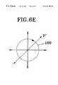
- FIGS. 5A to 5 Dillustrate a path of incident light when the reflective LCD of the present invention is off-state.
Landscapes
- Physics & Mathematics (AREA)
- Nonlinear Science (AREA)
- Mathematical Physics (AREA)
- Chemical & Material Sciences (AREA)
- Crystallography & Structural Chemistry (AREA)
- General Physics & Mathematics (AREA)
- Optics & Photonics (AREA)
- Geometry (AREA)
- Liquid Crystal (AREA)
- Engineering & Computer Science (AREA)
- Microelectronics & Electronic Packaging (AREA)
Abstract
Description
Claims (11)
Priority Applications (1)
| Application Number | Priority Date | Filing Date | Title |
|---|---|---|---|
| US10/015,082US6452658B1 (en) | 1998-08-24 | 2001-12-11 | Reflective LCD having high transmittance and method for manufacturing the same |
Applications Claiming Priority (2)
| Application Number | Priority Date | Filing Date | Title |
|---|---|---|---|
| KR98-34237 | 1998-08-24 | ||
| KR10-1998-0034237AKR100336886B1 (en) | 1998-08-24 | 1998-08-24 | Reflective liquid crystal display device with high opening rate and high transmittance and its manufacturing method |
Related Child Applications (1)
| Application Number | Title | Priority Date | Filing Date |
|---|---|---|---|
| US10/015,082DivisionUS6452658B1 (en) | 1998-08-24 | 2001-12-11 | Reflective LCD having high transmittance and method for manufacturing the same |
Publications (1)
| Publication Number | Publication Date |
|---|---|
| US6351300B1true US6351300B1 (en) | 2002-02-26 |
Family
ID=19548053
Family Applications (2)
| Application Number | Title | Priority Date | Filing Date |
|---|---|---|---|
| US09/379,452Expired - LifetimeUS6351300B1 (en) | 1998-08-24 | 1999-08-23 | Reflective LCD having high transmittance and method for manufacturing the same |
| US10/015,082Expired - LifetimeUS6452658B1 (en) | 1998-08-24 | 2001-12-11 | Reflective LCD having high transmittance and method for manufacturing the same |
Family Applications After (1)
| Application Number | Title | Priority Date | Filing Date |
|---|---|---|---|
| US10/015,082Expired - LifetimeUS6452658B1 (en) | 1998-08-24 | 2001-12-11 | Reflective LCD having high transmittance and method for manufacturing the same |
Country Status (2)
| Country | Link |
|---|---|
| US (2) | US6351300B1 (en) |
| KR (1) | KR100336886B1 (en) |
Cited By (14)
| Publication number | Priority date | Publication date | Assignee | Title |
|---|---|---|---|---|
| US6522380B2 (en)* | 1997-12-29 | 2003-02-18 | Hyundai Display Technology Inc. | Liquid crystal display having high transmittance and high aperture ratio |
| US6678027B2 (en)* | 2000-06-29 | 2004-01-13 | Boe-Hydis Technology Co., Ltd. | Fringe field switching mode LCD |
| US20040046919A1 (en)* | 2000-05-23 | 2004-03-11 | Ik-Soo Kim | In-plane switching LCD device |
| US20040196425A1 (en)* | 2003-04-04 | 2004-10-07 | Tsau-Hua Hsieh | IPS type liquid crystal display with protrusive electrodes |
| US20040212768A1 (en)* | 2003-04-25 | 2004-10-28 | Yang-En Wu | In-plane switching mode liquid crystal display |
| US20060139504A1 (en)* | 2004-12-24 | 2006-06-29 | Ahn Byung C | Liquid crystal display device and fabricating method thereof |
| US20060146245A1 (en)* | 2004-12-31 | 2006-07-06 | Ahn Byung C | Liquid crystal display device and fabricating method thereof |
| US20060146213A1 (en)* | 2004-12-31 | 2006-07-06 | Ahn Byung C | Liquid crystal display device and fabricating method thereof |
| CN1299154C (en)* | 2002-12-20 | 2007-02-07 | 西铁城电子股份有限公司 | Light conducting board and supporter for it |
| CN1322361C (en)* | 2003-04-18 | 2007-06-20 | 鸿富锦精密工业(深圳)有限公司 | Liquid crystal display device electric field with transverse |
| US20070206143A1 (en)* | 2003-06-02 | 2007-09-06 | Cambridge University Technical Services Limited | Liquid Crystal Devices |
| US20110043740A1 (en)* | 2000-07-13 | 2011-02-24 | Japan Science And Technology Corporation | Liquid crystal display device |
| US20140226097A1 (en)* | 2003-02-26 | 2014-08-14 | Compound Photonics Limited | Vertically aligned nematic mode liquid crystal display having large tilt angles and high contrast |
| US20180039143A1 (en)* | 2016-01-05 | 2018-02-08 | Shenzhen China Star Optoelectronics Technology Co. Ltd. | Liquid Crystal Display Panel, TFT Substrate And Manufacturing Method For The Same |
Families Citing this family (5)
| Publication number | Priority date | Publication date | Assignee | Title |
|---|---|---|---|---|
| KR100685936B1 (en)* | 2005-06-27 | 2007-02-22 | 엘지.필립스 엘시디 주식회사 | IPS mode liquid crystal display device and method of manufacturing the same |
| US20070212548A1 (en)* | 2006-03-10 | 2007-09-13 | Exatec Llc | Glazing system with high glass transition temperature decorative ink |
| JP5477523B2 (en)* | 2006-06-15 | 2014-04-23 | 三国電子有限会社 | Low cost large screen wide viewing angle fast response liquid crystal display |
| JP5238571B2 (en)* | 2009-03-25 | 2013-07-17 | 株式会社東芝 | Liquid crystal display |
| CN104157675A (en) | 2014-08-05 | 2014-11-19 | 京东方科技集团股份有限公司 | OLED (Organic Light Emitting Diode) display device and manufacturing method thereof as well as display device |
Citations (6)
| Publication number | Priority date | Publication date | Assignee | Title |
|---|---|---|---|---|
| JPH0850269A (en) | 1994-08-05 | 1996-02-20 | Toshiba Corp | Reflective liquid crystal display |
| US5548425A (en) | 1993-07-21 | 1996-08-20 | Sharp Kabushiki Kaisha | Reflective LCD having a resin-diffuser with dispersed metal oxide particles between a substrate and pixel electrodes or integral with the pixel electrodes |
| US5805247A (en)* | 1995-10-26 | 1998-09-08 | Hitachi, Ltd. | Liquid crystal display apparatus in which plural common electrodes are parallel to the pixel electrodes on the same substrate and a black matrix on the opposing substrate |
| US5831707A (en) | 1994-08-24 | 1998-11-03 | Hitachi, Ltd. | Active matrix type liquid crystal display apparatus |
| US6064460A (en)* | 1995-03-17 | 2000-05-16 | Hitachi, Ltd. | LCD with parallel field having counter electrode(s) at least equal to 1/2 width of video signal line |
| US6233034B1 (en)* | 1997-12-29 | 2001-05-15 | Hyundai Electronics Industries Co., Ltd. | Liquid crystal display and fabrication method |
Family Cites Families (3)
| Publication number | Priority date | Publication date | Assignee | Title |
|---|---|---|---|---|
| JPH0652344B2 (en)* | 1990-02-02 | 1994-07-06 | 株式会社リコー | Liquid crystal display |
| DE69327028T2 (en)* | 1992-09-25 | 2000-05-31 | Sony Corp., Tokio/Tokyo | Liquid crystal display device |
| US6181398B1 (en)* | 1998-09-03 | 2001-01-30 | International Business Machines Corporation | Multiple pixel driven mirror electrodes for improved aperture ratio of reflective displays |
- 1998
- 1998-08-24KRKR10-1998-0034237Apatent/KR100336886B1/ennot_activeExpired - Lifetime
- 1999
- 1999-08-23USUS09/379,452patent/US6351300B1/ennot_activeExpired - Lifetime
- 2001
- 2001-12-11USUS10/015,082patent/US6452658B1/ennot_activeExpired - Lifetime
Patent Citations (6)
| Publication number | Priority date | Publication date | Assignee | Title |
|---|---|---|---|---|
| US5548425A (en) | 1993-07-21 | 1996-08-20 | Sharp Kabushiki Kaisha | Reflective LCD having a resin-diffuser with dispersed metal oxide particles between a substrate and pixel electrodes or integral with the pixel electrodes |
| JPH0850269A (en) | 1994-08-05 | 1996-02-20 | Toshiba Corp | Reflective liquid crystal display |
| US5831707A (en) | 1994-08-24 | 1998-11-03 | Hitachi, Ltd. | Active matrix type liquid crystal display apparatus |
| US6064460A (en)* | 1995-03-17 | 2000-05-16 | Hitachi, Ltd. | LCD with parallel field having counter electrode(s) at least equal to 1/2 width of video signal line |
| US5805247A (en)* | 1995-10-26 | 1998-09-08 | Hitachi, Ltd. | Liquid crystal display apparatus in which plural common electrodes are parallel to the pixel electrodes on the same substrate and a black matrix on the opposing substrate |
| US6233034B1 (en)* | 1997-12-29 | 2001-05-15 | Hyundai Electronics Industries Co., Ltd. | Liquid crystal display and fabrication method |
Cited By (26)
| Publication number | Priority date | Publication date | Assignee | Title |
|---|---|---|---|---|
| US6522380B2 (en)* | 1997-12-29 | 2003-02-18 | Hyundai Display Technology Inc. | Liquid crystal display having high transmittance and high aperture ratio |
| US20040046919A1 (en)* | 2000-05-23 | 2004-03-11 | Ik-Soo Kim | In-plane switching LCD device |
| US7259821B2 (en)* | 2000-05-23 | 2007-08-21 | Lg. Philips Lcd Co., Ltd. | In-plane switching LCD device |
| US6678027B2 (en)* | 2000-06-29 | 2004-01-13 | Boe-Hydis Technology Co., Ltd. | Fringe field switching mode LCD |
| US20110043740A1 (en)* | 2000-07-13 | 2011-02-24 | Japan Science And Technology Corporation | Liquid crystal display device |
| US9007551B2 (en)* | 2000-07-13 | 2015-04-14 | Japan Science And Technology Agency | Liquid crystal display device |
| CN1299154C (en)* | 2002-12-20 | 2007-02-07 | 西铁城电子股份有限公司 | Light conducting board and supporter for it |
| US20140226097A1 (en)* | 2003-02-26 | 2014-08-14 | Compound Photonics Limited | Vertically aligned nematic mode liquid crystal display having large tilt angles and high contrast |
| US9551901B2 (en)* | 2003-02-26 | 2017-01-24 | Compound Photonics Limited | Vertically aligned nematic mode liquid crystal display having large tilt angles and high contrast |
| US20040196425A1 (en)* | 2003-04-04 | 2004-10-07 | Tsau-Hua Hsieh | IPS type liquid crystal display with protrusive electrodes |
| US7130011B2 (en)* | 2003-04-04 | 2006-10-31 | Innolux Display Corp. | IPS type liquid crystal display with protrusive electrodes |
| CN1322361C (en)* | 2003-04-18 | 2007-06-20 | 鸿富锦精密工业(深圳)有限公司 | Liquid crystal display device electric field with transverse |
| US6977706B2 (en)* | 2003-04-25 | 2005-12-20 | Au Optronics Corp. | In-plane switching mode liquid crystal display having heightened electrodes |
| US20040212768A1 (en)* | 2003-04-25 | 2004-10-28 | Yang-En Wu | In-plane switching mode liquid crystal display |
| US20070206143A1 (en)* | 2003-06-02 | 2007-09-06 | Cambridge University Technical Services Limited | Liquid Crystal Devices |
| US20060139504A1 (en)* | 2004-12-24 | 2006-06-29 | Ahn Byung C | Liquid crystal display device and fabricating method thereof |
| US20100231820A1 (en)* | 2004-12-24 | 2010-09-16 | Byung Chul Ahn | Liquid crystal display device and fabricating method thereof |
| US7751011B2 (en) | 2004-12-24 | 2010-07-06 | Lg Display Co., Ltd. | Method of fabricating a liquid crystal display device, comprising forming a protective film so that one end of the protective film is contacted with one end of the transparent conductive pattern. |
| US8013969B2 (en) | 2004-12-24 | 2011-09-06 | Lg Display Co., Ltd. | Liquid crystal display device comprising a protective film so that the protective film borders with one end of a transparent conductive pattern |
| US7760276B2 (en) | 2004-12-31 | 2010-07-20 | Lg Display Co., Ltd. | Liquid crystal display device and fabricating method thereof |
| US20100237349A1 (en)* | 2004-12-31 | 2010-09-23 | Byung Chul Ahn | Liquid crystal display device and fabricating method thereof |
| US8189162B2 (en) | 2004-12-31 | 2012-05-29 | Lg Display Co., Ltd. | Liquid crystal display device and fabricating method thereof |
| US7679699B2 (en) | 2004-12-31 | 2010-03-16 | Lg Display Co., Ltd. | Liquid crystal display device and fabricating method thereof |
| US20060146213A1 (en)* | 2004-12-31 | 2006-07-06 | Ahn Byung C | Liquid crystal display device and fabricating method thereof |
| US20060146245A1 (en)* | 2004-12-31 | 2006-07-06 | Ahn Byung C | Liquid crystal display device and fabricating method thereof |
| US20180039143A1 (en)* | 2016-01-05 | 2018-02-08 | Shenzhen China Star Optoelectronics Technology Co. Ltd. | Liquid Crystal Display Panel, TFT Substrate And Manufacturing Method For The Same |
Also Published As
| Publication number | Publication date |
|---|---|
| KR100336886B1 (en) | 2003-06-09 |
| US6452658B1 (en) | 2002-09-17 |
| US20020044248A1 (en) | 2002-04-18 |
| KR20000014693A (en) | 2000-03-15 |
Similar Documents
| Publication | Publication Date | Title |
|---|---|---|
| US6266118B1 (en) | Liquid crystal display of high aperture ratio and high transmittance having multi-domain having transparent conductive pixel and counter electrodes on the same substrate | |
| US6351300B1 (en) | Reflective LCD having high transmittance and method for manufacturing the same | |
| US6600542B2 (en) | Liquid crystal display having high transmittance and high aperture ratio in which the counter electrodes having rectangular plate shape and the pixel electrodes having branches | |
| US7995168B2 (en) | Transflective liquid crystal display having a relationship between the electrode spacing and cell gap in the reflection and transmission regions | |
| US6256081B1 (en) | LCD of high aperture ratio and high transmittance preventing color shift having transparent pixel and counter electrodes producing oblique electric fields | |
| US6646707B2 (en) | Fringe field switching mode LCD | |
| US20020008828A1 (en) | Fringe field switching mode LCD | |
| JPH11242233A (en) | Horizontal electric field type liquid crystal display device | |
| KR20080075064A (en) | Liquid crystal display and electronics | |
| JP2006317905A (en) | Transflective fringe field switching mode liquid crystal display device | |
| KR100325065B1 (en) | Reflective liquid crystal display with high brightness and wide viewing angle | |
| US6741311B1 (en) | Reflective type-fringe switching mode LCD having liquid crystal retardation (2n+1)λ/4 | |
| JP2009258332A (en) | Liquid crystal display device and electronic device | |
| US8035784B2 (en) | Semi-transmissive liquid crystal display device and manufacturing method of the same | |
| JP3807375B2 (en) | Liquid crystal display device and electronic device | |
| JP3901172B2 (en) | Liquid crystal display device and electronic device | |
| JP3549177B2 (en) | Liquid crystal display | |
| KR100685573B1 (en) | Liquid crystal display and electronic device | |
| US6320637B1 (en) | Liquid crystal display with wide viewing angle | |
| KR100674233B1 (en) | Fringe Field Drive Mode Liquid Crystal Display | |
| US20090244451A1 (en) | Liquid crystal display device and electronic apparatus | |
| JP2005128233A (en) | Liquid crystal display device and electronic device | |
| KR100290773B1 (en) | Reflective wide viewing angle lcd | |
| JP2008076503A (en) | Liquid crystal display | |
| JP6878265B2 (en) | Liquid crystal display device |
Legal Events
| Date | Code | Title | Description |
|---|---|---|---|
| AS | Assignment | Owner name:HYUNDAI ELECTRONICS INDUSTRIES CO., LTD., KOREA, R Free format text:ASSIGNMENT OF ASSIGNORS INTEREST;ASSIGNORS:PARK, IN CHEOL;LEE, SEUNG HEE;LEE, WON GEON;REEL/FRAME:010349/0500 Effective date:19991020 | |
| AS | Assignment | Owner name:HYNIX SEMICONDUCTOR INC., KOREA, REPUBLIC OF Free format text:CHANGE OF NAME;ASSIGNOR:HYUNDAI ELECTRONICS INDUSTRIES CO., LTD.;REEL/FRAME:012280/0141 Effective date:20010329 Owner name:HYUNDAI DISPLAY TECHNOLOGY INC., KOREA, REPUBLIC O Free format text:ASSIGNMENT OF ASSIGNORS INTEREST;ASSIGNOR:HYNIX SEMICONDUCTOR INC.;REEL/FRAME:012287/0925 Effective date:20011023 | |
| STCF | Information on status: patent grant | Free format text:PATENTED CASE | |
| AS | Assignment | Owner name:BOE-HYDIS TECHNOLOGY CO., LTD., KOREA, REPUBLIC OF Free format text:ASSIGNMENT OF ASSIGNORS INTEREST;ASSIGNOR:HYUNDAI DISPLAY TECHNOLOGY, INC.;REEL/FRAME:013879/0345 Effective date:20030303 | |
| FPAY | Fee payment | Year of fee payment:4 | |
| FPAY | Fee payment | Year of fee payment:8 | |
| FEPP | Fee payment procedure | Free format text:PAYOR NUMBER ASSIGNED (ORIGINAL EVENT CODE: ASPN); ENTITY STATUS OF PATENT OWNER: LARGE ENTITY | |
| FPAY | Fee payment | Year of fee payment:12 |