US6351067B2 - Organic electroluminescent device with improved hole injecting structure - Google Patents
Organic electroluminescent device with improved hole injecting structureDownload PDFInfo
- Publication number
- US6351067B2 US6351067B2US09/234,457US23445799AUS6351067B2US 6351067 B2US6351067 B2US 6351067B2US 23445799 AUS23445799 AUS 23445799AUS 6351067 B2US6351067 B2US 6351067B2
- Authority
- US
- United States
- Prior art keywords
- layer
- anode
- buffer layer
- organic electroluminescent
- cathode
- Prior art date
- Legal status (The legal status is an assumption and is not a legal conclusion. Google has not performed a legal analysis and makes no representation as to the accuracy of the status listed.)
- Expired - Lifetime
Links
- VYPSYNLAJGMNEJ-UHFFFAOYSA-NSilicium dioxideChemical compoundO=[Si]=OVYPSYNLAJGMNEJ-UHFFFAOYSA-N0.000claimsdescription22
- 238000000034methodMethods0.000claimsdescription14
- 239000000463materialSubstances0.000claimsdescription12
- 238000004519manufacturing processMethods0.000claimsdescription8
- 229920000553poly(phenylenevinylene)Polymers0.000claimsdescription6
- 229920000642polymerPolymers0.000claimsdescription5
- XLOMVQKBTHCTTD-UHFFFAOYSA-NZinc monoxideChemical compound[Zn]=OXLOMVQKBTHCTTD-UHFFFAOYSA-N0.000claimsdescription4
- 229910044991metal oxideInorganic materials0.000claimsdescription4
- 150000004706metal oxidesChemical class0.000claimsdescription4
- PBCFLUZVCVVTBY-UHFFFAOYSA-Ntantalum pentoxideInorganic materialsO=[Ta](=O)O[Ta](=O)=OPBCFLUZVCVVTBY-UHFFFAOYSA-N0.000claimsdescription4
- RUDFQVOCFDJEEF-UHFFFAOYSA-Nyttrium(III) oxideInorganic materials[O-2].[O-2].[O-2].[Y+3].[Y+3]RUDFQVOCFDJEEF-UHFFFAOYSA-N0.000claimsdescription4
- 230000008021depositionEffects0.000claimsdescription3
- AMGQUBHHOARCQH-UHFFFAOYSA-Nindium;oxotinChemical compound[In].[Sn]=OAMGQUBHHOARCQH-UHFFFAOYSA-N0.000claimsdescription3
- 230000005855radiationEffects0.000claimsdescription3
- 239000004065semiconductorSubstances0.000claimsdescription3
- GEQBRULPNIVQPP-UHFFFAOYSA-N2-[3,5-bis(1-phenylbenzimidazol-2-yl)phenyl]-1-phenylbenzimidazoleChemical compoundC1=CC=CC=C1N1C2=CC=CC=C2N=C1C1=CC(C=2N(C3=CC=CC=C3N=2)C=2C=CC=CC=2)=CC(C=2N(C3=CC=CC=C3N=2)C=2C=CC=CC=2)=C1GEQBRULPNIVQPP-UHFFFAOYSA-N0.000claimsdescription2
- GENZLHCFIPDZNJ-UHFFFAOYSA-N[In+3].[O-2].[Mg+2]Chemical compound[In+3].[O-2].[Mg+2]GENZLHCFIPDZNJ-UHFFFAOYSA-N0.000claimsdescription2
- BEQNOZDXPONEMR-UHFFFAOYSA-Ncadmium;oxotinChemical compound[Cd].[Sn]=OBEQNOZDXPONEMR-UHFFFAOYSA-N0.000claimsdescription2
- 230000008020evaporationEffects0.000claimsdescription2
- 238000001704evaporationMethods0.000claimsdescription2
- -1poly (paraphenylene vinylene)Polymers0.000claimsdescription2
- 229910052814silicon oxideInorganic materials0.000claimsdescription2
- XOLBLPGZBRYERU-UHFFFAOYSA-Ntin dioxideChemical compoundO=[Sn]=OXOLBLPGZBRYERU-UHFFFAOYSA-N0.000claimsdescription2
- 229910001887tin oxideInorganic materials0.000claimsdescription2
- 239000011787zinc oxideSubstances0.000claimsdescription2
- 238000000151depositionMethods0.000claims2
- 239000010410layerSubstances0.000description65
- 229910052681coesiteInorganic materials0.000description10
- 229910052906cristobaliteInorganic materials0.000description10
- 239000000377silicon dioxideSubstances0.000description10
- 229910052682stishoviteInorganic materials0.000description10
- 229910052905tridymiteInorganic materials0.000description10
- 229910052751metalInorganic materials0.000description5
- 239000002184metalSubstances0.000description5
- 238000002347injectionMethods0.000description4
- 239000007924injectionSubstances0.000description4
- 239000012044organic layerSubstances0.000description4
- 239000000758substrateSubstances0.000description4
- 229910010272inorganic materialInorganic materials0.000description3
- 239000011147inorganic materialSubstances0.000description3
- CSCPPACGZOOCGX-UHFFFAOYSA-NAcetoneChemical compoundCC(C)=OCSCPPACGZOOCGX-UHFFFAOYSA-N0.000description2
- IJGRMHOSHXDMSA-UHFFFAOYSA-NAtomic nitrogenChemical compoundN#NIJGRMHOSHXDMSA-UHFFFAOYSA-N0.000description2
- OKTJSMMVPCPJKN-UHFFFAOYSA-NCarbonChemical compound[C]OKTJSMMVPCPJKN-UHFFFAOYSA-N0.000description2
- LFQSCWFLJHTTHZ-UHFFFAOYSA-NEthanolChemical compoundCCOLFQSCWFLJHTTHZ-UHFFFAOYSA-N0.000description2
- 229910052783alkali metalInorganic materials0.000description2
- 150000001340alkali metalsChemical class0.000description2
- 125000003118aryl groupChemical group0.000description2
- 230000004888barrier functionEffects0.000description2
- 229910052799carbonInorganic materials0.000description2
- 239000010406cathode materialSubstances0.000description2
- 239000002800charge carrierSubstances0.000description2
- 238000005260corrosionMethods0.000description2
- 230000007797corrosionEffects0.000description2
- 239000011521glassSubstances0.000description2
- 150000002739metalsChemical class0.000description2
- 239000000203mixtureSubstances0.000description2
- 229910052757nitrogenInorganic materials0.000description2
- 150000003512tertiary aminesChemical class0.000description2
- 239000010409thin filmSubstances0.000description2
- CBENFWSGALASAD-UHFFFAOYSA-NOzoneChemical compound[O-][O+]=OCBENFWSGALASAD-UHFFFAOYSA-N0.000description1
- 239000002131composite materialSubstances0.000description1
- 239000004020conductorSubstances0.000description1
- 238000010276constructionMethods0.000description1
- 238000011109contaminationMethods0.000description1
- 239000008367deionised waterSubstances0.000description1
- 229910021641deionized waterInorganic materials0.000description1
- 239000003599detergentSubstances0.000description1
- 238000010586diagramMethods0.000description1
- 238000005401electroluminescenceMethods0.000description1
- 238000004020luminiscence typeMethods0.000description1
- 230000003287optical effectEffects0.000description1
- 239000003960organic solventSubstances0.000description1
- 238000005215recombinationMethods0.000description1
- 230000006798recombinationEffects0.000description1
- 229910052709silverInorganic materials0.000description1
- 239000002356single layerSubstances0.000description1
- 229910052715tantalumInorganic materials0.000description1
- GUVRBAGPIYLISA-UHFFFAOYSA-Ntantalum atomChemical compound[Ta]GUVRBAGPIYLISA-UHFFFAOYSA-N0.000description1
- XLYOFNOQVPJJNP-UHFFFAOYSA-NwaterChemical compoundOXLYOFNOQVPJJNP-UHFFFAOYSA-N0.000description1
Images

Classifications
- H—ELECTRICITY
- H10—SEMICONDUCTOR DEVICES; ELECTRIC SOLID-STATE DEVICES NOT OTHERWISE PROVIDED FOR
- H10K—ORGANIC ELECTRIC SOLID-STATE DEVICES
- H10K50/00—Organic light-emitting devices
- H10K50/10—OLEDs or polymer light-emitting diodes [PLED]
- H10K50/17—Carrier injection layers
- H—ELECTRICITY
- H10—SEMICONDUCTOR DEVICES; ELECTRIC SOLID-STATE DEVICES NOT OTHERWISE PROVIDED FOR
- H10K—ORGANIC ELECTRIC SOLID-STATE DEVICES
- H10K50/00—Organic light-emitting devices
- H10K50/10—OLEDs or polymer light-emitting diodes [PLED]
- H10K50/17—Carrier injection layers
- H10K50/171—Electron injection layers
- Y—GENERAL TAGGING OF NEW TECHNOLOGICAL DEVELOPMENTS; GENERAL TAGGING OF CROSS-SECTIONAL TECHNOLOGIES SPANNING OVER SEVERAL SECTIONS OF THE IPC; TECHNICAL SUBJECTS COVERED BY FORMER USPC CROSS-REFERENCE ART COLLECTIONS [XRACs] AND DIGESTS
- Y10—TECHNICAL SUBJECTS COVERED BY FORMER USPC
- Y10S—TECHNICAL SUBJECTS COVERED BY FORMER USPC CROSS-REFERENCE ART COLLECTIONS [XRACs] AND DIGESTS
- Y10S428/00—Stock material or miscellaneous articles
- Y10S428/917—Electroluminescent
Definitions
- the present inventionpertains to organic thin-film electroluminescent devices and a method of manufacture of such devices.
- OELDsorganic electroluminescent devices
- Representatives of early OELDsare U.S. Pat. No. 3,172,862 to Gurnee et al, issued Mar. 9, 1965; U.S. Pat. No. 3,173,050 to Gurnee, issued Mar. 9, 1965; and U.S. Pat. No. 3,710,167 to Dresner, issued Jan. 9, 1973.
- These devicescomprised a single organic emitting layer having thicknesses above 1 mm and two electrodes (cathode and anode). Alkali metals were used as the cathode materials as they had the lowest work function values.
- U.S. Pat. No. 4,356,429 to Tang et aldisclosed an OELD with two organic layers, in which the organic luminescent medium consisted of two extremely thin layers separating the anode and the cathode. These comprised one layer injecting and transporting holes and the other layer injecting and transporting electrons and also acting as the organic luminescent zone of the device.
- U.S. Pat. No. 4,885,211 to Tang et aldisclosed an OELD with its cathode comprising a layer of a plurality of metals other than single alkali metals, at least one of the metals having a work function of less than 4 eV.
- U.S. Pat. No. 5,608,287 to Hung et al.disclosed OELDs having a conductive electron injector.
- 5,668,438 to Shi et aldisclosed an OELD in which the materials making up the electron transporting layer (ETL) and the hole transporting layer (HTL) were selected so that the energy barrier for hole injection from the HTL to the ETL was substantially higher than the energy barrier for electron injection from the ETL to the HTL. In that case, light was emitted from the HTL rather than the ETL.
- ETLelectron transporting layer
- HTLhole transporting layer
- U.S. Pat. No. 5,776,623 to Hung et aldisclosed an OELD containing a transparent electron-injecting electrode.
- the electrodeincluded a thin non-conductive layer contacting the electroluminescent layer and a conductive transparent overcoat layer. The thickness of the nonconductive layer was selected so that the bilayer acted as an electron injecting contact and provided stability against atmospheric corrosion.
- U.S. Pat. No. 5,061,569 to Vanslyke et aldisclosed an internal junction OELD in which the hole injecting and transporting zone included a tertiary amine containing at least two tertiary amine moieties and including, attached to a tertiary amine nitrogen atom, an aromatic moiety containing at least two fused aromatic rings.
- U.S. Pat. No. 5,783,292 to Tokito et aldisclosed an OELD in which organic-inorganic composite thin film was used.
- This inventioncomprises an OELD and method of manufacture in which an inorganic buffer layer is included in the hole injecting region.
- the devicecomprises in order: an ITO-covered glass substrate which behaves as the hole injector and is transparent and transmissive to optical radiation, a layer of inorganic material as a buffer to the hole injection, an organic single layer or multilayer structure for electroluminescence and carrier confinement, and a layer of low-work-function material as an electron injector which is stable relative to atmospheric corrosion.
- the buffer layermay also be included in the electron injecting region.
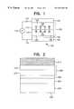
- FIGS. 1 and 2which are schematic diagrams of an embodiment of the OELD of the invention
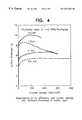
- FIG. 3is a graphical representation of the results of different thickness of buffer layer in terms of brightness.
- FIG. 4is a graphical representation of the results of FIG. 3 in terms of electroluminescent efficiency.
- An electroluminescent (EL) device 100 of the inventionis schematically illustrated in FIG. 1 .
- Anode 102is separated from cathode 104 by an inorganic buffer layer 106 and an organic luminescent medium 108 , which, as shown in this embodiment, consists of two superimposed layers.
- Layer 110which is located above the buffer layer 106 , forms a hole injecting zone of the organic luminescent medium.
- layer 112which forms an electron transporting zone of the organic luminescent medium.
- the anode and the cathodeare connected to an external AC or DC power source 114 by conductors 116 and 118 , respectively.
- the power sourcecan be pulsed or continuous wave.
- the EL device 100When the EL device 100 is forward biased, i.e., the potential of the anode is higher than that of the cathode, there occurs injection of holes (positive charge carriers) into the lower organic layer, as schematically shown at 120 , while electrons are injected into the upper organic layer, as schematically shown at 122 , in the luminescent medium.
- the injected holes and electronseach migrate toward the oppositely charged electrode, as shown by the arrows 124 and 126 , respectively. This results in hole-electron recombination.
- a migrating electrondrops from its conduction potential to a valence band in filing a hole, energy is released as light.
- the organic luminescent mediumforms between the electrodes a luminescent zone receiving mobile charge carriers from each electrode.
- the released lightcan be emitted from the organic luminescent material through one or more edges 128 of the organic luminescent medium separating the electrodes, through the anode, through the cathode, or through any combination of the foregoing.
- Organic EL device 200 shown in FIG. 2is illustrative of one preferred embodiment of the invention. Same as in previous OELDs' fabrication, a transparent anode electrode is used in the present invention.
- Layer 202is a transparent and insulating support onto which is deposited a conductive and light transmissive electrode 204 . Typically, this layer is made from metal or metal oxide such as ITO.
- This layeras an anode electrode, possesses a relatively high work function.
- Adjacent to 204is the anode-combined buffer layer 206 , which, in this embodiment, is selected from the group consisting of SiO x , Y 2 O 3 , and Ta 2 O 5 , where x is from 1 to 2.
- the organic luminescent medium 208consisting of hole injecting zone 210 and electron transporting zone 212 in which luminescence occurs.
- the top electrode 214acts as the electron injector with a relatively low work function. It is usually either a single metal or a multi-metal mixture formed by codeposition in vacuum.
- the preferred embodiments abovedescribe an OELD which positions the buffer layer between the anode and the luminescent medium.
- the buffer layermay also increase efficiency when positioned between the cathode and the luminescent medium, for example, between the cathode and electron transporting layer.
- multiple buffer layerssuch as a buffer layer adjacent the anode and a further buffer layer adjacent the cathode are possible. There is no requirement for identical buffer layers in such a multi-layer structure with the buffer layers on opposed sides of the luminescent medium able to be of different materials or mixtures as required.
- the buffer layers describedhave been selected from a particular group of oxides.
- the buffer layeris chosen from insulating metal oxides, semiconductor oxides, diamond-like carbon and nitrogen doped carbon.
- insulating metal oxidessemiconductor oxides
- diamond-like carbondiamond-like carbon
- nitrogen doped carbona number of different materials may be used in the buffer layer to perform the same function. The list provided is not considered exhaustive.
- the electroluminescent element contained within the devicecan comprise variety of materials found suitable for such purposes. These include the inclusion of molecules selected from Alq, TPD, NPB and TPBI as well as a variety of polymers.
- the polymersmay include such polymers as poly (paraphenylene vinylene) (PPV), PPV copolymers and derivatives. Again, this is not an exhaustive list of possible materials for this element.
- the anodecan be made from many suitable materials for the purpose.
- suitable materialsfor the purpose.
- Typically such anodesare made from transparent conducting oxides. These include indium-tin-oxide, aluminum- or indium-doped zinc oxide, tin oxide, magnesium-indium-oxide and cadmium-tin-oxide.
- the device structurehas an inorganic buffer layer and a two organic-layer stack, namely hole transporting layer and fluorescent emitting and electron transporting layer.
- An indium-tin-oxide coated glass substratewas sequentially ultrasonicated in a commercial detergent, rinsed in deionized water, degreased in organic solvent, such as ethanol and acetone, and exposed to ultraviolet light and ozone for a few minutes.
- An inorganic buffer layer (0-200 Angstroms)was then deposited on top of the ITO coated substrate by evaporation.
- a fluorescent emitting and electron transporting layer of Alq(600 Angstroms) was then deposited onto the hole transporting layer.
- the above sequencecompleted the deposition of the OELD.
- the devicewas then packaged in a dry glove box for protection against ambient environment.
- the OELDswere fabricated according to the procedure of Example 1.
- the buffer layers with different thicknesses of SiO 2were used.
- Table 1lists the EL luminance quantum efficiency measured in unit of candela per ampere, and luminance output under a constant current bias of 20 mA/cm 2 .
- the luminance efficiencyit can be observed that there may be a reduction in efficiency with a particularly thin layer.
- the efficiencyincreases towards the thickness of 1 nm. There may then be a tailing off of efficiency as the thickness increases.
- This particular buffer layeris an insulating layer and will inhibit current as the layer thickness increases.
- the thickness as provided in this tableshows the performance of SiO 2 . Different thicknesses may provide different results with alternative materials used as the buffer layer.
- FIG. 3shows the B-I-V curves of four devices with different thicknesses of buffer layer (SiO 2 ).
- FIG. 4shows the electroluminescent efficiency of the four devices with different thicknesses of buffer layer (SiO 2 ).
- the OELDswere fabricated according to the procedure of Example 1. Buffer layers made of different inorganic materials, such as SiO 2 , Y 2 O 3 and Ta 2 O 5 were used. Table 2 lists the EL luminance quantum efficiency measured in unit of candela per ampere and luminance output under a constant current bias of 20 mA/cm 2 (the thickness of the inorganic materials is about 1.0 nm).
- the OELDswere fabricated according to the procedure of Example 1.
- the substrate with buffer layerwas further treated by radiation, which effectively protects the surface of the buffer layer against harmful contamination. Even higher EL efficiency can be obtained thereby.
- the fabrication procedure provided in the examplesagain discloses a method of manufacturing an OELD which incorporates a buffer layer between the cathode and anode.
- the examples givendeposit the buffer layer onto the intended anode of the device. Again, it should be noted that the layer may be deposited prior to deposition of the cathode or onto the cathode be the device is deposited in reverse. The order of the layers in the examples are for these preferred embodiments only.
Landscapes
- Physics & Mathematics (AREA)
- Optics & Photonics (AREA)
- Electroluminescent Light Sources (AREA)
Abstract
Description
| TABLE 1 | ||||||
| SiO2Thickness (nm) | 0 | 0.5 | 1.0 | 1.5 | ||
| CIEx | 0.334 | 0.338 | 0.339 | 0.339 | ||
| CIEy | 0.562 | 0.563 | 0.562 | 0.562 | ||
| Luminance | 1,140 | 960 | 1,820 | 1,680 | ||
| Luminance Eff. (cd/A) | 5.7 | 4.8 | 9.1 | 8.4 | ||
| TABLE 2 | |||||
| Materials | SiO2 | Y2O3 | Ta2O5 | ||
| CIEx | 0.339 | 0.334 | 0.335 | ||
| CIEy | 0.562 | 0.562 | 0.562 | ||
| Luminance | 1,820 | 1,280 | 1,360 | ||
| Luminance Eff. (cd/A) | 9.1 | 6.4 | 6.8 | ||
Claims (19)
Priority Applications (1)
| Application Number | Priority Date | Filing Date | Title |
|---|---|---|---|
| US09/234,457US6351067B2 (en) | 1999-01-21 | 1999-01-21 | Organic electroluminescent device with improved hole injecting structure |
Applications Claiming Priority (1)
| Application Number | Priority Date | Filing Date | Title |
|---|---|---|---|
| US09/234,457US6351067B2 (en) | 1999-01-21 | 1999-01-21 | Organic electroluminescent device with improved hole injecting structure |
Publications (2)
| Publication Number | Publication Date |
|---|---|
| US20020011782A1 US20020011782A1 (en) | 2002-01-31 |
| US6351067B2true US6351067B2 (en) | 2002-02-26 |
Family
ID=22881476
Family Applications (1)
| Application Number | Title | Priority Date | Filing Date |
|---|---|---|---|
| US09/234,457Expired - LifetimeUS6351067B2 (en) | 1999-01-21 | 1999-01-21 | Organic electroluminescent device with improved hole injecting structure |
Country Status (1)
| Country | Link |
|---|---|
| US (1) | US6351067B2 (en) |
Cited By (18)
| Publication number | Priority date | Publication date | Assignee | Title |
|---|---|---|---|---|
| US20030080338A1 (en)* | 2001-10-26 | 2003-05-01 | Semiconductor Energy Laboratory Co., Ltd. | Light emitting device |
| US20040108810A1 (en)* | 2002-09-26 | 2004-06-10 | Chi Mei Optoelectronics Corp. | Organic light-emitting device, organic light-emitting display apparatus, and method of manufacturing organic light-emitting display apparatus |
| US20040201346A1 (en)* | 2003-04-10 | 2004-10-14 | Jui-Fen Pai | Organic light-emitting display having anti-reflective and inert cathode |
| US20040245917A1 (en)* | 2003-04-23 | 2004-12-09 | Zheng-Hong Lu | Light-emitting devices with an embedded charge injection electrode |
| US20050009350A1 (en)* | 2003-07-08 | 2005-01-13 | Mirko Vogt | Carbon hard mask with bonding layer for bonding to metal |
| US20060066226A1 (en)* | 1999-04-30 | 2006-03-30 | Idemitsu Kosan Co., Ltd. | Organic electroluminescence element and manufacturing method thereof |
| US20060087230A1 (en)* | 2004-10-22 | 2006-04-27 | Eastman Kodak Company | Desiccant film in top-emitting OLED |
| US20060240280A1 (en)* | 2005-04-21 | 2006-10-26 | Eastman Kodak Company | OLED anode modification layer |
| US20060243329A1 (en)* | 2005-04-29 | 2006-11-02 | Ti Group Automotive Systems, L.L.C. | Check valve apparatus for fuel delivery systems |
| US20060251918A1 (en)* | 2003-12-11 | 2006-11-09 | Toshihiro Iwakuma | Organic electroluminescent device material and organic electroluminescent device using same |
| US20070102698A1 (en)* | 1999-12-31 | 2007-05-10 | Kang Min S | Organic electronic device |
| US20080231179A1 (en)* | 2007-03-23 | 2008-09-25 | Toppan Printing Co., Ltd. | Organic Electroluminescence Element and Display Using the Same |
| US20080309234A1 (en)* | 2007-06-15 | 2008-12-18 | Samsung Electronics Co., Ltd. | Alternating current driving type quantum dot electroluminescent device |
| US20090009101A1 (en)* | 2006-01-18 | 2009-01-08 | Kang Min-Soo | Oled Having Stacked Organic Light-Emitting Units |
| US20090091242A1 (en)* | 2007-10-05 | 2009-04-09 | Liang-Sheng Liao | Hole-injecting layer in oleds |
| CN100570924C (en)* | 2005-12-05 | 2009-12-16 | 中华映管股份有限公司 | Method for manufacturing organic electroluminescent element and method for manufacturing carbon-rich thin film |
| US9911934B2 (en)* | 2016-02-01 | 2018-03-06 | Osram Oled Gmbh | OLED and method for producing an OLED |
| WO2019147479A1 (en) | 2018-01-25 | 2019-08-01 | OLEDWorks LLC | Method for mask-free oled deposition and manufacture |
Families Citing this family (11)
| Publication number | Priority date | Publication date | Assignee | Title |
|---|---|---|---|---|
| KR100377321B1 (en)* | 1999-12-31 | 2003-03-26 | 주식회사 엘지화학 | Electronic device comprising organic compound having p-type semiconducting characteristics |
| US7560175B2 (en)* | 1999-12-31 | 2009-07-14 | Lg Chem, Ltd. | Electroluminescent devices with low work function anode |
| JP3895938B2 (en)* | 2001-03-22 | 2007-03-22 | 三洋電機株式会社 | Organic electroluminescence device and method for manufacturing the same |
| KR100718765B1 (en)* | 2004-08-19 | 2007-05-15 | 주식회사 엘지화학 | Organic electroluminescent divice comprising a buffer layer and method for fabricating the same |
| US7759856B2 (en)* | 2004-12-17 | 2010-07-20 | Honeywell International Inc. | Organic light emitting diode (OLED) having improved stability, luminance, and efficiency |
| KR100890862B1 (en)* | 2005-11-07 | 2009-03-27 | 주식회사 엘지화학 | Organic electroluminescent device and method for preparing the same |
| KR100792139B1 (en)* | 2006-02-06 | 2008-01-04 | 주식회사 엘지화학 | Organic light emitting device using inorganic insulating layer as electron injection layer and method for manufacturing same |
| KR100897762B1 (en)* | 2007-04-07 | 2009-05-15 | 김용성 | Organic light emitting device using zinc oxide transparent conductive film |
| CN102626002B (en)* | 2009-08-07 | 2015-09-09 | 三井金属矿业株式会社 | For the anode construction body of organic EL element, its production method and organic EL element |
| US9391124B2 (en) | 2013-07-02 | 2016-07-12 | Samsung Display Co., Ltd. | Organic light emitting diode display |
| US20150008394A1 (en)* | 2013-07-02 | 2015-01-08 | Samsung Display Co., Ltd. | Organic light emitting diode display |
Citations (19)
| Publication number | Priority date | Publication date | Assignee | Title |
|---|---|---|---|---|
| US3173050A (en) | 1962-09-19 | 1965-03-09 | Dow Chemical Co | Electroluminescent cell |
| US3172862A (en) | 1960-09-29 | 1965-03-09 | Dow Chemical Co | Organic electroluminescent phosphors |
| US3710167A (en) | 1970-07-02 | 1973-01-09 | Rca Corp | Organic electroluminescent cells having a tunnel injection cathode |
| US4356429A (en) | 1980-07-17 | 1982-10-26 | Eastman Kodak Company | Organic electroluminescent cell |
| US4757235A (en)* | 1985-04-30 | 1988-07-12 | Nec Corporation | Electroluminescent device with monolithic substrate |
| US4885211A (en) | 1987-02-11 | 1989-12-05 | Eastman Kodak Company | Electroluminescent device with improved cathode |
| US5061569A (en) | 1990-07-26 | 1991-10-29 | Eastman Kodak Company | Electroluminescent device with organic electroluminescent medium |
| US5317169A (en)* | 1990-02-23 | 1994-05-31 | Sumitomo Chemical Company, Limited | Organic electroluminescence device |
| US5530269A (en)* | 1993-11-18 | 1996-06-25 | Eastman Kodak Company | Light emitting device comprising an organic led array on an ultra thin substrate |
| US5608287A (en) | 1995-02-23 | 1997-03-04 | Eastman Kodak Company | Conductive electron injector for light-emitting diodes |
| US5668438A (en) | 1996-06-06 | 1997-09-16 | Motorola | Organic electroluminescent device with emission from hole transporting layer |
| US5734225A (en)* | 1996-07-10 | 1998-03-31 | International Business Machines Corporation | Encapsulation of organic light emitting devices using siloxane or siloxane derivatives |
| US5741626A (en)* | 1996-04-15 | 1998-04-21 | Motorola, Inc. | Method for forming a dielectric tantalum nitride layer as an anti-reflective coating (ARC) |
| US5776623A (en) | 1996-07-29 | 1998-07-07 | Eastman Kodak Company | Transparent electron-injecting electrode for use in an electroluminescent device |
| US5783292A (en) | 1994-09-29 | 1998-07-21 | Kabushiki Kaisha Toyota Chuo Kenkyusho | Electroluminescent device with organic-inorganic composite thin film |
| US5932964A (en)* | 1996-09-24 | 1999-08-03 | Mccann & Associates, Inc. | Europium-containing group IIA fluoride epitaxial layer on silicon |
| US5969474A (en)* | 1996-10-24 | 1999-10-19 | Tdk Corporation | Organic light-emitting device with light transmissive anode and light transmissive cathode including zinc-doped indium oxide |
| US6067222A (en)* | 1998-11-25 | 2000-05-23 | Applied Materials, Inc. | Substrate support apparatus and method for fabricating same |
| US6140763A (en)* | 1998-07-28 | 2000-10-31 | Eastman Kodak Company | Interfacial electron-injecting layer formed from a doped cathode for organic light-emitting structure |
- 1999
- 1999-01-21USUS09/234,457patent/US6351067B2/ennot_activeExpired - Lifetime
Patent Citations (19)
| Publication number | Priority date | Publication date | Assignee | Title |
|---|---|---|---|---|
| US3172862A (en) | 1960-09-29 | 1965-03-09 | Dow Chemical Co | Organic electroluminescent phosphors |
| US3173050A (en) | 1962-09-19 | 1965-03-09 | Dow Chemical Co | Electroluminescent cell |
| US3710167A (en) | 1970-07-02 | 1973-01-09 | Rca Corp | Organic electroluminescent cells having a tunnel injection cathode |
| US4356429A (en) | 1980-07-17 | 1982-10-26 | Eastman Kodak Company | Organic electroluminescent cell |
| US4757235A (en)* | 1985-04-30 | 1988-07-12 | Nec Corporation | Electroluminescent device with monolithic substrate |
| US4885211A (en) | 1987-02-11 | 1989-12-05 | Eastman Kodak Company | Electroluminescent device with improved cathode |
| US5317169A (en)* | 1990-02-23 | 1994-05-31 | Sumitomo Chemical Company, Limited | Organic electroluminescence device |
| US5061569A (en) | 1990-07-26 | 1991-10-29 | Eastman Kodak Company | Electroluminescent device with organic electroluminescent medium |
| US5530269A (en)* | 1993-11-18 | 1996-06-25 | Eastman Kodak Company | Light emitting device comprising an organic led array on an ultra thin substrate |
| US5783292A (en) | 1994-09-29 | 1998-07-21 | Kabushiki Kaisha Toyota Chuo Kenkyusho | Electroluminescent device with organic-inorganic composite thin film |
| US5608287A (en) | 1995-02-23 | 1997-03-04 | Eastman Kodak Company | Conductive electron injector for light-emitting diodes |
| US5741626A (en)* | 1996-04-15 | 1998-04-21 | Motorola, Inc. | Method for forming a dielectric tantalum nitride layer as an anti-reflective coating (ARC) |
| US5668438A (en) | 1996-06-06 | 1997-09-16 | Motorola | Organic electroluminescent device with emission from hole transporting layer |
| US5734225A (en)* | 1996-07-10 | 1998-03-31 | International Business Machines Corporation | Encapsulation of organic light emitting devices using siloxane or siloxane derivatives |
| US5776623A (en) | 1996-07-29 | 1998-07-07 | Eastman Kodak Company | Transparent electron-injecting electrode for use in an electroluminescent device |
| US5932964A (en)* | 1996-09-24 | 1999-08-03 | Mccann & Associates, Inc. | Europium-containing group IIA fluoride epitaxial layer on silicon |
| US5969474A (en)* | 1996-10-24 | 1999-10-19 | Tdk Corporation | Organic light-emitting device with light transmissive anode and light transmissive cathode including zinc-doped indium oxide |
| US6140763A (en)* | 1998-07-28 | 2000-10-31 | Eastman Kodak Company | Interfacial electron-injecting layer formed from a doped cathode for organic light-emitting structure |
| US6067222A (en)* | 1998-11-25 | 2000-05-23 | Applied Materials, Inc. | Substrate support apparatus and method for fabricating same |
Cited By (30)
| Publication number | Priority date | Publication date | Assignee | Title |
|---|---|---|---|---|
| US7423371B2 (en)* | 1999-04-30 | 2008-09-09 | Idemitsu Kosan Co., Ltd. | Organic electroluminescence element and manufacturing method thereof |
| US20060066226A1 (en)* | 1999-04-30 | 2006-03-30 | Idemitsu Kosan Co., Ltd. | Organic electroluminescence element and manufacturing method thereof |
| US20070102698A1 (en)* | 1999-12-31 | 2007-05-10 | Kang Min S | Organic electronic device |
| US8253126B2 (en) | 1999-12-31 | 2012-08-28 | Lg Chem. Ltd. | Organic electronic device |
| US20100117063A9 (en)* | 1999-12-31 | 2010-05-13 | Kang Min Soo | Organic electronic device |
| US7488986B2 (en) | 2001-10-26 | 2009-02-10 | Semiconductor Energy Laboratory Co., Ltd. | Light emitting device |
| US20030080338A1 (en)* | 2001-10-26 | 2003-05-01 | Semiconductor Energy Laboratory Co., Ltd. | Light emitting device |
| US20040108810A1 (en)* | 2002-09-26 | 2004-06-10 | Chi Mei Optoelectronics Corp. | Organic light-emitting device, organic light-emitting display apparatus, and method of manufacturing organic light-emitting display apparatus |
| CN100367530C (en)* | 2002-09-26 | 2008-02-06 | 奇美电子股份有限公司 | Image display device, organic electroluminescent element, and method for manufacturing image display device |
| US20060017378A1 (en)* | 2002-09-26 | 2006-01-26 | Chi Mei Optoelectronics Corp. | Organic light-emitting device, organic light-emitting display apparatus, and method of manufacturing organic light-emitting display apparatus |
| US7182663B2 (en)* | 2002-09-26 | 2007-02-27 | Chi Mei Optoelectronics Corp. | Method of manufacturing an organic light-emitting display apparatus having a diamond-like carbon film in contact wiring |
| US7176620B2 (en)* | 2002-09-26 | 2007-02-13 | Chi Mei Optoelectronics Corp. | Organic light-emitting device, organic light-emitting display apparatus, and method of manufacturing organic light-emitting display apparatus |
| US7176618B2 (en)* | 2003-04-10 | 2007-02-13 | Tpo Displays Corp. | Organic light-emitting display having anti-reflective and inert cathode |
| US20040201346A1 (en)* | 2003-04-10 | 2004-10-14 | Jui-Fen Pai | Organic light-emitting display having anti-reflective and inert cathode |
| US20040245917A1 (en)* | 2003-04-23 | 2004-12-09 | Zheng-Hong Lu | Light-emitting devices with an embedded charge injection electrode |
| US20050009350A1 (en)* | 2003-07-08 | 2005-01-13 | Mirko Vogt | Carbon hard mask with bonding layer for bonding to metal |
| US20060251918A1 (en)* | 2003-12-11 | 2006-11-09 | Toshihiro Iwakuma | Organic electroluminescent device material and organic electroluminescent device using same |
| US20060087230A1 (en)* | 2004-10-22 | 2006-04-27 | Eastman Kodak Company | Desiccant film in top-emitting OLED |
| US20060240280A1 (en)* | 2005-04-21 | 2006-10-26 | Eastman Kodak Company | OLED anode modification layer |
| US20060243329A1 (en)* | 2005-04-29 | 2006-11-02 | Ti Group Automotive Systems, L.L.C. | Check valve apparatus for fuel delivery systems |
| CN100570924C (en)* | 2005-12-05 | 2009-12-16 | 中华映管股份有限公司 | Method for manufacturing organic electroluminescent element and method for manufacturing carbon-rich thin film |
| US20090009101A1 (en)* | 2006-01-18 | 2009-01-08 | Kang Min-Soo | Oled Having Stacked Organic Light-Emitting Units |
| US8680693B2 (en) | 2006-01-18 | 2014-03-25 | Lg Chem. Ltd. | OLED having stacked organic light-emitting units |
| US20080231179A1 (en)* | 2007-03-23 | 2008-09-25 | Toppan Printing Co., Ltd. | Organic Electroluminescence Element and Display Using the Same |
| US7723916B2 (en)* | 2007-03-23 | 2010-05-25 | Toppan Printing Co., Ltd. | Organic electroluminescence element and display using the same |
| US20080309234A1 (en)* | 2007-06-15 | 2008-12-18 | Samsung Electronics Co., Ltd. | Alternating current driving type quantum dot electroluminescent device |
| US20090091242A1 (en)* | 2007-10-05 | 2009-04-09 | Liang-Sheng Liao | Hole-injecting layer in oleds |
| US9911934B2 (en)* | 2016-02-01 | 2018-03-06 | Osram Oled Gmbh | OLED and method for producing an OLED |
| WO2019147479A1 (en) | 2018-01-25 | 2019-08-01 | OLEDWorks LLC | Method for mask-free oled deposition and manufacture |
| US10923689B2 (en) | 2018-01-25 | 2021-02-16 | OLEDWorks LLC | Method for mask-free OLED deposition and manufacture |
Also Published As
| Publication number | Publication date |
|---|---|
| US20020011782A1 (en) | 2002-01-31 |
Similar Documents
| Publication | Publication Date | Title |
|---|---|---|
| US6351067B2 (en) | Organic electroluminescent device with improved hole injecting structure | |
| US6208077B1 (en) | Organic electroluminescent device with a non-conductive fluorocarbon polymer layer | |
| US6392250B1 (en) | Organic light emitting devices having improved performance | |
| JP3327558B2 (en) | Organic / inorganic alloys used to improve organic electroluminescent devices | |
| US6278236B1 (en) | Organic electroluminescent devices with electron-injecting layer having aluminum and alkali halide | |
| KR100329571B1 (en) | Organic electroluminescent device | |
| US6392339B1 (en) | Organic light emitting devices including mixed region | |
| US7830089B2 (en) | Electronic device with a layer structure of organic layers | |
| US6069442A (en) | Organic electroluminescent device with inorganic electron transporting layer | |
| KR100641900B1 (en) | Light emitting device having an organic layer | |
| US5811833A (en) | Electron transporting and light emitting layers based on organic free radicals | |
| US7733008B2 (en) | Organic light emitting diodes (OLEDs) including a barrier layer and method of manufacture | |
| US20090009072A1 (en) | Organic Light Emitting Device With a Plurality of Organic Electroluminescent Units Stacked Upon Each Other | |
| US20090212688A1 (en) | Organic light-emitting device | |
| US20030230980A1 (en) | Very low voltage, high efficiency phosphorescent oled in a p-i-n structure | |
| US20010009690A1 (en) | Organic electroluminescent device with enhanced performance | |
| KR20030027819A (en) | Organic light-emitting diode having an interface layer between the hole-transporting layer and the light-emitting layer | |
| KR19980070765A (en) | Organic electroluminescent element | |
| US20090121619A1 (en) | OLED Having A Charge Transport Enhancement Layer | |
| EP2372807A2 (en) | Organic light-emitting device | |
| EP0914025B1 (en) | A multistructured electrode for use with electroluminescent devices | |
| KR100367956B1 (en) | Organic electro luminescence device | |
| US8491820B2 (en) | Process for growing an electron injection layer to improve the efficiency of organic light emitting diodes | |
| US7368181B2 (en) | Organic electroluminescent elements including triazine derivative compounds | |
| KR100298899B1 (en) | An organic electroluminescent device and a method of fabricating thereof |
Legal Events
| Date | Code | Title | Description |
|---|---|---|---|
| AS | Assignment | Owner name:CITY UNIVERSITY OF HONG KONG, HONG KONG Free format text:ASSIGNMENT OF ASSIGNORS INTEREST;ASSIGNORS:LEE, SHUIT-TONG;DENG, ZHEN-BO;GAMBLING, WILLIAM ALEXANDER;REEL/FRAME:009894/0276;SIGNING DATES FROM 19981229 TO 19990112 | |
| STCF | Information on status: patent grant | Free format text:PATENTED CASE | |
| AS | Assignment | Owner name:CITY RESEARCH LIMITED, HONG KONG Free format text:ASSIGNMENT OF ASSIGNORS INTEREST;ASSIGNOR:CITY UNIVERSITY OF HONG KONG;REEL/FRAME:014108/0717 Effective date:20030514 | |
| AS | Assignment | Owner name:CITYU RESEARCH LIMITED, HONG KONG Free format text:CORRECTIVE ASSIGNMENT TO CORRECT THE ASSIGNEE'S NAME. DOCUMENT PREVIOUSLY RECORDED ON REEL 014108 FRAME 0717;ASSIGNOR:CITY OF UNIVERSITY OF HONG KONG;REEL/FRAME:014830/0316 Effective date:20030514 Owner name:CITYU RESEARCH LIMITED, HONG KONG Free format text:CORRECTIVE ASSIGNMENT TO CORRECT THE ASSIGNEE'S NAME. DOCUMENT PREVIOUSLY RECORDED ON REEL 014108 FRAME 0717. ASSIGNOR HEREBY CONFIRMS THE ASSIGNMENT OF THE ENTIRE INTEREST;ASSIGNOR:CITY UNIVERSITY OF HONG KONG;REEL/FRAME:014830/0316 Effective date:20030514 | |
| FEPP | Fee payment procedure | Free format text:PAYOR NUMBER ASSIGNED (ORIGINAL EVENT CODE: ASPN); ENTITY STATUS OF PATENT OWNER: LARGE ENTITY | |
| FPAY | Fee payment | Year of fee payment:4 | |
| FPAY | Fee payment | Year of fee payment:8 | |
| FEPP | Fee payment procedure | Free format text:PAT HOLDER NO LONGER CLAIMS SMALL ENTITY STATUS, ENTITY STATUS SET TO UNDISCOUNTED (ORIGINAL EVENT CODE: STOL); ENTITY STATUS OF PATENT OWNER: LARGE ENTITY | |
| REFU | Refund | Free format text:REFUND - PAYMENT OF MAINTENANCE FEE, 12TH YR, SMALL ENTITY (ORIGINAL EVENT CODE: R2553); ENTITY STATUS OF PATENT OWNER: LARGE ENTITY | |
| FPAY | Fee payment | Year of fee payment:12 |