US6350993B1 - High speed composite p-channel Si/SiGe heterostructure for field effect devices - Google Patents
High speed composite p-channel Si/SiGe heterostructure for field effect devicesDownload PDFInfo
- Publication number
- US6350993B1 US6350993B1US09/267,323US26732399AUS6350993B1US 6350993 B1US6350993 B1US 6350993B1US 26732399 AUS26732399 AUS 26732399AUS 6350993 B1US6350993 B1US 6350993B1
- Authority
- US
- United States
- Prior art keywords
- layer
- layered structure
- channel
- range
- thickness
- Prior art date
- Legal status (The legal status is an assumption and is not a legal conclusion. Google has not performed a legal analysis and makes no representation as to the accuracy of the status listed.)
- Expired - Fee Related
Links
- 239000002131composite materialSubstances0.000titleclaimsabstractdescription50
- 230000005669field effectEffects0.000titleclaimsabstractdescription35
- 229910000577Silicon-germaniumInorganic materials0.000titleabstractdescription61
- 239000000758substrateSubstances0.000claimsabstractdescription29
- 230000004888barrier functionEffects0.000claimsabstractdescription11
- 239000010410layerSubstances0.000claimsdescription452
- 229910006990Si1-xGexInorganic materials0.000claimsdescription60
- 229910007020Si1−xGexInorganic materials0.000claimsdescription60
- 125000006850spacer groupChemical group0.000claimsdescription27
- 238000002955isolationMethods0.000claimsdescription11
- 239000002356single layerSubstances0.000claims6
- 238000000034methodMethods0.000abstractdescription15
- 239000004065semiconductorSubstances0.000abstractdescription9
- 230000037230mobilityEffects0.000description32
- 229910052710siliconInorganic materials0.000description22
- XUIMIQQOPSSXEZ-UHFFFAOYSA-NSiliconChemical compound[Si]XUIMIQQOPSSXEZ-UHFFFAOYSA-N0.000description20
- 239000010703siliconSubstances0.000description20
- 239000000203mixtureSubstances0.000description16
- 229910052732germaniumInorganic materials0.000description12
- 230000007547defectEffects0.000description9
- 239000002355dual-layerSubstances0.000description9
- GNPVGFCGXDBREM-UHFFFAOYSA-Ngermanium atomChemical compound[Ge]GNPVGFCGXDBREM-UHFFFAOYSA-N0.000description8
- 239000000463materialSubstances0.000description7
- VYPSYNLAJGMNEJ-UHFFFAOYSA-NSilicium dioxideChemical compoundO=[Si]=OVYPSYNLAJGMNEJ-UHFFFAOYSA-N0.000description6
- 229910052796boronInorganic materials0.000description6
- 230000008569processEffects0.000description6
- 239000002019doping agentSubstances0.000description5
- 238000013213extrapolationMethods0.000description5
- 238000001228spectrumMethods0.000description5
- ZOXJGFHDIHLPTG-UHFFFAOYSA-NBoronChemical compound[B]ZOXJGFHDIHLPTG-UHFFFAOYSA-N0.000description4
- 239000000969carrierSubstances0.000description4
- 238000001004secondary ion mass spectrometryMethods0.000description4
- 229910003811SiGeCInorganic materials0.000description3
- LEVVHYCKPQWKOP-UHFFFAOYSA-N[Si].[Ge]Chemical compound[Si].[Ge]LEVVHYCKPQWKOP-UHFFFAOYSA-N0.000description3
- 229910045601alloyInorganic materials0.000description3
- 239000000956alloySubstances0.000description3
- 230000008901benefitEffects0.000description3
- 238000001704evaporationMethods0.000description3
- 239000002184metalSubstances0.000description3
- 229910001218Gallium arsenideInorganic materials0.000description2
- 238000002441X-ray diffractionMethods0.000description2
- 230000000694effectsEffects0.000description2
- 230000008020evaporationEffects0.000description2
- 238000001465metallisationMethods0.000description2
- 238000000059patterningMethods0.000description2
- 238000001289rapid thermal chemical vapour depositionMethods0.000description2
- 230000004044responseEffects0.000description2
- 238000001878scanning electron micrographMethods0.000description2
- 235000012239silicon dioxideNutrition0.000description2
- 239000000377silicon dioxideSubstances0.000description2
- 229910052814silicon oxideInorganic materials0.000description2
- 239000007787solidSubstances0.000description2
- 239000002344surface layerSubstances0.000description2
- 229920002845Poly(methacrylic acid)Polymers0.000description1
- 229910020776SixNyInorganic materials0.000description1
- 238000004458analytical methodMethods0.000description1
- 230000015572biosynthetic processEffects0.000description1
- 230000015556catabolic processEffects0.000description1
- 238000006243chemical reactionMethods0.000description1
- 230000000295complement effectEffects0.000description1
- 239000013078crystalSubstances0.000description1
- 230000003247decreasing effectEffects0.000description1
- 230000002950deficientEffects0.000description1
- 238000006731degradation reactionMethods0.000description1
- 238000000151depositionMethods0.000description1
- 238000011982device technologyMethods0.000description1
- 238000010586diagramMethods0.000description1
- 238000000609electron-beam lithographyMethods0.000description1
- 238000005530etchingMethods0.000description1
- 238000009472formulationMethods0.000description1
- 239000007789gasSubstances0.000description1
- 238000002017high-resolution X-ray diffractionMethods0.000description1
- 230000005525hole transportEffects0.000description1
- 239000012535impuritySubstances0.000description1
- 239000011810insulating materialSubstances0.000description1
- 239000012212insulatorSubstances0.000description1
- 238000004518low pressure chemical vapour depositionMethods0.000description1
- 238000005259measurementMethods0.000description1
- 230000007246mechanismEffects0.000description1
- 229910044991metal oxideInorganic materials0.000description1
- 150000004706metal oxidesChemical class0.000description1
- 238000001451molecular beam epitaxyMethods0.000description1
- 229910021421monocrystalline siliconInorganic materials0.000description1
- 230000010355oscillationEffects0.000description1
- 230000003071parasitic effectEffects0.000description1
- 230000035945sensitivityEffects0.000description1
- 238000000926separation methodMethods0.000description1
- 230000007847structural defectEffects0.000description1
- 239000000126substanceSubstances0.000description1
- 239000011800void materialSubstances0.000description1
Images


Classifications
- H—ELECTRICITY
- H10—SEMICONDUCTOR DEVICES; ELECTRIC SOLID-STATE DEVICES NOT OTHERWISE PROVIDED FOR
- H10D—INORGANIC ELECTRIC SEMICONDUCTOR DEVICES
- H10D30/00—Field-effect transistors [FET]
- H10D30/40—FETs having zero-dimensional [0D], one-dimensional [1D] or two-dimensional [2D] charge carrier gas channels
- H10D30/47—FETs having zero-dimensional [0D], one-dimensional [1D] or two-dimensional [2D] charge carrier gas channels having 2D charge carrier gas channels, e.g. nanoribbon FETs or high electron mobility transistors [HEMT]
- H10D30/471—High electron mobility transistors [HEMT] or high hole mobility transistors [HHMT]
- H10D30/473—High electron mobility transistors [HEMT] or high hole mobility transistors [HHMT] having confinement of carriers by multiple heterojunctions, e.g. quantum well HEMT
- H—ELECTRICITY
- H10—SEMICONDUCTOR DEVICES; ELECTRIC SOLID-STATE DEVICES NOT OTHERWISE PROVIDED FOR
- H10D—INORGANIC ELECTRIC SEMICONDUCTOR DEVICES
- H10D30/00—Field-effect transistors [FET]
- H10D30/60—Insulated-gate field-effect transistors [IGFET]
- H10D30/751—Insulated-gate field-effect transistors [IGFET] having composition variations in the channel regions
- H—ELECTRICITY
- H10—SEMICONDUCTOR DEVICES; ELECTRIC SOLID-STATE DEVICES NOT OTHERWISE PROVIDED FOR
- H10D—INORGANIC ELECTRIC SEMICONDUCTOR DEVICES
- H10D62/00—Semiconductor bodies, or regions thereof, of devices having potential barriers
- H10D62/10—Shapes, relative sizes or dispositions of the regions of the semiconductor bodies; Shapes of the semiconductor bodies
- H10D62/17—Semiconductor regions connected to electrodes not carrying current to be rectified, amplified or switched, e.g. channel regions
- H10D62/213—Channel regions of field-effect devices
Definitions
- This inventionrelates to a silicon and silicon germanium based materials system and more specifically, to a novel epitaxial field effect transistor structure capable of high-speed low-noise, microwave, submillimeter-wave and millimeter-wave applications.
- the epitaxial field effect transistor structureincludes a high performance strained p-channel incorporating silicon, germanium, and silicon germanium layers to form a modulation-doped heterostructure.
- HEMTshigh electron mobility transistors
- MODFETsmodulation-doped field effect transistors
- HEMTshigh electron mobility transistors
- MODFETsmodulation-doped field effect transistors
- carriere.g. electrons, holes
- the material of choiceis usually the faster but more expensive III-V (e.g. GaAs) materials system and technology.
- III-V materials technologyis not very desirable in the semiconductor industry whereas a less-expensive SiGe materials system which is fully compatible with present Si technology is more desirable and far easier to integrate with existing Si-CMOS device technology.
- a channel having improved carrier mobilitycomprises an alloy layer of silicon and germanium which is grown above a silicon substrate.
- the alloy layeris kept thin enough for proper pseudomorphic dislocation free growth.
- a layer of siliconis formed over the alloy layer and is oxidized partially through to form a dielectric layer.
- a gate regionis formed over the silicon dioxide.
- a p-channel design with a composite or dual layer structure composed of a Ge layer (of 15-20 ⁇ thick) together with a SiGe layer of 70-80% Ge (of 70-100 ⁇ thick)is presented as the optimum p-channel structure to produce a higher hole mobility in a SiGe materials system.
- a silicon and silicon germanium based epitaxial structure for a p-type field-effect transistorthat utilizes a composite or a dual layer structure of substantially pure Ge and a SiGe layer in a p-channel region is described for forming a p-channel device comprising a semiconductor substrate, a first layer of relaxed Si 1 ⁇ x Ge x formed epitaxially on the substrate where the Ge fraction x is in the range from 0.35 to 0.5, a second layer of p doped Si 1 ⁇ x Ge e formed epitaxially on the first layer, a third layer of undoped Si formed epitaxially on the second layer whereby the Si layer is under tensile strain and remains commensurate with respect to the top of the first relaxed Si 1 ⁇ x Ge x layer, a fourth layer of undoped Si 1 ⁇ x Ge x formed epitaxially on the third layer, a fifth layer of undoped Ge formed epitaxially on the fourth layer whereby the Ge layer is under compressive strain and remains
- a metal layer alone to form a Schottky barrier or a dielectric and metal layermay be formed and patterned over the seventh layer to form the gate of the p-channel field effect transistor while the drain and source regions may be formed by forming p regions on either side of the gate in the layered structure.
- This layered structure designforms a modulation-doped heterostructure whereby the supply layer or the second p-doped Si 1 ⁇ x Ge x layer is located below the active composite channel of layers of five and six.
- the spacer layer which separate the active channel from the supply layeremploys a dual layer comprising the third layer of undoped Si and the fourth layer of undoped Si 1 ⁇ x Ge x .
- the inventionfurther provides a method for forming and a p-channel field effect transistor having increased hole mobility in its channel comprising a semiconductor substrate, a first layer of relaxed Si 1 ⁇ x Ge x formed epitaxially on the substrate where x is in the range from 0.35 to 0.5, a second layer of p doped Si 1 ⁇ x Ge x formed epitaxially on the first layer, a third layer of undoped Si 1 ⁇ x Ge x formed epitaxially on the second layer, a fourth layer of undoped Ge formed epitaxially on the third layer whereby the Ge layer is commensurate with respect to the top of the first relaxed Si 1 ⁇ w Ge w layer, a fifth layer of undoped Si 1 ⁇ y Ge y formed epitaxially on the fourth layer where the Ge fraction w is in the range from 0.5 to less than 1.00 and the fifth Si 1 ⁇ w Ge w layer is under compressive strain, and a sixth layer of undoped Si 1 ⁇ x Ge x formed epitaxially on the fifth layer.
- This layered structure designdescribes a modulation-doped heterostructure whereby the supply layer p-doped Si 1 ⁇ x Ge x second layer is separated from the active composite channel in the fourth and fifth layers by a single spacer third layer design of Si or Si 1 ⁇ x Ge x .
- the inventionfurther provides a method and a p-channel field effect transistor having increased hole mobility in its channel comprising a semiconductor substrate, a first layer of relaxed Si 1 ⁇ x Ge x formed epitaxially on the substrate where x is in the range from 0.35 to 0.5, a second layer of undoped Ge formed epitaxially on the top of the first layer whereby the Ge layer is commensurate with respect to the top of the first relaxed Si 1 ⁇ x Ge x layer, a third layer of undoped Si 1 ⁇ w Ge w formed epitaxially on the second layer where the Ge fraction w is in the range from 0.5 to less than 1.00 and the third Si 1 ⁇ w Ge w layer is under compressive strain, a fourth layer of undoped Si 1 ⁇ x Ge x formed epitaxially on the third layer, and a fifth layer of p-doped Si 1 ⁇ x Ge x formed epitaxially on the fourth layer.
- This layered structure designdescribes a modulation-doped heterostructure whereby the supply layer or the fifth layer of p-doped Si 1 ⁇ x Ge x is located above the active composite channel comprising the second and third layer. Likewise, the supply layer or the fifth layer of p-doped Si 1 ⁇ x Ge x can be further separated above the active composite channel of the second and third layer with the addition of a Si spacer layer between the third and fourth layer, or alternatively between the fourth and fifth layer.
- the inventionfurther provides a p-type field-effect transistor can be fabricated on one of the previously described layer structures where the conducting channel of the device is composed of a composite or dual layer structure comprising a substantially pure Ge layer and a SiGe layer.
- the field-effect transistoris isolated by regions created by selectively removing the top barrier layer, the conducting dual layer channel, the undoped spacer regions and the p-type doping region such that a two-dimensional channel is formed only within an isolated active device region.
- a gate electrode consisting of a conducting stripemay be formed directly on the wafer surface above the active device region, and source and drain electrodes may be formed by making Ohmic contact to the conducting dual layer channel on either side of the gate electrode within the active device region.
- MODFETmodulation-doped field-effect transistor
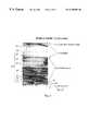
- FIG. 1is a cross section view of a layered structure illustrating one embodiment of the invention.
- FIG. 2is a cross-sectional TEM of a fabricated sample illustrating the complete layered structure of the embodiment of the invention shown in FIG. 1 .
- FIG. 3is a SIMS graph showing the Ge concentration versus depth for the fabricated sample structure shown in FIG. 2 illustrating the preferred Ge compositional layered structure of the embodiment of the invention.
- FIG. 4is an expanded SIMS view of the top part of FIG. 3 to a depth of about 1000 ⁇ showing the B and Ge concentration for the modulation-doped device region.
- FIG. 5shows the X-ray rocking curves for the ( 004 ) reflection from the relaxed fabricated layered structure shown in FIG. 2 .
- FIG. 6is a detailed cross-sectional TEM of the upper device region of the fabricated sample structure shown in FIG. 2 illustrating the composite p-channel modulation-doped device structure of the embodiment of the invention.
- FIG. 7is a detailed cross-sectional TEM of a channel region of a device structure when fabricated on a less relaxed buffer as compared to the layered structure of FIG. 1 illustrating the presence of stacking faults in the active channel.
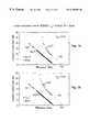
- FIG. 8is a graph of the measured hole mobility versus temperature in Kelvin (K) from Hall measurements comparing the hole mobility behavior of a high quality p-channel device structure shown in FIG. 5 with a poor quality p-channel device structure filled with stacking faults shown in FIG. 6 .
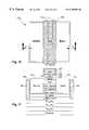
- FIG. 9is a cross section view of a layered structure illustrating a second embodiment of the invention.
- FIG. 10is a plan-view diagram of a field-effect transistor.
- FIG. 11is a cross-section view along the line 12 — 12 of FIG. 11 showing the composite p-channel layer structure.
- FIG. 12is a cross-section view of an insulating gate field-effect transistor on a composite p-channel layer structure.
- FIG. 13is an SEM micrograph of a portion of a completed, self-aligned MODFET fabricated on a composite p-channel layer structure shown in FIGS. 11 and 12.
- FIGS. 14 and 15are plots of data points of the forward current gain and maximum unilateral gain versus frequency measured with V ds equal to ⁇ 0.6V and ⁇ 1.5V, respectively, of a p-MODFET fabricated with a composite p-channel layer structure similar to the MODFET shown partially in FIG. 13 .
- a cross section view of a layered structure 10 for a composite p-channel modulation-doped SiGe heterostructureis shown to illustrate the embodiment of the invention.
- Layers 12 - 18are epitaxially grown on a single crystal semiconductor substrate 11 which may be Si, SiGe, Ge, SiC, GaAs, SOS, SOI, Bond and Etch back Silicon On Insulator (BESOI), etc. using an epitaxial growth technique such as ultra high vacuum chemical vapor depositon (UHV-CVD), molecular beam epitaxy (MBE), or rapid thermal chemical vapor deposition (RTCVD).
- UHV-CVDultra high vacuum chemical vapor depositon
- MBEmolecular beam epitaxy
- RTCVDrapid thermal chemical vapor deposition
- FIG. 2An illustration of a preferred layered structure 20 is shown in FIG. 2 which is the lower portion of layered structure 10 shown in FIG. 1 .
- FIG. 2shows a cross-sectional TEM view of a fabricated layered structure 20 comprising layers 12 A, 12 B, 12 C, and 13 - 18 grown on a preferred silicon substrate 31 .
- the corresponding Ge compositional profile of SiGe layered structure 20 of FIG. 2 as measured by secondary ion mass spectroscopy (SIMS)is shown in FIG. 3 .
- the ordinaterepresents Ge concentration in atomic percent and the abscissa represents approximate depth in microns.
- curve portions 21 ′- 27 ′, 12 B′ and 12 C′correspond to the Ge concentration in layers 21 - 27 , 12 B and 12 C shown in FIG. 2 .
- FIG. 4is an expanded view of just the top part of FIG. 3 showing the device region only.
- the ordinate on the right siderepresents Ge concentration in atomic percent and the abscissa represents approximate depth in angstroms.
- Curve 37shows the Ge concentration as a function of approximate depth.
- the ordinate on the left siderepresents boron concentration in atoms/cc and curve 39 shows the boron concentration as a function of approximate depth.
- the first epitaxial layer, described as layer 12 A in FIGS. 1 and 2, of a relaxed Si 1 ⁇ x Ge x formed on the upper surface of substrate 11 , 31is comprised of a step-graded Ge compositional layer structure comprising layers 21 - 27 .
- Layers 21 - 27have a preferred profile shown in FIG. 3 where the strain has been relieved in the buffer layers 21 - 27 or below in substrate 11 , 31 via a modified Frank Read source as a mechanism to generate new dislocations 33 which is shown in FIG. 2 and described in U.S. Pat. No. 5,659,187 which issued on Aug. 19, 1997 to F. K. Legoues and B. S. Meyerson, and herein incorporated by reference.
- Buffer layer 12comprises layers 12 A, 12 B and 12 C and may be initially undoped, relaxed, and have a Ge composition at interface 19 between layers 12 and 13 in the range from about 30% to about 50% with a preferred value of about 35%.
- the overshoot layer 12 Bfunctions to ensure a high degree of relaxation, i.e. >90% for the top Si 1 ⁇ x Ge x surface layer 12 C at interface 19 .
- layer 12 Cwould have a lattice constant which is greater than 4.956 ⁇ .
- layer 12serves to relax the strain caused by the lattice mismatch between the top surface or interface 19 of relaxed layer 12 C and the underlying Si substrate 11 , 31 where there is a 4.2% lattice misfit as Ge has a lattice spacing of 1.04 times larger than the lattice spacing of single crystal Si.
- XRDx-ray diffraction
- Curve portion 63 of curve 62shows the measured diffraction spectra for the composite hole channel 16 and 17 .
- Curve portion 64 of curve 62shows the measured diffraction spectra for the step graded layer 12 .
- Curve portion 65 of curve 62shows the measured diffraction spectra for the overshoot layer 12 B.
- Curve portion 66 of curve 62shows the measured diffraction spectra for substrate 11 .
- the preferred method of growing silicon and silicon containing filmsi.e. Si:B, Si:P, SiGe, SiGe:B, SiGe:P, SiGeC, SiGeC:B, SiGeC:P is the UHV-CVD process as described in U.S. Pat. No. 5,298,452 by B. S. Meyerson mentioned above.
- a UHV-CVD reactor suitable for growing the above-mentioned silicon and silicon containing filmsis available from Leybold-Heraeus Co. in Germany, Epigress in Sweden, and CVD Equipment Corp. in Ronkonkoma, N.Y., U.S.A.
- a p-doped relaxed SiGe layer 13 as shown in FIG. 1is first formed over layer 12 C to function as the donor or supply layer beneath an active channel.
- Layer 13may have a thickness in the range from 1 to 20 nm with a preferred thickness in the range from 4 to 5 nm and should have an electrically active donor dose in the range from 1 to 3 ⁇ 10 12 cm ⁇ 2 .
- the p-type dopant of layer 13may be incorporated in SiGe layer 13 by doping with different flows of B 2 H 6 during epitaxial growth of layer 13 .
- An example of a preferred boron dopant profile for SiGe layer 13is shown in FIG.
- An undoped strained Si layer 14is epitaxially formed above p-doped layer 13 as a spacer layer. Layer 14 functions to separate the dopants in layer 13 from the active channel layers 16 and 17 to be formed above.
- the thickness of layer 14should remain below the critical thickness of a silicon layer with respect to the lattice spacing at interface 19 of relaxed layer 12 .
- the preferred thickness of layer 13is in the range from 1 to 2 nm in the case when layer 12 at interface 19 is a relaxed Si 0.65 Ge 0.35 layer.
- a thin relaxed undoped SiGe layer 15is epitaxially grown over layer 14 and similar to layer 14 , functions as a spacer layer to further separate the dopants in layer 13 from the above composite channel 33 comprising layers 16 and 17 in order to maintain a high hole mobility in layers 16 and 17 .
- the thickness of layer 15may range from 0 to 10 nm, with the preferred thickness in the range from 4 to 5 nm.
- a compressively-strained Ge layer 16is epitaxially grown above layer 15 which functions as the first part of a composite p-channel 33 for p-channel field effect transistors.
- the epitaxial GeIn order for layer 16 to be an effective component in the composite p-channel 33 , the epitaxial Ge must be of device quality layer void of structural defects, e.g. stacking faults and any interface roughness problems between layers 16 and 17 .
- the thickness of Ge layer 16may be in the range from 0 to 25 Angstroms with a preferred thickness of 20 Angstroms as shown in FIG. 6 .
- layer 12 at interface 19must be equal to or at least equivalent in lattice spacing to a 90% relaxed Si 0.65 Ge 0.35 buffer. Otherwise, stacking faults will occur in Ge layer 16 in the case when grown on a smaller lattice spacing corresponding to a less relaxed or lower Ge content buffer layer 12 at interface 19 as shown in FIG. 7 .
- FIG. 6shows Ge layer 16 with stacking faults in the range from 10 4 to 10 6 defects/cm 2 .
- the stacking faults originating in Ge layer 16may extend upwards into Si 12 : 15 PM 1 ⁇ w Ge w layer 17 .
- Si 1 ⁇ w Ge w layer 17also should have stacking faults in the range from 10 4 to 10 6 defects/cm 2 .
- the smoothness of ti, upper surface of layer 17 at interface 42is shown.
- Stacking faultsare reduced to below 10 6 defects/cm 2 by the 90% relaxation of layer 12 at interface 19 .
- the percent of relaxation of a layercan be determined by measuring the lattice constant such as by X-ray diffraction (XRD) as mentioned above.
- XRDX-ray diffraction
- FIG. 7shows layers 12 - 18 similar to FIG. 6, but in FIG. 7 layer 12 and specifically at interface 19 the lattice constant corresponded to a relaxation of less than 90% resulting in stacking faults of above 10 6 defects/cm 2 and typically in the range from 10 6 to 10 8 defects/cm 2 which are undesireable for electronic devices.
- a compressively strained SiGe layer 17is epitaxially grown which will serve as the second part of composite channel 33 of a p-channel field effect transistor.
- the Ge composition for SiGe layer 17may range from 50% to ⁇ 100%, and the preferred composition is 80% with a thickness ranging from 40 to 100 Angstroms.
- SiGe layer 17may have the germanium content graded within SiGe layer 17 , decreasing from, for example, 0.95 Ge at the lower portion of the layer nearer the Ge layer 16 to about 0.50 Ge at the upper part of SiGe layer 17 .
- a SiGe cap layer 18is grown having the preferred Ge composition the same as that of layer 12 C at interface 19 and functions to separate p-channel 33 from the surface and to confine the hole carriers in layers 16 and 17 .
- the thickness for layer 17may range from 2 to 20 nm, with the preferred thickness in the range from 10 to 15 nm.
- Layers 13 , 15 , and 18may have the same composition of silicon and germanium to provide the same lattice spacing where the Ge content may be in the range from 20 to 50% with a preferred value of 35% in the case when layer 12 C at interface 19 has a lattice spacing equalivalent to a relaxed Si 0.65 Ge 0.35 buffer layer.
- the channel confinement of holes and its enhanced transport mobilityis a result of the higher compressive strain in the composite channel structure having two high Ge content layers with respect to the relaxed buffer layer of layer 12 at interface 19 arising from the 4.2% larger lattice constant for pure Ge relative to Si.
- the structural ability to create and enhance the compressive strain in the SiGe or Ge channel layers formed on the relaxed SiGe buffer of layer 12can significantly alter the conduction and valence bands of the p-channel layers of 16 and 17 .
- ⁇ E ⁇valence-band offset
- x′is the Ge content of the relaxed SiGe epilayer of layer 12 and x is the Ge content in the hole channel.
- This formulationis reported in a publication by R. People and J. C. Bean entitled “Band alignments of coherently strained Ge x Si 1 ⁇ x /Si heterostructures on ⁇ 001> Ge y Si 1 ⁇ y substrates”, Appl. Phys. Lett. 48 (8), Feb. 24, 1986, pp538-540 which is incorporated herein by reference.
- the valence band discontinuity ( ⁇ E ⁇ ) for layer 17 when it is a Si 0.2 Ge 0.8 channel formed over a relaxed Si 0.65 Ge 0.35 of layer 12would be 443 meV, and in the case of a pure Ge channel of layer 16 an even larger band offset of 554 meV is generated in the hole or valance band which would essentially produce a deeper quantum well or a more effective barrier for hole confinement.
- the compressive strain in the SiGe or Ge layeralso serves to split the valence band into the heavy hole and light-hole bands whereby the hole transport in the upper valence band with the lighter hole mass for carrier transport along the strained channel will result in enhanced hole mobilites that could be significantly higher as described below than in Si p-channel field effect transistors which typically has a mobility of about 75 cm 2 /Vs as reported in a publication by M. Rodder et at. entitled “A 1.2V, 0.1 ⁇ m Gate Length CMOS Technology: Design and Process Issues”, IEDM 98-623.
- the measured hole mobilities in the occupied hole band for the composite channel structureare in the range from 900 to 1400 cm 2 /Vs at 300K and in the range from 5000 to 10000 cm 2 /Vs at 20K for the case when layer 17 is a Si 0.2 Ge 0.8 channel with a thickness in the range from 7 to 8 nm and layer 16 is a Ge channel with a thickness in the range from 1.5 to 2.0 nm.
- curve 71shows the measured two-dimensional hole gases (2DHG) hole mobility behavior as a function of temperature for composite p-channel 33 of Si 1.2 Ge 0.8 /Ge when grown on a properly relaxed Si 0.65 Ge 0.35 buffer layer 12 , and compares it to curve 72 which shows the degraded mobility behavior associated with a poor quality or defective composite channel structure of Si 0.2 Ge 0.8 /Ge when grown on a lower content Si 0.75 Ge 0.25 buffer showing the sensitivity of the composite p-channel 33 to the proper design of layer 12 such as the composition profile, extent of relaxation, and remaining stacking faults and misfit dislocations.
- 2DHGtwo-dimensional hole gases
- the ordinaterepresents hole mobility ⁇ h in cm 2 /Vs and the abscissa represents temperature in degrees K.
- the degraded mobility behavior shown by curve 72is due to the presence of stacking faults occurring in the composite p-channel 33 of Si 0.2 Ge 0.8 /Ge, as illustrated in FIG. 7 in the case when the composite p-channel 33 is fabricated on a less relaxed or a lower Ge content epitaxial layer relative to layer 12 of Si 0.65 Ge 0.35 .
- the measured mobilities as shown by curve 71 for a Si 0.2 Ge 0.8 /Ge composite p-channel 33are a factor of 6 to 7 higher than found in Si p-channel field effect transistors.
- the measured mobilities as shown by curve 71 for composite p-channel 33had a defect density similar to that shown in FIG. 6 and is typically in the range from 10 4 to 10 6 defects/cm 2 .
- the measured mobilities as shown by curve 72 for composite p-channel 33had a defect density similar to that shown in FIG. 7 and is typically in the range from 10 6 to 10 8 defects/cm 2 .
- the mobility ⁇ h of composite p-channel 33equals 1,360 cm 2 /Vs at a sheet carrier density of 1.4 ⁇ 10 12 cm ⁇ 2 .
- the mobility ⁇ h of composite p-channel 33equals 9,800 cm 2 /Vs at a sheet carrier density of 3.17 ⁇ 10 12 cm ⁇ 2 .
- channel 43comprising layers 16 and 17 are formed above buffer layer 12 , SiGe layer 15 is formed above channel 43 , Si layer 14 is formed above layer 15 and the supply layer, p-doped Si 1 ⁇ x Ge x layer 13 is formed above Si layer 14 .
- a dielectric layer 81for example, silicon dioxide is formed over SiGe layer 13 .
- like referencesare used for functions corresponding to the apparatus of FIG. 1 .
- either one of spacer layersfor example, Si spacer layer 14 or SiGe spacer layer 15 may be structurally omitted from the the composite p-channel 33 layered structure 10 without introducing any major degradation in the hole confinement and mobility of the carriers in p-channel 33 .
- a thicker spacer of spacer layers 15 and 14is usually more desirable and important when attempting to optimize the carrier mobility transport at low temperatures (i.e. less than ⁇ 20 K) by further separation of the active carriers in p-channel 43 from ionized hole donors in the supply layer 13 . Nevertheless, for room temperature transport, there is minimal observable effect (if any at all) when only one spacer layer of either Si spacer layer 14 or SiGe spacer layer 15 is present to space composite channel 43 of modulation-doped device 80 from supply layer 13 .
- the composite p-channel layersare comprised of thin Ge layer 16 (less than the critical thickness at interface 19 about 10 to 20 ⁇ ) and a SiGe layer 17 .
- Ge layer 16is first formed on layer 12 C to form interface 19 .
- Layers 16 and 17function as the channel region 43 of a the field effect transistor.
- spacer layerscomprised of SiGe spacer layer 15 and Si spacer layer 14 are grown over channel layer 17 which functions to separate the dopants in the above supply layer 13 from the below active channel of layers 16 and 17 .
- a p-doped SiGe supply layer 13which functions as a donor layer or supply layer above active channel layers of 16 and 17 .
- the germanium composition and thickness for layers 16 , 17 , 15 , 14 , and 13may be the same or equivalent to those of like reference numbers in FIG. 1 which shows a composite channel layered structure 10 with the SiGe supply layer 13 below channel 33 .
- FIG. 10A plan view of a self-aligned p-type SiGe MODFET device is shown in FIG. 10.
- FIG. 11A cross section view along the line 12 — 12 of FIG. 10 is shown in FIG. 11.
- a self-aligned MODFET designis preferred to minimize the access resistance associated with a Schottky gated device structure, and the process usually requires patterning and evaporation of the gate metallization prior to the source/drain Ohmic metallization.
- a T-shaped gateis fabricated such that the gate overhang serves as a mask for the source and drain Ohmic contact evaporation which prevents shorting of the source and drain Ohmic contacts to the Schottky gate footprint. This basic process scheme has been reported in a publication by M. Arafa, K. Ismail, J. O.
- the deviceconsists of the layer structure described in FIG. 1, and in FIG. 11 like references are used for layers corresponding to the layers of FIG. 1 .
- This layer structure designdescribes a modulation-doped heterostructure whereby p-type doped layer 13 , which functions as the supply layer, is separated from layers 16 and 17 , which function as the conducting channel region, by undoped layers 14 and 15 , which function as the spacer layers.
- field-effect transistor 100consists of isolation region 104 created by selectively removing layers 13 , 14 , 15 , 16 , 17 and 18 such that the conducting composite-channel region remains only in active device region 105 .
- Isolation region 104should completely surround active channel region 105 as shown in FIG. 10 .
- Isolation region 104can then be passivated by depositing insulating material 106 , such as SiO x , in isolation region 104 after etching.
- the gate structurepreferably should be T-shaped, i.e. narrow at the bottom and wide at the top, and have the properties of a high Schottky barrier for holes, low resistivity, and a high temperature barrier for reaction with the substrate.
- the gate 107is patterned by electron-beam lithography using a bi-layer or tri-layer P(MMA-PMAA) resist system, and defined using lift-off of Ti/Mo/Pt/Au.
- gate 107is formed on layer 18 , and from bottom to top, consists of a Ti layer 108 , a Mo layer 109 , a Pt layer 110 and an Au layer 111 . This process enables gate footprint 112 dimensions less than 0.1 ⁇ m, and source-to-gate and drain-to-gate dimensions as small as 0.1 ⁇ m to be realized.
- Gate 107should form a narrow stripe that completely divides the active device region into two distinct regions on either side.
- Self-aligned source and drain Ohmic contacts 113 and 114can then be formed by evaporating a metal over active device region 105 , such that the overhang section 115 of gate 107 acts as a shadow mask to avoid shorting of source and drain contacts 113 and 114 to gate 107 .
- FIG. 12A cross-section view of an insulating gate field-effect transistor on a composite p-channel layer structure is shown in FIG. 12 .
- the deviceconsists of the layer structure described in FIG. 1, and in FIG. 12 like references are used for layers corresponding to the layers of FIG. 1 .
- the deviceadditionally consists of insulating layer 120 , which is formed on top of SiGe layer 18 .
- layer 120consists of SiO x , or Si x N y .
- the devicefurther consists of isolation region 121 , gate 122 , and source and drain contants 123 and 124 , which are configured in a similar manner as described in FIG. 10 .
- gate 122is formed on insulating layer 120 . After patterning of insulating sidewall regions 125 , gate 122 acts as a mask for the formation of self-aligned Ohmic source and drain contacts 123 and 124 .
- FIG. 13shows an SEM micrograph of a portion of a completed, self-aligned MODFET fabricated on a composite p-channel layer structure described in FIG. 10 and FIG. 11 .
- This particular devicehas a gate footprint of 0.12 ⁇ m, and source-to-gate spacing of 0.15 ⁇ m.
- FIGS. 14 and 15show graphs of the high-frequency characteristics of a self-aligned composite-channel p-MODFET at two different bias voltages.
- This deviceutilized the design shown in FIGS. 10 and 11, and had a gate footprint length of 0.09 ⁇ m and a gate width of 25 ⁇ m.
- the electrical resultswere obtained from microwave s-parameter data taken under optimum bias conditions at frequencies ranging from 5 to 40 GHz.
- the effect of parasitic elements arising from the microwave pad geometryhave been removed by measuring an open-circuit pad geometry, and then de-embedding the response of the actual device geometry from the total system response.
- the unity current gain cutoff frequency, f Tis obtained by extrapolating h 21 2 versus frequency at ⁇ 20 dB/decade until h 21 2 is equal to unity.
Landscapes
- Insulated Gate Type Field-Effect Transistor (AREA)
- Junction Field-Effect Transistors (AREA)
- Metal-Oxide And Bipolar Metal-Oxide Semiconductor Integrated Circuits (AREA)
- Thin Film Transistor (AREA)
Abstract
Description
Claims (41)
Priority Applications (8)
| Application Number | Priority Date | Filing Date | Title |
|---|---|---|---|
| US09/267,323US6350993B1 (en) | 1999-03-12 | 1999-03-12 | High speed composite p-channel Si/SiGe heterostructure for field effect devices |
| IL13467400AIL134674A (en) | 1999-03-12 | 2000-02-22 | HIGH SPEED COMPOSITE P-CHANNEL Si/SiGe HETEROSTRUCTURE FOR FIELD EFFECT DEVICES |
| CNB001036793ACN1184695C (en) | 1999-03-12 | 2000-03-02 | High-speed composite p channel si/siGe heterogeneous structure of field-effect devices |
| DE10011054ADE10011054A1 (en) | 1999-03-12 | 2000-03-07 | Layer structure arrangement used in the production of p-channel field effect transistors has silicon and germanium layers on a single crystalline substrate |
| JP2000065262AJP3457614B2 (en) | 1999-03-12 | 2000-03-09 | High-speed composite p-channel Si / SiGe heterostructure for field effect devices |
| TW089104446ATW498461B (en) | 1999-03-12 | 2000-08-30 | High speed composite p-channel Si/sige heterostructure for field effect devices |
| US09/989,770US6858502B2 (en) | 1999-03-12 | 2001-11-20 | High speed composite p-channel Si/SiGe heterostructure for field effect devices |
| US10/832,217US7084431B2 (en) | 1999-03-12 | 2004-04-26 | High speed composite p-channel Si/SiGe heterostructure for field effect devices |
Applications Claiming Priority (1)
| Application Number | Priority Date | Filing Date | Title |
|---|---|---|---|
| US09/267,323US6350993B1 (en) | 1999-03-12 | 1999-03-12 | High speed composite p-channel Si/SiGe heterostructure for field effect devices |
Related Child Applications (1)
| Application Number | Title | Priority Date | Filing Date |
|---|---|---|---|
| US09/989,770DivisionUS6858502B2 (en) | 1999-03-12 | 2001-11-20 | High speed composite p-channel Si/SiGe heterostructure for field effect devices |
Publications (1)
| Publication Number | Publication Date |
|---|---|
| US6350993B1true US6350993B1 (en) | 2002-02-26 |
Family
ID=23018301
Family Applications (3)
| Application Number | Title | Priority Date | Filing Date |
|---|---|---|---|
| US09/267,323Expired - Fee RelatedUS6350993B1 (en) | 1999-03-12 | 1999-03-12 | High speed composite p-channel Si/SiGe heterostructure for field effect devices |
| US09/989,770Expired - Fee RelatedUS6858502B2 (en) | 1999-03-12 | 2001-11-20 | High speed composite p-channel Si/SiGe heterostructure for field effect devices |
| US10/832,217Expired - LifetimeUS7084431B2 (en) | 1999-03-12 | 2004-04-26 | High speed composite p-channel Si/SiGe heterostructure for field effect devices |
Family Applications After (2)
| Application Number | Title | Priority Date | Filing Date |
|---|---|---|---|
| US09/989,770Expired - Fee RelatedUS6858502B2 (en) | 1999-03-12 | 2001-11-20 | High speed composite p-channel Si/SiGe heterostructure for field effect devices |
| US10/832,217Expired - LifetimeUS7084431B2 (en) | 1999-03-12 | 2004-04-26 | High speed composite p-channel Si/SiGe heterostructure for field effect devices |
Country Status (6)
| Country | Link |
|---|---|
| US (3) | US6350993B1 (en) |
| JP (1) | JP3457614B2 (en) |
| CN (1) | CN1184695C (en) |
| DE (1) | DE10011054A1 (en) |
| IL (1) | IL134674A (en) |
| TW (1) | TW498461B (en) |
Cited By (156)
| Publication number | Priority date | Publication date | Assignee | Title |
|---|---|---|---|---|
| US20020084000A1 (en)* | 1997-06-24 | 2002-07-04 | Eugene A. Fitzgerald | Controlling threading dislocation densities in Ge on Si using graded GeSi layers and planarization |
| US20020123167A1 (en)* | 2001-03-02 | 2002-09-05 | Fitzgerald Eugene A. | Relaxed silicon germanium platform for high speed CMOS electronics and high speed analog circuits |
| US20020125497A1 (en)* | 2001-03-02 | 2002-09-12 | Fitzgerald Eugene A. | Relaxed silicon germanium platform for high speed CMOS electronics and high speed analog circuits |
| US6455871B1 (en)* | 2000-12-27 | 2002-09-24 | Electronics And Telecommunications Research Institute | SiGe MODFET with a metal-oxide film and method for fabricating the same |
| US20020197803A1 (en)* | 2001-06-21 | 2002-12-26 | Amberwave Systems Corporation | Enhancement of p-type metal-oxide-semiconductor field effect transistors |
| US20030013323A1 (en)* | 2001-06-14 | 2003-01-16 | Richard Hammond | Method of selective removal of SiGe alloys |
| US20030034529A1 (en)* | 2000-12-04 | 2003-02-20 | Amberwave Systems Corporation | CMOS inverter and integrated circuits utilizing strained silicon surface channel MOSFETs |
| US6531351B2 (en)* | 1999-07-29 | 2003-03-11 | Stmicroelectronics, Inc. | Method for forming a CMOS circuit of GaAS/Ge on Si substrate |
| US20030049893A1 (en)* | 2001-06-08 | 2003-03-13 | Matthew Currie | Method for isolating semiconductor devices |
| US20030052334A1 (en)* | 2001-06-18 | 2003-03-20 | Lee Minjoo L. | Structure and method for a high-speed semiconductor device |
| US20030057439A1 (en)* | 2001-08-09 | 2003-03-27 | Fitzgerald Eugene A. | Dual layer CMOS devices |
| US20030062537A1 (en)* | 2001-10-02 | 2003-04-03 | Nobuyuki Sugii | Field-effect type semiconductor device for power amplifier |
| US20030077867A1 (en)* | 2001-03-02 | 2003-04-24 | Fitzergald Eugene A. | Relaxed silicon germanium platform for high speed CMOS electronics and high speed analog circuits |
| US6555839B2 (en) | 2000-05-26 | 2003-04-29 | Amberwave Systems Corporation | Buried channel strained silicon FET using a supply layer created through ion implantation |
| US6573126B2 (en) | 2000-08-16 | 2003-06-03 | Massachusetts Institute Of Technology | Process for producing semiconductor article using graded epitaxial growth |
| US20030113948A1 (en)* | 2000-01-20 | 2003-06-19 | Amberwave Systems Corporation | Low threading dislocation density relaxed mismatched epilayers without high temperature growth |
| US6583437B2 (en)* | 2000-03-17 | 2003-06-24 | Kabushiki Kaisha Toshiba | Semiconductor device and method of manufacturing the same |
| US6583015B2 (en)* | 2000-08-07 | 2003-06-24 | Amberwave Systems Corporation | Gate technology for strained surface channel and strained buried channel MOSFET devices |
| US6593641B1 (en)* | 2001-03-02 | 2003-07-15 | Amberwave Systems Corporation | Relaxed silicon germanium platform for high speed CMOS electronics and high speed analog circuits |
| US6597016B1 (en)* | 1999-01-14 | 2003-07-22 | Matsushita Electric Industrial Co., Ltd. | Semiconductor device and method for fabricating the same |
| US6602613B1 (en) | 2000-01-20 | 2003-08-05 | Amberwave Systems Corporation | Heterointegration of materials using deposition and bonding |
| US20030155592A1 (en)* | 2001-12-28 | 2003-08-21 | Masashi Shima | Semiconductor device and complementary semiconductor device |
| US6646322B2 (en)* | 2001-03-02 | 2003-11-11 | Amberwave Systems Corporation | Relaxed silicon germanium platform for high speed CMOS electronics and high speed analog circuits |
| US6649492B2 (en)* | 2002-02-11 | 2003-11-18 | International Business Machines Corporation | Strained Si based layer made by UHV-CVD, and devices therein |
| US6649480B2 (en) | 2000-12-04 | 2003-11-18 | Amberwave Systems Corporation | Method of fabricating CMOS inverter and integrated circuits utilizing strained silicon surface channel MOSFETs |
| US20030215990A1 (en)* | 2002-03-14 | 2003-11-20 | Eugene Fitzgerald | Methods for fabricating strained layers on semiconductor substrates |
| US20030219937A1 (en)* | 2002-05-15 | 2003-11-27 | Peterson Jeffrey J. | Method for co-fabricating strained and relaxed crystalline and poly-crystalline structures |
| US20030227029A1 (en)* | 2002-06-07 | 2003-12-11 | Amberwave Systems Corporation | Elevated source and drain elements for strained-channel heterojuntion field-effect transistors |
| US20030227057A1 (en)* | 2002-06-07 | 2003-12-11 | Lochtefeld Anthony J. | Strained-semiconductor-on-insulator device structures |
| US20040000268A1 (en)* | 1998-04-10 | 2004-01-01 | Massachusetts Institute Of Technology | Etch stop layer system |
| US20040005740A1 (en)* | 2002-06-07 | 2004-01-08 | Amberwave Systems Corporation | Strained-semiconductor-on-insulator device structures |
| US6680496B1 (en)* | 2002-07-08 | 2004-01-20 | Amberwave Systems Corp. | Back-biasing to populate strained layer quantum wells |
| US20040029355A1 (en)* | 2002-01-09 | 2004-02-12 | Matsushita Electric Industrial Co., Ltd. | Semiconductor device and method for fabricating the same |
| US20040026765A1 (en)* | 2002-06-07 | 2004-02-12 | Amberwave Systems Corporation | Semiconductor devices having strained dual channel layers |
| US20040031979A1 (en)* | 2002-06-07 | 2004-02-19 | Amberwave Systems Corporation | Strained-semiconductor-on-insulator device structures |
| US20040040493A1 (en)* | 2002-08-30 | 2004-03-04 | Amberwave Systems Corporation | Reduction of dislocation pile-up formation during relaxed lattice-mismatched epitaxy |
| US6703688B1 (en) | 2001-03-02 | 2004-03-09 | Amberwave Systems Corporation | Relaxed silicon germanium platform for high speed CMOS electronics and high speed analog circuits |
| US20040053470A1 (en)* | 2002-06-25 | 2004-03-18 | Lee Minjoo L. | Method for improving hole mobility enhancement in strained silicon p-type MOSFETS |
| US6724019B2 (en)* | 2000-05-25 | 2004-04-20 | Renesas Technology Corporation | Multi-layered, single crystal field effect transistor |
| US6723541B2 (en)* | 2001-07-12 | 2004-04-20 | Hitachi, Ltd. | Method of producing semiconductor device and semiconductor substrate |
| US20040075105A1 (en)* | 2002-08-23 | 2004-04-22 | Amberwave Systems Corporation | Semiconductor heterostructures having reduced dislocation pile-ups and related methods |
| US6730551B2 (en) | 2001-08-06 | 2004-05-04 | Massachusetts Institute Of Technology | Formation of planar strained layers |
| US6750130B1 (en) | 2000-01-20 | 2004-06-15 | Amberwave Systems Corporation | Heterointegration of materials using deposition and bonding |
| US20040157409A1 (en)* | 2002-07-09 | 2004-08-12 | Bruno Ghyselen | Transfer of a thin layer from a wafer comprising a buffer layer |
| US6787793B2 (en)* | 2001-12-11 | 2004-09-07 | Sharp Kabushiki Kaisha | Strained Si device with first SiGe layer with higher Ge concentration being relaxed to have substantially same lattice constant as second SiGe layer with lower Ge concentration |
| US20040173812A1 (en)* | 2003-03-07 | 2004-09-09 | Amberwave Systems Corporation | Shallow trench isolation process |
| US20040178413A1 (en)* | 2001-02-22 | 2004-09-16 | Matsushita Electric Industrial Co., Ltd. | Semiconductor device and method for producing the same |
| US20040208445A1 (en)* | 1999-03-03 | 2004-10-21 | Rj Mears Llc | Optical filter device with aperiodically arranged grating elements |
| US6830964B1 (en) | 2003-06-26 | 2004-12-14 | Rj Mears, Llc | Method for making semiconductor device including band-engineered superlattice |
| US6831292B2 (en) | 2001-09-21 | 2004-12-14 | Amberwave Systems Corporation | Semiconductor structures employing strained material layers with defined impurity gradients and methods for fabricating same |
| US6833294B1 (en) | 2003-06-26 | 2004-12-21 | Rj Mears, Llc | Method for making semiconductor device including band-engineered superlattice |
| US20040256647A1 (en)* | 2003-06-23 | 2004-12-23 | Sharp Laboratories Of America Inc. | Strained silicon finFET device |
| US20040266116A1 (en)* | 2003-06-26 | 2004-12-30 | Rj Mears, Llc | Methods of fabricating semiconductor structures having improved conductivity effective mass |
| US20050029510A1 (en)* | 2003-06-26 | 2005-02-10 | Rj Mears, Llc | Method for making electronic device comprising active optical devices with an energy band engineered superlattice |
| US20050042849A1 (en)* | 2002-06-25 | 2005-02-24 | Amberwave Systems Corporation | Reacted conductive gate electrodes |
| US20050050971A1 (en)* | 2003-01-06 | 2005-03-10 | Horning Robert D. | Methods and structure for improving wafer bow control |
| US6900103B2 (en) | 2001-03-02 | 2005-05-31 | Amberwave Systems Corporation | Relaxed silicon germanium platform for high speed CMOS electronics and high speed analog circuits |
| US20050127400A1 (en)* | 2003-12-05 | 2005-06-16 | Yee-Chia Yeo | Heterostructure resistor and method of forming the same |
| US20050136584A1 (en)* | 2003-12-23 | 2005-06-23 | Boyan Boyanov | Strained transistor integration for CMOS |
| US20050136624A1 (en)* | 2001-04-04 | 2005-06-23 | Massachusetts Institute Of Technology | Method for semiconductor device fabrication |
| US20050153495A1 (en)* | 2004-01-12 | 2005-07-14 | Chartered Semiconductor Manufacturing Ltd. | Silicon - germanium virtual substrate and method of fabricating the same |
| US20050156255A1 (en)* | 2004-01-21 | 2005-07-21 | Taiwan Semiconductor Manufacturing Co. | Noble high-k device |
| US20050167653A1 (en)* | 2003-06-26 | 2005-08-04 | Rj Mears, Llc | Semiconductor device including a superlattice with regions defining a semiconductor junction |
| US20050170590A1 (en)* | 2003-06-26 | 2005-08-04 | Rj Mears, Llc. | Method for making a semiconductor device including a superlattice with regions defining a semiconductor junction |
| US20050170591A1 (en)* | 2003-06-26 | 2005-08-04 | Rj Mears, Llc | Method for making a semiconductor device including a superlattice and adjacent semiconductor layer with doped regions defining a semiconductor junction |
| US20050167649A1 (en)* | 2003-06-26 | 2005-08-04 | Rj Mears, Llc | Semiconductor device including a superlattice and adjacent semiconductor layer with doped regions defining a semiconductor junction |
| US20050176204A1 (en)* | 2002-06-10 | 2005-08-11 | Amberwave Systems Corporation | Source and drain elements |
| US6933518B2 (en) | 2001-09-24 | 2005-08-23 | Amberwave Systems Corporation | RF circuits including transistors having strained material layers |
| US20050195012A1 (en)* | 2004-03-02 | 2005-09-08 | Atsushi Sueoka | Semiconductor device |
| US20050208780A1 (en)* | 2003-05-30 | 2005-09-22 | International Business Machines Corporation | High-quality SGOI by oxidation near the alloy melting temperature |
| US20050274981A1 (en)* | 2003-07-30 | 2005-12-15 | Ho Lee | Multi-layered structure including an epitaxial layer having a low dislocation defect density, semiconductor device comprising the same, and method of fabricating the semiconductor device |
| US20050279991A1 (en)* | 2003-06-26 | 2005-12-22 | Rj Mears, Llc | Semiconductor device including a superlattice having at least one group of substantially undoped layers |
| US20050282330A1 (en)* | 2003-06-26 | 2005-12-22 | Rj Mears, Llc | Method for making a semiconductor device including a superlattice having at least one group of substantially undoped layers |
| US20050285097A1 (en)* | 2004-06-24 | 2005-12-29 | Huiling Shang | Integration of strained Ge into advanced CMOS technology |
| US20060001126A1 (en)* | 2004-06-30 | 2006-01-05 | Chandra Mouli | Transistor structures and transistors with a germanium-containing channel |
| US20060014366A1 (en)* | 2002-06-07 | 2006-01-19 | Amberwave Systems Corporation | Control of strain in device layers by prevention of relaxation |
| US20060011905A1 (en)* | 2003-06-26 | 2006-01-19 | Rj Mears, Llc | Semiconductor device comprising a superlattice dielectric interface layer |
| US20060011984A1 (en)* | 2002-06-07 | 2006-01-19 | Amberwave Systems Corporation | Control of strain in device layers by selective relaxation |
| US20060019454A1 (en)* | 2003-06-26 | 2006-01-26 | Rj Mears, Llc | Method for making a semiconductor device comprising a superlattice dielectric interface layer |
| US20060040503A1 (en)* | 2004-08-17 | 2006-02-23 | Sun-Jay Chang | Process for fabricating a strained channel MOSFET device |
| US20060048700A1 (en)* | 2002-09-05 | 2006-03-09 | Wanlass Mark W | Method for achieving device-quality, lattice-mismatched, heteroepitaxial active layers |
| US20060113605A1 (en)* | 2004-12-01 | 2006-06-01 | Amberwave Systems Corporation | Hybrid fin field-effect transistor structures and related methods |
| US20060113603A1 (en)* | 2004-12-01 | 2006-06-01 | Amberwave Systems Corporation | Hybrid semiconductor-on-insulator structures and related methods |
| US20060118863A1 (en)* | 2004-10-07 | 2006-06-08 | Gary Dolny | Bandgap engineered MOS-gated power transistors |
| US20060128096A1 (en)* | 2003-02-10 | 2006-06-15 | Arup Bhattacharyya | Methods of forming semiconductor devices |
| US20060141796A1 (en)* | 2004-12-28 | 2006-06-29 | Hynix Semiconductor, Inc. | Method of manufacturing semiconductor device |
| US20060151787A1 (en)* | 2005-01-12 | 2006-07-13 | International Business Machines Corporation | LOW CONCENTRATION SiGe BUFFER DURING STRAINED Si GROWTH OF SSGOI MATERIAL FOR DOPANT DIFFUSION CONTROL AND DEFECT REDUCTION |
| US20060202189A1 (en)* | 2003-06-26 | 2006-09-14 | Rj Mears, Llc | Semiconductor device including a memory cell with a negative differential resistance (ndr) device |
| US20060220118A1 (en)* | 2003-06-26 | 2006-10-05 | Rj Mears, Llc | Semiconductor device including a dopant blocking superlattice |
| US20060226502A1 (en)* | 2003-06-26 | 2006-10-12 | Rj Mears, Llc | Microelectromechanical Systems (MEMS) Device Including a Superlattice |
| US7123792B1 (en) | 1999-03-05 | 2006-10-17 | Rj Mears, Llc | Configurable aperiodic grating device |
| US20060231857A1 (en)* | 2003-06-26 | 2006-10-19 | Rj Mears, Llc | Method for making a semiconductor device including a memory cell with a negative differential resistance (ndr) device |
| US20060243964A1 (en)* | 2003-06-26 | 2006-11-02 | Rj Mears, Llc | Method for making a semiconductor device having a semiconductor-on-insulator configuration and a superlattice |
| US7138649B2 (en) | 2001-08-09 | 2006-11-21 | Amberwave Systems Corporation | Dual-channel CMOS transistors with differentially strained channels |
| US20060261327A1 (en)* | 2003-06-26 | 2006-11-23 | Rj Mears, Llc | Semiconductor device having a semiconductor-on-insulator configuration and a superlattice |
| US20060267130A1 (en)* | 2003-06-26 | 2006-11-30 | Rj Mears, Llc | Semiconductor Device Including Shallow Trench Isolation (STI) Regions with a Superlattice Therebetween |
| US20060270169A1 (en)* | 2003-06-26 | 2006-11-30 | Rj Mears, Llc | Method for Making a Semiconductor Device Including Shallow Trench Isolation (STI) Regions with a Superlattice Therebetween |
| US20060273299A1 (en)* | 2003-06-26 | 2006-12-07 | Rj Mears, Llc | Method for making a semiconductor device including a dopant blocking superlattice |
| US7153763B2 (en) | 2003-06-26 | 2006-12-26 | Rj Mears, Llc | Method for making a semiconductor device including band-engineered superlattice using intermediate annealing |
| US20060292889A1 (en)* | 2003-06-26 | 2006-12-28 | Rj Mears, Llc | FINFET Including a Superlattice |
| US20060289916A1 (en)* | 2004-10-07 | 2006-12-28 | Chanho Park | Power Trench MOSFETs Having SiGe/Si Channel Structure |
| US20060292818A1 (en)* | 2003-06-26 | 2006-12-28 | Rj Mears, Llc | Method for Making a Semiconductor Device Having a Semiconductor-on-Insulator (SOI) Configuration and Including a Superlattice on a Thin Semiconductor Layer |
| US20060289049A1 (en)* | 2003-06-26 | 2006-12-28 | Rj Mears, Llc | Semiconductor Device Having a Semiconductor-on-Insulator (SOI) Configuration and Including a Superlattice on a Thin Semiconductor Layer |
| US20060292765A1 (en)* | 2003-06-26 | 2006-12-28 | Rj Mears, Llc | Method for Making a FINFET Including a Superlattice |
| US20070007508A1 (en)* | 2003-06-26 | 2007-01-11 | Rj Mears, Llc | Semiconductor Device Including a Strained Superlattice Layer Above a Stress Layer |
| US20070010040A1 (en)* | 2003-06-26 | 2007-01-11 | Rj Mears, Llc | Method for Making a Semiconductor Device Including a Strained Superlattice Layer Above a Stress Layer |
| US20070012909A1 (en)* | 2003-06-26 | 2007-01-18 | Rj Mears, Llc | Semiconductor Device Including a Strained Superlattice Between at Least One Pair of Spaced Apart Stress Regions |
| US20070013002A1 (en)* | 2003-12-23 | 2007-01-18 | Klaus Schruefer | Field effect transistor with a heterostructure and associated production method |
| US20070012912A1 (en)* | 2003-06-26 | 2007-01-18 | Rj Mears, Llc | Semiconductor Device Including a Strained Superlattice and Overlying Stress Layer and Related Methods |
| US20070015344A1 (en)* | 2003-06-26 | 2007-01-18 | Rj Mears, Llc | Method for Making a Semiconductor Device Including a Strained Superlattice Between at Least One Pair of Spaced Apart Stress Regions |
| US20070012999A1 (en)* | 2003-06-26 | 2007-01-18 | Rj Mears, Llc | Method for Making a Semiconductor Device Including Regions of Band-Engineered Semiconductor Superlattice to Reduce Device-On Resistance |
| US20070012911A1 (en)* | 2003-06-26 | 2007-01-18 | Rj Mears, Llc | Semiconductor Device Including Regions of Band-Engineered Semiconductor Superlattice to Reduce Device-On Resistance |
| US20070020860A1 (en)* | 2003-06-26 | 2007-01-25 | Rj Mears, Llc | Method for Making Semiconductor Device Including a Strained Superlattice and Overlying Stress Layer and Related Methods |
| US20070020833A1 (en)* | 2003-06-26 | 2007-01-25 | Rj Mears, Llc | Method for Making a Semiconductor Device Including a Channel with a Non-Semiconductor Layer Monolayer |
| US20070063185A1 (en)* | 2003-06-26 | 2007-03-22 | Rj Mears, Llc | Semiconductor device including a front side strained superlattice layer and a back side stress layer |
| US20070063186A1 (en)* | 2003-06-26 | 2007-03-22 | Rj Mears, Llc | Method for making a semiconductor device including a front side strained superlattice layer and a back side stress layer |
| US20070158640A1 (en)* | 2005-12-22 | 2007-07-12 | Rj Mears, Llc | Electronic device including a poled superlattice having a net electrical dipole moment |
| US20070161138A1 (en)* | 2005-12-22 | 2007-07-12 | Rj Mears, Llc | Method for making an electronic device including a poled superlattice having a net electrical dipole moment |
| US20070197006A1 (en)* | 2006-02-21 | 2007-08-23 | Rj Mears, Llc | Method for making a semiconductor device comprising a lattice matching layer |
| US20070264801A1 (en)* | 2006-05-09 | 2007-11-15 | Cody Nyles W | Semiconductor buffer structures |
| US20080017952A1 (en)* | 2006-07-24 | 2008-01-24 | Asm America, Inc. | Strained layers within semiconductor buffer structures |
| US7332417B2 (en) | 2003-01-27 | 2008-02-19 | Amberwave Systems Corporation | Semiconductor structures with structural homogeneity |
| US20080179588A1 (en)* | 2007-01-25 | 2008-07-31 | Mears Technologies, Inc. | Semiconductor device including a metal-to-semiconductor superlattice interface layer and related methods |
| US20080191248A1 (en)* | 2007-02-09 | 2008-08-14 | Qi Wang | Scalable Power Field Effect Transistor with Improved Heavy Body Structure and Method of Manufacture |
| US20080197340A1 (en)* | 2007-02-16 | 2008-08-21 | Rj Mears, Llc | Multiple-wavelength opto-electronic device including a superlattice |
| US20080197341A1 (en)* | 2007-02-16 | 2008-08-21 | Rj Mears, Llc | Method for making a multiple-wavelength opto-electronic device including a superlattice |
| US7435690B2 (en)* | 2004-03-25 | 2008-10-14 | Commissariat A L'energie Atomique | Method of preparing a silicon dioxide layer by high temperature oxidation on a substrate having, at least on the surface, germanium or a silicon-germanium alloy |
| US20080258134A1 (en)* | 2007-04-23 | 2008-10-23 | Mears Technologies, Inc. | Method for making a semiconductor device including shallow trench isolation (sti) regions with maskless superlattice deposition following sti formation and related structures |
| US20090075445A1 (en)* | 2005-03-11 | 2009-03-19 | Jack Kavalieros | Complementary metal oxide semiconductor integrated circuit using uniaxial compressive stress and biaxial compressive stress |
| US20090081839A1 (en)* | 1999-03-12 | 2009-03-26 | International Business Machines Corporation | High speed ge channel heterostructures for field effect devices |
| US20090146184A1 (en)* | 2007-12-05 | 2009-06-11 | Electronics And Telecommunications Research Institute | Semiconductor device with t-gate electrode and method for fabricating the same |
| US20090194811A1 (en)* | 2007-12-13 | 2009-08-06 | James Pan | Structure and Method for Forming Field Effect Transistor with Low Resistance Channel Region |
| US7659539B2 (en) | 2003-06-26 | 2010-02-09 | Mears Technologies, Inc. | Semiconductor device including a floating gate memory cell with a superlattice channel |
| US7781827B2 (en) | 2007-01-24 | 2010-08-24 | Mears Technologies, Inc. | Semiconductor device with a vertical MOSFET including a superlattice and related methods |
| US20100219396A1 (en)* | 2007-03-29 | 2010-09-02 | Been-Yih Jin | Mechanism for Forming a Remote Delta Doping Layer of a Quantum Well Structure |
| US20100254425A1 (en)* | 2007-06-29 | 2010-10-07 | International Business Machines Corporation | Phase change material based temperature sensor |
| US20110121266A1 (en)* | 2008-12-31 | 2011-05-26 | Prashant Majhi | Quantum well mosfet channels having uni-axial strain caused by metal source/drains, and conformal regrowth source/drains |
| US20120119205A1 (en)* | 2009-12-28 | 2012-05-17 | Sony Corporation | Thin film transistor, display device, and electronic device |
| US8455858B2 (en) | 2010-04-16 | 2013-06-04 | Tsinghua University | Semiconductor structure for reducing band-to-band tunneling (BTBT) leakage |
| US20130295757A1 (en)* | 2012-05-04 | 2013-11-07 | BAE Systems Information and Electronic Systems Integration Inc. | Short gate-length high electron-mobility transistors with asymmetric recess and self-aligned ohmic electrodes |
| US20140167161A1 (en)* | 2012-12-13 | 2014-06-19 | Globalfoundries Singapore Pte. Ltd. | Floating body cell |
| US20150076558A1 (en)* | 2013-09-13 | 2015-03-19 | Taiwan Semiconductor Manufacturing Company Ltd. | Semiconductor structure and the manufacturing method thereof |
| US9127345B2 (en) | 2012-03-06 | 2015-09-08 | Asm America, Inc. | Methods for depositing an epitaxial silicon germanium layer having a germanium to silicon ratio greater than 1:1 using silylgermane and a diluent |
| US9218963B2 (en) | 2013-12-19 | 2015-12-22 | Asm Ip Holding B.V. | Cyclical deposition of germanium |
| US9275996B2 (en) | 2013-11-22 | 2016-03-01 | Mears Technologies, Inc. | Vertical semiconductor devices including superlattice punch through stop layer and related methods |
| US9406753B2 (en) | 2013-11-22 | 2016-08-02 | Atomera Incorporated | Semiconductor devices including superlattice depletion layer stack and related methods |
| US9472575B2 (en)* | 2015-02-06 | 2016-10-18 | International Business Machines Corporation | Formation of strained fins in a finFET device |
| US9558939B1 (en) | 2016-01-15 | 2017-01-31 | Atomera Incorporated | Methods for making a semiconductor device including atomic layer structures using N2O as an oxygen source |
| US9716147B2 (en) | 2014-06-09 | 2017-07-25 | Atomera Incorporated | Semiconductor devices with enhanced deterministic doping and related methods |
| US9722046B2 (en) | 2014-11-25 | 2017-08-01 | Atomera Incorporated | Semiconductor device including a superlattice and replacement metal gate structure and related methods |
| US9721790B2 (en) | 2015-06-02 | 2017-08-01 | Atomera Incorporated | Method for making enhanced semiconductor structures in single wafer processing chamber with desired uniformity control |
| US9899479B2 (en) | 2015-05-15 | 2018-02-20 | Atomera Incorporated | Semiconductor devices with superlattice layers providing halo implant peak confinement and related methods |
| US10109748B2 (en) | 2009-04-01 | 2018-10-23 | Taiwan Semiconductor Manufacturing Company, Ltd. | High-mobility multiple-gate transistor with improved on-to-off current ratio |
| US10269970B2 (en) | 2009-05-29 | 2019-04-23 | Taiwan Semiconductor Manufacturing Company, Ltd. | Gradient ternary or quaternary multiple-gate transistor |
| US10553423B2 (en) | 2012-09-05 | 2020-02-04 | Asm Ip Holding B.V. | Atomic layer deposition of GeO2 |
| US20230197842A1 (en)* | 2021-12-20 | 2023-06-22 | International Business Machines Corporation | High electron mobility transistor with gate electrode below the channel |
Families Citing this family (60)
| Publication number | Priority date | Publication date | Assignee | Title |
|---|---|---|---|---|
| DE10025833A1 (en)* | 2000-05-25 | 2001-11-29 | Rubitec Gesellschaft Fuer Innovation & Technologie Ruhr Univ Bochum Mbh | Semiconductor layer system and method for producing a semiconductor layer system with increased resistance to thermal processing |
| US6844227B2 (en) | 2000-12-26 | 2005-01-18 | Matsushita Electric Industrial Co., Ltd. | Semiconductor devices and method for manufacturing the same |
| US6593625B2 (en)* | 2001-06-12 | 2003-07-15 | International Business Machines Corporation | Relaxed SiGe layers on Si or silicon-on-insulator substrates by ion implantation and thermal annealing |
| KR100776965B1 (en)* | 2001-08-06 | 2007-11-21 | 가부시키가이샤 섬코 | Semiconductor Substrate and Field Effect Transistor and Manufacturing Method Thereof |
| WO2003015140A1 (en)* | 2001-08-06 | 2003-02-20 | Sumitomo Mitsubishi Silicon Corporation | Semiconductor substrate, field-effct transistor, and their manufacturing methods |
| KR100460201B1 (en)* | 2002-04-08 | 2004-12-08 | 한국전자통신연구원 | Manufacturing method of a virtual substrate for SiGe/Si hetero-junction field-effect transistor |
| JP2003347229A (en)* | 2002-05-31 | 2003-12-05 | Renesas Technology Corp | Method of manufacturing semiconductor device and semiconductor device |
| KR100874788B1 (en)* | 2003-01-07 | 2008-12-18 | 에스. 오. 이. 떼끄 씰리꽁 오 냉쉴라또흐 떼끄놀로지 | Recycling method by mechanical means of a wafer including a peeling structure after thin layer peeling |
| US20090325362A1 (en)* | 2003-01-07 | 2009-12-31 | Nabil Chhaimi | Method of recycling an epitaxied donor wafer |
| EP1439570A1 (en)* | 2003-01-14 | 2004-07-21 | Interuniversitair Microelektronica Centrum ( Imec) | SiGe strain relaxed buffer for high mobility devices and a method of fabricating it |
| US7838875B1 (en) | 2003-01-22 | 2010-11-23 | Tsang Dean Z | Metal transistor device |
| US6995427B2 (en) | 2003-01-29 | 2006-02-07 | S.O.I.Tec Silicon On Insulator Technologies S.A. | Semiconductor structure for providing strained crystalline layer on insulator and method for fabricating same |
| US6911379B2 (en)* | 2003-03-05 | 2005-06-28 | Taiwan Semiconductor Manufacturing Company, Ltd. | Method of forming strained silicon on insulator substrate |
| US6949451B2 (en)* | 2003-03-10 | 2005-09-27 | Taiwan Semiconductor Manufacturing Company, Ltd. | SOI chip with recess-resistant buried insulator and method of manufacturing the same |
| US7238595B2 (en)* | 2003-03-13 | 2007-07-03 | Asm America, Inc. | Epitaxial semiconductor deposition methods and structures |
| US7682947B2 (en)* | 2003-03-13 | 2010-03-23 | Asm America, Inc. | Epitaxial semiconductor deposition methods and structures |
| US6902962B2 (en)* | 2003-04-04 | 2005-06-07 | Taiwan Semiconductor Manufacturing Company, Ltd. | Silicon-on-insulator chip with multiple crystal orientations |
| KR20060039915A (en)* | 2003-07-30 | 2006-05-09 | 에이에스엠 아메리카, 인코포레이티드 | Epitaxial Growth of a Relaxed Silicon Germanium Layer |
| US7045836B2 (en)* | 2003-07-31 | 2006-05-16 | Taiwan Semiconductor Manufacturing Company, Ltd. | Semiconductor structure having a strained region and a method of fabricating same |
| US6855963B1 (en)* | 2003-08-29 | 2005-02-15 | International Business Machines Corporation | Ultra high-speed Si/SiGe modulation-doped field effect transistors on ultra thin SOI/SGOI substrate |
| US7495267B2 (en)* | 2003-09-08 | 2009-02-24 | Taiwan Semiconductor Manufacturing Company, Ltd. | Semiconductor structure having a strained region and a method of fabricating same |
| US6831350B1 (en) | 2003-10-02 | 2004-12-14 | Freescale Semiconductor, Inc. | Semiconductor structure with different lattice constant materials and method for forming the same |
| US6919258B2 (en)* | 2003-10-02 | 2005-07-19 | Freescale Semiconductor, Inc. | Semiconductor device incorporating a defect controlled strained channel structure and method of making the same |
| US7078282B2 (en)* | 2003-12-30 | 2006-07-18 | Intel Corporation | Replacement gate flow facilitating high yield and incorporation of etch stop layers and/or stressed films |
| JP4507604B2 (en)* | 2004-01-16 | 2010-07-21 | 信越半導体株式会社 | Method for measuring strain of bonded strained wafer |
| GB2411047B (en)* | 2004-02-13 | 2008-01-02 | Iqe Silicon Compounds Ltd | Compound semiconductor device and method of producing the same |
| US20060011906A1 (en)* | 2004-07-14 | 2006-01-19 | International Business Machines Corporation | Ion implantation for suppression of defects in annealed SiGe layers |
| US7384829B2 (en)* | 2004-07-23 | 2008-06-10 | International Business Machines Corporation | Patterned strained semiconductor substrate and device |
| US8110863B2 (en) | 2005-06-01 | 2012-02-07 | Sandisk 3D Llc | TFT charge storage memory cell having high-mobility corrugated channel |
| TWI258172B (en)* | 2005-08-24 | 2006-07-11 | Ind Tech Res Inst | Transistor device with strained Ge layer by selectively grown and fabricating method thereof |
| EP1763069B1 (en)* | 2005-09-07 | 2016-04-13 | Soitec | Method for forming a semiconductor heterostructure |
| US7902046B2 (en)* | 2005-09-19 | 2011-03-08 | The Board Of Trustees Of The Leland Stanford Junior University | Thin buffer layers for SiGe growth on mismatched substrates |
| US7648853B2 (en) | 2006-07-11 | 2010-01-19 | Asm America, Inc. | Dual channel heterostructure |
| CN100447950C (en)* | 2007-01-26 | 2008-12-31 | 厦门大学 | Preparation method of silicon germanium virtual substrate with low dislocation density |
| US7569869B2 (en)* | 2007-03-29 | 2009-08-04 | Intel Corporation | Transistor having tensile strained channel and system including same |
| US7531854B2 (en) | 2007-05-04 | 2009-05-12 | Dsm Solutions, Inc. | Semiconductor device having strain-inducing substrate and fabrication methods thereof |
| US7791063B2 (en)* | 2007-08-30 | 2010-09-07 | Intel Corporation | High hole mobility p-channel Ge transistor structure on Si substrate |
| FR2921749B1 (en)* | 2007-09-27 | 2014-08-29 | Soitec Silicon On Insulator | METHOD FOR MANUFACTURING A STRUCTURE COMPRISING A SUBSTRATE AND A LAYER DEPOSITED ON ONE OF ITS FACES |
| FR2929758B1 (en)* | 2008-04-07 | 2011-02-11 | Commissariat Energie Atomique | TRANSFER METHOD USING A FERROELECTRIC SUBSTRATE |
| US8222657B2 (en)* | 2009-02-23 | 2012-07-17 | The Penn State Research Foundation | Light emitting apparatus |
| US8816391B2 (en) | 2009-04-01 | 2014-08-26 | Taiwan Semiconductor Manufacturing Company, Ltd. | Source/drain engineering of devices with high-mobility channels |
| US8455860B2 (en) | 2009-04-30 | 2013-06-04 | Taiwan Semiconductor Manufacturing Company, Ltd. | Reducing source/drain resistance of III-V based transistors |
| US8384128B2 (en) | 2009-05-15 | 2013-02-26 | Intel Corporation | Carrier mobility in surface-channel transistors, apparatus made therewith, and systems containing same |
| US8617976B2 (en) | 2009-06-01 | 2013-12-31 | Taiwan Semiconductor Manufacturing Company, Ltd. | Source/drain re-growth for manufacturing III-V based transistors |
| WO2011037574A1 (en)* | 2009-09-25 | 2011-03-31 | Hewlett-Packard Development Company, L.P. | Silicon-germanium, quantum-well, light-emitting diode |
| US8193523B2 (en) | 2009-12-30 | 2012-06-05 | Intel Corporation | Germanium-based quantum well devices |
| CN102194859B (en)* | 2010-03-05 | 2013-05-01 | 中国科学院微电子研究所 | High mobility III-V semiconductor MOS interface structure |
| US8455929B2 (en) | 2010-06-30 | 2013-06-04 | Taiwan Semiconductor Manufacturing Company, Ltd. | Formation of III-V based devices on semiconductor substrates |
| JP6017125B2 (en)* | 2011-09-16 | 2016-10-26 | ルネサスエレクトロニクス株式会社 | Semiconductor device and manufacturing method of semiconductor device |
| US8963162B2 (en) | 2011-12-28 | 2015-02-24 | Taiwan Semiconductor Manufacturing Company, Ltd. | High electron mobility transistor |
| US9214577B2 (en) | 2012-02-28 | 2015-12-15 | International Business Machines Corporation | Reduced light degradation due to low power deposition of buffer layer |
| EP2701198A3 (en)* | 2012-08-24 | 2017-06-28 | Imec | Device with strained layer for quantum well confinement and method for manufacturing thereof |
| EP2741320B1 (en)* | 2012-12-05 | 2020-06-17 | IMEC vzw | Manufacturing method of a finfet device with dual-strained channels |
| US9276077B2 (en)* | 2013-05-21 | 2016-03-01 | Globalfoundries Inc. | Contact metallurgy for self-aligned high electron mobility transistor |
| US9231094B2 (en)* | 2013-05-21 | 2016-01-05 | Globalfoundries Inc. | Elemental semiconductor material contact for high electron mobility transistor |
| KR102257423B1 (en)* | 2015-01-23 | 2021-05-31 | 삼성전자주식회사 | Semiconductor substrate and semiconductor device including the same |
| FR3076394A1 (en)* | 2018-01-04 | 2019-07-05 | Stmicroelectronics (Rousset) Sas | MOS TRANSISTOR SPACERS AND METHOD FOR MANUFACTURING SAME |
| CN111213241B (en)* | 2018-06-30 | 2023-09-22 | 魏进 | Semiconductor device, semiconductor apparatus, and method of manufacturing the same |
| US10510871B1 (en) | 2018-08-16 | 2019-12-17 | Taiwan Semiconductor Manufacturing Company, Ltd. | Semiconductor device and method |
| CN118866972B (en)* | 2024-09-24 | 2025-01-28 | 中国科学技术大学 | Heterojunction field effect transistor device structure and preparation method thereof |
Citations (27)
| Publication number | Priority date | Publication date | Assignee | Title |
|---|---|---|---|---|
| US4994866A (en) | 1988-01-07 | 1991-02-19 | Fujitsu Limited | Complementary semiconductor device |
| US5019882A (en) | 1989-05-15 | 1991-05-28 | International Business Machines Corporation | Germanium channel silicon MOSFET |
| US5036374A (en) | 1987-04-09 | 1991-07-30 | Seiko Instruments Inc. | Insulated gate semiconductor device using compound semiconductor at the channel |
| US5216271A (en) | 1990-09-28 | 1993-06-01 | Kabushiki Kaisha Toshiba | BiCMOS device with low bandgap CMOS contact regions and low bandgap bipolar base region |
| US5221413A (en) | 1991-04-24 | 1993-06-22 | At&T Bell Laboratories | Method for making low defect density semiconductor heterostructure and devices made thereby |
| US5223724A (en) | 1990-07-31 | 1993-06-29 | At & T Bell Laboratories | Multiple channel high electron mobility transistor |
| US5241197A (en) | 1989-01-25 | 1993-08-31 | Hitachi, Ltd. | Transistor provided with strained germanium layer |
| US5259918A (en) | 1991-06-12 | 1993-11-09 | International Business Machines Corporation | Heteroepitaxial growth of germanium on silicon by UHV/CVD |
| US5272365A (en) | 1990-03-29 | 1993-12-21 | Kabushiki Kaisha Toshiba | Silicon transistor device with silicon-germanium electron gas hetero structure channel |
| US5285088A (en) | 1991-09-17 | 1994-02-08 | Nec Corporation | High electron mobility transistor |
| US5298452A (en) | 1986-09-12 | 1994-03-29 | International Business Machines Corporation | Method and apparatus for low temperature, low pressure chemical vapor deposition of epitaxial silicon layers |
| US5350940A (en) | 1984-02-02 | 1994-09-27 | Fastran, Inc. | Enhanced mobility metal oxide semiconductor devices |
| US5357119A (en) | 1993-02-19 | 1994-10-18 | Board Of Regents Of The University Of California | Field effect devices having short period superlattice structures using Si and Ge |
| US5436474A (en) | 1993-05-07 | 1995-07-25 | Board Of Regents Of The University Of Texas System | Modulation doped field effect transistor having built-in drift field |
| US5442205A (en) | 1991-04-24 | 1995-08-15 | At&T Corp. | Semiconductor heterostructure devices with strained semiconductor layers |
| US5451800A (en) | 1992-12-02 | 1995-09-19 | International Business Machines Corporation | Metal oxide semiconductor heterojunction field effect transistor (MOSHFET) |
| US5461250A (en) | 1992-08-10 | 1995-10-24 | International Business Machines Corporation | SiGe thin film or SOI MOSFET and method for making the same |
| US5523592A (en)* | 1993-02-03 | 1996-06-04 | Hitachi, Ltd. | Semiconductor optical device, manufacturing method for the same, and opto-electronic integrated circuit using the same |
| US5534713A (en)* | 1994-05-20 | 1996-07-09 | International Business Machines Corporation | Complementary metal-oxide semiconductor transistor logic using strained SI/SIGE heterostructure layers |
| US5561302A (en) | 1994-09-26 | 1996-10-01 | Motorola, Inc. | Enhanced mobility MOSFET device and method |
| US5659187A (en) | 1991-05-31 | 1997-08-19 | International Business Machines Corporation | Low defect density/arbitrary lattice constant heteroepitaxial layers |
| US5665981A (en) | 1994-10-24 | 1997-09-09 | Micron Technology, Inc. | Thin film transistors and method of promoting large crystal grain size in the formation of polycrystalline silicon alloy thin films |
| US5686744A (en) | 1996-06-17 | 1997-11-11 | Northern Telecom Limited | Complementary modulation-doped field-effect transistors |
| US5698869A (en) | 1994-09-13 | 1997-12-16 | Kabushiki Kaisha Toshiba | Insulated-gate transistor having narrow-bandgap-source |
| US5726487A (en) | 1992-03-30 | 1998-03-10 | Sony Corporation | Semiconductor device having an improved thin film transistor |
| US5821577A (en) | 1991-01-10 | 1998-10-13 | International Business Machines Corporation | Graded channel field effect transistor |
| US6059895A (en)* | 1997-04-30 | 2000-05-09 | International Business Machines Corporation | Strained Si/SiGe layers on insulator |
Family Cites Families (1)
| Publication number | Priority date | Publication date | Assignee | Title |
|---|---|---|---|---|
| JPS61294877A (en) | 1985-06-24 | 1986-12-25 | Nippon Telegr & Teleph Corp <Ntt> | Semiconductor device |
- 1999
- 1999-03-12USUS09/267,323patent/US6350993B1/ennot_activeExpired - Fee Related
- 2000
- 2000-02-22ILIL13467400Apatent/IL134674A/ennot_activeIP Right Cessation
- 2000-03-02CNCNB001036793Apatent/CN1184695C/ennot_activeExpired - Fee Related
- 2000-03-07DEDE10011054Apatent/DE10011054A1/ennot_activeCeased
- 2000-03-09JPJP2000065262Apatent/JP3457614B2/ennot_activeExpired - Fee Related
- 2000-08-30TWTW089104446Apatent/TW498461B/ennot_activeIP Right Cessation
- 2001
- 2001-11-20USUS09/989,770patent/US6858502B2/ennot_activeExpired - Fee Related
- 2004
- 2004-04-26USUS10/832,217patent/US7084431B2/ennot_activeExpired - Lifetime
Patent Citations (27)
| Publication number | Priority date | Publication date | Assignee | Title |
|---|---|---|---|---|
| US5350940A (en) | 1984-02-02 | 1994-09-27 | Fastran, Inc. | Enhanced mobility metal oxide semiconductor devices |
| US5298452A (en) | 1986-09-12 | 1994-03-29 | International Business Machines Corporation | Method and apparatus for low temperature, low pressure chemical vapor deposition of epitaxial silicon layers |
| US5036374A (en) | 1987-04-09 | 1991-07-30 | Seiko Instruments Inc. | Insulated gate semiconductor device using compound semiconductor at the channel |
| US4994866A (en) | 1988-01-07 | 1991-02-19 | Fujitsu Limited | Complementary semiconductor device |
| US5241197A (en) | 1989-01-25 | 1993-08-31 | Hitachi, Ltd. | Transistor provided with strained germanium layer |
| US5019882A (en) | 1989-05-15 | 1991-05-28 | International Business Machines Corporation | Germanium channel silicon MOSFET |
| US5272365A (en) | 1990-03-29 | 1993-12-21 | Kabushiki Kaisha Toshiba | Silicon transistor device with silicon-germanium electron gas hetero structure channel |
| US5223724A (en) | 1990-07-31 | 1993-06-29 | At & T Bell Laboratories | Multiple channel high electron mobility transistor |
| US5216271A (en) | 1990-09-28 | 1993-06-01 | Kabushiki Kaisha Toshiba | BiCMOS device with low bandgap CMOS contact regions and low bandgap bipolar base region |
| US5821577A (en) | 1991-01-10 | 1998-10-13 | International Business Machines Corporation | Graded channel field effect transistor |
| US5221413A (en) | 1991-04-24 | 1993-06-22 | At&T Bell Laboratories | Method for making low defect density semiconductor heterostructure and devices made thereby |
| US5442205A (en) | 1991-04-24 | 1995-08-15 | At&T Corp. | Semiconductor heterostructure devices with strained semiconductor layers |
| US5659187A (en) | 1991-05-31 | 1997-08-19 | International Business Machines Corporation | Low defect density/arbitrary lattice constant heteroepitaxial layers |
| US5259918A (en) | 1991-06-12 | 1993-11-09 | International Business Machines Corporation | Heteroepitaxial growth of germanium on silicon by UHV/CVD |
| US5285088A (en) | 1991-09-17 | 1994-02-08 | Nec Corporation | High electron mobility transistor |
| US5726487A (en) | 1992-03-30 | 1998-03-10 | Sony Corporation | Semiconductor device having an improved thin film transistor |
| US5461250A (en) | 1992-08-10 | 1995-10-24 | International Business Machines Corporation | SiGe thin film or SOI MOSFET and method for making the same |
| US5451800A (en) | 1992-12-02 | 1995-09-19 | International Business Machines Corporation | Metal oxide semiconductor heterojunction field effect transistor (MOSHFET) |
| US5523592A (en)* | 1993-02-03 | 1996-06-04 | Hitachi, Ltd. | Semiconductor optical device, manufacturing method for the same, and opto-electronic integrated circuit using the same |
| US5357119A (en) | 1993-02-19 | 1994-10-18 | Board Of Regents Of The University Of California | Field effect devices having short period superlattice structures using Si and Ge |
| US5436474A (en) | 1993-05-07 | 1995-07-25 | Board Of Regents Of The University Of Texas System | Modulation doped field effect transistor having built-in drift field |
| US5534713A (en)* | 1994-05-20 | 1996-07-09 | International Business Machines Corporation | Complementary metal-oxide semiconductor transistor logic using strained SI/SIGE heterostructure layers |
| US5698869A (en) | 1994-09-13 | 1997-12-16 | Kabushiki Kaisha Toshiba | Insulated-gate transistor having narrow-bandgap-source |
| US5561302A (en) | 1994-09-26 | 1996-10-01 | Motorola, Inc. | Enhanced mobility MOSFET device and method |
| US5665981A (en) | 1994-10-24 | 1997-09-09 | Micron Technology, Inc. | Thin film transistors and method of promoting large crystal grain size in the formation of polycrystalline silicon alloy thin films |
| US5686744A (en) | 1996-06-17 | 1997-11-11 | Northern Telecom Limited | Complementary modulation-doped field-effect transistors |
| US6059895A (en)* | 1997-04-30 | 2000-05-09 | International Business Machines Corporation | Strained Si/SiGe layers on insulator |
Non-Patent Citations (4)
| Title |
|---|
| Arafa "A 70-GHz ƒT Low Operating Bias Self-Aligned p-Type SiGe MODFET" IEEE Elec. Dev. Lett. vol. 17 (12), Dec. 1996, pp. 586-588. |
| People et al. "Band alignments of coherently strained GexSi1-x/Si heterostructures on <001> GeySi1-y substrates", Appl. Phys. Lett. 48 (8), Feb. 24, 1986 pp. 538-540. |
| Rodder et al. "A 1.2V, 0.1 mum Gate Length CMOS Technology: Design and Process Issues", IEDM Tech. Digest 98-623, 1998. |
| Rodder et al. "A 1.2V, 0.1 μm Gate Length CMOS Technology: Design and Process Issues", IEDM Tech. Digest 98-623, 1998. |
Cited By (404)
| Publication number | Priority date | Publication date | Assignee | Title |
|---|---|---|---|---|
| US7250359B2 (en)* | 1997-06-24 | 2007-07-31 | Massachusetts Institute Of Technology | Controlling threading dislocation densities in Ge on Si using graded GeSi layers and planarization |
| US20040262631A1 (en)* | 1997-06-24 | 2004-12-30 | Massachusetts Institute Of Technology | Controlling threading dislocation densities in Ge on Si using graded GeSi layers and planarization |
| US7081410B2 (en) | 1997-06-24 | 2006-07-25 | Massachusetts Institute Of Technology | Controlling threading dislocation densities in Ge on Si using graded GeSi layers and planarization |
| US20020084000A1 (en)* | 1997-06-24 | 2002-07-04 | Eugene A. Fitzgerald | Controlling threading dislocation densities in Ge on Si using graded GeSi layers and planarization |
| US6876010B1 (en) | 1997-06-24 | 2005-04-05 | Massachusetts Institute Of Technology | Controlling threading dislocation densities in Ge on Si using graded GeSi layers and planarization |
| US7227176B2 (en) | 1998-04-10 | 2007-06-05 | Massachusetts Institute Of Technology | Etch stop layer system |
| US20040000268A1 (en)* | 1998-04-10 | 2004-01-01 | Massachusetts Institute Of Technology | Etch stop layer system |
| US7049198B2 (en)* | 1999-01-14 | 2006-05-23 | Matsushita Electric Industrial Co., Ltd. | Semiconductor device and method for fabricating the same |
| US6597016B1 (en)* | 1999-01-14 | 2003-07-22 | Matsushita Electric Industrial Co., Ltd. | Semiconductor device and method for fabricating the same |
| US20030162335A1 (en)* | 1999-01-14 | 2003-08-28 | Matsushita Electric Industrial Co., Ltd. | Semiconductor device and method for fabricating the same |
| US20040208445A1 (en)* | 1999-03-03 | 2004-10-21 | Rj Mears Llc | Optical filter device with aperiodically arranged grating elements |
| US6993222B2 (en) | 1999-03-03 | 2006-01-31 | Rj Mears, Llc | Optical filter device with aperiodically arranged grating elements |
| US7123792B1 (en) | 1999-03-05 | 2006-10-17 | Rj Mears, Llc | Configurable aperiodic grating device |
| US7608496B2 (en) | 1999-03-12 | 2009-10-27 | International Business Machines Corporation | High speed GE channel heterostructures for field effect devices |
| US20090081839A1 (en)* | 1999-03-12 | 2009-03-26 | International Business Machines Corporation | High speed ge channel heterostructures for field effect devices |
| US6531351B2 (en)* | 1999-07-29 | 2003-03-11 | Stmicroelectronics, Inc. | Method for forming a CMOS circuit of GaAS/Ge on Si substrate |
| US6864115B2 (en) | 2000-01-20 | 2005-03-08 | Amberwave Systems Corporation | Low threading dislocation density relaxed mismatched epilayers without high temperature growth |
| US6703144B2 (en) | 2000-01-20 | 2004-03-09 | Amberwave Systems Corporation | Heterointegration of materials using deposition and bonding |
| US6750130B1 (en) | 2000-01-20 | 2004-06-15 | Amberwave Systems Corporation | Heterointegration of materials using deposition and bonding |
| US20030113948A1 (en)* | 2000-01-20 | 2003-06-19 | Amberwave Systems Corporation | Low threading dislocation density relaxed mismatched epilayers without high temperature growth |
| US6602613B1 (en) | 2000-01-20 | 2003-08-05 | Amberwave Systems Corporation | Heterointegration of materials using deposition and bonding |
| US6583437B2 (en)* | 2000-03-17 | 2003-06-24 | Kabushiki Kaisha Toshiba | Semiconductor device and method of manufacturing the same |
| US6709909B2 (en) | 2000-03-17 | 2004-03-23 | Kabushiki Kaisha Toshiba | Semiconductor device and method of manufacturing the same |
| US20040129982A1 (en)* | 2000-05-25 | 2004-07-08 | Renesas Technology Corporation | Semiconductor device and manufacturing method |
| US6995054B2 (en) | 2000-05-25 | 2006-02-07 | Renesas Technology Corp. | Method of manufacturing a semiconductor device |
| US6724019B2 (en)* | 2000-05-25 | 2004-04-20 | Renesas Technology Corporation | Multi-layered, single crystal field effect transistor |
| US6593191B2 (en)* | 2000-05-26 | 2003-07-15 | Amberwave Systems Corporation | Buried channel strained silicon FET using a supply layer created through ion implantation |
| US6555839B2 (en) | 2000-05-26 | 2003-04-29 | Amberwave Systems Corporation | Buried channel strained silicon FET using a supply layer created through ion implantation |
| US20060011983A1 (en)* | 2000-05-26 | 2006-01-19 | Amberwave Systems Corporation | Methods of fabricating strained-channel FET having a dopant supply region |
| US6969875B2 (en)* | 2000-05-26 | 2005-11-29 | Amberwave Systems Corporation | Buried channel strained silicon FET using a supply layer created through ion implantation |
| US20070082470A1 (en)* | 2000-08-07 | 2007-04-12 | Amberwave System Corporation | Gate technology for strained surface channel and strained buried channel MOSFET devices |
| US7217668B2 (en) | 2000-08-07 | 2007-05-15 | Amberwave Systems Corporation | Gate technology for strained surface channel and strained buried channel MOSFET devices |
| US6583015B2 (en)* | 2000-08-07 | 2003-06-24 | Amberwave Systems Corporation | Gate technology for strained surface channel and strained buried channel MOSFET devices |
| US6846715B2 (en)* | 2000-08-07 | 2005-01-25 | Amberwave Systems Corporation | Gate technology for strained surface channel and strained buried channel MOSFET devices |
| US20030207571A1 (en)* | 2000-08-07 | 2003-11-06 | Amberwave Systems Corporation | Gate technology for strained surface channel and strained buried channel MOSFET devices |
| US6713326B2 (en) | 2000-08-16 | 2004-03-30 | Masachusetts Institute Of Technology | Process for producing semiconductor article using graded epitaxial growth |
| US20030168654A1 (en)* | 2000-08-16 | 2003-09-11 | Massachusetts Institute Of Technology | Process for producing semiconductor article using graded epitaxial growth |
| US6573126B2 (en) | 2000-08-16 | 2003-06-03 | Massachusetts Institute Of Technology | Process for producing semiconductor article using graded epitaxial growth |
| US6921914B2 (en) | 2000-08-16 | 2005-07-26 | Massachusetts Institute Of Technology | Process for producing semiconductor article using graded epitaxial growth |
| US6737670B2 (en) | 2000-08-16 | 2004-05-18 | Massachusetts Institute Of Technology | Semiconductor substrate structure |
| US20040173791A1 (en)* | 2000-08-16 | 2004-09-09 | Massachusetts Institute Of Technology | Semiconductor substrate structure |
| US20050009288A1 (en)* | 2000-08-16 | 2005-01-13 | Massachusetts Institute Of Technology | Process for producing semiconductor article using graded epitaxial growth |
| US6649480B2 (en) | 2000-12-04 | 2003-11-18 | Amberwave Systems Corporation | Method of fabricating CMOS inverter and integrated circuits utilizing strained silicon surface channel MOSFETs |
| US20050106850A1 (en)* | 2000-12-04 | 2005-05-19 | Amberwave Systems Corporation | Method of fabricating CMOS inverter and integrated circuits utilizing strained surface channel MOSFETs |
| US6881632B2 (en) | 2000-12-04 | 2005-04-19 | Amberwave Systems Corporation | Method of fabricating CMOS inverter and integrated circuits utilizing strained surface channel MOSFETS |
| US20030034529A1 (en)* | 2000-12-04 | 2003-02-20 | Amberwave Systems Corporation | CMOS inverter and integrated circuits utilizing strained silicon surface channel MOSFETs |
| US20040075149A1 (en)* | 2000-12-04 | 2004-04-22 | Amberwave Systems Corporation | CMOS inverter and integrated circuits utilizing strained silicon surface channel MOSFETs |
| US20060275972A1 (en)* | 2000-12-04 | 2006-12-07 | Amberwave Systems Corporation | Method of fabricating CMOS inverters and integrated circuits utilizing strained surface channel MOSFETs |
| US6455871B1 (en)* | 2000-12-27 | 2002-09-24 | Electronics And Telecommunications Research Institute | SiGe MODFET with a metal-oxide film and method for fabricating the same |
| US6974751B2 (en)* | 2001-02-22 | 2005-12-13 | Matsushita Electric Industrial Co., Ltd. | Semiconductor device and method for producing the same |
| US20040178413A1 (en)* | 2001-02-22 | 2004-09-16 | Matsushita Electric Industrial Co., Ltd. | Semiconductor device and method for producing the same |
| US6723661B2 (en) | 2001-03-02 | 2004-04-20 | Amberwave Systems Corporation | Relaxed silicon germanium platform for high speed CMOS electronics and high speed analog circuits |
| US20050077511A1 (en)* | 2001-03-02 | 2005-04-14 | Amberwave Systems Corporation | Relaxed SiGe platform for high speed CMOS electronics and high speed analog circuits |
| US6593641B1 (en)* | 2001-03-02 | 2003-07-15 | Amberwave Systems Corporation | Relaxed silicon germanium platform for high speed CMOS electronics and high speed analog circuits |
| US20060189109A1 (en)* | 2001-03-02 | 2006-08-24 | Amberwave Systems | Methods of fabricating contact regions for FET incorporating SiGe |
| US7256142B2 (en) | 2001-03-02 | 2007-08-14 | Amberwave Systems Corporation | Relaxed SiGe platform for high speed CMOS electronics and high speed analog circuits |
| US20020123167A1 (en)* | 2001-03-02 | 2002-09-05 | Fitzgerald Eugene A. | Relaxed silicon germanium platform for high speed CMOS electronics and high speed analog circuits |
| US6724008B2 (en)* | 2001-03-02 | 2004-04-20 | Amberwave Systems Corporation | Relaxed silicon germanium platform for high speed CMOS electronics and high speed analog circuits |
| US8822282B2 (en) | 2001-03-02 | 2014-09-02 | Taiwan Semiconductor Manufacturing Company, Ltd. | Methods of fabricating contact regions for FET incorporating SiGe |
| US7501351B2 (en) | 2001-03-02 | 2009-03-10 | Amberwave Systems Corporation | Relaxed SiGe platform for high speed CMOS electronics and high speed analog circuits |
| US6830976B2 (en)* | 2001-03-02 | 2004-12-14 | Amberwave Systems Corproation | Relaxed silicon germanium platform for high speed CMOS electronics and high speed analog circuits |
| US6646322B2 (en)* | 2001-03-02 | 2003-11-11 | Amberwave Systems Corporation | Relaxed silicon germanium platform for high speed CMOS electronics and high speed analog circuits |
| US20030077867A1 (en)* | 2001-03-02 | 2003-04-24 | Fitzergald Eugene A. | Relaxed silicon germanium platform for high speed CMOS electronics and high speed analog circuits |
| US6703688B1 (en) | 2001-03-02 | 2004-03-09 | Amberwave Systems Corporation | Relaxed silicon germanium platform for high speed CMOS electronics and high speed analog circuits |
| US20020125497A1 (en)* | 2001-03-02 | 2002-09-12 | Fitzgerald Eugene A. | Relaxed silicon germanium platform for high speed CMOS electronics and high speed analog circuits |
| US6900103B2 (en) | 2001-03-02 | 2005-05-31 | Amberwave Systems Corporation | Relaxed silicon germanium platform for high speed CMOS electronics and high speed analog circuits |
| US20040219726A1 (en)* | 2001-03-02 | 2004-11-04 | Amberwave Systems Corporation | Methods of fabricating contact regions for FET incorporating SiGe |
| US20050136624A1 (en)* | 2001-04-04 | 2005-06-23 | Massachusetts Institute Of Technology | Method for semiconductor device fabrication |
| US6940089B2 (en) | 2001-04-04 | 2005-09-06 | Massachusetts Institute Of Technology | Semiconductor device structure |
| US7348259B2 (en) | 2001-04-04 | 2008-03-25 | Massachusetts Institute Of Technology | Method of fabricating a semiconductor structure that includes transferring one or more material layers to a substrate and smoothing an exposed surface of at least one of the material layers |
| US20030049893A1 (en)* | 2001-06-08 | 2003-03-13 | Matthew Currie | Method for isolating semiconductor devices |
| US20040171223A1 (en)* | 2001-06-14 | 2004-09-02 | Amberwave Systems Corporation | Method of selective removal of SiGe alloys |
| US20030013323A1 (en)* | 2001-06-14 | 2003-01-16 | Richard Hammond | Method of selective removal of SiGe alloys |
| US6900094B2 (en) | 2001-06-14 | 2005-05-31 | Amberwave Systems Corporation | Method of selective removal of SiGe alloys |
| US20030052334A1 (en)* | 2001-06-18 | 2003-03-20 | Lee Minjoo L. | Structure and method for a high-speed semiconductor device |
| US8436336B2 (en) | 2001-06-18 | 2013-05-07 | Massachusetts Institute Of Technology | Structure and method for a high-speed semiconductor device having a Ge channel layer |
| US7301180B2 (en)* | 2001-06-18 | 2007-11-27 | Massachusetts Institute Of Technology | Structure and method for a high-speed semiconductor device having a Ge channel layer |
| US20020197803A1 (en)* | 2001-06-21 | 2002-12-26 | Amberwave Systems Corporation | Enhancement of p-type metal-oxide-semiconductor field effect transistors |
| US20050151164A1 (en)* | 2001-06-21 | 2005-07-14 | Amberwave Systems Corporation | Enhancement of p-type metal-oxide-semiconductor field effect transistors |
| US6916727B2 (en) | 2001-06-21 | 2005-07-12 | Massachusetts Institute Of Technology | Enhancement of P-type metal-oxide-semiconductor field effect transistors |
| US6723541B2 (en)* | 2001-07-12 | 2004-04-20 | Hitachi, Ltd. | Method of producing semiconductor device and semiconductor substrate |
| US20070072354A1 (en)* | 2001-08-06 | 2007-03-29 | Massachusetts Institute Of Technology | Structures with planar strained layers |
| US7141820B2 (en) | 2001-08-06 | 2006-11-28 | Amberwave Systems Corporation | Structures with planar strained layers |
| US20040164318A1 (en)* | 2001-08-06 | 2004-08-26 | Massachusetts Institute Of Technology | Structures with planar strained layers |
| US6730551B2 (en) | 2001-08-06 | 2004-05-04 | Massachusetts Institute Of Technology | Formation of planar strained layers |
| US20050221550A1 (en)* | 2001-08-09 | 2005-10-06 | Amberwave Systems Corporation | Dual layer semiconductor devices |
| US20030057439A1 (en)* | 2001-08-09 | 2003-03-27 | Fitzgerald Eugene A. | Dual layer CMOS devices |
| US6974735B2 (en) | 2001-08-09 | 2005-12-13 | Amberwave Systems Corporation | Dual layer Semiconductor Devices |
| US7138649B2 (en) | 2001-08-09 | 2006-11-21 | Amberwave Systems Corporation | Dual-channel CMOS transistors with differentially strained channels |
| US7465619B2 (en) | 2001-08-09 | 2008-12-16 | Amberwave Systems Corporation | Methods of fabricating dual layer semiconductor devices |
| US20060266997A1 (en)* | 2001-08-09 | 2006-11-30 | Amberwave Systems Corporation | Methods for forming semiconductor structures with differential surface layer thicknesses |
| US20050054168A1 (en)* | 2001-09-21 | 2005-03-10 | Amberwave Systems Corporation | Semiconductor structures employing strained material layers with defined impurity gradients and methods for fabricating same |
| US7776697B2 (en) | 2001-09-21 | 2010-08-17 | Taiwan Semiconductor Manufacturing Company, Ltd. | Semiconductor structures employing strained material layers with defined impurity gradients and methods for fabricating same |
| US7884353B2 (en) | 2001-09-21 | 2011-02-08 | Taiwan Semiconductor Manufacturing Company, Ltd. | Semiconductor structures employing strained material layers with defined impurity gradients and methods for fabricating same |
| US7846802B2 (en) | 2001-09-21 | 2010-12-07 | Taiwan Semiconductor Manufacturing Company, Ltd. | Semiconductor structures employing strained material layers with defined impurity gradients and methods for fabricating same |
| US20070293003A1 (en)* | 2001-09-21 | 2007-12-20 | Matthew Currie | Semiconductor structures employing strained material layers with defined impurity gradients and methods for fabricating same |
| US6831292B2 (en) | 2001-09-21 | 2004-12-14 | Amberwave Systems Corporation | Semiconductor structures employing strained material layers with defined impurity gradients and methods for fabricating same |
| US7906776B2 (en) | 2001-09-24 | 2011-03-15 | Taiwan Semiconductor Manufacturing Company, Ltd. | RF circuits including transistors having strained material layers |
| US6933518B2 (en) | 2001-09-24 | 2005-08-23 | Amberwave Systems Corporation | RF circuits including transistors having strained material layers |
| US7709828B2 (en) | 2001-09-24 | 2010-05-04 | Taiwan Semiconductor Manufacturing Company, Ltd. | RF circuits including transistors having strained material layers |
| US7045412B2 (en) | 2001-10-02 | 2006-05-16 | Renesas Technology Corp. | Field-effect type semiconductor device for power amplifier |
| US6815707B2 (en)* | 2001-10-02 | 2004-11-09 | Renesas Technology Corp. | Field-effect type semiconductor device for power amplifier |
| US20030062537A1 (en)* | 2001-10-02 | 2003-04-03 | Nobuyuki Sugii | Field-effect type semiconductor device for power amplifier |
| US20050003573A1 (en)* | 2001-10-02 | 2005-01-06 | Renesas Technology Corp. | Field-effect type semiconductor device for power amplifier |
| US6787793B2 (en)* | 2001-12-11 | 2004-09-07 | Sharp Kabushiki Kaisha | Strained Si device with first SiGe layer with higher Ge concentration being relaxed to have substantially same lattice constant as second SiGe layer with lower Ge concentration |
| US20030155592A1 (en)* | 2001-12-28 | 2003-08-21 | Masashi Shima | Semiconductor device and complementary semiconductor device |
| US6777728B2 (en)* | 2001-12-28 | 2004-08-17 | Fujitsu Limited | Semiconductor device and complementary semiconductor device |
| US20040029355A1 (en)* | 2002-01-09 | 2004-02-12 | Matsushita Electric Industrial Co., Ltd. | Semiconductor device and method for fabricating the same |
| US7145168B2 (en) | 2002-01-09 | 2006-12-05 | Matsushita Electric Industrial Co., Ltd. | Semiconductor device |
| US20050087803A1 (en)* | 2002-01-09 | 2005-04-28 | Matsushita Electric Industrial Co., Ltd. | Semiconductor device and method for fabricating the same |
| US6861316B2 (en)* | 2002-01-09 | 2005-03-01 | Matsushita Electric Industrial Co., Ltd. | Semiconductor device and method for fabricating the same |
| US6649492B2 (en)* | 2002-02-11 | 2003-11-18 | International Business Machines Corporation | Strained Si based layer made by UHV-CVD, and devices therein |
| US7060632B2 (en) | 2002-03-14 | 2006-06-13 | Amberwave Systems Corporation | Methods for fabricating strained layers on semiconductor substrates |
| US7259108B2 (en) | 2002-03-14 | 2007-08-21 | Amberwave Systems Corporation | Methods for fabricating strained layers on semiconductor substrates |
| US20030215990A1 (en)* | 2002-03-14 | 2003-11-20 | Eugene Fitzgerald | Methods for fabricating strained layers on semiconductor substrates |
| WO2003098664A3 (en)* | 2002-05-15 | 2004-06-24 | Univ California | Method for co-fabricating strained and relaxed crystalline and poly-crystalline structures |
| US20030219937A1 (en)* | 2002-05-15 | 2003-11-27 | Peterson Jeffrey J. | Method for co-fabricating strained and relaxed crystalline and poly-crystalline structures |
| US6972245B2 (en) | 2002-05-15 | 2005-12-06 | The Regents Of The University Of California | Method for co-fabricating strained and relaxed crystalline and poly-crystalline structures |
| US7138310B2 (en) | 2002-06-07 | 2006-11-21 | Amberwave Systems Corporation | Semiconductor devices having strained dual channel layers |
| US20060197125A1 (en)* | 2002-06-07 | 2006-09-07 | Amberwave Systems Corporation | Methods for forming double gate strained-semiconductor-on-insulator device structures |
| US20060011984A1 (en)* | 2002-06-07 | 2006-01-19 | Amberwave Systems Corporation | Control of strain in device layers by selective relaxation |
| US20050156246A1 (en)* | 2002-06-07 | 2005-07-21 | Amberwave Systems Corporation | Methods of forming strained-semiconductor-on-insulator device structures |
| US20080128751A1 (en)* | 2002-06-07 | 2008-06-05 | Amberwave Systems Corporation | Methods for forming iii-v semiconductor device structures |
| US8748292B2 (en) | 2002-06-07 | 2014-06-10 | Taiwan Semiconductor Manufacturing Company, Ltd. | Methods of forming strained-semiconductor-on-insulator device structures |
| US20040031979A1 (en)* | 2002-06-07 | 2004-02-19 | Amberwave Systems Corporation | Strained-semiconductor-on-insulator device structures |
| US7335545B2 (en) | 2002-06-07 | 2008-02-26 | Amberwave Systems Corporation | Control of strain in device layers by prevention of relaxation |
| US7074623B2 (en) | 2002-06-07 | 2006-07-11 | Amberwave Systems Corporation | Methods of forming strained-semiconductor-on-insulator finFET device structures |
| US20040026765A1 (en)* | 2002-06-07 | 2004-02-12 | Amberwave Systems Corporation | Semiconductor devices having strained dual channel layers |
| US7414259B2 (en) | 2002-06-07 | 2008-08-19 | Amberwave Systems Corporation | Strained germanium-on-insulator device structures |
| US7838392B2 (en) | 2002-06-07 | 2010-11-23 | Taiwan Semiconductor Manufacturing Company, Ltd. | Methods for forming III-V semiconductor device structures |
| US7420201B2 (en) | 2002-06-07 | 2008-09-02 | Amberwave Systems Corporation | Strained-semiconductor-on-insulator device structures with elevated source/drain regions |
| US7307273B2 (en) | 2002-06-07 | 2007-12-11 | Amberwave Systems Corporation | Control of strain in device layers by selective relaxation |
| US20050199954A1 (en)* | 2002-06-07 | 2005-09-15 | Amberwave Systems Corporation | Methods for forming strained-semiconductor-on-insulator device structures by mechanically inducing strain |
| US20030227029A1 (en)* | 2002-06-07 | 2003-12-11 | Amberwave Systems Corporation | Elevated source and drain elements for strained-channel heterojuntion field-effect transistors |
| US20030227057A1 (en)* | 2002-06-07 | 2003-12-11 | Lochtefeld Anthony J. | Strained-semiconductor-on-insulator device structures |
| US20050205934A1 (en)* | 2002-06-07 | 2005-09-22 | Amberwave Systems Corporation | Strained germanium-on-insulator device structures |
| US20050212061A1 (en)* | 2002-06-07 | 2005-09-29 | Amberwave Systems Corporation | Methods for forming strained-semiconductor-on-insulator device structures by use of cleave planes |
| US20060014366A1 (en)* | 2002-06-07 | 2006-01-19 | Amberwave Systems Corporation | Control of strain in device layers by prevention of relaxation |
| US7109516B2 (en) | 2002-06-07 | 2006-09-19 | Amberwave Systems Corporation | Strained-semiconductor-on-insulator finFET device structures |
| US20050218453A1 (en)* | 2002-06-07 | 2005-10-06 | Amberwave Systems Corporation | Strained-semiconductor-on-insulator device structures with elevated source/drain regions |
| US7297612B2 (en) | 2002-06-07 | 2007-11-20 | Amberwave Systems Corporation | Methods for forming strained-semiconductor-on-insulator device structures by use of cleave planes |
| US7615829B2 (en) | 2002-06-07 | 2009-11-10 | Amberwave Systems Corporation | Elevated source and drain elements for strained-channel heterojuntion field-effect transistors |
| US20060186510A1 (en)* | 2002-06-07 | 2006-08-24 | Amberwave Systems Corporation | Strained-semiconductor-on-insulator bipolar device structures |
| US7588994B2 (en) | 2002-06-07 | 2009-09-15 | Amberwave Systems Corporation | Methods for forming strained-semiconductor-on-insulator device structures by mechanically inducing strain |
| US7566606B2 (en) | 2002-06-07 | 2009-07-28 | Amberwave Systems Corporation | Methods of fabricating semiconductor devices having strained dual channel layers |
| US20040005740A1 (en)* | 2002-06-07 | 2004-01-08 | Amberwave Systems Corporation | Strained-semiconductor-on-insulator device structures |
| US6995430B2 (en) | 2002-06-07 | 2006-02-07 | Amberwave Systems Corporation | Strained-semiconductor-on-insulator device structures |
| US7259388B2 (en) | 2002-06-07 | 2007-08-21 | Amberwave Systems Corporation | Strained-semiconductor-on-insulator device structures |
| US20060197126A1 (en)* | 2002-06-07 | 2006-09-07 | Amberwave Systems Corporation | Methods for forming structures including strained-semiconductor-on-insulator devices |
| US20050280103A1 (en)* | 2002-06-07 | 2005-12-22 | Amberwave Systems Corporation | Strained-semiconductor-on-insulator finFET device structures |
| US20070032009A1 (en)* | 2002-06-07 | 2007-02-08 | Amberwave Systems Corporation | Semiconductor devices having strained dual channel layers |
| US20060197123A1 (en)* | 2002-06-07 | 2006-09-07 | Amberwave Systems Corporation | Methods for forming strained-semiconductor-on-insulator bipolar device structures |
| US7122449B2 (en) | 2002-06-10 | 2006-10-17 | Amberwave Systems Corporation | Methods of fabricating semiconductor structures having epitaxially grown source and drain elements |
| US7439164B2 (en) | 2002-06-10 | 2008-10-21 | Amberwave Systems Corporation | Methods of fabricating semiconductor structures having epitaxially grown source and drain elements |
| US20050176204A1 (en)* | 2002-06-10 | 2005-08-11 | Amberwave Systems Corporation | Source and drain elements |
| US20060258125A1 (en)* | 2002-06-10 | 2006-11-16 | Amberwave Systems Corporation | Methods of fabricating semiconductor structures having epitaxially grown source and drain elements |
| US8129821B2 (en) | 2002-06-25 | 2012-03-06 | Taiwan Semiconductor Manufacturing Co., Ltd. | Reacted conductive gate electrodes |
| US7217603B2 (en) | 2002-06-25 | 2007-05-15 | Amberwave Systems Corporation | Methods of forming reacted conductive gate electrodes |
| US20050042849A1 (en)* | 2002-06-25 | 2005-02-24 | Amberwave Systems Corporation | Reacted conductive gate electrodes |
| US20040053470A1 (en)* | 2002-06-25 | 2004-03-18 | Lee Minjoo L. | Method for improving hole mobility enhancement in strained silicon p-type MOSFETS |
| US20050156210A1 (en)* | 2002-06-25 | 2005-07-21 | Amberwave Systems Corporation | Methods of forming reacted conductive gate electrodes |
| US7005668B2 (en)* | 2002-06-25 | 2006-02-28 | Massachusetts Institute Of Technology | Method for improving hole mobility enhancement in strained silicon p-type MOSFETS |
| US6680496B1 (en)* | 2002-07-08 | 2004-01-20 | Amberwave Systems Corp. | Back-biasing to populate strained layer quantum wells |
| US20040157409A1 (en)* | 2002-07-09 | 2004-08-12 | Bruno Ghyselen | Transfer of a thin layer from a wafer comprising a buffer layer |
| US7018910B2 (en)* | 2002-07-09 | 2006-03-28 | S.O.I.Tec Silicon On Insulator Technologies S.A. | Transfer of a thin layer from a wafer comprising a buffer layer |
| US20040087117A1 (en)* | 2002-08-23 | 2004-05-06 | Amberwave Systems Corporation | Semiconductor heterostructures and related methods |
| US20040075105A1 (en)* | 2002-08-23 | 2004-04-22 | Amberwave Systems Corporation | Semiconductor heterostructures having reduced dislocation pile-ups and related methods |
| US7829442B2 (en) | 2002-08-23 | 2010-11-09 | Taiwan Semiconductor Manufacturing Company, Ltd. | Semiconductor heterostructures having reduced dislocation pile-ups and related methods |
| US7375385B2 (en) | 2002-08-23 | 2008-05-20 | Amberwave Systems Corporation | Semiconductor heterostructures having reduced dislocation pile-ups |
| US7368308B2 (en) | 2002-08-23 | 2008-05-06 | Amberwave Systems Corporation | Methods of fabricating semiconductor heterostructures |
| US7049627B2 (en) | 2002-08-23 | 2006-05-23 | Amberwave Systems Corporation | Semiconductor heterostructures and related methods |
| US20040040493A1 (en)* | 2002-08-30 | 2004-03-04 | Amberwave Systems Corporation | Reduction of dislocation pile-up formation during relaxed lattice-mismatched epitaxy |
| US7594967B2 (en) | 2002-08-30 | 2009-09-29 | Amberwave Systems Corporation | Reduction of dislocation pile-up formation during relaxed lattice-mismatched epitaxy |
| US20060048700A1 (en)* | 2002-09-05 | 2006-03-09 | Wanlass Mark W | Method for achieving device-quality, lattice-mismatched, heteroepitaxial active layers |
| US20050050971A1 (en)* | 2003-01-06 | 2005-03-10 | Horning Robert D. | Methods and structure for improving wafer bow control |
| US7332417B2 (en) | 2003-01-27 | 2008-02-19 | Amberwave Systems Corporation | Semiconductor structures with structural homogeneity |
| US20080135830A1 (en)* | 2003-01-27 | 2008-06-12 | Amberwave Systems Corporation | Semiconductor structures with structural homogeneity |
| US20060138527A1 (en)* | 2003-02-10 | 2006-06-29 | Arup Bhattacharyya | Semiconductor devices, and electronic systems comprising semiconductor devices |
| US20060128096A1 (en)* | 2003-02-10 | 2006-06-15 | Arup Bhattacharyya | Methods of forming semiconductor devices |
| US7361559B2 (en)* | 2003-02-10 | 2008-04-22 | Micron Technology, Inc. | Manufacturing method for a MOS transistor comprising layered relaxed and strained SiGe layers as a channel region |
| US7345299B2 (en)* | 2003-02-10 | 2008-03-18 | Micron Technology, Inc. | Semiconductor device comprising a crystalline layer containing silicon/germanium, and comprising a silicon Enriched floating charge trapping media over the crystalline layer |
| US20050205859A1 (en)* | 2003-03-07 | 2005-09-22 | Amberwave Systems Corporation | Shallow trench isolation process |
| US20040173812A1 (en)* | 2003-03-07 | 2004-09-09 | Amberwave Systems Corporation | Shallow trench isolation process |
| US6960781B2 (en) | 2003-03-07 | 2005-11-01 | Amberwave Systems Corporation | Shallow trench isolation process |
| US7504704B2 (en) | 2003-03-07 | 2009-03-17 | Amberwave Systems Corporation | Shallow trench isolation process |
| US7473587B2 (en)* | 2003-05-30 | 2009-01-06 | International Business Machines Corporation | High-quality SGOI by oxidation near the alloy melting temperature |
| US20050208780A1 (en)* | 2003-05-30 | 2005-09-22 | International Business Machines Corporation | High-quality SGOI by oxidation near the alloy melting temperature |
| US20040256647A1 (en)* | 2003-06-23 | 2004-12-23 | Sharp Laboratories Of America Inc. | Strained silicon finFET device |
| US7045401B2 (en)* | 2003-06-23 | 2006-05-16 | Sharp Laboratories Of America, Inc. | Strained silicon finFET device |
| US20050087736A1 (en)* | 2003-06-26 | 2005-04-28 | Rj Mears, Llc. | Semiconductor device including band-engineered superlattice having 3/1-5/1 germanium layer structure |
| US20050029510A1 (en)* | 2003-06-26 | 2005-02-10 | Rj Mears, Llc | Method for making electronic device comprising active optical devices with an energy band engineered superlattice |
| US7109052B2 (en) | 2003-06-26 | 2006-09-19 | Rj Mears, Llc | Method for making an integrated circuit comprising a waveguide having an energy band engineered superlattice |
| US6830964B1 (en) | 2003-06-26 | 2004-12-14 | Rj Mears, Llc | Method for making semiconductor device including band-engineered superlattice |
| US20060220118A1 (en)* | 2003-06-26 | 2006-10-05 | Rj Mears, Llc | Semiconductor device including a dopant blocking superlattice |
| US20060226502A1 (en)* | 2003-06-26 | 2006-10-12 | Rj Mears, Llc | Microelectromechanical Systems (MEMS) Device Including a Superlattice |
| US7071119B2 (en) | 2003-06-26 | 2006-07-04 | Rj Mears, Llc | Method for making a semiconductor device including band-engineered superlattice having 3/1-5/1 germanium layer structure |
| US6833294B1 (en) | 2003-06-26 | 2004-12-21 | Rj Mears, Llc | Method for making semiconductor device including band-engineered superlattice |
| US20060231857A1 (en)* | 2003-06-26 | 2006-10-19 | Rj Mears, Llc | Method for making a semiconductor device including a memory cell with a negative differential resistance (ndr) device |
| US20060243964A1 (en)* | 2003-06-26 | 2006-11-02 | Rj Mears, Llc | Method for making a semiconductor device having a semiconductor-on-insulator configuration and a superlattice |
| US20040262628A1 (en)* | 2003-06-26 | 2004-12-30 | Rj Mears, Llc | Semiconductor device including band-engineered superlattice |
| US20040266045A1 (en)* | 2003-06-26 | 2004-12-30 | Rj Mears Llc. | Method for making semiconductor device including band-engineered superlattice |
| US20040266116A1 (en)* | 2003-06-26 | 2004-12-30 | Rj Mears, Llc | Methods of fabricating semiconductor structures having improved conductivity effective mass |
| US20060261327A1 (en)* | 2003-06-26 | 2006-11-23 | Rj Mears, Llc | Semiconductor device having a semiconductor-on-insulator configuration and a superlattice |
| US20060202189A1 (en)* | 2003-06-26 | 2006-09-14 | Rj Mears, Llc | Semiconductor device including a memory cell with a negative differential resistance (ndr) device |
| US20060267130A1 (en)* | 2003-06-26 | 2006-11-30 | Rj Mears, Llc | Semiconductor Device Including Shallow Trench Isolation (STI) Regions with a Superlattice Therebetween |
| US20060270169A1 (en)* | 2003-06-26 | 2006-11-30 | Rj Mears, Llc | Method for Making a Semiconductor Device Including Shallow Trench Isolation (STI) Regions with a Superlattice Therebetween |
| US7045813B2 (en) | 2003-06-26 | 2006-05-16 | Rj Mears, Llc | Semiconductor device including a superlattice with regions defining a semiconductor junction |
| US20040262596A1 (en)* | 2003-06-26 | 2004-12-30 | Rj Mears, Llc. | Semiconductor device including band-engineered superlattice |
| US7045377B2 (en) | 2003-06-26 | 2006-05-16 | Rj Mears, Llc | Method for making a semiconductor device including a superlattice and adjacent semiconductor layer with doped regions defining a semiconductor junction |
| US20060273299A1 (en)* | 2003-06-26 | 2006-12-07 | Rj Mears, Llc | Method for making a semiconductor device including a dopant blocking superlattice |
| US7034329B2 (en) | 2003-06-26 | 2006-04-25 | Rj Mears, Llc | Semiconductor device including band-engineered superlattice having 3/1-5/1 germanium layer structure |
| US20040262597A1 (en)* | 2003-06-26 | 2004-12-30 | Rj Mears, Llc | Semiconductor device including mosfet having band-engineered superlattice |
| US7153763B2 (en) | 2003-06-26 | 2006-12-26 | Rj Mears, Llc | Method for making a semiconductor device including band-engineered superlattice using intermediate annealing |
| US20060292889A1 (en)* | 2003-06-26 | 2006-12-28 | Rj Mears, Llc | FINFET Including a Superlattice |
| US20040261695A1 (en)* | 2003-06-26 | 2004-12-30 | Rj Mears, Llc. | Method for making semiconductor device including band-engineered superlattice |
| US20060292818A1 (en)* | 2003-06-26 | 2006-12-28 | Rj Mears, Llc | Method for Making a Semiconductor Device Having a Semiconductor-on-Insulator (SOI) Configuration and Including a Superlattice on a Thin Semiconductor Layer |
| US20060289049A1 (en)* | 2003-06-26 | 2006-12-28 | Rj Mears, Llc | Semiconductor Device Having a Semiconductor-on-Insulator (SOI) Configuration and Including a Superlattice on a Thin Semiconductor Layer |
| US20060292765A1 (en)* | 2003-06-26 | 2006-12-28 | Rj Mears, Llc | Method for Making a FINFET Including a Superlattice |
| US20070007508A1 (en)* | 2003-06-26 | 2007-01-11 | Rj Mears, Llc | Semiconductor Device Including a Strained Superlattice Layer Above a Stress Layer |
| US20070010040A1 (en)* | 2003-06-26 | 2007-01-11 | Rj Mears, Llc | Method for Making a Semiconductor Device Including a Strained Superlattice Layer Above a Stress Layer |
| US20070012909A1 (en)* | 2003-06-26 | 2007-01-18 | Rj Mears, Llc | Semiconductor Device Including a Strained Superlattice Between at Least One Pair of Spaced Apart Stress Regions |
| US20040262595A1 (en)* | 2003-06-26 | 2004-12-30 | Rj Mears Llc | Semiconductor device including band-engineered superlattice |
| US20070012912A1 (en)* | 2003-06-26 | 2007-01-18 | Rj Mears, Llc | Semiconductor Device Including a Strained Superlattice and Overlying Stress Layer and Related Methods |
| US20070015344A1 (en)* | 2003-06-26 | 2007-01-18 | Rj Mears, Llc | Method for Making a Semiconductor Device Including a Strained Superlattice Between at Least One Pair of Spaced Apart Stress Regions |
| US20070012999A1 (en)* | 2003-06-26 | 2007-01-18 | Rj Mears, Llc | Method for Making a Semiconductor Device Including Regions of Band-Engineered Semiconductor Superlattice to Reduce Device-On Resistance |
| US20070012911A1 (en)* | 2003-06-26 | 2007-01-18 | Rj Mears, Llc | Semiconductor Device Including Regions of Band-Engineered Semiconductor Superlattice to Reduce Device-On Resistance |
| US20070020860A1 (en)* | 2003-06-26 | 2007-01-25 | Rj Mears, Llc | Method for Making Semiconductor Device Including a Strained Superlattice and Overlying Stress Layer and Related Methods |
| US20070020833A1 (en)* | 2003-06-26 | 2007-01-25 | Rj Mears, Llc | Method for Making a Semiconductor Device Including a Channel with a Non-Semiconductor Layer Monolayer |
| US7033437B2 (en) | 2003-06-26 | 2006-04-25 | Rj Mears, Llc | Method for making semiconductor device including band-engineered superlattice |
| US20070063185A1 (en)* | 2003-06-26 | 2007-03-22 | Rj Mears, Llc | Semiconductor device including a front side strained superlattice layer and a back side stress layer |
| US20070063186A1 (en)* | 2003-06-26 | 2007-03-22 | Rj Mears, Llc | Method for making a semiconductor device including a front side strained superlattice layer and a back side stress layer |
| US7018900B2 (en) | 2003-06-26 | 2006-03-28 | Rj Mears, Llc | Method for making a semiconductor device comprising a superlattice channel vertically stepped above source and drain regions |
| US7202494B2 (en) | 2003-06-26 | 2007-04-10 | Rj Mears, Llc | FINFET including a superlattice |
| US20040266046A1 (en)* | 2003-06-26 | 2004-12-30 | Rj Mears, Llc | Method for making semiconductor device including band-engineered superlattice |
| US20060019454A1 (en)* | 2003-06-26 | 2006-01-26 | Rj Mears, Llc | Method for making a semiconductor device comprising a superlattice dielectric interface layer |
| US20060011905A1 (en)* | 2003-06-26 | 2006-01-19 | Rj Mears, Llc | Semiconductor device comprising a superlattice dielectric interface layer |
| US7436026B2 (en) | 2003-06-26 | 2008-10-14 | Mears Technologies, Inc. | Semiconductor device comprising a superlattice channel vertically stepped above source and drain regions |
| US7659539B2 (en) | 2003-06-26 | 2010-02-09 | Mears Technologies, Inc. | Semiconductor device including a floating gate memory cell with a superlattice channel |
| US7227174B2 (en) | 2003-06-26 | 2007-06-05 | Rj Mears, Llc | Semiconductor device including a superlattice and adjacent semiconductor layer with doped regions defining a semiconductor junction |
| US7229902B2 (en) | 2003-06-26 | 2007-06-12 | Rj Mears, Llc | Method for making a semiconductor device including a superlattice with regions defining a semiconductor junction |
| US20050029511A1 (en)* | 2003-06-26 | 2005-02-10 | Rj Mears, Llc | Integrated circuit comprising an active optical device having an energy band engineered superlattice |
| US7612366B2 (en) | 2003-06-26 | 2009-11-03 | Mears Technologies, Inc. | Semiconductor device including a strained superlattice layer above a stress layer |
| US20050031247A1 (en)* | 2003-06-26 | 2005-02-10 | Rj Mears, Llc | Integrated circuit comprising a waveguide having an energy band engineered superlattice |
| US7598515B2 (en) | 2003-06-26 | 2009-10-06 | Mears Technologies, Inc. | Semiconductor device including a strained superlattice and overlying stress layer and related methods |
| US20050282330A1 (en)* | 2003-06-26 | 2005-12-22 | Rj Mears, Llc | Method for making a semiconductor device including a superlattice having at least one group of substantially undoped layers |
| US20050029509A1 (en)* | 2003-06-26 | 2005-02-10 | Rj Mears, Llc | Electronic device comprising active optical devices with an energy band engineered superlattice |
| US20050279991A1 (en)* | 2003-06-26 | 2005-12-22 | Rj Mears, Llc | Semiconductor device including a superlattice having at least one group of substantially undoped layers |
| US20050032247A1 (en)* | 2003-06-26 | 2005-02-10 | Rj Mears, Llp | Method for making an integrated circuit comprising an active optical device having an energy band engineered superlattice |
| US7586165B2 (en) | 2003-06-26 | 2009-09-08 | Mears Technologies, Inc. | Microelectromechanical systems (MEMS) device including a superlattice |
| US7265002B2 (en) | 2003-06-26 | 2007-09-04 | Rj Mears, Llc | Method for making a semiconductor device including a MOSFET having a band-engineered superlattice with a semiconductor cap layer providing a channel |
| US7586116B2 (en) | 2003-06-26 | 2009-09-08 | Mears Technologies, Inc. | Semiconductor device having a semiconductor-on-insulator configuration and a superlattice |
| US20050032260A1 (en)* | 2003-06-26 | 2005-02-10 | Rj Mears, Llc | Method for making an intetgrated circuit comprising a waveguide having an energy band engineered superlattice |
| US7279699B2 (en) | 2003-06-26 | 2007-10-09 | Rj Mears, Llc | Integrated circuit comprising a waveguide having an energy band engineered superlattice |
| US7279701B2 (en) | 2003-06-26 | 2007-10-09 | Rj Mears, Llc | Semiconductor device comprising a superlattice with upper portions extending above adjacent upper portions of source and drain regions |
| US7288457B2 (en) | 2003-06-26 | 2007-10-30 | Rj Mears, Llc | Method for making semiconductor device comprising a superlattice with upper portions extending above adjacent upper portions of source and drain regions |
| US7535041B2 (en) | 2003-06-26 | 2009-05-19 | Mears Technologies, Inc. | Method for making a semiconductor device including regions of band-engineered semiconductor superlattice to reduce device-on resistance |
| US6958486B2 (en) | 2003-06-26 | 2005-10-25 | Rj Mears, Llc | Semiconductor device including band-engineered superlattice |
| US6952018B2 (en) | 2003-06-26 | 2005-10-04 | Rj Mears, Llc | Semiconductor device including band-engineered superlattice |
| US7303948B2 (en) | 2003-06-26 | 2007-12-04 | Mears Technologies, Inc. | Semiconductor device including MOSFET having band-engineered superlattice |
| US7531850B2 (en) | 2003-06-26 | 2009-05-12 | Mears Technologies, Inc. | Semiconductor device including a memory cell with a negative differential resistance (NDR) device |
| US20050184286A1 (en)* | 2003-06-26 | 2005-08-25 | Rj Mears, Llc, State Of Incorporation: Delaware | Semiconductor device including mosfet having band-engineered superlattice |
| US7531829B2 (en) | 2003-06-26 | 2009-05-12 | Mears Technologies, Inc. | Semiconductor device including regions of band-engineered semiconductor superlattice to reduce device-on resistance |
| US20050173697A1 (en)* | 2003-06-26 | 2005-08-11 | Rj Mears, Llc | Semiconductor device including a MOSFET having a band-engineered superlattice with a semiconductor cap layer providing a channel |
| US6927413B2 (en) | 2003-06-26 | 2005-08-09 | Rj Mears, Llc | Semiconductor device including band-engineered superlattice |
| US20050167649A1 (en)* | 2003-06-26 | 2005-08-04 | Rj Mears, Llc | Semiconductor device including a superlattice and adjacent semiconductor layer with doped regions defining a semiconductor junction |
| US20050170591A1 (en)* | 2003-06-26 | 2005-08-04 | Rj Mears, Llc | Method for making a semiconductor device including a superlattice and adjacent semiconductor layer with doped regions defining a semiconductor junction |
| US7531828B2 (en) | 2003-06-26 | 2009-05-12 | Mears Technologies, Inc. | Semiconductor device including a strained superlattice between at least one pair of spaced apart stress regions |
| US20050170590A1 (en)* | 2003-06-26 | 2005-08-04 | Rj Mears, Llc. | Method for making a semiconductor device including a superlattice with regions defining a semiconductor junction |
| US20050167653A1 (en)* | 2003-06-26 | 2005-08-04 | Rj Mears, Llc | Semiconductor device including a superlattice with regions defining a semiconductor junction |
| US7514328B2 (en) | 2003-06-26 | 2009-04-07 | Mears Technologies, Inc. | Method for making a semiconductor device including shallow trench isolation (STI) regions with a superlattice therebetween |
| US6878576B1 (en) | 2003-06-26 | 2005-04-12 | Rj Mears, Llc | Method for making semiconductor device including band-engineered superlattice |
| US20050087737A1 (en)* | 2003-06-26 | 2005-04-28 | Rj Mears, Llc | Semiconductor device comprising a superlattice channel vertically stepped above source and drain regions |
| US20050087738A1 (en)* | 2003-06-26 | 2005-04-28 | R.J. Mears Llc | Method for making a semiconductor device including band-engineered superlattice having 3/1-5/1 germanium layer structure |
| US7491587B2 (en) | 2003-06-26 | 2009-02-17 | Mears Technologies, Inc. | Method for making a semiconductor device having a semiconductor-on-insulator (SOI) configuration and including a superlattice on a thin semiconductor layer |
| US20050090048A1 (en)* | 2003-06-26 | 2005-04-28 | Rj Mears, Llc | Method for making a semiconductor device comprising a superlattice channel vertically stepped above source and drain regions |
| US6891188B2 (en) | 2003-06-26 | 2005-05-10 | Rj Mears, Llc | Semiconductor device including band-engineered superlattice |
| US7446334B2 (en) | 2003-06-26 | 2008-11-04 | Mears Technologies, Inc. | Electronic device comprising active optical devices with an energy band engineered superlattice |
| US7446002B2 (en) | 2003-06-26 | 2008-11-04 | Mears Technologies, Inc. | Method for making a semiconductor device comprising a superlattice dielectric interface layer |
| US20050110003A1 (en)* | 2003-06-26 | 2005-05-26 | Rj Mears, Llc | Semiconductor device comprising a superlattice with upper portions extending above adjacent upper portions of source and drain regions |
| US7432524B2 (en) | 2003-06-26 | 2008-10-07 | Mears Technologies, Inc. | Integrated circuit comprising an active optical device having an energy band engineered superlattice |
| US6897472B2 (en) | 2003-06-26 | 2005-05-24 | Rj Mears, Llc | Semiconductor device including MOSFET having band-engineered superlattice |
| US7435988B2 (en) | 2003-06-26 | 2008-10-14 | Mears Technologies, Inc. | Semiconductor device including a MOSFET having a band-engineered superlattice with a semiconductor cap layer providing a channel |
| US20050274981A1 (en)* | 2003-07-30 | 2005-12-15 | Ho Lee | Multi-layered structure including an epitaxial layer having a low dislocation defect density, semiconductor device comprising the same, and method of fabricating the semiconductor device |
| US7183593B2 (en) | 2003-12-05 | 2007-02-27 | Taiwan Semiconductor Manufacturing Company, Ltd. | Heterostructure resistor and method of forming the same |
| US20050127400A1 (en)* | 2003-12-05 | 2005-06-16 | Yee-Chia Yeo | Heterostructure resistor and method of forming the same |
| US20110031530A1 (en)* | 2003-12-23 | 2011-02-10 | Infineon Technologies Ag | Field effect transistor with a heterostructure |
| US7491612B2 (en) | 2003-12-23 | 2009-02-17 | Infineon Technologies Ag | Field effect transistor with a heterostructure and associated production method |
| US20090121289A1 (en)* | 2003-12-23 | 2009-05-14 | Infineon Technologies Ag. | Field effect transistor with a heterostructure and associated production method |
| US9112029B2 (en) | 2003-12-23 | 2015-08-18 | Intel Corporation | Strained transistor integration for CMOS |
| US20070013002A1 (en)* | 2003-12-23 | 2007-01-18 | Klaus Schruefer | Field effect transistor with a heterostructure and associated production method |
| US8106424B2 (en) | 2003-12-23 | 2012-01-31 | Infineon Technologies Ag | Field effect transistor with a heterostructure |
| US8748869B2 (en) | 2003-12-23 | 2014-06-10 | Intel Corporation | Strained transistor integration for CMOS |
| US7662689B2 (en)* | 2003-12-23 | 2010-02-16 | Intel Corporation | Strained transistor integration for CMOS |
| US7804110B2 (en) | 2003-12-23 | 2010-09-28 | Infineon Technologies Ag | Field effect transistor with a heterostructure |
| US20050136584A1 (en)* | 2003-12-23 | 2005-06-23 | Boyan Boyanov | Strained transistor integration for CMOS |
| US8373154B2 (en) | 2003-12-23 | 2013-02-12 | Intel Corporation | Strained transistor integration for CMOS |
| US20100044754A1 (en)* | 2003-12-23 | 2010-02-25 | Boyan Boyanov | Strained transistor integration for cmos |
| US7064037B2 (en) | 2004-01-12 | 2006-06-20 | Chartered Semiconductor Manufacturing Ltd. | Silicon-germanium virtual substrate and method of fabricating the same |
| US20050153495A1 (en)* | 2004-01-12 | 2005-07-14 | Chartered Semiconductor Manufacturing Ltd. | Silicon - germanium virtual substrate and method of fabricating the same |
| US20050156255A1 (en)* | 2004-01-21 | 2005-07-21 | Taiwan Semiconductor Manufacturing Co. | Noble high-k device |
| US7351994B2 (en)* | 2004-01-21 | 2008-04-01 | Taiwan Semiconductor Manufacturing Company | Noble high-k device |
| US20050195012A1 (en)* | 2004-03-02 | 2005-09-08 | Atsushi Sueoka | Semiconductor device |
| EP1580805A3 (en)* | 2004-03-25 | 2010-10-20 | Commissariat à l'Énergie Atomique et aux Énergies Alternatives | Process for preparing a silicon dioxide layer by high temperature oxidation of a substrate having at least a germanium surface or a silicon-germanium surface |
| US7435690B2 (en)* | 2004-03-25 | 2008-10-14 | Commissariat A L'energie Atomique | Method of preparing a silicon dioxide layer by high temperature oxidation on a substrate having, at least on the surface, germanium or a silicon-germanium alloy |
| US7244958B2 (en) | 2004-06-24 | 2007-07-17 | International Business Machines Corporation | Integration of strained Ge into advanced CMOS technology |
| US7790538B2 (en) | 2004-06-24 | 2010-09-07 | International Business Machines Corporation | Integration of strained Ge into advanced CMOS technology |
| US7387925B2 (en) | 2004-06-24 | 2008-06-17 | International Business Machines Corporation | Integration of strained Ge into advanced CMOS technology |
| US20070218621A1 (en)* | 2004-06-24 | 2007-09-20 | International Business Machines Corporation | Integration of strained Ge into advanced CMOS technology |
| US20080248616A1 (en)* | 2004-06-24 | 2008-10-09 | International Business Machines Corporation | Integration of strained Ge into advanced CMOS technology |
| US20050285097A1 (en)* | 2004-06-24 | 2005-12-29 | Huiling Shang | Integration of strained Ge into advanced CMOS technology |
| US7446351B2 (en) | 2004-06-30 | 2008-11-04 | Micron Technology, Inc. | Transistor structures and transistors with a germanium-containing channel |
| US20060266995A1 (en)* | 2004-06-30 | 2006-11-30 | Chandra Mouli | Transistor structures and transistors with a germanium-containing channels |
| US20060001126A1 (en)* | 2004-06-30 | 2006-01-05 | Chandra Mouli | Transistor structures and transistors with a germanium-containing channel |
| US7151285B2 (en)* | 2004-06-30 | 2006-12-19 | Micron Technology, Inc. | Transistor structures and transistors with a germanium-containing channel |
| US7898028B2 (en) | 2004-08-17 | 2011-03-01 | Taiwan Semiconductor Manufacturing Company, Ltd. | Process for fabricating a strained channel MOSFET device |
| US7279430B2 (en) | 2004-08-17 | 2007-10-09 | Taiwan Semiconductor Manufacturing Company, Ltd. | Process for fabricating a strained channel MOSFET device |
| US20060040503A1 (en)* | 2004-08-17 | 2006-02-23 | Sun-Jay Chang | Process for fabricating a strained channel MOSFET device |
| US20060118863A1 (en)* | 2004-10-07 | 2006-06-08 | Gary Dolny | Bandgap engineered MOS-gated power transistors |
| US20100244127A1 (en)* | 2004-10-07 | 2010-09-30 | Ihsiu Ho | Bandgap engineered mos-gated power transistors |
| US7755137B2 (en) | 2004-10-07 | 2010-07-13 | Fairchild Semiconductor Corporation | Bandgap engineered MOS-gated power transistors |
| US20060289916A1 (en)* | 2004-10-07 | 2006-12-28 | Chanho Park | Power Trench MOSFETs Having SiGe/Si Channel Structure |
| US7504691B2 (en) | 2004-10-07 | 2009-03-17 | Fairchild Semiconductor Corporation | Power trench MOSFETs having SiGe/Si channel structure |
| US20060113603A1 (en)* | 2004-12-01 | 2006-06-01 | Amberwave Systems Corporation | Hybrid semiconductor-on-insulator structures and related methods |
| US8183627B2 (en) | 2004-12-01 | 2012-05-22 | Taiwan Semiconductor Manufacturing Company, Ltd. | Hybrid fin field-effect transistor structures and related methods |
| US7393733B2 (en) | 2004-12-01 | 2008-07-01 | Amberwave Systems Corporation | Methods of forming hybrid fin field-effect transistor structures |
| US20060113605A1 (en)* | 2004-12-01 | 2006-06-01 | Amberwave Systems Corporation | Hybrid fin field-effect transistor structures and related methods |
| US7223661B2 (en)* | 2004-12-28 | 2007-05-29 | Hynix Semiconductor, Inc. | Method of manufacturing semiconductor device |
| US20060141796A1 (en)* | 2004-12-28 | 2006-06-29 | Hynix Semiconductor, Inc. | Method of manufacturing semiconductor device |
| US20060151787A1 (en)* | 2005-01-12 | 2006-07-13 | International Business Machines Corporation | LOW CONCENTRATION SiGe BUFFER DURING STRAINED Si GROWTH OF SSGOI MATERIAL FOR DOPANT DIFFUSION CONTROL AND DEFECT REDUCTION |
| US20090075445A1 (en)* | 2005-03-11 | 2009-03-19 | Jack Kavalieros | Complementary metal oxide semiconductor integrated circuit using uniaxial compressive stress and biaxial compressive stress |
| US20070158640A1 (en)* | 2005-12-22 | 2007-07-12 | Rj Mears, Llc | Electronic device including a poled superlattice having a net electrical dipole moment |
| US20070161138A1 (en)* | 2005-12-22 | 2007-07-12 | Rj Mears, Llc | Method for making an electronic device including a poled superlattice having a net electrical dipole moment |
| US20070187667A1 (en)* | 2005-12-22 | 2007-08-16 | Rj Mears, Llc | Electronic device including a selectively polable superlattice |
| US7517702B2 (en) | 2005-12-22 | 2009-04-14 | Mears Technologies, Inc. | Method for making an electronic device including a poled superlattice having a net electrical dipole moment |
| US7718996B2 (en)* | 2006-02-21 | 2010-05-18 | Mears Technologies, Inc. | Semiconductor device comprising a lattice matching layer |
| US20070197006A1 (en)* | 2006-02-21 | 2007-08-23 | Rj Mears, Llc | Method for making a semiconductor device comprising a lattice matching layer |
| US20070194298A1 (en)* | 2006-02-21 | 2007-08-23 | Rj Mears, Llc | Semiconductor device comprising a lattice matching layer |
| US7700447B2 (en) | 2006-02-21 | 2010-04-20 | Mears Technologies, Inc. | Method for making a semiconductor device comprising a lattice matching layer |
| US7785995B2 (en) | 2006-05-09 | 2010-08-31 | Asm America, Inc. | Semiconductor buffer structures |
| US20070264801A1 (en)* | 2006-05-09 | 2007-11-15 | Cody Nyles W | Semiconductor buffer structures |
| US7825401B2 (en) | 2006-07-24 | 2010-11-02 | Asm America, Inc. | Strained layers within semiconductor buffer structures |
| US20080017952A1 (en)* | 2006-07-24 | 2008-01-24 | Asm America, Inc. | Strained layers within semiconductor buffer structures |
| US20100006893A1 (en)* | 2006-07-24 | 2010-01-14 | Asm America, Inc. | Strained layers within semiconductor buffer structures |
| US7608526B2 (en) | 2006-07-24 | 2009-10-27 | Asm America, Inc. | Strained layers within semiconductor buffer structures |
| US7781827B2 (en) | 2007-01-24 | 2010-08-24 | Mears Technologies, Inc. | Semiconductor device with a vertical MOSFET including a superlattice and related methods |
| US20080179588A1 (en)* | 2007-01-25 | 2008-07-31 | Mears Technologies, Inc. | Semiconductor device including a metal-to-semiconductor superlattice interface layer and related methods |
| US7928425B2 (en) | 2007-01-25 | 2011-04-19 | Mears Technologies, Inc. | Semiconductor device including a metal-to-semiconductor superlattice interface layer and related methods |
| US20080191248A1 (en)* | 2007-02-09 | 2008-08-14 | Qi Wang | Scalable Power Field Effect Transistor with Improved Heavy Body Structure and Method of Manufacture |
| US7564096B2 (en) | 2007-02-09 | 2009-07-21 | Fairchild Semiconductor Corporation | Scalable power field effect transistor with improved heavy body structure and method of manufacture |
| US7863066B2 (en) | 2007-02-16 | 2011-01-04 | Mears Technologies, Inc. | Method for making a multiple-wavelength opto-electronic device including a superlattice |
| US7880161B2 (en) | 2007-02-16 | 2011-02-01 | Mears Technologies, Inc. | Multiple-wavelength opto-electronic device including a superlattice |
| US20080197341A1 (en)* | 2007-02-16 | 2008-08-21 | Rj Mears, Llc | Method for making a multiple-wavelength opto-electronic device including a superlattice |
| US20080197340A1 (en)* | 2007-02-16 | 2008-08-21 | Rj Mears, Llc | Multiple-wavelength opto-electronic device including a superlattice |
| US8389974B2 (en) | 2007-02-16 | 2013-03-05 | Mears Technologies, Inc. | Multiple-wavelength opto-electronic device including a superlattice |
| US8264004B2 (en) | 2007-03-29 | 2012-09-11 | Intel Corporation | Mechanism for forming a remote delta doping layer of a quantum well structure |
| US20100219396A1 (en)* | 2007-03-29 | 2010-09-02 | Been-Yih Jin | Mechanism for Forming a Remote Delta Doping Layer of a Quantum Well Structure |
| US20080258134A1 (en)* | 2007-04-23 | 2008-10-23 | Mears Technologies, Inc. | Method for making a semiconductor device including shallow trench isolation (sti) regions with maskless superlattice deposition following sti formation and related structures |
| US7812339B2 (en) | 2007-04-23 | 2010-10-12 | Mears Technologies, Inc. | Method for making a semiconductor device including shallow trench isolation (STI) regions with maskless superlattice deposition following STI formation and related structures |
| US20100254425A1 (en)* | 2007-06-29 | 2010-10-07 | International Business Machines Corporation | Phase change material based temperature sensor |
| US7973368B2 (en)* | 2007-12-05 | 2011-07-05 | Electronics And Telecommunications Research Institute | Semiconductor device with T-gate electrode |
| US20090146184A1 (en)* | 2007-12-05 | 2009-06-11 | Electronics And Telecommunications Research Institute | Semiconductor device with t-gate electrode and method for fabricating the same |
| US8278686B2 (en) | 2007-12-13 | 2012-10-02 | Fairchild Semiconductor Corporation | Structure and method for forming planar gate field effect transistor with low resistance channel region |
| US7825465B2 (en) | 2007-12-13 | 2010-11-02 | Fairchild Semiconductor Corporation | Structure and method for forming field effect transistor with low resistance channel region |
| US20110012174A1 (en)* | 2007-12-13 | 2011-01-20 | James Pan | Structure and Method for Forming Field Effect Transistor with Low Resistance Channel Region |
| US7943993B2 (en) | 2007-12-13 | 2011-05-17 | Fairchild Semiconductor Corporation | Structure and method for forming field effect transistor with low resistance channel region |
| US20110215377A1 (en)* | 2007-12-13 | 2011-09-08 | James Pan | Structure and Method for Forming Planar Gate Field Effect Transistor with Low Resistance Channel Region |
| US20090194811A1 (en)* | 2007-12-13 | 2009-08-06 | James Pan | Structure and Method for Forming Field Effect Transistor with Low Resistance Channel Region |
| US8501508B2 (en) | 2008-12-31 | 2013-08-06 | Intel Corporation | Method of forming quantum well mosfet channels having uni-axial strains caused by metal source/drains |
| US9443936B2 (en) | 2008-12-31 | 2016-09-13 | Intel Corporation | Quantum well MOSFET channels having lattice mismatch with metal source/drains, and conformal regrowth source/drains |
| US20110121266A1 (en)* | 2008-12-31 | 2011-05-26 | Prashant Majhi | Quantum well mosfet channels having uni-axial strain caused by metal source/drains, and conformal regrowth source/drains |
| US10084058B2 (en) | 2008-12-31 | 2018-09-25 | Intel Corporation | Quantum well MOSFET channels having lattice mismatch with metal source/drains, and conformal regrowth source/drains |
| US8258498B2 (en)* | 2008-12-31 | 2012-09-04 | Intel Corporation | Quantum well MOSFET channels having uni-axial strain caused by metal source/drains, and conformal regrowth source/drains |
| US10109748B2 (en) | 2009-04-01 | 2018-10-23 | Taiwan Semiconductor Manufacturing Company, Ltd. | High-mobility multiple-gate transistor with improved on-to-off current ratio |
| US10269970B2 (en) | 2009-05-29 | 2019-04-23 | Taiwan Semiconductor Manufacturing Company, Ltd. | Gradient ternary or quaternary multiple-gate transistor |
| US20120119205A1 (en)* | 2009-12-28 | 2012-05-17 | Sony Corporation | Thin film transistor, display device, and electronic device |
| US8384080B2 (en)* | 2009-12-28 | 2013-02-26 | Sony Corporation | Thin film transistor, display device, and electronic device |
| US8455858B2 (en) | 2010-04-16 | 2013-06-04 | Tsinghua University | Semiconductor structure for reducing band-to-band tunneling (BTBT) leakage |
| US9127345B2 (en) | 2012-03-06 | 2015-09-08 | Asm America, Inc. | Methods for depositing an epitaxial silicon germanium layer having a germanium to silicon ratio greater than 1:1 using silylgermane and a diluent |
| US20130295757A1 (en)* | 2012-05-04 | 2013-11-07 | BAE Systems Information and Electronic Systems Integration Inc. | Short gate-length high electron-mobility transistors with asymmetric recess and self-aligned ohmic electrodes |
| US10811249B2 (en) | 2012-09-05 | 2020-10-20 | Asm Ip Holding B.V. | Atomic layer deposition of GeO2 |
| US10553423B2 (en) | 2012-09-05 | 2020-02-04 | Asm Ip Holding B.V. | Atomic layer deposition of GeO2 |
| US20140167161A1 (en)* | 2012-12-13 | 2014-06-19 | Globalfoundries Singapore Pte. Ltd. | Floating body cell |
| US9252270B2 (en)* | 2012-12-13 | 2016-02-02 | Globalfoundries Singapore Pte. Ltd. | Floating body cell |
| US9553012B2 (en)* | 2013-09-13 | 2017-01-24 | Taiwan Semiconductor Manufacturing Company Ltd. | Semiconductor structure and the manufacturing method thereof |
| US20150076558A1 (en)* | 2013-09-13 | 2015-03-19 | Taiwan Semiconductor Manufacturing Company Ltd. | Semiconductor structure and the manufacturing method thereof |
| US9406753B2 (en) | 2013-11-22 | 2016-08-02 | Atomera Incorporated | Semiconductor devices including superlattice depletion layer stack and related methods |
| US9275996B2 (en) | 2013-11-22 | 2016-03-01 | Mears Technologies, Inc. | Vertical semiconductor devices including superlattice punch through stop layer and related methods |
| US9972685B2 (en) | 2013-11-22 | 2018-05-15 | Atomera Incorporated | Vertical semiconductor devices including superlattice punch through stop layer and related methods |
| US9218963B2 (en) | 2013-12-19 | 2015-12-22 | Asm Ip Holding B.V. | Cyclical deposition of germanium |
| US10741388B2 (en) | 2013-12-19 | 2020-08-11 | Asm Ip Holding B.V. | Cyclical deposition of germanium |
| US9576794B2 (en) | 2013-12-19 | 2017-02-21 | Asm Ip Holding B.V. | Cyclical deposition of germanium |
| US9929009B2 (en) | 2013-12-19 | 2018-03-27 | Asm Ip Holding B.V. | Cyclical deposition of germanium |
| US9716147B2 (en) | 2014-06-09 | 2017-07-25 | Atomera Incorporated | Semiconductor devices with enhanced deterministic doping and related methods |
| US10170560B2 (en) | 2014-06-09 | 2019-01-01 | Atomera Incorporated | Semiconductor devices with enhanced deterministic doping and related methods |
| US10084045B2 (en) | 2014-11-25 | 2018-09-25 | Atomera Incorporated | Semiconductor device including a superlattice and replacement metal gate structure and related methods |
| US9722046B2 (en) | 2014-11-25 | 2017-08-01 | Atomera Incorporated | Semiconductor device including a superlattice and replacement metal gate structure and related methods |
| US9865511B2 (en)* | 2015-02-06 | 2018-01-09 | International Business Machines Corporation | Formation of strained fins in a finFET device |
| US20160379895A1 (en)* | 2015-02-06 | 2016-12-29 | International Business Machines Corporation | Formation of strained fins in a finfet device |
| US9472575B2 (en)* | 2015-02-06 | 2016-10-18 | International Business Machines Corporation | Formation of strained fins in a finFET device |
| US9941359B2 (en) | 2015-05-15 | 2018-04-10 | Atomera Incorporated | Semiconductor devices with superlattice and punch-through stop (PTS) layers at different depths and related methods |
| US9899479B2 (en) | 2015-05-15 | 2018-02-20 | Atomera Incorporated | Semiconductor devices with superlattice layers providing halo implant peak confinement and related methods |
| US9721790B2 (en) | 2015-06-02 | 2017-08-01 | Atomera Incorporated | Method for making enhanced semiconductor structures in single wafer processing chamber with desired uniformity control |
| US9558939B1 (en) | 2016-01-15 | 2017-01-31 | Atomera Incorporated | Methods for making a semiconductor device including atomic layer structures using N2O as an oxygen source |
| US20230197842A1 (en)* | 2021-12-20 | 2023-06-22 | International Business Machines Corporation | High electron mobility transistor with gate electrode below the channel |
Also Published As
| Publication number | Publication date |
|---|---|
| IL134674A0 (en) | 2001-04-30 |
| CN1184695C (en) | 2005-01-12 |
| TW498461B (en) | 2002-08-11 |
| US20040227154A1 (en) | 2004-11-18 |
| IL134674A (en) | 2004-05-12 |
| US6858502B2 (en) | 2005-02-22 |
| DE10011054A1 (en) | 2000-09-21 |
| JP3457614B2 (en) | 2003-10-20 |
| US7084431B2 (en) | 2006-08-01 |
| US20020125475A1 (en) | 2002-09-12 |
| JP2000286413A (en) | 2000-10-13 |
| CN1289149A (en) | 2001-03-28 |
Similar Documents
| Publication | Publication Date | Title |
|---|---|---|
| US6350993B1 (en) | High speed composite p-channel Si/SiGe heterostructure for field effect devices | |
| US7145167B1 (en) | High speed Ge channel heterostructures for field effect devices | |
| EP1169737B1 (en) | High speed ge channel heterostructures for field effect devices | |
| US5241197A (en) | Transistor provided with strained germanium layer | |
| Maiti et al. | Strained-Si heterostructure field effect transistors | |
| US5060030A (en) | Pseudomorphic HEMT having strained compensation layer | |
| Ploog | Delta-(-) doping in MBE-grown GaAs: concept and device application | |
| US5534713A (en) | Complementary metal-oxide semiconductor transistor logic using strained SI/SIGE heterostructure layers | |
| Yeo et al. | Electron mobility enhancement using ultrathin pure Ge on Si substrate | |
| Bennett et al. | Materials growth for InAs high electron mobility transistors and circuits | |
| JP5451750B2 (en) | Semiconductor device | |
| JPH1056076A (en) | Semiconductor heterostructure capable of manufacturing both n-channel and p-channel MODFETs and method of manufacturing CMODFET circuit | |
| US8575595B2 (en) | P-type semiconductor devices | |
| EP0380077A2 (en) | Transistor provided with strained germanium layer | |
| Herzog et al. | Si/SiGe n-MODFETs on thin SiGe virtual substrates prepared by means of He implantation | |
| Murakami et al. | Ultra high hole mobility in strain-controlled Si-Ge modulation-doped FET | |
| Li | Nitride channels on aluminum nitride: Materials and devices | |
| JP2000049331A (en) | Field effect transistor |
Legal Events
| Date | Code | Title | Description |
|---|---|---|---|
| AS | Assignment | Owner name:INTERNATIONAL BUSINESS MACHINES CORPORATION, NEW Y Free format text:ASSIGNMENT OF ASSIGNORS INTEREST;ASSIGNORS:CHU, JACK OON;HAMMOND, RICHARD;KOESTER, STEVEN JOHN;AND OTHERS;REEL/FRAME:010797/0680;SIGNING DATES FROM 19990520 TO 19990521 | |
| AS | Assignment | Owner name:INTERNATIONAL BUSINESS MACHINES CORPORATION, NEW Y Free format text:ASSIGNMENT OF ASSIGNORS INTEREST;ASSIGNORS:CHU, JACK O.;HAMMOND, RICHARD;ISMAIL, KHALID E.;AND OTHERS;REEL/FRAME:011017/0624;SIGNING DATES FROM 19990520 TO 19990714 | |
| AS | Assignment | Owner name:INTERNATIONAL BUSINESS MACHINES CORPORATION, NEW Y Free format text:ASSIGNMENT OF ASSIGNORS INTEREST;ASSIGNOR:ISMALL, KHALID E.;REEL/FRAME:011459/0602 Effective date:19990714 | |
| FPAY | Fee payment | Year of fee payment:4 | |
| FPAY | Fee payment | Year of fee payment:8 | |
| REMI | Maintenance fee reminder mailed | ||
| LAPS | Lapse for failure to pay maintenance fees | ||
| STCH | Information on status: patent discontinuation | Free format text:PATENT EXPIRED DUE TO NONPAYMENT OF MAINTENANCE FEES UNDER 37 CFR 1.362 | |
| FP | Lapsed due to failure to pay maintenance fee | Effective date:20140226 | |
| AS | Assignment | Owner name:GLOBALFOUNDRIES U.S. 2 LLC, NEW YORK Free format text:ASSIGNMENT OF ASSIGNORS INTEREST;ASSIGNOR:INTERNATIONAL BUSINESS MACHINES CORPORATION;REEL/FRAME:036550/0001 Effective date:20150629 | |
| AS | Assignment | Owner name:GLOBALFOUNDRIES INC., CAYMAN ISLANDS Free format text:ASSIGNMENT OF ASSIGNORS INTEREST;ASSIGNORS:GLOBALFOUNDRIES U.S. 2 LLC;GLOBALFOUNDRIES U.S. INC.;REEL/FRAME:036779/0001 Effective date:20150910 |