US6350697B1 - Method of cleaning and conditioning plasma reaction chamber - Google Patents
Method of cleaning and conditioning plasma reaction chamberDownload PDFInfo
- Publication number
- US6350697B1 US6350697B1US09/469,286US46928699AUS6350697B1US 6350697 B1US6350697 B1US 6350697B1US 46928699 AUS46928699 AUS 46928699AUS 6350697 B1US6350697 B1US 6350697B1
- Authority
- US
- United States
- Prior art keywords
- chamber
- conditioning
- gas
- plasma
- cleaning
- Prior art date
- Legal status (The legal status is an assumption and is not a legal conclusion. Google has not performed a legal analysis and makes no representation as to the accuracy of the status listed.)
- Expired - Lifetime
Links
- 238000000034methodMethods0.000titleclaimsabstractdescription102
- 230000003750conditioning effectEffects0.000titleclaimsabstractdescription69
- 238000004140cleaningMethods0.000titleclaimsabstractdescription30
- 238000006243chemical reactionMethods0.000titleclaimsdescription11
- 235000012431wafersNutrition0.000claimsabstractdescription82
- 238000000151depositionMethods0.000claimsabstractdescription24
- 239000000758substrateSubstances0.000claimsabstractdescription24
- 238000012545processingMethods0.000claimsabstractdescription21
- 238000004519manufacturing processMethods0.000claimsabstractdescription15
- 238000005530etchingMethods0.000claimsabstractdescription14
- XAGFODPZIPBFFR-UHFFFAOYSA-NaluminiumChemical compound[Al]XAGFODPZIPBFFR-UHFFFAOYSA-N0.000claimsabstractdescription12
- 229910052782aluminiumInorganic materials0.000claimsabstractdescription12
- ZAMOUSCENKQFHK-UHFFFAOYSA-NChlorine atomChemical compound[Cl]ZAMOUSCENKQFHK-UHFFFAOYSA-N0.000claimsabstractdescription10
- 239000000460chlorineSubstances0.000claimsabstractdescription10
- 229910052801chlorineInorganic materials0.000claimsabstractdescription10
- 229920000642polymerPolymers0.000claimsabstractdescription8
- YCKRFDGAMUMZLT-UHFFFAOYSA-NFluorine atomChemical compound[F]YCKRFDGAMUMZLT-UHFFFAOYSA-N0.000claimsabstractdescription6
- 229910052731fluorineInorganic materials0.000claimsabstractdescription6
- 239000011737fluorineSubstances0.000claimsabstractdescription6
- OKTJSMMVPCPJKN-UHFFFAOYSA-NCarbonChemical compound[C]OKTJSMMVPCPJKN-UHFFFAOYSA-N0.000claimsabstractdescription5
- 229910052799carbonInorganic materials0.000claimsabstractdescription5
- 239000011248coating agentSubstances0.000claimsabstractdescription5
- 238000000576coating methodMethods0.000claimsabstractdescription5
- 239000007789gasSubstances0.000claimsdescription41
- 229910015844BCl3Inorganic materials0.000claimsdescription34
- FAQYAMRNWDIXMY-UHFFFAOYSA-NtrichloroboraneChemical compoundClB(Cl)ClFAQYAMRNWDIXMY-UHFFFAOYSA-N0.000claimsdescription34
- KZBUYRJDOAKODT-UHFFFAOYSA-NChlorineChemical compoundClClKZBUYRJDOAKODT-UHFFFAOYSA-N0.000claimsdescription33
- XPDWGBQVDMORPB-UHFFFAOYSA-NFluoroformChemical compoundFC(F)FXPDWGBQVDMORPB-UHFFFAOYSA-N0.000claimsdescription24
- 239000006227byproductSubstances0.000claimsdescription9
- VZGDMQKNWNREIO-UHFFFAOYSA-NtetrachloromethaneChemical compoundClC(Cl)(Cl)ClVZGDMQKNWNREIO-UHFFFAOYSA-N0.000claimsdescription5
- 239000004065semiconductorSubstances0.000claimsdescription4
- 229910003910SiCl4Inorganic materials0.000claimsdescription3
- 239000000203mixtureSubstances0.000claimsdescription3
- 230000001939inductive effectEffects0.000claimsdescription2
- 230000003287optical effectEffects0.000claimsdescription2
- FDNAPBUWERUEDA-UHFFFAOYSA-Nsilicon tetrachlorideChemical compoundCl[Si](Cl)(Cl)ClFDNAPBUWERUEDA-UHFFFAOYSA-N0.000claimsdescription2
- QVGXLLKOCUKJST-UHFFFAOYSA-Natomic oxygenChemical compound[O]QVGXLLKOCUKJST-UHFFFAOYSA-N0.000claims1
- 238000005305interferometryMethods0.000claims1
- 239000001301oxygenSubstances0.000claims1
- 229910052760oxygenInorganic materials0.000claims1
- 238000011065in-situ storageMethods0.000abstractdescription2
- XUIMIQQOPSSXEZ-UHFFFAOYSA-NSiliconChemical compound[Si]XUIMIQQOPSSXEZ-UHFFFAOYSA-N0.000abstract1
- 229910052710siliconInorganic materials0.000abstract1
- 239000010703siliconSubstances0.000abstract1
- 230000008569processEffects0.000description66
- 238000011084recoveryMethods0.000description37
- 230000001143conditioned effectEffects0.000description20
- 238000012360testing methodMethods0.000description14
- 230000008021depositionEffects0.000description12
- 238000009616inductively coupled plasmaMethods0.000description8
- 239000011159matrix materialSubstances0.000description6
- QGZKDVFQNNGYKY-UHFFFAOYSA-NAmmoniaChemical compoundNQGZKDVFQNNGYKY-UHFFFAOYSA-N0.000description5
- RBFQJDQYXXHULB-UHFFFAOYSA-NarsaneChemical compound[AsH3]RBFQJDQYXXHULB-UHFFFAOYSA-N0.000description4
- 230000000694effectsEffects0.000description4
- 230000002000scavenging effectEffects0.000description4
- 230000008901benefitEffects0.000description3
- 230000008859changeEffects0.000description3
- 230000001965increasing effectEffects0.000description3
- 230000007246mechanismEffects0.000description3
- 239000000047productSubstances0.000description3
- 1250000038212-(trimethylsilyl)ethoxymethyl groupChemical group[H]C([H])([H])[Si](C([H])([H])[H])(C([H])([H])[H])C([H])([H])C(OC([H])([H])[*])([H])[H]0.000description2
- 101100065885Caenorhabditis elegans sec-15 geneProteins0.000description2
- XYFCBTPGUUZFHI-UHFFFAOYSA-NPhosphineChemical compoundPXYFCBTPGUUZFHI-UHFFFAOYSA-N0.000description2
- BLRPTPMANUNPDV-UHFFFAOYSA-NSilaneChemical compound[SiH4]BLRPTPMANUNPDV-UHFFFAOYSA-N0.000description2
- 229910021529ammoniaInorganic materials0.000description2
- 229910000070arsenic hydrideInorganic materials0.000description2
- 230000001351cycling effectEffects0.000description2
- 125000001153fluoro groupChemical groupF*0.000description2
- 239000001257hydrogenSubstances0.000description2
- 229910052739hydrogenInorganic materials0.000description2
- 125000004435hydrogen atomChemical class[H]*0.000description2
- 239000011368organic materialSubstances0.000description2
- 229920002120photoresistant polymerPolymers0.000description2
- 238000001020plasma etchingMethods0.000description2
- 230000006798recombinationEffects0.000description2
- 238000005215recombinationMethods0.000description2
- 238000004626scanning electron microscopyMethods0.000description2
- 229910000077silaneInorganic materials0.000description2
- 238000001179sorption measurementMethods0.000description2
- VYPSYNLAJGMNEJ-UHFFFAOYSA-NSilicium dioxideChemical compoundO=[Si]=OVYPSYNLAJGMNEJ-UHFFFAOYSA-N0.000description1
- ATJFFYVFTNAWJD-UHFFFAOYSA-NTinChemical compound[Sn]ATJFFYVFTNAWJD-UHFFFAOYSA-N0.000description1
- 239000000654additiveSubstances0.000description1
- 230000000996additive effectEffects0.000description1
- 238000013459approachMethods0.000description1
- 238000005660chlorination reactionMethods0.000description1
- 150000005827chlorofluoro hydrocarbonsChemical class0.000description1
- NEHMKBQYUWJMIP-UHFFFAOYSA-NchloromethaneChemical compoundClCNEHMKBQYUWJMIP-UHFFFAOYSA-N0.000description1
- 238000001816coolingMethods0.000description1
- 230000000593degrading effectEffects0.000description1
- 238000011161developmentMethods0.000description1
- NKFGRCVTFLROEV-UHFFFAOYSA-NdiborinineChemical compoundB1=BC=CC=C1NKFGRCVTFLROEV-UHFFFAOYSA-N0.000description1
- 239000003085diluting agentSubstances0.000description1
- 238000002474experimental methodMethods0.000description1
- NBVXSUQYWXRMNV-UHFFFAOYSA-NfluoromethaneChemical compoundFCNBVXSUQYWXRMNV-UHFFFAOYSA-N0.000description1
- 230000003993interactionEffects0.000description1
- 238000012986modificationMethods0.000description1
- 230000004048modificationEffects0.000description1
- 239000002245particleSubstances0.000description1
- 238000002161passivationMethods0.000description1
- 230000000737periodic effectEffects0.000description1
- 238000005268plasma chemical vapour depositionMethods0.000description1
- 239000000376reactantSubstances0.000description1
- 238000011160researchMethods0.000description1
- 229910052814silicon oxideInorganic materials0.000description1
Images


Classifications
- H—ELECTRICITY
- H01—ELECTRIC ELEMENTS
- H01J—ELECTRIC DISCHARGE TUBES OR DISCHARGE LAMPS
- H01J37/00—Discharge tubes with provision for introducing objects or material to be exposed to the discharge, e.g. for the purpose of examination or processing thereof
- H01J37/32—Gas-filled discharge tubes
- H—ELECTRICITY
- H01—ELECTRIC ELEMENTS
- H01J—ELECTRIC DISCHARGE TUBES OR DISCHARGE LAMPS
- H01J37/00—Discharge tubes with provision for introducing objects or material to be exposed to the discharge, e.g. for the purpose of examination or processing thereof
- H01J37/32—Gas-filled discharge tubes
- H01J37/32431—Constructional details of the reactor
- H01J37/32458—Vessel
- H01J37/32477—Vessel characterised by the means for protecting vessels or internal parts, e.g. coatings
- C—CHEMISTRY; METALLURGY
- C23—COATING METALLIC MATERIAL; COATING MATERIAL WITH METALLIC MATERIAL; CHEMICAL SURFACE TREATMENT; DIFFUSION TREATMENT OF METALLIC MATERIAL; COATING BY VACUUM EVAPORATION, BY SPUTTERING, BY ION IMPLANTATION OR BY CHEMICAL VAPOUR DEPOSITION, IN GENERAL; INHIBITING CORROSION OF METALLIC MATERIAL OR INCRUSTATION IN GENERAL
- C23C—COATING METALLIC MATERIAL; COATING MATERIAL WITH METALLIC MATERIAL; SURFACE TREATMENT OF METALLIC MATERIAL BY DIFFUSION INTO THE SURFACE, BY CHEMICAL CONVERSION OR SUBSTITUTION; COATING BY VACUUM EVAPORATION, BY SPUTTERING, BY ION IMPLANTATION OR BY CHEMICAL VAPOUR DEPOSITION, IN GENERAL
- C23C16/00—Chemical coating by decomposition of gaseous compounds, without leaving reaction products of surface material in the coating, i.e. chemical vapour deposition [CVD] processes
- C23C16/44—Chemical coating by decomposition of gaseous compounds, without leaving reaction products of surface material in the coating, i.e. chemical vapour deposition [CVD] processes characterised by the method of coating
- C23C16/4401—Means for minimising impurities, e.g. dust, moisture or residual gas, in the reaction chamber
- C23C16/4404—Coatings or surface treatment on the inside of the reaction chamber or on parts thereof
- H—ELECTRICITY
- H01—ELECTRIC ELEMENTS
- H01J—ELECTRIC DISCHARGE TUBES OR DISCHARGE LAMPS
- H01J37/00—Discharge tubes with provision for introducing objects or material to be exposed to the discharge, e.g. for the purpose of examination or processing thereof
- H01J37/32—Gas-filled discharge tubes
- H01J37/32431—Constructional details of the reactor
- H01J37/32798—Further details of plasma apparatus not provided for in groups H01J37/3244 - H01J37/32788; special provisions for cleaning or maintenance of the apparatus
- H01J37/32853—Hygiene
- H01J37/32862—In situ cleaning of vessels and/or internal parts
Definitions
- U.S. Pat. No. 5,129,958discloses a method for cleaning a CVD deposition chamber in a semiconductor wafer processing apparatus wherein fluorine residues in the chamber, left from a prior fluorine plasma cleaning step, are contacted with one or more reducing gases such as silane (SiH 4 ), ammonia, hydrogen, phosphine (PH 3 ), diborine (B 2 H 6 ), and arsine (AsH 3 ).
- silaneSiH 4
- PH 3phosphine
- B 2 H 6diborine
- AsH 3arsine
- Another technique for cleaning and conditioning interior surfaces of plasma CVD reactorsis disclosed in commonly owned U.S. Pat. No. 5,647,953, the subject matter of which is hereby incorporated by reference. In the past these cleans were done with a wafer in the chamber to cover the electrode, but it has become more common to do waterless cleans.
- Fluorine residues remaining after the reactor cleaningcan be removed by passing a reducing gas such as hydrogen (H 2 ), silane (SiH 4 ), ammonia (NH 4 ), phosphine (PH 3 ), biborine (B 2 H 6 ) or arsine (AsH 3 ) through the reactor.
- a reducing gassuch as hydrogen (H 2 ), silane (SiH 4 ), ammonia (NH 4 ), phosphine (PH 3 ), biborine (B 2 H 6 ) or arsine (AsH 3 ) through the reactor.
- Chamber conditioning processesare also commonly used where a wafer is placed in the chamber to protect the electrode during conditioning. These conditioning processes are very common for deposition reactors following plasma cleans, and are also common for etch reactors following wet cleans. Sometimes the wafer has a deposited film on it which aids in the conditioning process. As an example, resist coated wafers have commonly been used to accelerate conditioning. Such conditioning steps may use process conditions without bottom electrode power to season the chamber walls.
- conditioning wafersseason the plasma chamber to obtain reproducible process conditions when processing production wafers is that such conditioning wafers add cost and cause slowdown in production. Accordingly, it would be desirable for a conditioning treatment which is more economical in terms of cost and production efficients
- FIG. 1shows 703 nm emission data during a waferless autoclean process in accordance with the invention
- FIG. 2depicts a pre-etch structure of 0.25 ⁇ m profile test wafers
- FIG. 3is a comparison of profile wafer endpoint traces following chamber conditioning with resist wafers and following the waferless autoclean process in accordance with the invention
- FIGS. 4 a , 4 b , 4 c , 4 dare photomicrographs of etched structures after waferless autoclean process and waferless recovery steps in accordance with the invention and FIG. 4 e is a photomicrograph of an etched structure processed in a chamber conditioned with resist wafers;
- FIGS. 5 a , 5 b , 5 c , 5 dare photomicrographs of etched structures after waterless autoclean process and waferless recovery steps in accordance with the invention and FIG. 5 e is a photomicrograph of an etched structure processed in a chamber conditioned with resist wafers;
- FIGS. 6 a , 6 b , and 6 care photomicrographs of etched structures after waterless autoclean process and waferless recovery steps in accordance with the invention and FIGS. 6 d , 6 e , and 6 f are photoinicrographs of etched structures processed in a chamber conditioned with resist wafers.
- This inventionprovides a method of cleaning and conditioning a plasma reaction chamber in which substrates are processed, comprising the steps of cleaning the plasma reaction chamber so as to remove deposits built up on surfaces within the chamber, introducing a conditioning gas comprising a fluorine-containing gas and a carbon-containing gas into the chamber, energizing the conditioning gas into a plasmastate, depositing a polymer coating on interior surfaces of the chamber, and processing a substrate in the chamber after the depositing step.
- a conditioning gascomprising a fluorine-containing gas and a carbon-containing gas
- energizing the conditioning gas into a plasmastatedepositing a polymer coating on interior surfaces of the chamber, and processing a substrate in the chamber after the depositing step.
- polymer coatingis intended to describe organic films which may contain etch or deposition by-products.
- the energizing stepis carried out by exposing the conditioning gas to an inductive field generated by resonating a radio frequency current in an RF antenna coil, the RF antenna coil being disposed external to the chamber, proximate to a dielectric shield which forms a part of an enclosure of the chamber.
- the cleaning stepcan be carried out by opening the chamber and performing a wet clean or the cleaning step can be carried out by introducing a cleaning gas into the chamber, energizing the cleaning gas into a plasma state, and contacting the interior surfaces with the plasma to remove the deposits.
- the conditioning stepis carried out while the chamber does not contain a substrate therein and/or the substrate comprises a production wafer and the processing step is carried out without processing conditioning wafers in the chamber prior to processing the production wafer. Also, the conditioning step can be carried out without applying power to an RF biasing electrode of a substrate support on which the substrate is supported during the processing step.
- the conditioning gascan further comprise a chlorine-containing gas so that the polymer deposited in the depositing step will include chlorine therein and the processing step comprises etching an aluminum layer on the production wafer.
- the conditioning gascan include Cl 2 , BCl 3 , CCl 4 SiCl 4 or mixture thereof.
- the conditioning stepcan be carried out in one or more steps using CHF 3 , BCl 3 and/or Cl 2 as the conditioning gas.
- the chamber pressure during the conditioning stepcan be in the range of from about 5 to 80 mTorr and/or a plasma generating antenna can be supplied 200 to 1000 Watts during the conditioning step.
- This inventionprovides an economical method of cleaning and conditioning a plasma reaction chamber in which substrates are processed.
- the methodincludes cleaning the plasma reaction chamber so as to remove deposits built up on surfaces within the chamber, introducing a conditioning gas comprising a fluorine-containing gas and a carbon-containing gas into the chamber, energizing the conditioning gas into a plasma, depositing a polymer coating formed by the plasma on interior surfaces of the chamber, and processing a substrate in the chamber after the depositing step.
- the inventionprovides a waferless plasma clean recovery process for conditioning chambers used for plasma etching an aluminum film stack.
- the process for plasma etching of Alproduces a by-product which deposits throughout the reactor. Eventually this by-product reaches a thickness where it no longer sticks to the reactor wall and particles are shed which contaminate the substrate being etched. When this happens, the reactor must be opened and cleaned with a wet clean process.
- the process of preparing a reactor for cleaning, along with the actual clean process and the steps required to condition the chamber following an open chamber cleancan require a substantial amount of time.
- One method for doing thishas been to run plasma cleans, which are capable of reducing the etch by-product deposited in the chamber resulting in a extended time between open chamber cleans.
- plasma cleansalter the chamber condition by removing the reactor deposits, there is typically a process shift following the plasma clean.
- the aluminum etch rate, etch profiles and feature CDscritical dimension can shift outside of the acceptable range for the device being manufactured. If a plasma clean is used, wafers are cycled through the chamber to recondition the walls prior to etching product wafers.
- a special wafer typemay also be needed. This limits the applicability of plasma clean processes for Al etching in a production environment because it would be disruptive to production flows to have to load special wafers into the chamber and run a conditioning process after a plasma clean. As a result, in production, plasma cleans would not be used and the reactors would need to be opened more frequently for long wet clean procedures. Thus, the reactor availability advantage of using plasma cleans to extend the wet clean time is negated by the burden of reconditioning the chamber with a special wafer type.
- the inventionprovides a process that can be run without a wafer in the chamber to recondition the chamber following a plasma clean.
- the by-product deposition from Al etchinghas been shown to contain a large amount of organic material.
- the depositionis present throughout the etch process and participates in the process by providing a source of sidewall passivation, as well as recombination and adsorption sites for reactant species.
- the depositioncan be cleaned by a plasma containing O 2 . However this leaves some residual O 2 in the chamber.
- the addition of O 2 to Al etching gasesis known to increase the Al etch rates and can have an effect on etch profile results.
- the preferred method for doing thisis to run a plasma processing using BCl 3 and CHF 3 .
- an inductively coupled plasma etchersuch as the TCP 9600TM etcher available from Lam Research Corporation
- the processis run by applying high RF power to the top electrode (TCPTM power) source but without power applied to the bottom electrode which provides an RF substrate bias during wafer processing. This results in low plasma potential and prevents attack of the wafer chuck.
- BCl 3is capable of scavenging residual O 2 from the chamber while CHF 3 is a source of deposition of organic materials on the chamber walls.
- BCl 3is also a source of C1 which is present in the etch by-product deposition.
- Typical process conditions and ranges for a TCP 9600TM etch reactorare shown in Table 1.
- a second step of the waferless recovery processmay be required. If the Al etch process ends with a step that does not contain CHF 3 , a final step of the recovery process that eliminates CHF 3 will improve process recovery.
- An example of a 2 step waferless recovery processis shown in Table 2.
- BCl 3was selected for it's O 2 scavenging capability
- other gasessuch as CCl 4 and SiCl 4 would be suitable alternatives.
- the chlorine concentrationcould be raised by adding Cl 2
- chlorocarbon, fluorocarbon and CFC gasescould easily be substituted for CHF 3 as a polymer source.
- Diluent gasessuch as He and Ar could be added while maintaining an effective process.
- the waferless recovery processcan be run without special wafer types, eliminating the need for operator intervention.
- An additional benefit to not a: needing wafers for the recovery processis that there is minimal loss to production time as there is no overhead time used to load a wafer into the chamber for the clean or conditioning step. The direct result of this is a higher availability of the reactor for etching valuable product.
- the conditioning processcan be completed in around 5 minutes or less.
- the conditioning process according to the inventioncan cut the recovery time following a chamber clean by over 50%, and even 80% or higher.
- the chambercan be conditioned in less time without using or minimizing use of conditioning wafers. Increased availability of the reactor for product, and reduced non-production wafer requirements are both advantageous for increased customer profitability.
- Cycling resist wafersis a very effective method for chamber conditioning and is the recovery procedure recommended after wet clean. This points to the role of carbon in etch by-product as a significant factor in chamber conditioning. Also, the effectiveness of an O 2 WAC for chamber cleaning indicated that the chamber walls are conditioned with organic deposits. Use of an organic depositing chemistry for chamber conditioning could address this issue.
- the systemwas set up to cycle the blanket resist wafer using the baseline Al etch process with the WAC (12 seconds) and WRS process run between each wafer.
- the 3 WRS steps testedare shown in Table 4.
- 30-40 blanket resist waferswere cycled prior to running an Al etch rate test.
- Table 5shows the etch rate results.
- the Al etch depthis about 4630 A.
- the BCl 3 /CHF 3 processshows that it is possible to recover the desired Al etch rate following the WAC using a WRS. Assuming etch rate to be a primary indicator of process shift, the feasibility of using a WRS to recover the desired process stability following WAC looks very good.
- WAC implementationAn important part of WAC implementation will be selecting a WAC frequency that minimizes throughput impact while maximizing effectiveness at maintaining a clean chamber.
- the optical emission at 703 nmwas determined to be a suitable WAC endpoint indicator. The signal degrades throughout the WAC process and flattens when the chamber has been adequately cleaned.
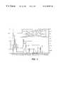
- FIG. 1shows the endpoint traces from this test. The endpoint signal increases rapidly when RF comes on. As “N” increases, the length of time it takes for the endpoint signal to degrade to the baseline increases, showing the clean time is a function of “N”.
- the BCl 3 /CHF 3 WRSwas tested on the 9600PTXTM system using the process conditions for the Al etch, WAC, and WRS steps shown in Table 7.
- the systemwas initially conditioned by cycling 57 blanket resist wafers with the Al etch process conditions.
- the Al etch rate for the conditioned chamberwas measured. Following this the chamber was over cleaned using the WAC process conditions with a 7 minute clean time. The 703 nm endpoint signal was used to verify the clean time was sufficient.
- 29 additional blanket resist waferswere cycled through the system using the Al etch process, but the WAC and WRS steps were used between each wafer.
- the Al etch ratewas then checked again following a WAC and WRS step.
- the etch depth resultsare shown in Table 8. The etch rate following the WAC and WRS was not significantly different than the etch rate of the seasoned chamber (1.6% lower).
- FIG. 2illustrates the profile test wafer structure before etching.
- FIG. 3shows the endpoint trace for a wafer etched following the 2 step recovery process.
- the endpoint traceclosely matches the trace of a wafer etched in a resist conditioned chamber.
- the etch rates through the BARC, Ti and TiN layersmatch the etch rates of such layers in the resist conditioned chamber. All wafers etched following the 2 step recovery had similar traces.
- Step 150 mt/700 W TCP TM/37 sccm CHF 3 /15 sccm BCl 3 /“X” seconds
- Step 215 mt/450 W TCP TM/“Y”.
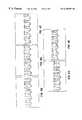
- FIGS. 4A-E and 5 A-Eshow the etch profiles from wafers etched as part of the WAC and WRS matrix compared to the result of etching in a resist conditioned chamber.
- FIGS. 4A, 4 B, 4 C and 4 Dare photomicrographs taken from center locations of wafers 16 , 18 , 17 and 19 , respectively wherein step 1 was run for 30, 20, 20 and 30 seconds respectively, step 2 was run for 15, 15, 7 and 7 seconds respectively, the BCl 3 flow rate was 15, 30, 15 and 30 sccm respectively, the Cl 2 flow rate was 45, 30, 45 and 30 sccm respectively and the RO x was 7154, 7227, 7576 and 7593 Angstroms respectively, FIG.
- FIGS. 5A, 5 B, 5 C and 5 Dare photomicrographs taken from edge locations of wafers 16 , 18 , 17 and 19 , respectively wherein step 1 was run for 30, 20, 20 and 30 seconds respectively, step 2 was run for 15, 15, 7 and 7 seconds respectively, the BCl 3 flow rate was 15, 30 15 and 30 sccm respectively, the Cl 2 flow rate was 45, 30, 45 and 30 sccm respectively and the RO x was 7154, 7227, 7576 and 7593 Angstroms respectively.
- FIG. 5A, 5 B, 5 C and 5 Dare photomicrographs taken from edge locations of wafers 16 , 18 , 17 and 19 , respectively wherein step 1 was run for 30, 20, 20 and 30 seconds respectively, step 2 was run for 15, 15, 7 and 7 seconds respectively, the BCl 3 flow rate was 15, 30 15 and 30 sccm respectively, the Cl 2 flow rate was 45, 30, 45 and 30 sccm respectively and the RO x was 7154, 7227, 7576 and 7593 Angstroms respectively.
- 5Eis a photomicrograph taken from an edge location of wafer 13 etched in a conditioned chamber wherein RO x was 7506 Angstroms. The differences in etch profile between the wafers is subtle in most cases showing that the 2 step recovery process has a reasonable process window. Some notable trends from the matrix include:
- a chlorine base second recovery stepimproves the etch profile recovery.
- the effectis stronger for a short first recovery step time (see wafer 17).
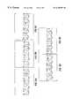
- FIGS. 6A-Fshow additional SEMs comparing the result of wafer 19 to the conditioned chamber result.
- FIG. 6Ashows a center location
- FIG. 6Bshows an edge location
- FIG. 6Cshows an edge location
- FIG. 6Dshows a center location
- FIG. 6Eshows an edge location
- FIG. 6Fshows an edge location. Note in these SEMs the profile of isolated features is also reproduced, and the resist profile and sidewall deposition are matched by the 2 step recovery process as well.
- Process recovery for etching aluminum after WACrequires that a proper balance be achieved between organic deposition in the chamber and chlorination of the chamber walls.
- Process recovery for the CHF 3 additive etch processwhere the etch profile is more sensitive to chemistry balance has been demonstrated.
- the WRS matrixshows that a 2 step recovery process can be tuned to balance the organic and chlorinated composition in the chamber to a “conditioned” state following the WAC.
Landscapes
- Chemical & Material Sciences (AREA)
- Engineering & Computer Science (AREA)
- Plasma & Fusion (AREA)
- Analytical Chemistry (AREA)
- Physics & Mathematics (AREA)
- General Chemical & Material Sciences (AREA)
- Public Health (AREA)
- Epidemiology (AREA)
- Health & Medical Sciences (AREA)
- Chemical Kinetics & Catalysis (AREA)
- Materials Engineering (AREA)
- Mechanical Engineering (AREA)
- Metallurgy (AREA)
- Organic Chemistry (AREA)
- Drying Of Semiconductors (AREA)
- Chemical Vapour Deposition (AREA)
Abstract
Description
During processing of semiconductor wafers it is conventional to carry out periodic in-situ cleaning of plasma etch and CVD reactors. U.S. Pat. No. 5,129,958 discloses a method for cleaning a CVD deposition chamber in a semiconductor wafer processing apparatus wherein fluorine residues in the chamber, left from a prior fluorine plasma cleaning step, are contacted with one or more reducing gases such as silane (SiH4), ammonia, hydrogen, phosphine (PH3), diborine (B2H6), and arsine (AsH3). Another technique for cleaning and conditioning interior surfaces of plasma CVD reactors is disclosed in commonly owned U.S. Pat. No. 5,647,953, the subject matter of which is hereby incorporated by reference. In the past these cleans were done with a wafer in the chamber to cover the electrode, but it has become more common to do waterless cleans.
Other techniques for cleaning plasma reaction chambers are disclosed in commonly owned U.S. Pat. No. 5,356,478; in U.S. Pat. Nos. 4,657,616; 4,786,352; 4,816,113; 4,842,683, 4,857,139; 5,006,192; 5,129,958; 5,158,644 and 5,207,836 and Japanese Laid-Open Patent Publication Nos. 57-201016; 61-250185, 62-214175, 63-267430 and 3-62520. For instance, in order to remove SiOxdeposits, a fluorine-containing gas energized into a plasma has been used to clean interior surfaces of the chamber. Fluorine residues remaining after the reactor cleaning can be removed by passing a reducing gas such as hydrogen (H2), silane (SiH4), ammonia (NH4), phosphine (PH3), biborine (B2H6) or arsine (AsH3) through the reactor.
Chamber conditioning processes are also commonly used where a wafer is placed in the chamber to protect the electrode during conditioning. These conditioning processes are very common for deposition reactors following plasma cleans, and are also common for etch reactors following wet cleans. Sometimes the wafer has a deposited film on it which aids in the conditioning process. As an example, resist coated wafers have commonly been used to accelerate conditioning. Such conditioning steps may use process conditions without bottom electrode power to season the chamber walls.
A problem with using conditioning wafers season the plasma chamber to obtain reproducible process conditions when processing production wafers is that such conditioning wafers add cost and cause slowdown in production. Accordingly, it would be desirable for a conditioning treatment which is more economical in terms of cost and production efficients
FIG. 1 shows 703 nm emission data during a waferless autoclean process in accordance with the invention;
FIG. 2 depicts a pre-etch structure of 0.25 μm profile test wafers;
FIG. 3 is a comparison of profile wafer endpoint traces following chamber conditioning with resist wafers and following the waferless autoclean process in accordance with the invention;
FIGS. 4a,4b,4c,4dare photomicrographs of etched structures after waferless autoclean process and waferless recovery steps in accordance with the invention and FIG. 4eis a photomicrograph of an etched structure processed in a chamber conditioned with resist wafers;
FIGS. 5a,5b,5c,5dare photomicrographs of etched structures after waterless autoclean process and waferless recovery steps in accordance with the invention and FIG. 5eis a photomicrograph of an etched structure processed in a chamber conditioned with resist wafers; and
FIGS. 6a,6b, and6care photomicrographs of etched structures after waterless autoclean process and waferless recovery steps in accordance with the invention and FIGS. 6d,6e, and6fare photoinicrographs of etched structures processed in a chamber conditioned with resist wafers.
This invention provides a method of cleaning and conditioning a plasma reaction chamber in which substrates are processed, comprising the steps of cleaning the plasma reaction chamber so as to remove deposits built up on surfaces within the chamber, introducing a conditioning gas comprising a fluorine-containing gas and a carbon-containing gas into the chamber, energizing the conditioning gas into a plasmastate, depositing a polymer coating on interior surfaces of the chamber, and processing a substrate in the chamber after the depositing step. The term “polymer” coating is intended to describe organic films which may contain etch or deposition by-products.
According to a preferred embodiment of the invention, the energizing step is carried out by exposing the conditioning gas to an inductive field generated by resonating a radio frequency current in an RF antenna coil, the RF antenna coil being disposed external to the chamber, proximate to a dielectric shield which forms a part of an enclosure of the chamber. Further, the cleaning step can be carried out by opening the chamber and performing a wet clean or the cleaning step can be carried out by introducing a cleaning gas into the chamber, energizing the cleaning gas into a plasma state, and contacting the interior surfaces with the plasma to remove the deposits. In the preferred method, the conditioning step is carried out while the chamber does not contain a substrate therein and/or the substrate comprises a production wafer and the processing step is carried out without processing conditioning wafers in the chamber prior to processing the production wafer. Also, the conditioning step can be carried out without applying power to an RF biasing electrode of a substrate support on which the substrate is supported during the processing step.
In cleaning an aluminum etch reactor, the conditioning gas can further comprise a chlorine-containing gas so that the polymer deposited in the depositing step will include chlorine therein and the processing step comprises etching an aluminum layer on the production wafer. In such a case, the conditioning gas can include Cl2, BCl3, CCl4SiCl4or mixture thereof. For example, the conditioning step can be carried out in one or more steps using CHF3, BCl3and/or Cl2as the conditioning gas. The chamber pressure during the conditioning step can be in the range of from about 5 to 80 mTorr and/or a plasma generating antenna can be supplied 200 to 1000 Watts during the conditioning step.
This invention provides an economical method of cleaning and conditioning a plasma reaction chamber in which substrates are processed. The method includes cleaning the plasma reaction chamber so as to remove deposits built up on surfaces within the chamber, introducing a conditioning gas comprising a fluorine-containing gas and a carbon-containing gas into the chamber, energizing the conditioning gas into a plasma, depositing a polymer coating formed by the plasma on interior surfaces of the chamber, and processing a substrate in the chamber after the depositing step.
In a preferred embodiment, the invention provides a waferless plasma clean recovery process for conditioning chambers used for plasma etching an aluminum film stack. The process for plasma etching of Al produces a by-product which deposits throughout the reactor. Eventually this by-product reaches a thickness where it no longer sticks to the reactor wall and particles are shed which contaminate the substrate being etched. When this happens, the reactor must be opened and cleaned with a wet clean process.
The process of preparing a reactor for cleaning, along with the actual clean process and the steps required to condition the chamber following an open chamber clean can require a substantial amount of time. To maximize productivity in a wafer fab, it is desirable to extend the time between opening the chamber to do such open chamber cleans. One method for doing this has been to run plasma cleans, which are capable of reducing the etch by-product deposited in the chamber resulting in a extended time between open chamber cleans. However, since plasma cleans alter the chamber condition by removing the reactor deposits, there is typically a process shift following the plasma clean. As a result, the aluminum etch rate, etch profiles and feature CDs (critical dimension) can shift outside of the acceptable range for the device being manufactured. If a plasma clean is used, wafers are cycled through the chamber to recondition the walls prior to etching product wafers.
In processes wherein a wafer is needed in the chamber for conditioning, a special wafer type may also be needed. This limits the applicability of plasma clean processes for Al etching in a production environment because it would be disruptive to production flows to have to load special wafers into the chamber and run a conditioning process after a plasma clean. As a result, in production, plasma cleans would not be used and the reactors would need to be opened more frequently for long wet clean procedures. Thus, the reactor availability advantage of using plasma cleans to extend the wet clean time is negated by the burden of reconditioning the chamber with a special wafer type.
The invention provides a process that can be run without a wafer in the chamber to recondition the chamber following a plasma clean. The by-product deposition from Al etching has been shown to contain a large amount of organic material. The deposition is present throughout the etch process and participates in the process by providing a source of sidewall passivation, as well as recombination and adsorption sites for reactant species. The deposition can be cleaned by a plasma containing O2. However this leaves some residual O2in the chamber. Further, the addition of O2to Al etching gases is known to increase the Al etch rates and can have an effect on etch profile results.
To recondition the chamber following a plasma clean, it is desirable to remove or bind the residual O2so that the etch process is not affected. It is also desirable to provide organic deposits that participate in the process the same way that by-product deposition does. In a waferless conditioning process, this must be done without attack of the wafer chuck which is not covered or protected during the process.
The preferred method for doing this is to run a plasma processing using BCl3and CHF3. In an inductively coupled plasma etcher such as the TCP 9600™ etcher available from Lam Research Corporation, the process is run by applying high RF power to the top electrode (TCP™ power) source but without power applied to the bottom electrode which provides an RF substrate bias during wafer processing. This results in low plasma potential and prevents attack of the wafer chuck. BCl3is capable of scavenging residual O2from the chamber while CHF3is a source of deposition of organic materials on the chamber walls. BCl3is also a source of C1 which is present in the etch by-product deposition. Typical process conditions and ranges for a TCP 9600™ etch reactor are shown in Table 1.
| TABLE 1 |
| Process Conditions for the Waferless Recovery Process |
| Pressure | TCP ™ Power | Bias Power | BCl3 | CHF3 | ||
| Typical | 50 mt | 700 | 0 watts | 15 sccm | 37 sccm |
| Range | 10-99 | 400-1200 | 0-5 | 10-30 | 10-60 |
Depending on the Al etch stack and process requirements, a second step of the waferless recovery process may be required. If the Al etch process ends with a step that does not contain CHF3, a final step of the recovery process that eliminates CHF3will improve process recovery. An example of a 2 step waferless recovery process is shown in Table 2.
| TABLE 2 |
| Two Step Waferless Recovery Process |
| TCP ™ | |||||||
| Pressure | Power | Bias Power | BCl3 | Cl2 | CHF3 | ||
| Step 1 | 50 mt | 700 | 0 watts | 15 sccm | 37 | |
| Step | ||||||
| 2 | 15 mt | 450 | 0 watts | 30 sccm | 30 sccm | |
While BCl3was selected for it's O2scavenging capability, other gases such as CCl4and SiCl4would be suitable alternatives. The chlorine concentration could be raised by adding Cl2Likewise, many chlorocarbon, fluorocarbon and CFC gases could easily be substituted for CHF3as a polymer source. Diluent gases such as He and Ar could be added while maintaining an effective process.
The waferless recovery process can be run without special wafer types, eliminating the need for operator intervention. An additional benefit to not a: needing wafers for the recovery process is that there is minimal loss to production time as there is no overhead time used to load a wafer into the chamber for the clean or conditioning step. The direct result of this is a higher availability of the reactor for etching valuable product.
Use of the waterless recovery step following a reactor wet clean has the advantage of reducing, wet clean recovery time as well. For instance, compared to a conditioning process wherein it takes around 90 minutes to run 50 resist wafers through the wet-cleaned chamber, according to the invention the conditioning process can be completed in around 5 minutes or less. Thus, the conditioning process according to the invention can cut the recovery time following a chamber clean by over 50%, and even 80% or higher. Further, the chamber can be conditioned in less time without using or minimizing use of conditioning wafers. Increased availability of the reactor for product, and reduced non-production wafer requirements are both advantageous for increased customer profitability.
Test Data and Results, TCP™ 9600SE™ System
System Baseline
This study was started with a baseline of the 9600 SE™ system. The chamber was wet cleaned, and blanket photoresist (PR) wafers were run to condition the chamber. Aluminum etch rate wafers were run on the conditioned chamber to establish the etch rate target for the waferless recovery process development work. The process etch rate shift due to execution of a long O2waferless autoclean (WAC) was established. Etch rate results from the baseline tests are shown in Table 3.
| TABLE 3 |
| Aluminum Etch Rate Baseline Data Before and After an 8 min. O2WAC |
| Pressure Control | |||
| Average | % Change Due to | Valve Angle (% | |
| Wafer ID | Step Height | Clean | open) |
| Pre clean #1 | 4602 | 36.8 | |
| Pre | 4659 | 36.1 | |
| Post WAC | 5254 | 13.5% | 35.5 |
Chamber/Process Recovery Considerations
Several mechanisms have been proposed to account for the etch rate increase following the WAC. One proposal for etch rate recovery was to use Cl2flow control rather than pressure control valve position to regulate pressure since Al etch rate scales with Cl2flow. The interaction of Cl2with clean and conditioned chamber walls will be different (adsorption, recombination, etc.), and if this affected the net Cl2concentration it is possible that this would be reflected in the chamber pressure for a fixed pressure control valve position.
The addition of small amounts of O2to some aluminum etch processes has also been reported to increase Al etch rate. Residual O2in the chamber was proposed as a possible cause of etch rate increase after WAC. A conditioning process that scavenges residual O2could address this issue.
Cycling resist wafers is a very effective method for chamber conditioning and is the recovery procedure recommended after wet clean. This points to the role of carbon in etch by-product as a significant factor in chamber conditioning. Also, the effectiveness of an O2WAC for chamber cleaning indicated that the chamber walls are conditioned with organic deposits. Use of an organic depositing chemistry for chamber conditioning could address this issue.
The proposed mechanisms were considered and a series of experiments were conducted to determine the significant effects.
For the Cl2flow control option to work, there must be a measurable difference in the pressure for a fixed pressure control valve position before and after the waferless clean. Alternatively, we would expect to see the pressure control valve open wider to maintain a set pressure after the WAC if Cl2flow control could be effective. Table 3 above shows the pressure control valve position before (2 wafers) and after WAC. The change in position is small and, if significant, in the wrong direction for Cl2flow control to be effective for etch rate recovery.
Based on this, the approach investigated for chamber recovery was to look at the feasibility of a waferless recovery step (WRS). With the proposed mechanisms in mind, 3 chemistries were investigated, namely Cl2/BCl3(O2Scavenging), Cl2/CHF3(organic depositing), BCl3/CHF3(combined scavenging and depositing).
To test the possible WRS processes, the system was set up to cycle the blanket resist wafer using the baseline Al etch process with the WAC (12 seconds) and WRS process run between each wafer. The 3 WRS steps tested are shown in Table 4. For each test, 30-40 blanket resist wafers were cycled prior to running an Al etch rate test. Table 5 shows the etch rate results. For a conditioned chamber, the Al etch depth is about 4630 A. The BCl3/CHF3process shows that it is possible to recover the desired Al etch rate following the WAC using a WRS. Assuming etch rate to be a primary indicator of process shift, the feasibility of using a WRS to recover the desired process stability following WAC looks very good.
| TABLE 4 |
| WRS Process Conditions Tested |
| Parameter | Cl2/BCl3 | Cl2/CHF3 | BCl3/CHF3 | ||
| Pressure | 20 mt | 20 mt | 50 mt | ||
| TCP ™ | 700 W | 700 W | 700 W | ||
| Cl2 | 162 sccm | 30 sccm | |||
| BCl3 | 54 sccm | 15 sccm | |||
| CHF3 | 37 sccm | 37 sccm | |||
| Step Time | 8 sec | 15 sec | 20 sec | ||
| TABLE 5 |
| Etch Depth Results for the WRS Process Tests |
| WRS Process | Al Etch Depth | Change From Conditioned Chamber |
| Cl2/BCl3 | 5445 A | 17.6% |
| Cl2/CHF3 | 5300 A | 14.5% |
| BCl3/CHF3 | 4671 A | 0.9% |
Waferless Clean Frequency
An important part of WAC implementation will be selecting a WAC frequency that minimizes throughput impact while maximizing effectiveness at maintaining a clean chamber. The optical emission at 703 nm was determined to be a suitable WAC endpoint indicator. The signal degrades throughout the WAC process and flattens when the chamber has been adequately cleaned.
A series of tests were run to determine how the required WAC time scales with number of wafers (“N”) between WACs. The chamber was cleaned with an extended O2plasma to reach a baseline condition. This was followed by a test where the number of wafers between running the WAC was varied and the 703 nm emission was monitored during the WAC step to determine the time required to clean the chamber. FIG. 1 shows the endpoint traces from this test. The endpoint signal increases rapidly when RF comes on. As “N” increases, the length of time it takes for the endpoint signal to degrade to the baseline increases, showing the clean time is a function of “N”.
Table 6 shows the endpoint time for the WAC vs. “N” as well as the clean time for wafer. Times are shown for the endpoint signal to degrade to baseline as well as degrading to 100 counts above baseline. For these process conditions the unit clean time diminishes as “N” increases from 1-5, however at “N”=10, the unit cleaning time is increasing. This suggests that an optimal clean frequency might be somewhere between 5-20 wafers.
| TABLE 6 | |||||
| 10 wafers | 5 | 3 wafers | 1 wafer | 1 wafer | |
| WAC Endpoint and Unit Clean Time (seconds) vs. WAC Frequency |
| Full WAC | 265 | 71 | 56 | 37 | 38 |
| Emission | 143 | 45 | 40 | 23 | 24 |
| 1 = 100 |
| Unit Clean Time |
| Full WAC | 26.5 | 14.2 | 18.66667 | 37 | 38 |
| Emission | 14.3 | 11.4 | 13.33333 | 23 | 24 |
| 1 = 100 | |||||
WRS Etch Rate Recovery
The BCl3/CHF3WRS was tested on the 9600PTX™ system using the process conditions for the Al etch, WAC, and WRS steps shown in Table 7. The system was initially conditioned by cycling 57 blanket resist wafers with the Al etch process conditions. The Al etch rate for the conditioned chamber was measured. Following this the chamber was over cleaned using the WAC process conditions with a 7 minute clean time. The 703 nm endpoint signal was used to verify the clean time was sufficient. Next, 29 additional blanket resist wafers were cycled through the system using the Al etch process, but the WAC and WRS steps were used between each wafer. The Al etch rate was then checked again following a WAC and WRS step. The etch depth results are shown in Table 8. The etch rate following the WAC and WRS was not significantly different than the etch rate of the seasoned chamber (1.6% lower).
| TABLE 7 |
| Al Etch, WAC, and WRS Process Conditions |
| TCP ™ | Bias | Flows | He | Time | ||
| Process | Pressure | (W) | (W) | (sccm) | Cooling | (S) |
| Cycle | 12 mt | 350 | 78 | 74 Cl2 | 30 BCl3 | 5 CHF3 | 10 T | 65 |
| Al Etch | 12 mt | 350 | 78 | 74 Cl2 | 30 BCl3 | 5 CHF3 | 10 T | 35 |
| Depth | ||||||||
| WAC | 32 mt | 700 | 0 | 500 O2 | 12 | |||
| WRS | 50 mt | 700 | 0 | 15 BCl3 | 37 CHF3 | 20 | ||
| TABLE 8 |
| Al Etch Depth of the Conditioned Chamber |
| and Following the WAC + WRS Process |
| Test Condition | Al Etch Depth | Delta | ||
| Conditioned Chamber | 3835 | |||
| Post WAC + WRS | 3773 | ˜1.6% | ||
Profile Etch Tests
Etch tests were performed to determine the effect of the WAC and WRS on etch profile. FIG. 2 illustrates the profile test wafer structure before etching.
A small matrix was run to evaluate the importance of step time and BCl3:Cl2ratio in the recovery step on etch profile. Table 9 shows the 4 processes run in a ½ factorial matrix. FIG. 3 shows the endpoint trace for a wafer etched following the 2 step recovery process. The endpoint trace closely matches the trace of a wafer etched in a resist conditioned chamber. Further, the etch rates through the BARC, Ti and TiN layers match the etch rates of such layers in the resist conditioned chamber. All wafers etched following the 2 step recovery had similar traces.
| TABLE 9 |
| Baseline Process: |
| Step 1: 50 mt/700 W TCP ™/37 sccm CHF3/15 sccm BCl3/“X” seconds |
| Step 2: 15 mt/450 W TCP ™/“Y”. sccm BCl3/(60-“Y) sccm Cl2/“Z” seconds |
| Matrix | Wafer 16 | Wafer 17 | Wafer 18 | Wafer 19 |
| Step 1 Time (“X”) | 30 sec | 20 sec | 20 sec | 30 |
| Step | ||||
| 2 Time (“Z”) | 15 sec | 7 sec | 15 sec | 7 sec |
| BCl3/Cl2Flows | 15 sccm BCl3 | 15 sccm BCl3 | 30 sccm BCl3 | 20 sccm BCl3 |
| (“Y”)/(60-“Y”) | 45 sccm Cl2 | 45 sccm Cl2 | 30 sccm Cl2 | 30 sccm Cl2 |
FIGS. 4A-E and5A-E show the etch profiles from wafers etched as part of the WAC and WRS matrix compared to the result of etching in a resist conditioned chamber. FIGS. 4A,4B,4C and4D are photomicrographs taken from center locations of wafers16,18,17 and19, respectively wherein step1 was run for 30, 20, 20 and 30 seconds respectively,step 2 was run for 15, 15, 7 and 7 seconds respectively, the BCl3flow rate was 15, 30, 15 and 30 sccm respectively, the Cl2flow rate was 45, 30, 45 and 30 sccm respectively and the ROxwas 7154, 7227, 7576 and 7593 Angstroms respectively, FIG. 4E is a photomicrograph taken from a center location of wafer13 etched in a conditioned chamber wherein ROxwas 7506 Angstroms. FIGS. 5A,5B,5C and5D are photomicrographs taken from edge locations of wafers16,18,17 and19, respectively wherein step1 was run for 30, 20, 20 and 30 seconds respectively,step 2 was run for 15, 15, 7 and 7 seconds respectively, the BCl3flow rate was 15, 30 15 and 30 sccm respectively, the Cl2flow rate was 45, 30, 45 and 30 sccm respectively and the ROxwas 7154, 7227, 7576 and 7593 Angstroms respectively. FIG. 5E is a photomicrograph taken from an edge location of wafer13 etched in a conditioned chamber wherein ROxwas 7506 Angstroms. The differences in etch profile between the wafers is subtle in most cases showing that the 2 step recovery process has a reasonable process window. Some notable trends from the matrix include:
A chlorine base second recovery step improves the etch profile recovery.
Use of a higher % Cl2in the second recovery step appears to result in reduced CD growth in the feature top compared to the reference wafer.
The effect is stronger for a short first recovery step time (see wafer 17).
Use of the longer first recovery step improves process latitude for sidewall smoothness.
Wafers etched with the shorter second step times more closely matched the remaining oxide on the reference wafer.
FIGS. 6A-F show additional SEMs comparing the result of wafer 19 to the conditioned chamber result. FIG. 6A shows a center location, FIG. 6B shows an edge location, FIG. 6C shows an edge location. FIG. 6D shows a center location, FIG. 6E shows an edge location, and FIG. 6F shows an edge location. Note in these SEMs the profile of isolated features is also reproduced, and the resist profile and sidewall deposition are matched by the 2 step recovery process as well.
It appears that running the first recovery step long enough to generate some organic film in the chamber, followed by running a brief chlorine chemistry is sufficient to recover the process after the WAC. The chlorine chemistry step may not be necessary for processes that rely on heavy organic deposition and high bombardment energies to protect the etch sidewall.
Process recovery for etching aluminum after WAC requires that a proper balance be achieved between organic deposition in the chamber and chlorination of the chamber walls. Process recovery for the CHF3additive etch process where the etch profile is more sensitive to chemistry balance has been demonstrated. The WRS matrix shows that a 2 step recovery process can be tuned to balance the organic and chlorinated composition in the chamber to a “conditioned” state following the WAC.
While the invention has been described in detail with reference to specific embodiments thereof, it will be apparent to those skilled in the art that various changes and modifications can be made, and equivalents employed, without departing from the scope of the appended claims.
Claims (21)
1. A method of cleaning and conditioning a plasma reaction chamber in which substrates are processed, comprising the steps of:
cleaning the plasma reaction chamber so as to remove deposits built up on surfaces within the chamber;
conditioning the chamber by introducing a conditioning gas comprising a fluorine-containing gas and a carbon-containing gas into the chamber, energizing the conditioning gas into a plasma and, depositing a polymer coating formed by the plasma on interior surfaces of the chamber, the conditioning step being carried out while the chamber does not contain a substrate therein; and
processing a substrate in the chamber after the conditioning step.
2. The method ofclaim 1 , wherein the energizing step is carried out by exposing the conditioning gas to an inductive field generated by resonating a radio frequency current in an RF antenna coil, the RF antenna coil being disposed external to the chamber, proximate to a dielectric shield which forms a part of an enclosure of the chamber.
3. The method ofclaim 2 , wherein the RF antenna is supplied 200 to 1000 Watts during the conditioning step.
4. The method ofclaim 1 , wherein the conditioning gas further comprises a chlorine-containing gas and the polymer deposited in the depositing step includes chlorine therein.
5. The method ofclaim 1 , wherein the cleaning step is carried out by opening the chamber and performing a wet clean.
6. The method ofclaim 1 , wherein the cleaning step is carried out by introducing a cleaning gas into the chamber, energizing the cleaning gas into a plasma state, and contacting the interior surfaces with the plasma to remove the deposits.
7. The method ofclaim 5 , wherein the plasma cleaning gas converts the deposits on the interior surfaces to gas by-products.
8. The method ofclaim 1 , wherein the substrate comprises a production wafer and the processing step is carried out without processing conditioning wafers in the chamber prior to processing the production wafer.
9. The method ofclaim 1 , wherein the processing step comprises etching an aluminum film stack on the production wafer.
10. The method ofclaim 1 , wherein the conditioning step is carried out without applying power to an RF biasing electrode of a substrate support on which the substrate is supported during the processing step.
11. The method ofclaim 1 , wherein the conditioning gas includes Cl2, BCl3, CCl4, SiCl4or mixture thereof.
12. The method ofclaim 1 , wherein the conditioning gas includes CHF3and BCl3and/or Cl2.
13. The method ofclaim 1 , wherein the chamber pressure during the conditioning step is in the range of from about 5 to 80 mTorr.
14. The method ofclaim 1 , wherein the chamber is a plasma etch chamber.
15. The method ofclaim 14 , further comprising a step of etching aluminum on one or more semiconductor substrates in the chamber prior to the cleaning step, the etching step producing the deposits on the interior surfaces of the chamber.
16. The method ofclaim 14 , wherein the conditioning step is followed by introducing one or more semiconductor substrates into the chamber and etching aluminum on the one or more substrates.
17. The method ofclaim 1 , wherein the conditioning step is performed until an endpoint determined by optical emission or interferometry is reached.
18. The method ofclaim 1 , wherein the conditioning step is carried out in first and second steps, the conditioning gas further including a chlorine-containing gas in the first step and the conditioning gas being fluorine-free in the second step.
19. The method ofclaim 18 , wherein the conditioning gas comprises 1-30 sccm BCl3and 10-60 sccm CHF3in the first step and the conditioning gas comprises 20-60 sccm BCl3and 20-60 sccm Cl2in the second step.
20. The method ofclaim 1 , wherein residual oxygen in the plasma reaction chamber is scavenged by the plasma formed from the conditioning gas.
21. The method ofclaim 1 , wherein an etch rate of a first substrate processed according to an etch recipe in the plasma reaction chamber prior to the cleaning step and an etch rate of a second substrate processed according to the etch recipe in the plasma reaction chamber after the depositing step are substantially equal etch rates.
Priority Applications (9)
| Application Number | Priority Date | Filing Date | Title |
|---|---|---|---|
| US09/469,286US6350697B1 (en) | 1999-12-22 | 1999-12-22 | Method of cleaning and conditioning plasma reaction chamber |
| PCT/US2000/032441WO2001046490A1 (en) | 1999-12-22 | 2000-12-08 | Method of cleaning and conditioning plasma reaction chamber |
| AU20499/01AAU2049901A (en) | 1999-12-22 | 2000-12-08 | Method of cleaning and conditioning plasma reaction chamber |
| DE60042892TDE60042892D1 (en) | 1999-12-22 | 2000-12-08 | Method for purifying and conditioning a plasma reaction chamber |
| CNB008174482ACN1252313C (en) | 1999-12-22 | 2000-12-08 | Method of cleaning and conditioning plasma reaction chamber |
| KR1020027008036AKR100789684B1 (en) | 1999-12-22 | 2000-12-08 | How to Clean and Control Plasma Reaction Chamber |
| JP2001546982AJP4995390B2 (en) | 1999-12-22 | 2000-12-08 | Method for cleaning and conditioning a plasma reaction chamber |
| EP00983789AEP1252361B1 (en) | 1999-12-22 | 2000-12-08 | Method of cleaning and conditioning plasma reaction chamber |
| TW089126728ATW487988B (en) | 1999-12-22 | 2000-12-14 | Method of cleaning and conditioning plasma reaction chamber |
Applications Claiming Priority (1)
| Application Number | Priority Date | Filing Date | Title |
|---|---|---|---|
| US09/469,286US6350697B1 (en) | 1999-12-22 | 1999-12-22 | Method of cleaning and conditioning plasma reaction chamber |
Publications (1)
| Publication Number | Publication Date |
|---|---|
| US6350697B1true US6350697B1 (en) | 2002-02-26 |
Family
ID=23863210
Family Applications (1)
| Application Number | Title | Priority Date | Filing Date |
|---|---|---|---|
| US09/469,286Expired - LifetimeUS6350697B1 (en) | 1999-12-22 | 1999-12-22 | Method of cleaning and conditioning plasma reaction chamber |
Country Status (9)
| Country | Link |
|---|---|
| US (1) | US6350697B1 (en) |
| EP (1) | EP1252361B1 (en) |
| JP (1) | JP4995390B2 (en) |
| KR (1) | KR100789684B1 (en) |
| CN (1) | CN1252313C (en) |
| AU (1) | AU2049901A (en) |
| DE (1) | DE60042892D1 (en) |
| TW (1) | TW487988B (en) |
| WO (1) | WO2001046490A1 (en) |
Cited By (182)
| Publication number | Priority date | Publication date | Assignee | Title |
|---|---|---|---|---|
| US20030017087A1 (en)* | 2001-07-18 | 2003-01-23 | Applied Materials Inc. | Process and apparatus for abatement of by products generated from deposition processes and cleaning of deposition chambers |
| US20030047449A1 (en)* | 2000-08-11 | 2003-03-13 | Applied Materials, Inc. | Method to drive spatially separate resonant structure with spatially distinct plasma secondaries using a single generator and switching elements |
| US6708700B2 (en)* | 2000-03-28 | 2004-03-23 | Asm America | Cleaning of semiconductor processing chambers |
| US20040107907A1 (en)* | 2000-08-11 | 2004-06-10 | Applied Materials, Inc. | Plasma immersion ion implantation system including a plasma source having low dissociation and low minimum plasma voltage |
| US20040107908A1 (en)* | 2002-06-05 | 2004-06-10 | Applied Materials, Inc. | Plasma immersion ion implantation apparatus including an inductively coupled plasma source having low dissociation and low minimum plasma voltage |
| US20040107906A1 (en)* | 2000-08-11 | 2004-06-10 | Applied Materials, Inc. | Plasma immersion ion implantation apparatus including a plasma source having low dissociation and low minimum plasma voltage |
| US20040149218A1 (en)* | 2000-08-11 | 2004-08-05 | Applied Materials, Inc. | Plasma immersion ion implantation process using a capacitively coupled plasma source having low dissociation and low minimum plasma voltage |
| US6776851B1 (en)* | 2001-07-11 | 2004-08-17 | Lam Research Corporation | In-situ cleaning of a polymer coated plasma processing chamber |
| US6797634B2 (en) | 2001-04-20 | 2004-09-28 | Kawasaki Microelectronics, Inc. | Method of conditioning an etching chamber and method of processing semiconductor substrate using the etching chamber |
| US20040200417A1 (en)* | 2002-06-05 | 2004-10-14 | Applied Materials, Inc. | Very low temperature CVD process with independently variable conformality, stress and composition of the CVD layer |
| US20040221869A1 (en)* | 2001-09-28 | 2004-11-11 | Smith Bradley C. | Method of removing PECVD residues of fluorinated plasma using in-situ H2 plasma |
| US20050051272A1 (en)* | 2000-08-11 | 2005-03-10 | Applied Materials, Inc. | Plasma immersion ion implantation process using an inductively coupled plasma source having low dissociation and low minimum plasma voltage |
| US20050106891A1 (en)* | 2003-11-18 | 2005-05-19 | Polinsky William A. | Conditioning of a reaction chamber |
| US20050136604A1 (en)* | 2000-08-10 | 2005-06-23 | Amir Al-Bayati | Semiconductor on insulator vertical transistor fabrication and doping process |
| US6919279B1 (en) | 2002-10-08 | 2005-07-19 | Novellus Systems, Inc. | Endpoint detection for high density plasma (HDP) processes |
| US20050191828A1 (en)* | 2000-08-11 | 2005-09-01 | Applied Materials, Inc. | Method for ion implanting insulator material to reduce dielectric constant |
| US20050191827A1 (en)* | 2000-08-11 | 2005-09-01 | Collins Kenneth S. | Plasma immersion ion implantation process |
| US20050211170A1 (en)* | 2004-03-26 | 2005-09-29 | Applied Materials, Inc. | Chemical vapor deposition plasma reactor having plural ion shower grids |
| US20050214478A1 (en)* | 2004-03-26 | 2005-09-29 | Applied Materials, Inc. | Chemical vapor deposition plasma process using plural ion shower grids |
| US20050211547A1 (en)* | 2004-03-26 | 2005-09-29 | Applied Materials, Inc. | Reactive sputter deposition plasma reactor and process using plural ion shower grids |
| US20050211546A1 (en)* | 2004-03-26 | 2005-09-29 | Applied Materials, Inc. | Reactive sputter deposition plasma process using an ion shower grid |
| US20050214477A1 (en)* | 2004-03-26 | 2005-09-29 | Applied Materials, Inc. | Chemical vapor deposition plasma process using an ion shower grid |
| US20050211171A1 (en)* | 2004-03-26 | 2005-09-29 | Applied Materials, Inc. | Chemical vapor deposition plasma reactor having an ion shower grid |
| US20050230047A1 (en)* | 2000-08-11 | 2005-10-20 | Applied Materials, Inc. | Plasma immersion ion implantation apparatus |
| US20050260354A1 (en)* | 2004-05-20 | 2005-11-24 | Varian Semiconductor Equipment Associates, Inc. | In-situ process chamber preparation methods for plasma ion implantation systems |
| US20060019477A1 (en)* | 2004-07-20 | 2006-01-26 | Hiroji Hanawa | Plasma immersion ion implantation reactor having an ion shower grid |
| US20060019039A1 (en)* | 2004-07-20 | 2006-01-26 | Applied Materials, Inc. | Plasma immersion ion implantation reactor having multiple ion shower grids |
| US20060054183A1 (en)* | 2004-08-27 | 2006-03-16 | Thomas Nowak | Method to reduce plasma damage during cleaning of semiconductor wafer processing chamber |
| US20060081558A1 (en)* | 2000-08-11 | 2006-04-20 | Applied Materials, Inc. | Plasma immersion ion implantation process |
| US20060088655A1 (en)* | 2004-10-23 | 2006-04-27 | Applied Materials, Inc. | RF measurement feedback control and diagnostics for a plasma immersion ion implantation reactor |
| US20060090773A1 (en)* | 2004-11-04 | 2006-05-04 | Applied Materials, Inc. | Sulfur hexafluoride remote plasma source clean |
| US7094670B2 (en) | 2000-08-11 | 2006-08-22 | Applied Materials, Inc. | Plasma immersion ion implantation process |
| US7109098B1 (en) | 2005-05-17 | 2006-09-19 | Applied Materials, Inc. | Semiconductor junction formation process including low temperature plasma deposition of an optical absorption layer and high speed optical annealing |
| US20060260545A1 (en)* | 2005-05-17 | 2006-11-23 | Kartik Ramaswamy | Low temperature absorption layer deposition and high speed optical annealing system |
| US20060263540A1 (en)* | 2005-05-17 | 2006-11-23 | Kartik Ramaswamy | Process for low temperature plasma deposition of an optical absorption layer and high speed optical annealing |
| US20060264060A1 (en)* | 2005-05-17 | 2006-11-23 | Kartik Ramaswamy | Low temperature plasma deposition process for carbon layer deposition |
| US20070032095A1 (en)* | 2005-08-08 | 2007-02-08 | Applied Materials, Inc. | Copper conductor annealing process employing high speed optical annealing with a low temperature-deposited optical absorber layer |
| US20070032004A1 (en)* | 2005-08-08 | 2007-02-08 | Applied Materials, Inc. | Copper barrier reflow process employing high speed optical annealing |
| US20070032054A1 (en)* | 2005-08-08 | 2007-02-08 | Applied Materials, Inc. | Semiconductor substrate process using a low temperature deposited carbon-containing hard mask |
| US20070032082A1 (en)* | 2005-08-08 | 2007-02-08 | Applied Materials, Inc. | Semiconductor substrate process using an optically writable carbon-containing mask |
| US20070042580A1 (en)* | 2000-08-10 | 2007-02-22 | Amir Al-Bayati | Ion implanted insulator material with reduced dielectric constant |
| US7204913B1 (en)* | 2002-06-28 | 2007-04-17 | Lam Research Corporation | In-situ pre-coating of plasma etch chamber for improved productivity and chamber condition control |
| US20070235058A1 (en)* | 2006-04-10 | 2007-10-11 | Daniel Harrington | System and method for removing residue from a wafer processing chamber using sound waves |
| US20080075834A1 (en)* | 2004-10-23 | 2008-03-27 | Kartik Ramaswamy | Dosimetry using optical emission spectroscopy/residual gas analyzer in conjuntion with ion current |
| US20080173237A1 (en)* | 2007-01-19 | 2008-07-24 | Collins Kenneth S | Plasma Immersion Chamber |
| US20080188013A1 (en)* | 2007-02-06 | 2008-08-07 | Seon-Mee Cho | In-situ dose monitoring using optical emission spectroscopy |
| US20080257863A1 (en)* | 2003-08-06 | 2008-10-23 | Hiroyuki Kitsunai | Plasma processing apparatus and method for stabilizing inner wall of processing chamber |
| US7479456B2 (en) | 2004-08-26 | 2009-01-20 | Applied Materials, Inc. | Gasless high voltage high contact force wafer contact-cooling electrostatic chuck |
| US20100010658A1 (en)* | 2008-07-11 | 2010-01-14 | Tokyo Electron Limited | Control device and control method of plasma processing system, and storage medium storing control program |
| US7713757B2 (en) | 2008-03-14 | 2010-05-11 | Applied Materials, Inc. | Method for measuring dopant concentration during plasma ion implantation |
| US20110295554A1 (en)* | 2010-05-26 | 2011-12-01 | Samsung Electronics Co., Ltd. | Equipment For Manufacturing Semiconductor Device And Seasoning Process Method Of The Same |
| WO2015094495A1 (en)* | 2013-12-18 | 2015-06-25 | Applied Materials, Inc. | Procedure for etch rate consistency |
| US9245762B2 (en)* | 2013-12-02 | 2016-01-26 | Applied Materials, Inc. | Procedure for etch rate consistency |
| US9269590B2 (en) | 2014-04-07 | 2016-02-23 | Applied Materials, Inc. | Spacer formation |
| US9287134B2 (en) | 2014-01-17 | 2016-03-15 | Applied Materials, Inc. | Titanium oxide etch |
| US9287095B2 (en) | 2013-12-17 | 2016-03-15 | Applied Materials, Inc. | Semiconductor system assemblies and methods of operation |
| US9293568B2 (en) | 2014-01-27 | 2016-03-22 | Applied Materials, Inc. | Method of fin patterning |
| US9299538B2 (en) | 2014-03-20 | 2016-03-29 | Applied Materials, Inc. | Radial waveguide systems and methods for post-match control of microwaves |
| US9299537B2 (en) | 2014-03-20 | 2016-03-29 | Applied Materials, Inc. | Radial waveguide systems and methods for post-match control of microwaves |
| US9299575B2 (en) | 2014-03-17 | 2016-03-29 | Applied Materials, Inc. | Gas-phase tungsten etch |
| US9299583B1 (en) | 2014-12-05 | 2016-03-29 | Applied Materials, Inc. | Aluminum oxide selective etch |
| US9309598B2 (en) | 2014-05-28 | 2016-04-12 | Applied Materials, Inc. | Oxide and metal removal |
| US9324576B2 (en) | 2010-05-27 | 2016-04-26 | Applied Materials, Inc. | Selective etch for silicon films |
| US9343272B1 (en) | 2015-01-08 | 2016-05-17 | Applied Materials, Inc. | Self-aligned process |
| US9349605B1 (en) | 2015-08-07 | 2016-05-24 | Applied Materials, Inc. | Oxide etch selectivity systems and methods |
| US9355856B2 (en) | 2014-09-12 | 2016-05-31 | Applied Materials, Inc. | V trench dry etch |
| US9355863B2 (en) | 2012-12-18 | 2016-05-31 | Applied Materials, Inc. | Non-local plasma oxide etch |
| US9355862B2 (en) | 2014-09-24 | 2016-05-31 | Applied Materials, Inc. | Fluorine-based hardmask removal |
| US9368364B2 (en) | 2014-09-24 | 2016-06-14 | Applied Materials, Inc. | Silicon etch process with tunable selectivity to SiO2 and other materials |
| US9373522B1 (en) | 2015-01-22 | 2016-06-21 | Applied Mateials, Inc. | Titanium nitride removal |
| US9373517B2 (en) | 2012-08-02 | 2016-06-21 | Applied Materials, Inc. | Semiconductor processing with DC assisted RF power for improved control |
| US9378978B2 (en) | 2014-07-31 | 2016-06-28 | Applied Materials, Inc. | Integrated oxide recess and floating gate fin trimming |
| US9378969B2 (en) | 2014-06-19 | 2016-06-28 | Applied Materials, Inc. | Low temperature gas-phase carbon removal |
| US9384997B2 (en) | 2012-11-20 | 2016-07-05 | Applied Materials, Inc. | Dry-etch selectivity |
| US9385028B2 (en) | 2014-02-03 | 2016-07-05 | Applied Materials, Inc. | Air gap process |
| US9390937B2 (en) | 2012-09-20 | 2016-07-12 | Applied Materials, Inc. | Silicon-carbon-nitride selective etch |
| US9396989B2 (en) | 2014-01-27 | 2016-07-19 | Applied Materials, Inc. | Air gaps between copper lines |
| US9406523B2 (en) | 2014-06-19 | 2016-08-02 | Applied Materials, Inc. | Highly selective doped oxide removal method |
| US9412608B2 (en) | 2012-11-30 | 2016-08-09 | Applied Materials, Inc. | Dry-etch for selective tungsten removal |
| US9418858B2 (en) | 2011-10-07 | 2016-08-16 | Applied Materials, Inc. | Selective etch of silicon by way of metastable hydrogen termination |
| US9425058B2 (en) | 2014-07-24 | 2016-08-23 | Applied Materials, Inc. | Simplified litho-etch-litho-etch process |
| US9437451B2 (en) | 2012-09-18 | 2016-09-06 | Applied Materials, Inc. | Radical-component oxide etch |
| US9449845B2 (en) | 2012-12-21 | 2016-09-20 | Applied Materials, Inc. | Selective titanium nitride etching |
| US9449846B2 (en) | 2015-01-28 | 2016-09-20 | Applied Materials, Inc. | Vertical gate separation |
| US9449850B2 (en) | 2013-03-15 | 2016-09-20 | Applied Materials, Inc. | Processing systems and methods for halide scavenging |
| US9472417B2 (en) | 2013-11-12 | 2016-10-18 | Applied Materials, Inc. | Plasma-free metal etch |
| US9478432B2 (en) | 2014-09-25 | 2016-10-25 | Applied Materials, Inc. | Silicon oxide selective removal |
| US9493879B2 (en) | 2013-07-12 | 2016-11-15 | Applied Materials, Inc. | Selective sputtering for pattern transfer |
| US9496167B2 (en) | 2014-07-31 | 2016-11-15 | Applied Materials, Inc. | Integrated bit-line airgap formation and gate stack post clean |
| US9499898B2 (en) | 2014-03-03 | 2016-11-22 | Applied Materials, Inc. | Layered thin film heater and method of fabrication |
| US9502258B2 (en) | 2014-12-23 | 2016-11-22 | Applied Materials, Inc. | Anisotropic gap etch |
| US9553102B2 (en) | 2014-08-19 | 2017-01-24 | Applied Materials, Inc. | Tungsten separation |
| US9576809B2 (en) | 2013-11-04 | 2017-02-21 | Applied Materials, Inc. | Etch suppression with germanium |
| US9607856B2 (en) | 2013-03-05 | 2017-03-28 | Applied Materials, Inc. | Selective titanium nitride removal |
| US9613819B2 (en)* | 2014-06-06 | 2017-04-04 | Taiwan Semiconductor Manufacturing Company, Ltd. | Process chamber, method of preparing a process chamber, and method of operating a process chamber |
| US9659753B2 (en) | 2014-08-07 | 2017-05-23 | Applied Materials, Inc. | Grooved insulator to reduce leakage current |
| US9691645B2 (en) | 2015-08-06 | 2017-06-27 | Applied Materials, Inc. | Bolted wafer chuck thermal management systems and methods for wafer processing systems |
| US9721789B1 (en) | 2016-10-04 | 2017-08-01 | Applied Materials, Inc. | Saving ion-damaged spacers |
| US9728437B2 (en) | 2015-02-03 | 2017-08-08 | Applied Materials, Inc. | High temperature chuck for plasma processing systems |
| US9741593B2 (en) | 2015-08-06 | 2017-08-22 | Applied Materials, Inc. | Thermal management systems and methods for wafer processing systems |
| US9768034B1 (en) | 2016-11-11 | 2017-09-19 | Applied Materials, Inc. | Removal methods for high aspect ratio structures |
| US9773648B2 (en) | 2013-08-30 | 2017-09-26 | Applied Materials, Inc. | Dual discharge modes operation for remote plasma |
| US9842744B2 (en) | 2011-03-14 | 2017-12-12 | Applied Materials, Inc. | Methods for etch of SiN films |
| US9865484B1 (en) | 2016-06-29 | 2018-01-09 | Applied Materials, Inc. | Selective etch using material modification and RF pulsing |
| US9881805B2 (en) | 2015-03-02 | 2018-01-30 | Applied Materials, Inc. | Silicon selective removal |
| US9885117B2 (en) | 2014-03-31 | 2018-02-06 | Applied Materials, Inc. | Conditioned semiconductor system parts |
| US9887096B2 (en) | 2012-09-17 | 2018-02-06 | Applied Materials, Inc. | Differential silicon oxide etch |
| US9934942B1 (en) | 2016-10-04 | 2018-04-03 | Applied Materials, Inc. | Chamber with flow-through source |
| US9947549B1 (en) | 2016-10-10 | 2018-04-17 | Applied Materials, Inc. | Cobalt-containing material removal |
| US9978564B2 (en) | 2012-09-21 | 2018-05-22 | Applied Materials, Inc. | Chemical control features in wafer process equipment |
| US10026621B2 (en) | 2016-11-14 | 2018-07-17 | Applied Materials, Inc. | SiN spacer profile patterning |
| US10043674B1 (en) | 2017-08-04 | 2018-08-07 | Applied Materials, Inc. | Germanium etching systems and methods |
| US10043684B1 (en) | 2017-02-06 | 2018-08-07 | Applied Materials, Inc. | Self-limiting atomic thermal etching systems and methods |
| US10049891B1 (en) | 2017-05-31 | 2018-08-14 | Applied Materials, Inc. | Selective in situ cobalt residue removal |
| US10062585B2 (en) | 2016-10-04 | 2018-08-28 | Applied Materials, Inc. | Oxygen compatible plasma source |
| US10062587B2 (en) | 2012-07-18 | 2018-08-28 | Applied Materials, Inc. | Pedestal with multi-zone temperature control and multiple purge capabilities |
| US10062575B2 (en) | 2016-09-09 | 2018-08-28 | Applied Materials, Inc. | Poly directional etch by oxidation |
| US10062578B2 (en) | 2011-03-14 | 2018-08-28 | Applied Materials, Inc. | Methods for etch of metal and metal-oxide films |
| US10062579B2 (en) | 2016-10-07 | 2018-08-28 | Applied Materials, Inc. | Selective SiN lateral recess |
| US10128133B1 (en) | 2017-06-30 | 2018-11-13 | Infineon Technologies Austria Ag | Method of conditioning an etch chamber for contaminant free etching of a semiconductor device |
| US10128086B1 (en) | 2017-10-24 | 2018-11-13 | Applied Materials, Inc. | Silicon pretreatment for nitride removal |
| US10163696B2 (en) | 2016-11-11 | 2018-12-25 | Applied Materials, Inc. | Selective cobalt removal for bottom up gapfill |
| US10170336B1 (en) | 2017-08-04 | 2019-01-01 | Applied Materials, Inc. | Methods for anisotropic control of selective silicon removal |
| US10224210B2 (en) | 2014-12-09 | 2019-03-05 | Applied Materials, Inc. | Plasma processing system with direct outlet toroidal plasma source |
| US10242908B2 (en) | 2016-11-14 | 2019-03-26 | Applied Materials, Inc. | Airgap formation with damage-free copper |
| US10256079B2 (en) | 2013-02-08 | 2019-04-09 | Applied Materials, Inc. | Semiconductor processing systems having multiple plasma configurations |
| US10256112B1 (en) | 2017-12-08 | 2019-04-09 | Applied Materials, Inc. | Selective tungsten removal |
| US10283321B2 (en) | 2011-01-18 | 2019-05-07 | Applied Materials, Inc. | Semiconductor processing system and methods using capacitively coupled plasma |
| US10283324B1 (en) | 2017-10-24 | 2019-05-07 | Applied Materials, Inc. | Oxygen treatment for nitride etching |
| US10297458B2 (en) | 2017-08-07 | 2019-05-21 | Applied Materials, Inc. | Process window widening using coated parts in plasma etch processes |
| US10319649B2 (en) | 2017-04-11 | 2019-06-11 | Applied Materials, Inc. | Optical emission spectroscopy (OES) for remote plasma monitoring |
| US10319600B1 (en) | 2018-03-12 | 2019-06-11 | Applied Materials, Inc. | Thermal silicon etch |
| US10319739B2 (en) | 2017-02-08 | 2019-06-11 | Applied Materials, Inc. | Accommodating imperfectly aligned memory holes |
| US10354889B2 (en) | 2017-07-17 | 2019-07-16 | Applied Materials, Inc. | Non-halogen etching of silicon-containing materials |
| US10403507B2 (en) | 2017-02-03 | 2019-09-03 | Applied Materials, Inc. | Shaped etch profile with oxidation |
| US10424485B2 (en) | 2013-03-01 | 2019-09-24 | Applied Materials, Inc. | Enhanced etching processes using remote plasma sources |
| US10431429B2 (en) | 2017-02-03 | 2019-10-01 | Applied Materials, Inc. | Systems and methods for radial and azimuthal control of plasma uniformity |
| US10468267B2 (en) | 2017-05-31 | 2019-11-05 | Applied Materials, Inc. | Water-free etching methods |
| US10490418B2 (en) | 2014-10-14 | 2019-11-26 | Applied Materials, Inc. | Systems and methods for internal surface conditioning assessment in plasma processing equipment |
| US10490406B2 (en) | 2018-04-10 | 2019-11-26 | Appled Materials, Inc. | Systems and methods for material breakthrough |
| US10497573B2 (en) | 2018-03-13 | 2019-12-03 | Applied Materials, Inc. | Selective atomic layer etching of semiconductor materials |
| US10504700B2 (en) | 2015-08-27 | 2019-12-10 | Applied Materials, Inc. | Plasma etching systems and methods with secondary plasma injection |
| US10504754B2 (en) | 2016-05-19 | 2019-12-10 | Applied Materials, Inc. | Systems and methods for improved semiconductor etching and component protection |
| US10522371B2 (en) | 2016-05-19 | 2019-12-31 | Applied Materials, Inc. | Systems and methods for improved semiconductor etching and component protection |
| US10541184B2 (en) | 2017-07-11 | 2020-01-21 | Applied Materials, Inc. | Optical emission spectroscopic techniques for monitoring etching |
| US10541246B2 (en) | 2017-06-26 | 2020-01-21 | Applied Materials, Inc. | 3D flash memory cells which discourage cross-cell electrical tunneling |
| US10546729B2 (en) | 2016-10-04 | 2020-01-28 | Applied Materials, Inc. | Dual-channel showerhead with improved profile |
| US10566206B2 (en) | 2016-12-27 | 2020-02-18 | Applied Materials, Inc. | Systems and methods for anisotropic material breakthrough |
| US10573527B2 (en) | 2018-04-06 | 2020-02-25 | Applied Materials, Inc. | Gas-phase selective etching systems and methods |
| US10573496B2 (en) | 2014-12-09 | 2020-02-25 | Applied Materials, Inc. | Direct outlet toroidal plasma source |
| US10593560B2 (en) | 2018-03-01 | 2020-03-17 | Applied Materials, Inc. | Magnetic induction plasma source for semiconductor processes and equipment |
| US10593523B2 (en) | 2014-10-14 | 2020-03-17 | Applied Materials, Inc. | Systems and methods for internal surface conditioning in plasma processing equipment |
| US10615047B2 (en) | 2018-02-28 | 2020-04-07 | Applied Materials, Inc. | Systems and methods to form airgaps |
| US10629473B2 (en) | 2016-09-09 | 2020-04-21 | Applied Materials, Inc. | Footing removal for nitride spacer |
| US10672642B2 (en) | 2018-07-24 | 2020-06-02 | Applied Materials, Inc. | Systems and methods for pedestal configuration |
| US10679870B2 (en) | 2018-02-15 | 2020-06-09 | Applied Materials, Inc. | Semiconductor processing chamber multistage mixing apparatus |
| US10699879B2 (en) | 2018-04-17 | 2020-06-30 | Applied Materials, Inc. | Two piece electrode assembly with gap for plasma control |
| US10727080B2 (en) | 2017-07-07 | 2020-07-28 | Applied Materials, Inc. | Tantalum-containing material removal |
| US10755941B2 (en) | 2018-07-06 | 2020-08-25 | Applied Materials, Inc. | Self-limiting selective etching systems and methods |
| US10854426B2 (en) | 2018-01-08 | 2020-12-01 | Applied Materials, Inc. | Metal recess for semiconductor structures |
| US10872778B2 (en) | 2018-07-06 | 2020-12-22 | Applied Materials, Inc. | Systems and methods utilizing solid-phase etchants |
| US10886137B2 (en) | 2018-04-30 | 2021-01-05 | Applied Materials, Inc. | Selective nitride removal |
| US10892198B2 (en) | 2018-09-14 | 2021-01-12 | Applied Materials, Inc. | Systems and methods for improved performance in semiconductor processing |
| US10903054B2 (en) | 2017-12-19 | 2021-01-26 | Applied Materials, Inc. | Multi-zone gas distribution systems and methods |
| US10920320B2 (en) | 2017-06-16 | 2021-02-16 | Applied Materials, Inc. | Plasma health determination in semiconductor substrate processing reactors |
| US10920319B2 (en) | 2019-01-11 | 2021-02-16 | Applied Materials, Inc. | Ceramic showerheads with conductive electrodes |
| US10943834B2 (en) | 2017-03-13 | 2021-03-09 | Applied Materials, Inc. | Replacement contact process |
| US10964512B2 (en) | 2018-02-15 | 2021-03-30 | Applied Materials, Inc. | Semiconductor processing chamber multistage mixing apparatus and methods |
| US11049755B2 (en) | 2018-09-14 | 2021-06-29 | Applied Materials, Inc. | Semiconductor substrate supports with embedded RF shield |
| US11062887B2 (en) | 2018-09-17 | 2021-07-13 | Applied Materials, Inc. | High temperature RF heater pedestals |
| US11121002B2 (en) | 2018-10-24 | 2021-09-14 | Applied Materials, Inc. | Systems and methods for etching metals and metal derivatives |
| US11239061B2 (en) | 2014-11-26 | 2022-02-01 | Applied Materials, Inc. | Methods and systems to enhance process uniformity |
| US11257693B2 (en) | 2015-01-09 | 2022-02-22 | Applied Materials, Inc. | Methods and systems to improve pedestal temperature control |
| US11276590B2 (en) | 2017-05-17 | 2022-03-15 | Applied Materials, Inc. | Multi-zone semiconductor substrate supports |
| US11276559B2 (en) | 2017-05-17 | 2022-03-15 | Applied Materials, Inc. | Semiconductor processing chamber for multiple precursor flow |
| US11328909B2 (en) | 2017-12-22 | 2022-05-10 | Applied Materials, Inc. | Chamber conditioning and removal processes |
| US11417534B2 (en) | 2018-09-21 | 2022-08-16 | Applied Materials, Inc. | Selective material removal |
| US11437242B2 (en) | 2018-11-27 | 2022-09-06 | Applied Materials, Inc. | Selective removal of silicon-containing materials |
| US11594428B2 (en) | 2015-02-03 | 2023-02-28 | Applied Materials, Inc. | Low temperature chuck for plasma processing systems |
| US11682560B2 (en) | 2018-10-11 | 2023-06-20 | Applied Materials, Inc. | Systems and methods for hafnium-containing film removal |
| US11721527B2 (en) | 2019-01-07 | 2023-08-08 | Applied Materials, Inc. | Processing chamber mixing systems |
| US12340979B2 (en) | 2017-05-17 | 2025-06-24 | Applied Materials, Inc. | Semiconductor processing chamber for improved precursor flow |
Families Citing this family (28)
| Publication number | Priority date | Publication date | Assignee | Title |
|---|---|---|---|---|
| KR20030078550A (en)* | 2002-03-30 | 2003-10-08 | 주식회사 하이닉스반도체 | Method for cleaning of chamber |
| US6838114B2 (en) | 2002-05-24 | 2005-01-04 | Micron Technology, Inc. | Methods for controlling gas pulsing in processes for depositing materials onto micro-device workpieces |
| US6955725B2 (en) | 2002-08-15 | 2005-10-18 | Micron Technology, Inc. | Reactors with isolated gas connectors and methods for depositing materials onto micro-device workpieces |
| US20040134427A1 (en)* | 2003-01-09 | 2004-07-15 | Derderian Garo J. | Deposition chamber surface enhancement and resulting deposition chambers |
| US7335396B2 (en) | 2003-04-24 | 2008-02-26 | Micron Technology, Inc. | Methods for controlling mass flow rates and pressures in passageways coupled to reaction chambers and systems for depositing material onto microfeature workpieces in reaction chambers |
| US7235138B2 (en) | 2003-08-21 | 2007-06-26 | Micron Technology, Inc. | Microfeature workpiece processing apparatus and methods for batch deposition of materials on microfeature workpieces |
| US7344755B2 (en) | 2003-08-21 | 2008-03-18 | Micron Technology, Inc. | Methods and apparatus for processing microfeature workpieces; methods for conditioning ALD reaction chambers |
| US7422635B2 (en) | 2003-08-28 | 2008-09-09 | Micron Technology, Inc. | Methods and apparatus for processing microfeature workpieces, e.g., for depositing materials on microfeature workpieces |
| CN1332064C (en)* | 2003-09-03 | 2007-08-15 | 统宝光电股份有限公司 | Method for reducing fluorine residue in chamber of deposition reaction chamber |
| US7056806B2 (en) | 2003-09-17 | 2006-06-06 | Micron Technology, Inc. | Microfeature workpiece processing apparatus and methods for controlling deposition of materials on microfeature workpieces |
| US7282239B2 (en) | 2003-09-18 | 2007-10-16 | Micron Technology, Inc. | Systems and methods for depositing material onto microfeature workpieces in reaction chambers |
| US7323231B2 (en) | 2003-10-09 | 2008-01-29 | Micron Technology, Inc. | Apparatus and methods for plasma vapor deposition processes |
| US7581511B2 (en) | 2003-10-10 | 2009-09-01 | Micron Technology, Inc. | Apparatus and methods for manufacturing microfeatures on workpieces using plasma vapor processes |
| US7258892B2 (en) | 2003-12-10 | 2007-08-21 | Micron Technology, Inc. | Methods and systems for controlling temperature during microfeature workpiece processing, e.g., CVD deposition |
| US7906393B2 (en) | 2004-01-28 | 2011-03-15 | Micron Technology, Inc. | Methods for forming small-scale capacitor structures |
| JP4490704B2 (en) | 2004-02-27 | 2010-06-30 | 株式会社日立ハイテクノロジーズ | Plasma processing method |
| US7584942B2 (en) | 2004-03-31 | 2009-09-08 | Micron Technology, Inc. | Ampoules for producing a reaction gas and systems for depositing materials onto microfeature workpieces in reaction chambers |
| US8133554B2 (en) | 2004-05-06 | 2012-03-13 | Micron Technology, Inc. | Methods for depositing material onto microfeature workpieces in reaction chambers and systems for depositing materials onto microfeature workpieces |
| US20060154494A1 (en)* | 2005-01-08 | 2006-07-13 | Applied Materials, Inc., A Delaware Corporation | High-throughput HDP-CVD processes for advanced gapfill applications |
| KR100731124B1 (en)* | 2005-12-28 | 2007-06-22 | 동부일렉트로닉스 주식회사 | Cleaning Method of Deposition Chamber |
| JP2010153508A (en) | 2008-12-24 | 2010-07-08 | Hitachi High-Technologies Corp | Method for etching sample |
| CN104282518B (en)* | 2013-07-12 | 2016-12-28 | 中微半导体设备(上海)有限公司 | The clean method of plasma processing apparatus |
| CN104282519B (en)* | 2013-07-12 | 2016-12-28 | 中微半导体设备(上海)有限公司 | The clean method of plasma processing apparatus |
| US9624578B2 (en)* | 2014-09-30 | 2017-04-18 | Lam Research Corporation | Method for RF compensation in plasma assisted atomic layer deposition |
| JP7474700B2 (en)* | 2018-03-01 | 2024-04-25 | アプライド マテリアルズ インコーポレイテッド | Systems and methods for forming metal hardmasks in device manufacturing - Patents.com |
| US20220189749A1 (en)* | 2020-12-14 | 2022-06-16 | Applied Materials, Inc. | Process Kit Conditioning Chamber |
| KR102722617B1 (en)* | 2021-07-14 | 2024-10-29 | 주식회사 히타치하이테크 | Plasma treatment method |
| KR20230043457A (en)* | 2021-09-24 | 2023-03-31 | 주성엔지니어링(주) | Chamber cleaning method of substrate processing apparatus |
Citations (21)
| Publication number | Priority date | Publication date | Assignee | Title |
|---|---|---|---|---|
| JPS57201016A (en) | 1981-06-05 | 1982-12-09 | Oki Electric Ind Co Ltd | Cleaning method for semiconductor manufacturing apparatus |
| JPS61250185A (en) | 1985-04-25 | 1986-11-07 | Anelva Corp | How to clean vacuum processing equipment |
| US4657616A (en) | 1985-05-17 | 1987-04-14 | Benzing Technologies, Inc. | In-situ CVD chamber cleaner |
| US4786352A (en) | 1986-09-12 | 1988-11-22 | Benzing Technologies, Inc. | Apparatus for in-situ chamber cleaning |
| US4816113A (en) | 1987-02-24 | 1989-03-28 | Semiconductor Energy Laboratory Co., Ltd. | Method of eliminating undesirable carbon product deposited on the inside of a reaction chamber |
| US4842683A (en) | 1986-12-19 | 1989-06-27 | Applied Materials, Inc. | Magnetic field-enhanced plasma etch reactor |
| US4857139A (en) | 1984-11-26 | 1989-08-15 | Semiconductor Energy Laboratory Co., Ltd. | Method and apparatus for forming a layer |
| JPH0362520A (en) | 1989-07-31 | 1991-03-18 | Hitachi Ltd | Plasma cleaning method |
| US5006192A (en) | 1988-06-28 | 1991-04-09 | Mitsubishi Denki Kabushiki Kaisha | Apparatus for producing semiconductor devices |
| US5129958A (en) | 1989-09-22 | 1992-07-14 | Applied Materials, Inc. | Cleaning method for semiconductor wafer processing apparatus |
| US5158644A (en) | 1986-12-19 | 1992-10-27 | Applied Materials, Inc. | Reactor chamber self-cleaning process |
| US5207836A (en) | 1989-08-25 | 1993-05-04 | Applied Materials, Inc. | Cleaning process for removal of deposits from the susceptor of a chemical vapor deposition apparatus |
| US5356478A (en) | 1992-06-22 | 1994-10-18 | Lam Research Corporation | Plasma cleaning method for removing residues in a plasma treatment chamber |
| EP0648858A1 (en) | 1993-10-15 | 1995-04-19 | Applied Materials, Inc. | Methods of coating plasma etch chambers and apparatus for plasma etching workpieces |
| US5639341A (en) | 1995-02-01 | 1997-06-17 | Yamaha Corporation | Dry etching with less particles |
| US5647953A (en) | 1995-12-22 | 1997-07-15 | Lam Research Corporation | Plasma cleaning method for removing residues in a plasma process chamber |
| US5756400A (en)* | 1995-12-08 | 1998-05-26 | Applied Materials, Inc. | Method and apparatus for cleaning by-products from plasma chamber surfaces |
| US5817574A (en)* | 1993-12-29 | 1998-10-06 | Intel Corporation | Method of forming a high surface area interconnection structure |
| US5877032A (en)* | 1995-10-12 | 1999-03-02 | Lucent Technologies Inc. | Process for device fabrication in which the plasma etch is controlled by monitoring optical emission |
| US6136211A (en)* | 1997-11-12 | 2000-10-24 | Applied Materials, Inc. | Self-cleaning etch process |
| US6156663A (en)* | 1995-10-03 | 2000-12-05 | Hitachi, Ltd. | Method and apparatus for plasma processing |
Family Cites Families (3)
| Publication number | Priority date | Publication date | Assignee | Title |
|---|---|---|---|---|
| JPH0487329A (en)* | 1990-07-31 | 1992-03-19 | Oki Electric Ind Co Ltd | Dry etching method |
| JPH07335626A (en)* | 1994-06-10 | 1995-12-22 | Hitachi Ltd | Plasma processing apparatus and plasma processing method |
| JP3238137B2 (en)* | 1999-03-23 | 2001-12-10 | 株式会社日立製作所 | Cleaning method for plasma processing chamber |
- 1999
- 1999-12-22USUS09/469,286patent/US6350697B1/ennot_activeExpired - Lifetime
- 2000
- 2000-12-08KRKR1020027008036Apatent/KR100789684B1/ennot_activeExpired - Lifetime
- 2000-12-08EPEP00983789Apatent/EP1252361B1/ennot_activeExpired - Lifetime
- 2000-12-08JPJP2001546982Apatent/JP4995390B2/ennot_activeExpired - Lifetime
- 2000-12-08DEDE60042892Tpatent/DE60042892D1/ennot_activeExpired - Lifetime
- 2000-12-08CNCNB008174482Apatent/CN1252313C/ennot_activeExpired - Lifetime
- 2000-12-08AUAU20499/01Apatent/AU2049901A/ennot_activeAbandoned
- 2000-12-08WOPCT/US2000/032441patent/WO2001046490A1/enactiveApplication Filing
- 2000-12-14TWTW089126728Apatent/TW487988B/ennot_activeIP Right Cessation
Patent Citations (21)
| Publication number | Priority date | Publication date | Assignee | Title |
|---|---|---|---|---|
| JPS57201016A (en) | 1981-06-05 | 1982-12-09 | Oki Electric Ind Co Ltd | Cleaning method for semiconductor manufacturing apparatus |
| US4857139A (en) | 1984-11-26 | 1989-08-15 | Semiconductor Energy Laboratory Co., Ltd. | Method and apparatus for forming a layer |
| JPS61250185A (en) | 1985-04-25 | 1986-11-07 | Anelva Corp | How to clean vacuum processing equipment |
| US4657616A (en) | 1985-05-17 | 1987-04-14 | Benzing Technologies, Inc. | In-situ CVD chamber cleaner |
| US4786352A (en) | 1986-09-12 | 1988-11-22 | Benzing Technologies, Inc. | Apparatus for in-situ chamber cleaning |
| US5158644A (en) | 1986-12-19 | 1992-10-27 | Applied Materials, Inc. | Reactor chamber self-cleaning process |
| US4842683A (en) | 1986-12-19 | 1989-06-27 | Applied Materials, Inc. | Magnetic field-enhanced plasma etch reactor |
| US4816113A (en) | 1987-02-24 | 1989-03-28 | Semiconductor Energy Laboratory Co., Ltd. | Method of eliminating undesirable carbon product deposited on the inside of a reaction chamber |
| US5006192A (en) | 1988-06-28 | 1991-04-09 | Mitsubishi Denki Kabushiki Kaisha | Apparatus for producing semiconductor devices |
| JPH0362520A (en) | 1989-07-31 | 1991-03-18 | Hitachi Ltd | Plasma cleaning method |
| US5207836A (en) | 1989-08-25 | 1993-05-04 | Applied Materials, Inc. | Cleaning process for removal of deposits from the susceptor of a chemical vapor deposition apparatus |
| US5129958A (en) | 1989-09-22 | 1992-07-14 | Applied Materials, Inc. | Cleaning method for semiconductor wafer processing apparatus |
| US5356478A (en) | 1992-06-22 | 1994-10-18 | Lam Research Corporation | Plasma cleaning method for removing residues in a plasma treatment chamber |
| EP0648858A1 (en) | 1993-10-15 | 1995-04-19 | Applied Materials, Inc. | Methods of coating plasma etch chambers and apparatus for plasma etching workpieces |
| US5817574A (en)* | 1993-12-29 | 1998-10-06 | Intel Corporation | Method of forming a high surface area interconnection structure |
| US5639341A (en) | 1995-02-01 | 1997-06-17 | Yamaha Corporation | Dry etching with less particles |
| US6156663A (en)* | 1995-10-03 | 2000-12-05 | Hitachi, Ltd. | Method and apparatus for plasma processing |
| US5877032A (en)* | 1995-10-12 | 1999-03-02 | Lucent Technologies Inc. | Process for device fabrication in which the plasma etch is controlled by monitoring optical emission |
| US5756400A (en)* | 1995-12-08 | 1998-05-26 | Applied Materials, Inc. | Method and apparatus for cleaning by-products from plasma chamber surfaces |
| US5647953A (en) | 1995-12-22 | 1997-07-15 | Lam Research Corporation | Plasma cleaning method for removing residues in a plasma process chamber |
| US6136211A (en)* | 1997-11-12 | 2000-10-24 | Applied Materials, Inc. | Self-cleaning etch process |
Cited By (281)
| Publication number | Priority date | Publication date | Assignee | Title |
|---|---|---|---|---|
| US6708700B2 (en)* | 2000-03-28 | 2004-03-23 | Asm America | Cleaning of semiconductor processing chambers |
| US7294563B2 (en) | 2000-08-10 | 2007-11-13 | Applied Materials, Inc. | Semiconductor on insulator vertical transistor fabrication and doping process |
| US20070042580A1 (en)* | 2000-08-10 | 2007-02-22 | Amir Al-Bayati | Ion implanted insulator material with reduced dielectric constant |
| US20050136604A1 (en)* | 2000-08-10 | 2005-06-23 | Amir Al-Bayati | Semiconductor on insulator vertical transistor fabrication and doping process |
| US7642180B2 (en) | 2000-08-11 | 2010-01-05 | Applied Materials, Inc. | Semiconductor on insulator vertical transistor fabrication and doping process |
| US7137354B2 (en) | 2000-08-11 | 2006-11-21 | Applied Materials, Inc. | Plasma immersion ion implantation apparatus including a plasma source having low dissociation and low minimum plasma voltage |
| US20080044960A1 (en)* | 2000-08-11 | 2008-02-21 | Applied Materials, Inc. | Semiconductor on insulator vertical transistor fabrication and doping process |
| US20060073683A1 (en)* | 2000-08-11 | 2006-04-06 | Applied Materials, Inc. | Plasma immersion ion implantation process using a capacitively coupled plasma source having low dissociation and low minimum plasma voltage |
| US20040149218A1 (en)* | 2000-08-11 | 2004-08-05 | Applied Materials, Inc. | Plasma immersion ion implantation process using a capacitively coupled plasma source having low dissociation and low minimum plasma voltage |
| US7320734B2 (en) | 2000-08-11 | 2008-01-22 | Applied Materials, Inc. | Plasma immersion ion implantation system including a plasma source having low dissociation and low minimum plasma voltage |
| US20060081558A1 (en)* | 2000-08-11 | 2006-04-20 | Applied Materials, Inc. | Plasma immersion ion implantation process |
| US20050230047A1 (en)* | 2000-08-11 | 2005-10-20 | Applied Materials, Inc. | Plasma immersion ion implantation apparatus |
| US7303982B2 (en) | 2000-08-11 | 2007-12-04 | Applied Materials, Inc. | Plasma immersion ion implantation process using an inductively coupled plasma source having low dissociation and low minimum plasma voltage |
| US7430984B2 (en) | 2000-08-11 | 2008-10-07 | Applied Materials, Inc. | Method to drive spatially separate resonant structure with spatially distinct plasma secondaries using a single generator and switching elements |
| US7291545B2 (en) | 2000-08-11 | 2007-11-06 | Applied Materials, Inc. | Plasma immersion ion implantation process using a capacitively couple plasma source having low dissociation and low minimum plasma voltage |
| US20050051272A1 (en)* | 2000-08-11 | 2005-03-10 | Applied Materials, Inc. | Plasma immersion ion implantation process using an inductively coupled plasma source having low dissociation and low minimum plasma voltage |
| US7288491B2 (en) | 2000-08-11 | 2007-10-30 | Applied Materials, Inc. | Plasma immersion ion implantation process |
| US20040107907A1 (en)* | 2000-08-11 | 2004-06-10 | Applied Materials, Inc. | Plasma immersion ion implantation system including a plasma source having low dissociation and low minimum plasma voltage |
| US20070119546A1 (en)* | 2000-08-11 | 2007-05-31 | Applied Materials, Inc. | Plasma immersion ion implantation apparatus including a capacitively coupled plasma source having low dissociation and low minimum plasma voltage |
| US20050191828A1 (en)* | 2000-08-11 | 2005-09-01 | Applied Materials, Inc. | Method for ion implanting insulator material to reduce dielectric constant |
| US20050191827A1 (en)* | 2000-08-11 | 2005-09-01 | Collins Kenneth S. | Plasma immersion ion implantation process |
| US20030047449A1 (en)* | 2000-08-11 | 2003-03-13 | Applied Materials, Inc. | Method to drive spatially separate resonant structure with spatially distinct plasma secondaries using a single generator and switching elements |
| US7166524B2 (en) | 2000-08-11 | 2007-01-23 | Applied Materials, Inc. | Method for ion implanting insulator material to reduce dielectric constant |
| US20040107906A1 (en)* | 2000-08-11 | 2004-06-10 | Applied Materials, Inc. | Plasma immersion ion implantation apparatus including a plasma source having low dissociation and low minimum plasma voltage |
| US7465478B2 (en) | 2000-08-11 | 2008-12-16 | Applied Materials, Inc. | Plasma immersion ion implantation process |
| US7094670B2 (en) | 2000-08-11 | 2006-08-22 | Applied Materials, Inc. | Plasma immersion ion implantation process |
| US7037813B2 (en) | 2000-08-11 | 2006-05-02 | Applied Materials, Inc. | Plasma immersion ion implantation process using a capacitively coupled plasma source having low dissociation and low minimum plasma voltage |
| US6797634B2 (en) | 2001-04-20 | 2004-09-28 | Kawasaki Microelectronics, Inc. | Method of conditioning an etching chamber and method of processing semiconductor substrate using the etching chamber |
| US6776851B1 (en)* | 2001-07-11 | 2004-08-17 | Lam Research Corporation | In-situ cleaning of a polymer coated plasma processing chamber |
| US20060198769A1 (en)* | 2001-07-18 | 2006-09-07 | Applied Materials, Inc. | Apparatus for abatement of by-products generated from deposition processes and cleaning of deposition chambers |
| US7494628B2 (en) | 2001-07-18 | 2009-02-24 | Applied Materials, Inc. | Apparatus for abatement of by-products generated from deposition processes and cleaning of deposition chambers |
| US7060234B2 (en)* | 2001-07-18 | 2006-06-13 | Applied Materials | Process and apparatus for abatement of by products generated from deposition processes and cleaning of deposition chambers |
| US20030017087A1 (en)* | 2001-07-18 | 2003-01-23 | Applied Materials Inc. | Process and apparatus for abatement of by products generated from deposition processes and cleaning of deposition chambers |
| US7150796B2 (en) | 2001-09-28 | 2006-12-19 | Infineon Technologies Richmond, Lp | Method of removing PECVD residues of fluorinated plasma using in-situ H2 plasma |
| US20040221869A1 (en)* | 2001-09-28 | 2004-11-11 | Smith Bradley C. | Method of removing PECVD residues of fluorinated plasma using in-situ H2 plasma |
| US20040149217A1 (en)* | 2002-06-05 | 2004-08-05 | Collins Kenneth S. | Plasma immersion ion implantation system including a capacitively coupled plasma source having low dissociation and low minimum plasma voltage |
| US20040112542A1 (en)* | 2002-06-05 | 2004-06-17 | Collins Kenneth S. | Plasma immersion ion implantation apparatus including a capacitively coupled plasma source having low dissociation and low minimum plasma voltage |
| US20040107909A1 (en)* | 2002-06-05 | 2004-06-10 | Applied Materials, Inc. | Plasma immersion ion implantation process using a plasma source having low dissociation and low minimum plasma voltage |
| US7393765B2 (en) | 2002-06-05 | 2008-07-01 | Applied Materials, Inc. | Low temperature CVD process with selected stress of the CVD layer on CMOS devices |
| US20040200417A1 (en)* | 2002-06-05 | 2004-10-14 | Applied Materials, Inc. | Very low temperature CVD process with independently variable conformality, stress and composition of the CVD layer |
| US20040107908A1 (en)* | 2002-06-05 | 2004-06-10 | Applied Materials, Inc. | Plasma immersion ion implantation apparatus including an inductively coupled plasma source having low dissociation and low minimum plasma voltage |
| US20050051271A1 (en)* | 2002-06-05 | 2005-03-10 | Applied Materials, Inc. | Plasma immersion ion implantation system including an inductively coupled plasma source having low dissociation and low minimum plasma voltage |
| US20070212811A1 (en)* | 2002-06-05 | 2007-09-13 | Applied Materials, Inc. | Low temperature CVD process with selected stress of the CVD layer on CMOS devices |
| US7223676B2 (en) | 2002-06-05 | 2007-05-29 | Applied Materials, Inc. | Very low temperature CVD process with independently variable conformality, stress and composition of the CVD layer |
| US7700465B2 (en) | 2002-06-05 | 2010-04-20 | Applied Materials, Inc. | Plasma immersion ion implantation process using a plasma source having low dissociation and low minimum plasma voltage |
| US7204913B1 (en)* | 2002-06-28 | 2007-04-17 | Lam Research Corporation | In-situ pre-coating of plasma etch chamber for improved productivity and chamber condition control |
| US6919279B1 (en) | 2002-10-08 | 2005-07-19 | Novellus Systems, Inc. | Endpoint detection for high density plasma (HDP) processes |
| US20080257863A1 (en)* | 2003-08-06 | 2008-10-23 | Hiroyuki Kitsunai | Plasma processing apparatus and method for stabilizing inner wall of processing chamber |
| US20050106891A1 (en)* | 2003-11-18 | 2005-05-19 | Polinsky William A. | Conditioning of a reaction chamber |
| US20060202394A1 (en)* | 2003-11-18 | 2006-09-14 | Polinsky William A | Conditioning of a reaction chamber |
| US7022620B2 (en)* | 2003-11-18 | 2006-04-04 | Micron Technology, Inc. | Conditioning of a reaction chamber |
| US7273817B2 (en) | 2003-11-18 | 2007-09-25 | Micron Technology, Inc. | Conditioning of a reaction chamber |
| US7695590B2 (en) | 2004-03-26 | 2010-04-13 | Applied Materials, Inc. | Chemical vapor deposition plasma reactor having plural ion shower grids |
| US20050211170A1 (en)* | 2004-03-26 | 2005-09-29 | Applied Materials, Inc. | Chemical vapor deposition plasma reactor having plural ion shower grids |
| US20050211546A1 (en)* | 2004-03-26 | 2005-09-29 | Applied Materials, Inc. | Reactive sputter deposition plasma process using an ion shower grid |
| US20050211547A1 (en)* | 2004-03-26 | 2005-09-29 | Applied Materials, Inc. | Reactive sputter deposition plasma reactor and process using plural ion shower grids |
| US20050214477A1 (en)* | 2004-03-26 | 2005-09-29 | Applied Materials, Inc. | Chemical vapor deposition plasma process using an ion shower grid |
| US7244474B2 (en) | 2004-03-26 | 2007-07-17 | Applied Materials, Inc. | Chemical vapor deposition plasma process using an ion shower grid |
| US7291360B2 (en) | 2004-03-26 | 2007-11-06 | Applied Materials, Inc. | Chemical vapor deposition plasma process using plural ion shower grids |
| US20050211171A1 (en)* | 2004-03-26 | 2005-09-29 | Applied Materials, Inc. | Chemical vapor deposition plasma reactor having an ion shower grid |
| US20050214478A1 (en)* | 2004-03-26 | 2005-09-29 | Applied Materials, Inc. | Chemical vapor deposition plasma process using plural ion shower grids |
| US20050260354A1 (en)* | 2004-05-20 | 2005-11-24 | Varian Semiconductor Equipment Associates, Inc. | In-situ process chamber preparation methods for plasma ion implantation systems |
| US20060019039A1 (en)* | 2004-07-20 | 2006-01-26 | Applied Materials, Inc. | Plasma immersion ion implantation reactor having multiple ion shower grids |
| US7767561B2 (en) | 2004-07-20 | 2010-08-03 | Applied Materials, Inc. | Plasma immersion ion implantation reactor having an ion shower grid |
| US8058156B2 (en) | 2004-07-20 | 2011-11-15 | Applied Materials, Inc. | Plasma immersion ion implantation reactor having multiple ion shower grids |
| US20060019477A1 (en)* | 2004-07-20 | 2006-01-26 | Hiroji Hanawa | Plasma immersion ion implantation reactor having an ion shower grid |
| US7479456B2 (en) | 2004-08-26 | 2009-01-20 | Applied Materials, Inc. | Gasless high voltage high contact force wafer contact-cooling electrostatic chuck |
| US20060054183A1 (en)* | 2004-08-27 | 2006-03-16 | Thomas Nowak | Method to reduce plasma damage during cleaning of semiconductor wafer processing chamber |
| US7531469B2 (en) | 2004-10-23 | 2009-05-12 | Applied Materials, Inc. | Dosimetry using optical emission spectroscopy/residual gas analyzer in conjunction with ion current |
| US7666464B2 (en) | 2004-10-23 | 2010-02-23 | Applied Materials, Inc. | RF measurement feedback control and diagnostics for a plasma immersion ion implantation reactor |
| US20060088655A1 (en)* | 2004-10-23 | 2006-04-27 | Applied Materials, Inc. | RF measurement feedback control and diagnostics for a plasma immersion ion implantation reactor |
| US20090195777A1 (en)* | 2004-10-23 | 2009-08-06 | Applied Materials, Inc. | Dosimetry using optical emission spectroscopy/residual gas analyzer in conjunction with ion current |
| US20080075834A1 (en)* | 2004-10-23 | 2008-03-27 | Kartik Ramaswamy | Dosimetry using optical emission spectroscopy/residual gas analyzer in conjuntion with ion current |
| US20060090773A1 (en)* | 2004-11-04 | 2006-05-04 | Applied Materials, Inc. | Sulfur hexafluoride remote plasma source clean |
| US7312162B2 (en) | 2005-05-17 | 2007-12-25 | Applied Materials, Inc. | Low temperature plasma deposition process for carbon layer deposition |
| US20060264060A1 (en)* | 2005-05-17 | 2006-11-23 | Kartik Ramaswamy | Low temperature plasma deposition process for carbon layer deposition |
| US7422775B2 (en) | 2005-05-17 | 2008-09-09 | Applied Materials, Inc. | Process for low temperature plasma deposition of an optical absorption layer and high speed optical annealing |
| US20060260545A1 (en)* | 2005-05-17 | 2006-11-23 | Kartik Ramaswamy | Low temperature absorption layer deposition and high speed optical annealing system |
| US7109098B1 (en) | 2005-05-17 | 2006-09-19 | Applied Materials, Inc. | Semiconductor junction formation process including low temperature plasma deposition of an optical absorption layer and high speed optical annealing |
| US20060263540A1 (en)* | 2005-05-17 | 2006-11-23 | Kartik Ramaswamy | Process for low temperature plasma deposition of an optical absorption layer and high speed optical annealing |
| US7312148B2 (en) | 2005-08-08 | 2007-12-25 | Applied Materials, Inc. | Copper barrier reflow process employing high speed optical annealing |
| US20070032095A1 (en)* | 2005-08-08 | 2007-02-08 | Applied Materials, Inc. | Copper conductor annealing process employing high speed optical annealing with a low temperature-deposited optical absorber layer |
| US7429532B2 (en) | 2005-08-08 | 2008-09-30 | Applied Materials, Inc. | Semiconductor substrate process using an optically writable carbon-containing mask |
| US20070032004A1 (en)* | 2005-08-08 | 2007-02-08 | Applied Materials, Inc. | Copper barrier reflow process employing high speed optical annealing |
| US7335611B2 (en) | 2005-08-08 | 2008-02-26 | Applied Materials, Inc. | Copper conductor annealing process employing high speed optical annealing with a low temperature-deposited optical absorber layer |
| US7323401B2 (en) | 2005-08-08 | 2008-01-29 | Applied Materials, Inc. | Semiconductor substrate process using a low temperature deposited carbon-containing hard mask |
| US20070032054A1 (en)* | 2005-08-08 | 2007-02-08 | Applied Materials, Inc. | Semiconductor substrate process using a low temperature deposited carbon-containing hard mask |
| US20070032082A1 (en)* | 2005-08-08 | 2007-02-08 | Applied Materials, Inc. | Semiconductor substrate process using an optically writable carbon-containing mask |
| US20070235058A1 (en)* | 2006-04-10 | 2007-10-11 | Daniel Harrington | System and method for removing residue from a wafer processing chamber using sound waves |
| US20080173237A1 (en)* | 2007-01-19 | 2008-07-24 | Collins Kenneth S | Plasma Immersion Chamber |
| US7871828B2 (en) | 2007-02-06 | 2011-01-18 | Applied Materials, Inc. | In-situ dose monitoring using optical emission spectroscopy |
| US20080188013A1 (en)* | 2007-02-06 | 2008-08-07 | Seon-Mee Cho | In-situ dose monitoring using optical emission spectroscopy |
| US7977199B2 (en) | 2008-03-14 | 2011-07-12 | Applied Materials, Inc. | Method for measuring dopant concentration during plasma ion implantation |
| US20100216258A1 (en)* | 2008-03-14 | 2010-08-26 | Applied Materials, Inc. | Method for measuring dopant concentration during plasma ion implantation |
| US7713757B2 (en) | 2008-03-14 | 2010-05-11 | Applied Materials, Inc. | Method for measuring dopant concentration during plasma ion implantation |
| US8055368B2 (en)* | 2008-07-11 | 2011-11-08 | Tokyo Electron Limited | Control device and control method of plasma processing system, and storage medium storing control program |
| US20100010658A1 (en)* | 2008-07-11 | 2010-01-14 | Tokyo Electron Limited | Control device and control method of plasma processing system, and storage medium storing control program |
| US20110295554A1 (en)* | 2010-05-26 | 2011-12-01 | Samsung Electronics Co., Ltd. | Equipment For Manufacturing Semiconductor Device And Seasoning Process Method Of The Same |
| US9136138B2 (en)* | 2010-05-26 | 2015-09-15 | Samsung Electronics Co., Ltd. | Equipment for manufacturing semiconductor device and seasoning process method of the same |
| US9754800B2 (en) | 2010-05-27 | 2017-09-05 | Applied Materials, Inc. | Selective etch for silicon films |
| US9324576B2 (en) | 2010-05-27 | 2016-04-26 | Applied Materials, Inc. | Selective etch for silicon films |
| US10283321B2 (en) | 2011-01-18 | 2019-05-07 | Applied Materials, Inc. | Semiconductor processing system and methods using capacitively coupled plasma |
| US10062578B2 (en) | 2011-03-14 | 2018-08-28 | Applied Materials, Inc. | Methods for etch of metal and metal-oxide films |
| US9842744B2 (en) | 2011-03-14 | 2017-12-12 | Applied Materials, Inc. | Methods for etch of SiN films |
| US9418858B2 (en) | 2011-10-07 | 2016-08-16 | Applied Materials, Inc. | Selective etch of silicon by way of metastable hydrogen termination |
| US10062587B2 (en) | 2012-07-18 | 2018-08-28 | Applied Materials, Inc. | Pedestal with multi-zone temperature control and multiple purge capabilities |
| US9373517B2 (en) | 2012-08-02 | 2016-06-21 | Applied Materials, Inc. | Semiconductor processing with DC assisted RF power for improved control |
| US10032606B2 (en) | 2012-08-02 | 2018-07-24 | Applied Materials, Inc. | Semiconductor processing with DC assisted RF power for improved control |
| US9887096B2 (en) | 2012-09-17 | 2018-02-06 | Applied Materials, Inc. | Differential silicon oxide etch |
| US9437451B2 (en) | 2012-09-18 | 2016-09-06 | Applied Materials, Inc. | Radical-component oxide etch |
| US9390937B2 (en) | 2012-09-20 | 2016-07-12 | Applied Materials, Inc. | Silicon-carbon-nitride selective etch |
| US11264213B2 (en) | 2012-09-21 | 2022-03-01 | Applied Materials, Inc. | Chemical control features in wafer process equipment |
| US10354843B2 (en) | 2012-09-21 | 2019-07-16 | Applied Materials, Inc. | Chemical control features in wafer process equipment |
| US9978564B2 (en) | 2012-09-21 | 2018-05-22 | Applied Materials, Inc. | Chemical control features in wafer process equipment |
| US9384997B2 (en) | 2012-11-20 | 2016-07-05 | Applied Materials, Inc. | Dry-etch selectivity |
| US9412608B2 (en) | 2012-11-30 | 2016-08-09 | Applied Materials, Inc. | Dry-etch for selective tungsten removal |
| US9355863B2 (en) | 2012-12-18 | 2016-05-31 | Applied Materials, Inc. | Non-local plasma oxide etch |
| US9449845B2 (en) | 2012-12-21 | 2016-09-20 | Applied Materials, Inc. | Selective titanium nitride etching |
| US10256079B2 (en) | 2013-02-08 | 2019-04-09 | Applied Materials, Inc. | Semiconductor processing systems having multiple plasma configurations |
| US11024486B2 (en) | 2013-02-08 | 2021-06-01 | Applied Materials, Inc. | Semiconductor processing systems having multiple plasma configurations |
| US10424485B2 (en) | 2013-03-01 | 2019-09-24 | Applied Materials, Inc. | Enhanced etching processes using remote plasma sources |
| US9607856B2 (en) | 2013-03-05 | 2017-03-28 | Applied Materials, Inc. | Selective titanium nitride removal |
| US9659792B2 (en) | 2013-03-15 | 2017-05-23 | Applied Materials, Inc. | Processing systems and methods for halide scavenging |
| US9704723B2 (en) | 2013-03-15 | 2017-07-11 | Applied Materials, Inc. | Processing systems and methods for halide scavenging |
| US9449850B2 (en) | 2013-03-15 | 2016-09-20 | Applied Materials, Inc. | Processing systems and methods for halide scavenging |
| US9493879B2 (en) | 2013-07-12 | 2016-11-15 | Applied Materials, Inc. | Selective sputtering for pattern transfer |
| US9773648B2 (en) | 2013-08-30 | 2017-09-26 | Applied Materials, Inc. | Dual discharge modes operation for remote plasma |
| US9576809B2 (en) | 2013-11-04 | 2017-02-21 | Applied Materials, Inc. | Etch suppression with germanium |
| US9472417B2 (en) | 2013-11-12 | 2016-10-18 | Applied Materials, Inc. | Plasma-free metal etch |
| US9520303B2 (en) | 2013-11-12 | 2016-12-13 | Applied Materials, Inc. | Aluminum selective etch |
| US9711366B2 (en) | 2013-11-12 | 2017-07-18 | Applied Materials, Inc. | Selective etch for metal-containing materials |
| US9472412B2 (en) | 2013-12-02 | 2016-10-18 | Applied Materials, Inc. | Procedure for etch rate consistency |
| US9245762B2 (en)* | 2013-12-02 | 2016-01-26 | Applied Materials, Inc. | Procedure for etch rate consistency |
| US9287095B2 (en) | 2013-12-17 | 2016-03-15 | Applied Materials, Inc. | Semiconductor system assemblies and methods of operation |
| WO2015094495A1 (en)* | 2013-12-18 | 2015-06-25 | Applied Materials, Inc. | Procedure for etch rate consistency |
| US9287134B2 (en) | 2014-01-17 | 2016-03-15 | Applied Materials, Inc. | Titanium oxide etch |
| US9293568B2 (en) | 2014-01-27 | 2016-03-22 | Applied Materials, Inc. | Method of fin patterning |
| US9396989B2 (en) | 2014-01-27 | 2016-07-19 | Applied Materials, Inc. | Air gaps between copper lines |
| US9385028B2 (en) | 2014-02-03 | 2016-07-05 | Applied Materials, Inc. | Air gap process |
| US9499898B2 (en) | 2014-03-03 | 2016-11-22 | Applied Materials, Inc. | Layered thin film heater and method of fabrication |
| US9299575B2 (en) | 2014-03-17 | 2016-03-29 | Applied Materials, Inc. | Gas-phase tungsten etch |
| US9299537B2 (en) | 2014-03-20 | 2016-03-29 | Applied Materials, Inc. | Radial waveguide systems and methods for post-match control of microwaves |
| US9564296B2 (en) | 2014-03-20 | 2017-02-07 | Applied Materials, Inc. | Radial waveguide systems and methods for post-match control of microwaves |
| US9299538B2 (en) | 2014-03-20 | 2016-03-29 | Applied Materials, Inc. | Radial waveguide systems and methods for post-match control of microwaves |
| US9837249B2 (en) | 2014-03-20 | 2017-12-05 | Applied Materials, Inc. | Radial waveguide systems and methods for post-match control of microwaves |
| US9903020B2 (en) | 2014-03-31 | 2018-02-27 | Applied Materials, Inc. | Generation of compact alumina passivation layers on aluminum plasma equipment components |
| US9885117B2 (en) | 2014-03-31 | 2018-02-06 | Applied Materials, Inc. | Conditioned semiconductor system parts |
| US9269590B2 (en) | 2014-04-07 | 2016-02-23 | Applied Materials, Inc. | Spacer formation |
| US9309598B2 (en) | 2014-05-28 | 2016-04-12 | Applied Materials, Inc. | Oxide and metal removal |
| US10465294B2 (en) | 2014-05-28 | 2019-11-05 | Applied Materials, Inc. | Oxide and metal removal |
| US9613819B2 (en)* | 2014-06-06 | 2017-04-04 | Taiwan Semiconductor Manufacturing Company, Ltd. | Process chamber, method of preparing a process chamber, and method of operating a process chamber |
| US9378969B2 (en) | 2014-06-19 | 2016-06-28 | Applied Materials, Inc. | Low temperature gas-phase carbon removal |
| US9406523B2 (en) | 2014-06-19 | 2016-08-02 | Applied Materials, Inc. | Highly selective doped oxide removal method |
| US9425058B2 (en) | 2014-07-24 | 2016-08-23 | Applied Materials, Inc. | Simplified litho-etch-litho-etch process |
| US9496167B2 (en) | 2014-07-31 | 2016-11-15 | Applied Materials, Inc. | Integrated bit-line airgap formation and gate stack post clean |
| US9378978B2 (en) | 2014-07-31 | 2016-06-28 | Applied Materials, Inc. | Integrated oxide recess and floating gate fin trimming |
| US9773695B2 (en) | 2014-07-31 | 2017-09-26 | Applied Materials, Inc. | Integrated bit-line airgap formation and gate stack post clean |
| US9659753B2 (en) | 2014-08-07 | 2017-05-23 | Applied Materials, Inc. | Grooved insulator to reduce leakage current |
| US9553102B2 (en) | 2014-08-19 | 2017-01-24 | Applied Materials, Inc. | Tungsten separation |
| US9355856B2 (en) | 2014-09-12 | 2016-05-31 | Applied Materials, Inc. | V trench dry etch |
| US9368364B2 (en) | 2014-09-24 | 2016-06-14 | Applied Materials, Inc. | Silicon etch process with tunable selectivity to SiO2 and other materials |
| US9355862B2 (en) | 2014-09-24 | 2016-05-31 | Applied Materials, Inc. | Fluorine-based hardmask removal |
| US9478434B2 (en) | 2014-09-24 | 2016-10-25 | Applied Materials, Inc. | Chlorine-based hardmask removal |
| US9478432B2 (en) | 2014-09-25 | 2016-10-25 | Applied Materials, Inc. | Silicon oxide selective removal |
| US9837284B2 (en) | 2014-09-25 | 2017-12-05 | Applied Materials, Inc. | Oxide etch selectivity enhancement |
| US9613822B2 (en) | 2014-09-25 | 2017-04-04 | Applied Materials, Inc. | Oxide etch selectivity enhancement |
| US10796922B2 (en) | 2014-10-14 | 2020-10-06 | Applied Materials, Inc. | Systems and methods for internal surface conditioning assessment in plasma processing equipment |
| US10593523B2 (en) | 2014-10-14 | 2020-03-17 | Applied Materials, Inc. | Systems and methods for internal surface conditioning in plasma processing equipment |
| US10490418B2 (en) | 2014-10-14 | 2019-11-26 | Applied Materials, Inc. | Systems and methods for internal surface conditioning assessment in plasma processing equipment |
| US10707061B2 (en) | 2014-10-14 | 2020-07-07 | Applied Materials, Inc. | Systems and methods for internal surface conditioning in plasma processing equipment |
| US11239061B2 (en) | 2014-11-26 | 2022-02-01 | Applied Materials, Inc. | Methods and systems to enhance process uniformity |
| US11637002B2 (en) | 2014-11-26 | 2023-04-25 | Applied Materials, Inc. | Methods and systems to enhance process uniformity |
| US9299583B1 (en) | 2014-12-05 | 2016-03-29 | Applied Materials, Inc. | Aluminum oxide selective etch |
| US10224210B2 (en) | 2014-12-09 | 2019-03-05 | Applied Materials, Inc. | Plasma processing system with direct outlet toroidal plasma source |
| US10573496B2 (en) | 2014-12-09 | 2020-02-25 | Applied Materials, Inc. | Direct outlet toroidal plasma source |
| US9502258B2 (en) | 2014-12-23 | 2016-11-22 | Applied Materials, Inc. | Anisotropic gap etch |
| US9343272B1 (en) | 2015-01-08 | 2016-05-17 | Applied Materials, Inc. | Self-aligned process |
| US11257693B2 (en) | 2015-01-09 | 2022-02-22 | Applied Materials, Inc. | Methods and systems to improve pedestal temperature control |
| US9373522B1 (en) | 2015-01-22 | 2016-06-21 | Applied Mateials, Inc. | Titanium nitride removal |
| US9449846B2 (en) | 2015-01-28 | 2016-09-20 | Applied Materials, Inc. | Vertical gate separation |
| US10468285B2 (en) | 2015-02-03 | 2019-11-05 | Applied Materials, Inc. | High temperature chuck for plasma processing systems |
| US12009228B2 (en) | 2015-02-03 | 2024-06-11 | Applied Materials, Inc. | Low temperature chuck for plasma processing systems |
| US9728437B2 (en) | 2015-02-03 | 2017-08-08 | Applied Materials, Inc. | High temperature chuck for plasma processing systems |
| US11594428B2 (en) | 2015-02-03 | 2023-02-28 | Applied Materials, Inc. | Low temperature chuck for plasma processing systems |
| US9881805B2 (en) | 2015-03-02 | 2018-01-30 | Applied Materials, Inc. | Silicon selective removal |
| US10147620B2 (en) | 2015-08-06 | 2018-12-04 | Applied Materials, Inc. | Bolted wafer chuck thermal management systems and methods for wafer processing systems |
| US11158527B2 (en) | 2015-08-06 | 2021-10-26 | Applied Materials, Inc. | Thermal management systems and methods for wafer processing systems |
| US9691645B2 (en) | 2015-08-06 | 2017-06-27 | Applied Materials, Inc. | Bolted wafer chuck thermal management systems and methods for wafer processing systems |
| US10607867B2 (en) | 2015-08-06 | 2020-03-31 | Applied Materials, Inc. | Bolted wafer chuck thermal management systems and methods for wafer processing systems |
| US10468276B2 (en) | 2015-08-06 | 2019-11-05 | Applied Materials, Inc. | Thermal management systems and methods for wafer processing systems |
| US9741593B2 (en) | 2015-08-06 | 2017-08-22 | Applied Materials, Inc. | Thermal management systems and methods for wafer processing systems |
| US9349605B1 (en) | 2015-08-07 | 2016-05-24 | Applied Materials, Inc. | Oxide etch selectivity systems and methods |
| US10424464B2 (en) | 2015-08-07 | 2019-09-24 | Applied Materials, Inc. | Oxide etch selectivity systems and methods |
| US10424463B2 (en) | 2015-08-07 | 2019-09-24 | Applied Materials, Inc. | Oxide etch selectivity systems and methods |
| US10504700B2 (en) | 2015-08-27 | 2019-12-10 | Applied Materials, Inc. | Plasma etching systems and methods with secondary plasma injection |
| US11476093B2 (en) | 2015-08-27 | 2022-10-18 | Applied Materials, Inc. | Plasma etching systems and methods with secondary plasma injection |
| US10504754B2 (en) | 2016-05-19 | 2019-12-10 | Applied Materials, Inc. | Systems and methods for improved semiconductor etching and component protection |
| US11735441B2 (en) | 2016-05-19 | 2023-08-22 | Applied Materials, Inc. | Systems and methods for improved semiconductor etching and component protection |
| US10522371B2 (en) | 2016-05-19 | 2019-12-31 | Applied Materials, Inc. | Systems and methods for improved semiconductor etching and component protection |
| US12057329B2 (en) | 2016-06-29 | 2024-08-06 | Applied Materials, Inc. | Selective etch using material modification and RF pulsing |
| US9865484B1 (en) | 2016-06-29 | 2018-01-09 | Applied Materials, Inc. | Selective etch using material modification and RF pulsing |
| US10062575B2 (en) | 2016-09-09 | 2018-08-28 | Applied Materials, Inc. | Poly directional etch by oxidation |
| US10629473B2 (en) | 2016-09-09 | 2020-04-21 | Applied Materials, Inc. | Footing removal for nitride spacer |
| US10062585B2 (en) | 2016-10-04 | 2018-08-28 | Applied Materials, Inc. | Oxygen compatible plasma source |
| US9721789B1 (en) | 2016-10-04 | 2017-08-01 | Applied Materials, Inc. | Saving ion-damaged spacers |
| US10546729B2 (en) | 2016-10-04 | 2020-01-28 | Applied Materials, Inc. | Dual-channel showerhead with improved profile |
| US9934942B1 (en) | 2016-10-04 | 2018-04-03 | Applied Materials, Inc. | Chamber with flow-through source |
| US10541113B2 (en) | 2016-10-04 | 2020-01-21 | Applied Materials, Inc. | Chamber with flow-through source |
| US10224180B2 (en) | 2016-10-04 | 2019-03-05 | Applied Materials, Inc. | Chamber with flow-through source |
| US11049698B2 (en) | 2016-10-04 | 2021-06-29 | Applied Materials, Inc. | Dual-channel showerhead with improved profile |
| US10062579B2 (en) | 2016-10-07 | 2018-08-28 | Applied Materials, Inc. | Selective SiN lateral recess |
| US10319603B2 (en) | 2016-10-07 | 2019-06-11 | Applied Materials, Inc. | Selective SiN lateral recess |
| US9947549B1 (en) | 2016-10-10 | 2018-04-17 | Applied Materials, Inc. | Cobalt-containing material removal |
| US9768034B1 (en) | 2016-11-11 | 2017-09-19 | Applied Materials, Inc. | Removal methods for high aspect ratio structures |
| US10770346B2 (en) | 2016-11-11 | 2020-09-08 | Applied Materials, Inc. | Selective cobalt removal for bottom up gapfill |
| US10186428B2 (en) | 2016-11-11 | 2019-01-22 | Applied Materials, Inc. | Removal methods for high aspect ratio structures |
| US10163696B2 (en) | 2016-11-11 | 2018-12-25 | Applied Materials, Inc. | Selective cobalt removal for bottom up gapfill |
| US10242908B2 (en) | 2016-11-14 | 2019-03-26 | Applied Materials, Inc. | Airgap formation with damage-free copper |
| US10600639B2 (en) | 2016-11-14 | 2020-03-24 | Applied Materials, Inc. | SiN spacer profile patterning |
| US10026621B2 (en) | 2016-11-14 | 2018-07-17 | Applied Materials, Inc. | SiN spacer profile patterning |
| US10566206B2 (en) | 2016-12-27 | 2020-02-18 | Applied Materials, Inc. | Systems and methods for anisotropic material breakthrough |
| US10903052B2 (en) | 2017-02-03 | 2021-01-26 | Applied Materials, Inc. | Systems and methods for radial and azimuthal control of plasma uniformity |
| US10403507B2 (en) | 2017-02-03 | 2019-09-03 | Applied Materials, Inc. | Shaped etch profile with oxidation |
| US10431429B2 (en) | 2017-02-03 | 2019-10-01 | Applied Materials, Inc. | Systems and methods for radial and azimuthal control of plasma uniformity |
| US10043684B1 (en) | 2017-02-06 | 2018-08-07 | Applied Materials, Inc. | Self-limiting atomic thermal etching systems and methods |
| US10319739B2 (en) | 2017-02-08 | 2019-06-11 | Applied Materials, Inc. | Accommodating imperfectly aligned memory holes |
| US10325923B2 (en) | 2017-02-08 | 2019-06-18 | Applied Materials, Inc. | Accommodating imperfectly aligned memory holes |
| US10529737B2 (en) | 2017-02-08 | 2020-01-07 | Applied Materials, Inc. | Accommodating imperfectly aligned memory holes |
| US10943834B2 (en) | 2017-03-13 | 2021-03-09 | Applied Materials, Inc. | Replacement contact process |
| US10319649B2 (en) | 2017-04-11 | 2019-06-11 | Applied Materials, Inc. | Optical emission spectroscopy (OES) for remote plasma monitoring |
| US11361939B2 (en) | 2017-05-17 | 2022-06-14 | Applied Materials, Inc. | Semiconductor processing chamber for multiple precursor flow |
| US12340979B2 (en) | 2017-05-17 | 2025-06-24 | Applied Materials, Inc. | Semiconductor processing chamber for improved precursor flow |
| US11276590B2 (en) | 2017-05-17 | 2022-03-15 | Applied Materials, Inc. | Multi-zone semiconductor substrate supports |
| US11276559B2 (en) | 2017-05-17 | 2022-03-15 | Applied Materials, Inc. | Semiconductor processing chamber for multiple precursor flow |
| US11915950B2 (en) | 2017-05-17 | 2024-02-27 | Applied Materials, Inc. | Multi-zone semiconductor substrate supports |
| US10468267B2 (en) | 2017-05-31 | 2019-11-05 | Applied Materials, Inc. | Water-free etching methods |
| US10497579B2 (en) | 2017-05-31 | 2019-12-03 | Applied Materials, Inc. | Water-free etching methods |
| US10049891B1 (en) | 2017-05-31 | 2018-08-14 | Applied Materials, Inc. | Selective in situ cobalt residue removal |
| US10920320B2 (en) | 2017-06-16 | 2021-02-16 | Applied Materials, Inc. | Plasma health determination in semiconductor substrate processing reactors |
| US10541246B2 (en) | 2017-06-26 | 2020-01-21 | Applied Materials, Inc. | 3D flash memory cells which discourage cross-cell electrical tunneling |
| US10128133B1 (en) | 2017-06-30 | 2018-11-13 | Infineon Technologies Austria Ag | Method of conditioning an etch chamber for contaminant free etching of a semiconductor device |
| US10727080B2 (en) | 2017-07-07 | 2020-07-28 | Applied Materials, Inc. | Tantalum-containing material removal |
| US10541184B2 (en) | 2017-07-11 | 2020-01-21 | Applied Materials, Inc. | Optical emission spectroscopic techniques for monitoring etching |
| US10354889B2 (en) | 2017-07-17 | 2019-07-16 | Applied Materials, Inc. | Non-halogen etching of silicon-containing materials |
| US10170336B1 (en) | 2017-08-04 | 2019-01-01 | Applied Materials, Inc. | Methods for anisotropic control of selective silicon removal |
| US10593553B2 (en) | 2017-08-04 | 2020-03-17 | Applied Materials, Inc. | Germanium etching systems and methods |
| US10043674B1 (en) | 2017-08-04 | 2018-08-07 | Applied Materials, Inc. | Germanium etching systems and methods |
| US11101136B2 (en) | 2017-08-07 | 2021-08-24 | Applied Materials, Inc. | Process window widening using coated parts in plasma etch processes |
| US10297458B2 (en) | 2017-08-07 | 2019-05-21 | Applied Materials, Inc. | Process window widening using coated parts in plasma etch processes |
| US10283324B1 (en) | 2017-10-24 | 2019-05-07 | Applied Materials, Inc. | Oxygen treatment for nitride etching |
| US10128086B1 (en) | 2017-10-24 | 2018-11-13 | Applied Materials, Inc. | Silicon pretreatment for nitride removal |
| US10256112B1 (en) | 2017-12-08 | 2019-04-09 | Applied Materials, Inc. | Selective tungsten removal |
| US10903054B2 (en) | 2017-12-19 | 2021-01-26 | Applied Materials, Inc. | Multi-zone gas distribution systems and methods |
| US12148597B2 (en) | 2017-12-19 | 2024-11-19 | Applied Materials, Inc. | Multi-zone gas distribution systems and methods |
| US11328909B2 (en) | 2017-12-22 | 2022-05-10 | Applied Materials, Inc. | Chamber conditioning and removal processes |
| US10861676B2 (en) | 2018-01-08 | 2020-12-08 | Applied Materials, Inc. | Metal recess for semiconductor structures |
| US10854426B2 (en) | 2018-01-08 | 2020-12-01 | Applied Materials, Inc. | Metal recess for semiconductor structures |
| US10964512B2 (en) | 2018-02-15 | 2021-03-30 | Applied Materials, Inc. | Semiconductor processing chamber multistage mixing apparatus and methods |
| US10679870B2 (en) | 2018-02-15 | 2020-06-09 | Applied Materials, Inc. | Semiconductor processing chamber multistage mixing apparatus |
| US10699921B2 (en) | 2018-02-15 | 2020-06-30 | Applied Materials, Inc. | Semiconductor processing chamber multistage mixing apparatus |
| US10615047B2 (en) | 2018-02-28 | 2020-04-07 | Applied Materials, Inc. | Systems and methods to form airgaps |
| US10593560B2 (en) | 2018-03-01 | 2020-03-17 | Applied Materials, Inc. | Magnetic induction plasma source for semiconductor processes and equipment |
| US10319600B1 (en) | 2018-03-12 | 2019-06-11 | Applied Materials, Inc. | Thermal silicon etch |
| US11004689B2 (en) | 2018-03-12 | 2021-05-11 | Applied Materials, Inc. | Thermal silicon etch |
| US10497573B2 (en) | 2018-03-13 | 2019-12-03 | Applied Materials, Inc. | Selective atomic layer etching of semiconductor materials |
| US10573527B2 (en) | 2018-04-06 | 2020-02-25 | Applied Materials, Inc. | Gas-phase selective etching systems and methods |
| US10490406B2 (en) | 2018-04-10 | 2019-11-26 | Appled Materials, Inc. | Systems and methods for material breakthrough |
| US10699879B2 (en) | 2018-04-17 | 2020-06-30 | Applied Materials, Inc. | Two piece electrode assembly with gap for plasma control |
| US10886137B2 (en) | 2018-04-30 | 2021-01-05 | Applied Materials, Inc. | Selective nitride removal |
| US10872778B2 (en) | 2018-07-06 | 2020-12-22 | Applied Materials, Inc. | Systems and methods utilizing solid-phase etchants |
| US10755941B2 (en) | 2018-07-06 | 2020-08-25 | Applied Materials, Inc. | Self-limiting selective etching systems and methods |
| US10672642B2 (en) | 2018-07-24 | 2020-06-02 | Applied Materials, Inc. | Systems and methods for pedestal configuration |
| US10892198B2 (en) | 2018-09-14 | 2021-01-12 | Applied Materials, Inc. | Systems and methods for improved performance in semiconductor processing |
| US11049755B2 (en) | 2018-09-14 | 2021-06-29 | Applied Materials, Inc. | Semiconductor substrate supports with embedded RF shield |
| US11062887B2 (en) | 2018-09-17 | 2021-07-13 | Applied Materials, Inc. | High temperature RF heater pedestals |
| US11417534B2 (en) | 2018-09-21 | 2022-08-16 | Applied Materials, Inc. | Selective material removal |
| US11682560B2 (en) | 2018-10-11 | 2023-06-20 | Applied Materials, Inc. | Systems and methods for hafnium-containing film removal |
| US11121002B2 (en) | 2018-10-24 | 2021-09-14 | Applied Materials, Inc. | Systems and methods for etching metals and metal derivatives |
| US11437242B2 (en) | 2018-11-27 | 2022-09-06 | Applied Materials, Inc. | Selective removal of silicon-containing materials |
| US11721527B2 (en) | 2019-01-07 | 2023-08-08 | Applied Materials, Inc. | Processing chamber mixing systems |
| US10920319B2 (en) | 2019-01-11 | 2021-02-16 | Applied Materials, Inc. | Ceramic showerheads with conductive electrodes |
Also Published As
| Publication number | Publication date |
|---|---|
| DE60042892D1 (en) | 2009-10-15 |
| TW487988B (en) | 2002-05-21 |
| EP1252361B1 (en) | 2009-09-02 |
| JP4995390B2 (en) | 2012-08-08 |
| WO2001046490A1 (en) | 2001-06-28 |
| CN1411514A (en) | 2003-04-16 |
| CN1252313C (en) | 2006-04-19 |
| KR20020062367A (en) | 2002-07-25 |
| AU2049901A (en) | 2001-07-03 |
| JP2003518328A (en) | 2003-06-03 |
| KR100789684B1 (en) | 2008-01-02 |
| EP1252361A1 (en) | 2002-10-30 |
Similar Documents
| Publication | Publication Date | Title |
|---|---|---|
| US6350697B1 (en) | Method of cleaning and conditioning plasma reaction chamber | |
| KR102691272B1 (en) | Method of depositing film by peald using negative bias | |
| US5756400A (en) | Method and apparatus for cleaning by-products from plasma chamber surfaces | |
| US7767584B1 (en) | In-situ pre-coating of plasma etch chamber for improved productivity and chamber condition control | |
| US6060132A (en) | High density plasma CVD process for making dielectric anti-reflective coatings | |
| US6081334A (en) | Endpoint detection for semiconductor processes | |
| US6869542B2 (en) | Hard mask integrated etch process for patterning of silicon oxide and other dielectric materials | |
| US8128831B2 (en) | Plasma etching method and computer-readable storage medium | |
| US6518206B1 (en) | Method for etching an anti-reflective coating | |
| JP2674488B2 (en) | Dry etching chamber cleaning method | |
| CN100411118C (en) | High pressure wafer-less auto clean for etch applications | |
| US20060130873A1 (en) | Plasma cleaning of deposition chamber residues using duo-step wafer-less auto clean method | |
| EP0825278A1 (en) | Method for reducing contaminants in plasma chambers | |
| US5880033A (en) | Method for etching metal silicide with high selectivity to polysilicon | |
| US6177147B1 (en) | Process and apparatus for treating a substrate | |
| US6360754B2 (en) | Method of protecting quartz hardware from etching during plasma-enhanced cleaning of a semiconductor processing chamber | |
| US20010041453A1 (en) | Process for patterning conductive line without after-corrosion | |
| US6770214B2 (en) | Method of reducing aluminum fluoride deposits in plasma etch reactor | |
| US20040222188A1 (en) | Method of cleaning a deposition chamber and apparatus for depositing a metal on a substrate | |
| US20050269294A1 (en) | Etching method | |
| US6329294B1 (en) | Method for removing photoresist mask used for etching of metal layer and other etching by-products | |
| US6808647B1 (en) | Methodologies to reduce process sensitivity to the chamber condition | |
| US6467490B1 (en) | Process for using a high nitrogen concentration plasma for fluorine removal from a reactor | |
| WO2025069863A1 (en) | Etching method and plasma processing device | |
| US20080038462A1 (en) | Method of forming a carbon layer on a substrate |
Legal Events
| Date | Code | Title | Description |
|---|---|---|---|
| AS | Assignment | Owner name:LAM RESEARCH CORPORATION, CALIFORNIA Free format text:ASSIGNMENT OF ASSIGNORS INTEREST;ASSIGNORS:RICHARDSON, BRETT C.;OUTKA, DUANE;REEL/FRAME:010604/0880 Effective date:19991222 | |
| FEPP | Fee payment procedure | Free format text:PAYOR NUMBER ASSIGNED (ORIGINAL EVENT CODE: ASPN); ENTITY STATUS OF PATENT OWNER: LARGE ENTITY | |
| STCF | Information on status: patent grant | Free format text:PATENTED CASE | |
| CC | Certificate of correction | ||
| FPAY | Fee payment | Year of fee payment:4 | |
| FPAY | Fee payment | Year of fee payment:8 | |
| FPAY | Fee payment | Year of fee payment:12 |