US6349116B1 - Data communication system harnessing frequency shift keyed magnetic field - Google Patents
Data communication system harnessing frequency shift keyed magnetic fieldDownload PDFInfo
- Publication number
- US6349116B1 US6349116B1US09/689,340US68934000AUS6349116B1US 6349116 B1US6349116 B1US 6349116B1US 68934000 AUS68934000 AUS 68934000AUS 6349116 B1US6349116 B1US 6349116B1
- Authority
- US
- United States
- Prior art keywords
- magnetic field
- fsk
- circuit
- coil
- receiver
- Prior art date
- Legal status (The legal status is an assumption and is not a legal conclusion. Google has not performed a legal analysis and makes no representation as to the accuracy of the status listed.)
- Expired - Lifetime
Links
- 238000004891communicationMethods0.000titleclaimsabstractdescription27
- 239000003990capacitorSubstances0.000claimsabstractdescription51
- 230000001902propagating effectEffects0.000claimsabstractdescription23
- 230000007480spreadingEffects0.000claimsdescription17
- 238000005086pumpingMethods0.000claimsdescription10
- 230000000694effectsEffects0.000claimsdescription6
- 238000012545processingMethods0.000claimsdescription4
- 238000000034methodMethods0.000claims9
- 238000010168coupling processMethods0.000claims1
- 238000005859coupling reactionMethods0.000claims1
- 230000008859changeEffects0.000abstractdescription7
- 239000000872bufferSubstances0.000description9
- 230000000630rising effectEffects0.000description5
- 230000008901benefitEffects0.000description4
- 230000005540biological transmissionEffects0.000description3
- 239000002184metalSubstances0.000description3
- 229910052751metalInorganic materials0.000description3
- 238000005070samplingMethods0.000description3
- 238000013459approachMethods0.000description2
- 238000012937correctionMethods0.000description2
- 239000013078crystalSubstances0.000description2
- 125000004122cyclic groupChemical group0.000description2
- 238000001514detection methodMethods0.000description2
- 238000010586diagramMethods0.000description2
- 238000003780insertionMethods0.000description2
- 230000037431insertionEffects0.000description2
- 238000005259measurementMethods0.000description2
- 238000012986modificationMethods0.000description2
- 230000004048modificationEffects0.000description2
- 238000012544monitoring processMethods0.000description2
- 230000000644propagated effectEffects0.000description2
- 230000035945sensitivityEffects0.000description2
- 230000007704transitionEffects0.000description2
- 238000010200validation analysisMethods0.000description2
- 230000000295complement effectEffects0.000description1
- -1ferrous metalsChemical class0.000description1
- 230000005669field effectEffects0.000description1
- 230000010354integrationEffects0.000description1
- 230000007246mechanismEffects0.000description1
Images


Classifications
- G—PHYSICS
- G01—MEASURING; TESTING
- G01V—GEOPHYSICS; GRAVITATIONAL MEASUREMENTS; DETECTING MASSES OR OBJECTS; TAGS
- G01V15/00—Tags attached to, or associated with, an object, in order to enable detection of the object
Definitions
- the present inventionrelates in general to communication systems and components therefor, and is particularly directed to a non-propagating magnetic field-based communication system having a reduced hardware complexity magnetic field generator and detector arrangement, in combination with a frequency shift keyed (FSK) modulation scheme.
- the present inventionis configured to facilitate the transmission and reception of digital data within a limited coverage area environment, between a compact transmitter unit, such as that contained in an ‘tracking’ tag affixed to an object, and a digital detector/demodulator unit.
- non-propagating magnetic fieldsmay be employed in theft detection systems of the type installed in retail stores. Many of these systems, such as may be installed at the entry/exit of a retail establishment, are designed to convey only a single piece of data—the presence of a ‘tagged’ item. While others, such as ‘smart’ card systems, may convey more than one bit, the amount of information they are capable of transmitting and detecting is still relatively limited.
- the present inventionis directed to a non-propagating magnetic field based communication system, that is configured to provide for simplex digital communications without restriction to the amount of data that may be transmitted, via an FSK-modulated non-propagating magnetic field emanating from a modulating source and sensed by an associated demodulating receiver.
- the inventionmay be employed in a real time location system for locating and/or identifying transponder-tagged objects.
- the systememploys an FSK transmitter unit having an analog section that generates and FSK-modulates the non-propagating magnetic field, and a digital section that converts incoming digital data into switch control signals.
- the switch control signalscontrollably switch capacitor components in circuit with a magnetic field coil, thereby modulating or changing the resonant frequency of an inductor-capacitor (LC) tank circuit, to effect FSK-modulation of the magnetic field in accordance with the digital data.
- LCinductor-capacitor
- the magnetic field coilis small compared to the volumetric extent of its generated magnetic field, so that energy in the magnetic field is not propagated.
- a pumping switchUnder supervisory digital control of a zero-crossing detector, that is coupled in parallel with the resonant LC tank circuit, a pumping switch is periodically operated in a fly-back manner, to provide a DC current boost to the magnetic field coil from its DC power supply, thereby compensating for resistive losses in the tank circuit.
- the pumping signalhas a duration for a small fraction of a cycle of the resonant frequency of the magnetic field, and may be optimized for the intended range of operation of the generated field and the size of the coil.
- Zero crossing points of the resonant frequency signalare supplied to a microcontroller for control of capacitor insertion switches of a multi-capacitor circuit, producing FSK modulation of the resonant magnetic field.
- vernier adjustment capacitorsmay be controllably switched in and out of the resonator tank circuit to determine optimum frequency matches for a desired FSK frequency pair.
- calibration-based ‘best match’ capacitorsare switchably inserted in parallel with a base capacitor, to precisely define a pair of resonant frequencies associated with the binary states of the digital data.
- a data spreading codesuch as a Manchester or other relatively short spreading code used for reduced complexity data communications, may be employed.
- An alternate embodiment of the transmitter uniteliminates the multi-capacitor circuit and employs a microcontroller to generate and control pulse timing and duration used to pump the field coil.
- This approachrequires accurate values of inductance and capacitance in the resonant circuit, but offers the advantage of reduced parts count, allowing its use in compact, portable applications. Since the microcontroller pumps the circuit every cycle, frequency error due to resonant circuit tolerance is pulled into correction on a cycle by cycle basis.
- the voltage supplied to the fly-back configurationalso offers a suitable power control mechanism. This approach is favored for large changes in power, as it allows the pulse width of the pump to be maintained at the proper width for high efficiency.
- a variable voltage regulatormay be employed to effect this change.
- the use of the variable voltage regulatoraffords inclusion of a power control loop by monitoring the voltage produced in the resonant circuit and adjusting the supply voltage to maintain it at a constant level. This provides constant communication performance when large metal objects such as automobiles or forklifts move in close proximity to the transmitting unit.
- the receiver unitincludes an LC tank detector circuit that includes a magnetic field-sensing coil in parallel with an associated capacitor.
- the LC tank circuitresonates at a frequency between the two FSK frequencies employed by the transmitter unit.
- the resonant detector circuitis coupled to a sense amplifier, which amplifies the voltage produced by the tank circuit for the desired receiver sensitivity and buffers the detected voltage to the appropriate logic level for use by a digital receiver/demodulator.
- the digital receiveris referenced to a clock frequency that corresponds to the difference between the FSK frequencies of the selected modulation pair.
- the digital receivercontains two signal buffer paths, that operate on alternate sample periods, corresponding to one-half the period of the received data spread code, so that at least one of the two buffer paths will not be sampling data during transitions in the received FSK frequency.
- the output of the sense amplifieris coupled to the clock input of a frequency counter, whose contents are coupled to data inputs of first and second selectively enabled alternate sample latches.
- the count value in the frequency counteris cleared upon active reset, or when its sample enable input is not active. When enabled, the frequency counter is incremented by the rising edge of the change in the output of amplifier. At the end of the sample time, the contents of the frequency counter are clocked into one of the two latches, whose contents are clocked into the other latch.
- a respective latchSince the contents of a respective latch indicate the number of successive rising edges of the received signal within a prescribed measurement interval (sample time), they are representative of the frequency of the latched data. This count value is coupled to the digital demodulator and compared with each of two stored counts associated with the two valid FSK frequencies. If the latched count is representative of a valid frequency, it is transferred to the other latch for subsequent comparison with the next frequency-associated count. The difference between the two latched count values is coupled to a state machine, which demodulates the spreading code of the data. The demodulated data is buffered, so that it may be clocked out for validation of parameters such as preamble, cyclic redundancy check (CRC) code sequence and message length.
- CRCcyclic redundancy check
- the state machinedemodulates the data by comparing successive FSK tones with a predefined start-of-message sequence. Upon detecting this sequence, the state machine initializes the data demodulation circuitry, so that the data may be clocked out as it is detected and demodulated. As is customary in FSK-modulation systems, data values may be represented by respectively different sequences of the two FSK tones. Similar to detecting the start of a message, the state machine may detect the end of a message by comparing successively received FSK tones with a predefined end-of-message sequence. Upon detecting a valid end-of message sequence, the state machine returns the receiver's demodulation circuitry to its idle state.
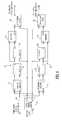
- FIG. 1diagrammatically illustrates the overall system configuration of a non-limiting, but preferred embodiment of the frequency shift keyed non-propagating magnetic field-based communication system of the present invention
- FIG. 2shows a first embodiment of a transmitter unit that may be employed in the system of FIG. 1;
- FIG. 3shows an alternative embodiment of a transmitter unit that may be employed in the system of FIG. 1;
- FIG. 4diagrammatically illustrates the receiver unit of the system of FIG. 1;
- FIG. 5diagrammatically illustrates the configuration of the digital receiver portion of the receiver of FIG. 4 .
- the inventionresides primarily in prescribed modular arrangements of conventional magnetic field generation and sensing components, in combination with digital communication circuits and associated digital signal processing components and attendant supervisory control circuitry therefor, that controls the operations of such circuits and components.
- these modular arrangementsmay be readily implemented using relatively compact analog field coils and associated capacitors, that are coupled with application specific integrated circuit (ASIC) chip sets, programmable digital signal processors, or general purpose processors.
- ASICapplication specific integrated circuit
- FIG. 1diagrammatically illustrates the overall system configuration of a non-limiting, but preferred embodiment of the frequency shift keyed non-propagating magnetic field-based communication system of the present invention, as comprising a transmitter unit 1 and a receiver unit 2 , which are linked together by means of a non-propagating magnetic field 3 generated and FSK-modulated by the transmitter unit 1 and detected and demodulated by the receiver unit 2 .
- the transmitter unit 1is operative to generate and FSK-modulate the non-propagating magnetic field 3 in accordance with modulation signals representative of digital data to be transmitted to the receiver unit.
- the transmitter unit 1comprises an analog section 10 , which is configured to generate and FSK-modulate the non-propagating magnetic field, and a digital section 20 that is operative to convert an incoming digital data stream (DATA_IN) supplied to a transmitter input port 21 into switch control signals.
- switch control signalsare used to controllably switch the resonant frequency of magnetic coil—capacitor components of the analog section between first and second precisely calibrated or pre-tuned frequency values, and thereby effect FSK-modulation of the magnetic field in accordance with the digital data.
- the analog sectionincludes a magnetic field coil 11 , relatively large amplitude energizing current for which is supplied by a DC power supply or battery 12 , that is coupled to the coil by way of a ‘pumping’ switch 13 .
- the magnetic field coil 11is small compared to the volumetric extent of its generated magnetic field, so that the energy in the magnetic field is not propagated, but is physically confined about the axis of the coil, as in a typical solenoid architecture.
- the pumping switch 13Under supervisory digital control of a zero-crossing detector 22 coupled in parallel with a resonant (‘tank’ or ‘ringing’) circuit 14 formed by the field coil 11 and one or more capacitors 15 - 0 - 15 -N, and 15 -FSK of a capacitor circuit 15 , the pumping switch 13 is periodically closed and opened in a fly-back manner, to provide a DC current boost to the coil 1 from the battery 12 , in order to compensate for resistive losses in the ringing circuit 14 .
- tankor ‘ringing’
- the pumping signal generated by the zero crossing detector 22provides for switch closure at or near the point at which the resonating current signal in the tank circuit crosses zero.
- This pumping signalhas a duration for a small fraction of a cycle of the resonant frequency of the magnetic field, and may be optimized for the intended range of operation of the generated field and the size of coil 11 .
- the zero crossing points of the resonant frequencyare supplied to a supervisory microcontroller 23 , for control of capacitor insertion switches of the capacitor circuit 15 and thereby FSK modulation of the resonant magnetic field.
- a first base frequency-defining capacitor 15 - 0is hardwired electrically in parallel with the coil 11 , while the remaining capacitors 15 -FSK and 15 - 1 - 15 -N are selectively connected in parallel with the coil 11 by the selective closure of respective series connected switches 16 -FSK and 16 - 1 - 16 -N.
- the switches 16may be implemented as digitally controllable electronic switch devices, such as, but not limited to field effect transistors (FETs), bipolar transistors, and the like.
- the selective closure of one or more of the switches 16 by the supervisory microcontroller 23places one or more of the capacitors 15 in parallel with the base capacitor 15 - 0 , so as to controllably lower or tune the resonant frequency of generated magnetic field.
- the microcontroller 23 of the digital section 20requires a clock signal as a modulation reference.
- a base frequency as defined by the coil 11 and the base capacitor 15 - 0 of the tank circuit 14may be employed; alternatively, a separate, independent clock source, such as a crystal oscillator 24 , may be used.
- the digital control section 20may also adjust the resonant frequency to account for tolerances due to component variation or proximity of ferrous metals to the field coil 11 .
- capacitors 15 - 1 , . . . , 15 -Nconstitute additional, small valued capacitors that may be selectively coupled in parallel with the base capacitor 15 - 0 and/or an FSK capacitor 15 -FSK by associated by-pass switches 16 - 1 , . . . , 16 -N, to provide for vernier tuning of the resonant frequency of the tank circuit 14 .
- the independent clock sourceacts as a reference for the supervisory microcontroller 23 to measure the resonant frequency established by the tank circuit 14 , at transmitter initialization and periodically thereafter.
- the vernier adjustment capacitors 15 - 1 , . . . , 15 -Nmay be controllably switched in and out of the resonator circuit 14 to determine the optimum frequency matches for the desired frequency pair. Thereafter, during data transmission, these ‘best match’ capacitors are switchably inserted in parallel with the base capacitor 15 - 0 and capacitor 15 -FSK, as necessary, to define the resonant frequencies associated with the binary states of the digital data.
- FIG. 3shows a reduced hardware complexity embodiment of the transmitter unit, where microcontroller 23 of the digital section generates and controls the pulse timing and duration used to pump the field coil 11 .
- the transmitter unit of FIG. 3eliminates some of the analog circuitry at the cost of requiring accurate, temperature-stable components in the resonant LC network. This embodiment is preferred in small battery-operated and portable applications.
- the analog portion 10 of the transmitter unit of FIG. 3places a relatively low inductance auxiliary coil 11 A in a transformer-coupled configuration with the high inductance field coil 11 .
- the auxiliary coil 11 Ais coupled to the battery 12 through the pumping switch 13 , selective closure of which is controlled directly by the microcontroller 23 . Because the field generating tank circuit is now DC-isolated from the pumping switch, a relatively simple switch can be used.
- Both transmitter embodimentswhen employed in heavy industrial applications, benefit from a power control loop.
- Thisallows for correction of the magnetic field level, thereby maintaining communication performance, when the system is affected by the proximity of metal such as a passing automobile or forklift.
- the power source 12may be appropriately adjusted by a control signal generated by monitoring the level of the voltage present in the resonant LC circuit.
- the power source 12may be controllably varied by means of an adjustable regulator 12 R, wherein the detected resonant circuit voltage is fed back via a feed back link 12 FB to the adjustment portion of the regulator 12 R, to form a closed control loop.
- the receiver unit of the system of FIG. 1is illustrated diagrammatically in FIG. 4 as comprising a resonant (LC tank) detector circuit 30 that includes a magnetic field-sensing coil 31 coupled in parallel with an associated capacitor 32 .
- the inductance-capacitance parameters of coil 31 and capacitor 32are such that the tank circuit 30 resonates at a frequency between the two FSK frequencies employed by the transmitter unit.
- the resonant frequency of the receiver tank circuit 30may be 121 kHz.
- the resonant detector circuit 30is coupled to a sense amplifier 35 , which amplifies the voltage produced by the receiver detector circuit for the desired receiver sensitivity and buffers the detected voltage to the appropriate logic level for use by a digital receiver 40 , the output of which is coupled to a state machine-based demodulator 45 .
- the digital receiver 40is referenced to a prescribed receiver clock frequency F RCLK , as may be supplied by a crystal clock 42 .
- the receiver clockis set to a frequency corresponding to the difference between the FSK frequencies of the selected modulation pair.
- the use of such a relatively low clock frequency in the receiverrequires a slower data rate, since one clock cycle of the receiver clock represents only 3.4-3.8 FSK clock cycles.
- the digital receivercontains two signal buffer paths 50 and 60 , that operate on alternate sample periods that are one-half the period of the received data spread code. This ensures that at least one of the two buffer paths will not be sampling data during transitions in the received FSK frequency.
- the data spreading codemay comprise a Manchester (two-chip spreading) or other relatively short spreading code used for reduced complexity data communications.
- the output of the receiver unit's sense amplifier 35is coupled over line 36 to clock inputs of each of a frequency counter 51 and 61 , the contents of which are coupled to data (D) inputs of sample shift registers or A latches 52 and 62 , that are respectively coupled in cascade with associated B latches 53 and 54 .
- the contents of the frequency counters 51 and 61are cleared or reset to zero, upon an active reset being applied from prescribed bit stages of a latch control counter 70 to their respective clear inputs CLR from prescribed bit stages.
- latch control counter 70may comprise an eight bit counter. As long as they are enabled, the contents of frequency counters 51 and 61 are modified (e.g., incremented) by the rising edge of the change in the output signal from sense amplifier 35 .
- the contents of the frequency counters 51 and 61are respectively transferred or clocked into their associated A latches 52 and 62 ; also, the current contents of the A latches 52 and 62 are clocked into the cascaded B latch 53 and 63 , respectively.
- a latches 52 and 62Since the contents of A latches 52 and 62 indicate the number of successive rising edges of the received signal within a prescribed measurement interval (sample time), they are representative of the frequency of the latched data. These count values are coupled to respective A inputs of subtraction units 54 and 64 , whose B inputs are coupled to the outputs of latches 53 and 63 .
- the difference outputs DIFF provided by subtraction units 54 and 64are coupled to the D inputs of respective difference latches 55 and 65 .
- the difference latches 55 and 65whose contents are coupled to a state machine within the demodulator 45 , are clocked by the latch control counter 70 , as described above.
- the contents of frequency counters 51 and 61are loaded into the A latches 52 and 62 , and the contents of the A latches 52 and 62 , respectively are transferred to B latches 53 and 63 , for comparison with the next tone (frequency) clocked into the A latches 52 and 62 .
- the difference latches 55 and 65are clocked.
- the differences between the contents of latches 52 and 53 , and between the contents of latches 62 and 63 , as output by subtraction units 54 and 64are coupled to the state machine, which demodulates the spreading code of the data.
- the demodulated datais then buffered, so that it may be clocked out for validation of parameters such as preamble, cyclic redundancy check (CRC) code sequence and message length.
- CRCcyclic redundancy check
- the state machinecompares a received sequence of FSK tones with a predefined start-of-message sequence (corresponding to a start synchronization code) .
- the start-of-message sequencemay comprise a plurality of successive samples at one FSK frequency or tone (such as three spreading chip periods at the higher of the two FSK tones), followed by a plurality of successive samples at the second FSK frequency (e.g., three spreading chip periods at the lower of the two FSK tones).
- the difference between the contents of the respective A and B latches 52 / 62 and 53 / 63would be the numerical sequence (0, 0, ⁇ N, 0, 0).
- the state machineUpon detecting this sequence, the state machine initializes the data demodulation circuitry, so that the data may be clocked out as it is detected and demodulated.
- data values of ‘1’ and ‘0’are represented by respectively difference sequences of the two FSK tones.
- a logical ‘one’may correspond to one spreading chip period at the higher FSK tone (147.5 KhZ) followed by one spreading chip period at the lower FSK tone (114.7 kHz);
- a logical ‘zero’may correspond to one spreading chip period at the lower FSK tone (114.7 kHz), followed by one spreading chip period at the higher FSK tone (147.5 KhZ).
- the data bit sequence (00)would result in latch differences of ( ⁇ N,+N); the data bit sequence (01) would result in latch differences of (0,+N); the data bit sequence (10) would result in latch differences of (0, ⁇ N); and the data bit sequence (11) would result in latch differences of (+N, ⁇ N).
- Thisallows a determination of the logic level provided at the output at the end of each sample period to be clocked out. It also provides for detection of any errors in format that may indicate corruption of the data.
- the state machinemay detect the end of a message by comparing a received sequence of FSK tones with a predefined end-of-message sequence.
- the end-of-message sequencemay be complementary to the start-of-message sequence, described above. Namely, in the present example, an and-of-message sequence may comprise a three spreading chip periods at the lower of the two FSK tones), followed by three spreading chip periods at the higher of the two FSK tones) . In this case, the difference between the contents of the A and B latches would be the numerical sequence (0, 0, +N, 0, 0).
- the state machineUpon detecting a valid end-of message sequence, the state machine returns the receiver's demodulation circuitry to its idle state.
- the present inventionprovides a relatively compact, and reduced complexity communication system that FSK-modulates a non-propagating magnetic field for simplex digital communications, without restriction to the amount of data transmitted between a modulating source and an associated demodulating receiver.
- Thismakes the invention readily suited for real time location systems for locating and/or identifying transponder-tagged objects.
Landscapes
- Physics & Mathematics (AREA)
- Life Sciences & Earth Sciences (AREA)
- General Life Sciences & Earth Sciences (AREA)
- General Physics & Mathematics (AREA)
- Geophysics (AREA)
- Digital Transmission Methods That Use Modulated Carrier Waves (AREA)
Abstract
Description
Claims (16)
Priority Applications (5)
| Application Number | Priority Date | Filing Date | Title |
|---|---|---|---|
| US09/689,340US6349116B1 (en) | 1999-10-14 | 2000-10-12 | Data communication system harnessing frequency shift keyed magnetic field |
| US09/759,290US6853687B2 (en) | 2000-01-12 | 2001-01-11 | Proximity-based magnetic field generator for controlling operation of RF burst-transmitting tags of geolocation system |
| US09/818,276US6812839B1 (en) | 2000-03-27 | 2001-03-27 | Use of rotating magnetic field to enhance communication with RF burst-transmitting tags of object location system |
| AU2001251022AAU2001251022A1 (en) | 2000-03-27 | 2001-03-27 | Use of rotating magnetic field to enhance communication with rf burst-transmitting tags of object location system |
| PCT/US2001/009781WO2001074020A1 (en) | 2000-03-27 | 2001-03-27 | Use of rotating magnetic field to enhance communication with rf burst-transmitting tags of object location system |
Applications Claiming Priority (2)
| Application Number | Priority Date | Filing Date | Title |
|---|---|---|---|
| US15965899P | 1999-10-14 | 1999-10-14 | |
| US09/689,340US6349116B1 (en) | 1999-10-14 | 2000-10-12 | Data communication system harnessing frequency shift keyed magnetic field |
Related Child Applications (2)
| Application Number | Title | Priority Date | Filing Date |
|---|---|---|---|
| US09/759,290Continuation-In-PartUS6853687B2 (en) | 2000-01-12 | 2001-01-11 | Proximity-based magnetic field generator for controlling operation of RF burst-transmitting tags of geolocation system |
| US09/818,276Continuation-In-PartUS6812839B1 (en) | 2000-03-27 | 2001-03-27 | Use of rotating magnetic field to enhance communication with RF burst-transmitting tags of object location system |
Publications (1)
| Publication Number | Publication Date |
|---|---|
| US6349116B1true US6349116B1 (en) | 2002-02-19 |
Family
ID=26856159
Family Applications (1)
| Application Number | Title | Priority Date | Filing Date |
|---|---|---|---|
| US09/689,340Expired - LifetimeUS6349116B1 (en) | 1999-10-14 | 2000-10-12 | Data communication system harnessing frequency shift keyed magnetic field |
Country Status (1)
| Country | Link |
|---|---|
| US (1) | US6349116B1 (en) |
Cited By (15)
| Publication number | Priority date | Publication date | Assignee | Title |
|---|---|---|---|---|
| US20040080316A1 (en)* | 2001-11-20 | 2004-04-29 | Friend Timothy R. | Magnetometer having a dynamically adjustable bias setting and electronic vehicle compass incorporating the same |
| US20060084380A1 (en)* | 2004-11-04 | 2006-04-20 | Hoyt Reed W | Systems and methods for short range wireless communication |
| US20060192628A1 (en)* | 2002-06-20 | 2006-08-31 | Alfred E. Mann Foundation For Scientific Research | System and method for automatic tuning of a magnetic field generator |
| US20070013540A1 (en)* | 2005-07-14 | 2007-01-18 | Altmann Andres C | Wireless position transducer with digital signaling |
| US20070100517A1 (en)* | 2003-07-02 | 2007-05-03 | Bong-Taek Kim | Atps for controlling train using data communication |
| US20070248180A1 (en)* | 2006-04-19 | 2007-10-25 | Wherenet Corp., Corporation Of The State Of California | Receiver for object locating and tracking systems and related methods |
| US20080186115A1 (en)* | 2007-02-05 | 2008-08-07 | Sony Corporation | Method for adjusing tuning circuit and receiver circuit |
| WO2009012009A1 (en)* | 2007-07-16 | 2009-01-22 | Boston Scientific Neuromodulation Corporation | Energy efficient resonant driving circuit for magnetically coupled telemetry |
| US20090201169A1 (en)* | 2008-02-07 | 2009-08-13 | Mark Iv Industries Corp. | Real-Time Location Systems and Methods |
| US20110042340A1 (en)* | 2003-03-06 | 2011-02-24 | De Carvalho David | Air Vent for Liquid Containers, Based on the Principle of Communicating Vessels |
| US8078103B2 (en) | 2005-10-31 | 2011-12-13 | Zih Corp. | Multi-element RFID coupler |
| US20120139358A1 (en)* | 2010-12-01 | 2012-06-07 | Triune Ip Llc | Multiple Coil Data Transmission System |
| US8334801B2 (en) | 2010-07-26 | 2012-12-18 | Ensco, Inc. | System and method for real-time locating |
| US10193720B1 (en)* | 2017-09-29 | 2019-01-29 | The United States Of America, As Represented By The Secretary Of The Army | Chaotically modulated communications with switched-capacitance resistance tuning |
| CN113411095A (en)* | 2021-06-30 | 2021-09-17 | 杭州电子科技大学 | Induction coil signal receiving circuit based on numerical control resonant frequency |
Citations (8)
| Publication number | Priority date | Publication date | Assignee | Title |
|---|---|---|---|---|
| USRE32627E (en) | 1981-09-10 | 1988-03-22 | Sensormatic Electronics Corporation | Electrical surveillance apparatus with moveable antenna elements |
| US5103459A (en) | 1990-06-25 | 1992-04-07 | Qualcomm Incorporated | System and method for generating signal waveforms in a cdma cellular telephone system |
| US5432841A (en) | 1992-07-10 | 1995-07-11 | Rimer; Neil A. | System for locating and communicating with mobile vehicles |
| US5437057A (en)* | 1992-12-03 | 1995-07-25 | Xerox Corporation | Wireless communications using near field coupling |
| US5481588A (en) | 1993-04-06 | 1996-01-02 | Alcatel N.V. | Test arrangements for radio telephone systems |
| US5485632A (en) | 1993-02-26 | 1996-01-16 | Motorola, Inc. | Method for initiating and determining simulcast transmission of a message |
| US5561701A (en) | 1992-01-10 | 1996-10-01 | Nec Corporation | Radio paging system having a plurality of transmitter stations |
| US5644108A (en) | 1994-07-18 | 1997-07-01 | Wacom Co., Ltd. | Position detection device utilizing electromagnetic induction |
- 2000
- 2000-10-12USUS09/689,340patent/US6349116B1/ennot_activeExpired - Lifetime
Patent Citations (9)
| Publication number | Priority date | Publication date | Assignee | Title |
|---|---|---|---|---|
| USRE32627E (en) | 1981-09-10 | 1988-03-22 | Sensormatic Electronics Corporation | Electrical surveillance apparatus with moveable antenna elements |
| US5103459A (en) | 1990-06-25 | 1992-04-07 | Qualcomm Incorporated | System and method for generating signal waveforms in a cdma cellular telephone system |
| US5103459B1 (en) | 1990-06-25 | 1999-07-06 | Qualcomm Inc | System and method for generating signal waveforms in a cdma cellular telephone system |
| US5561701A (en) | 1992-01-10 | 1996-10-01 | Nec Corporation | Radio paging system having a plurality of transmitter stations |
| US5432841A (en) | 1992-07-10 | 1995-07-11 | Rimer; Neil A. | System for locating and communicating with mobile vehicles |
| US5437057A (en)* | 1992-12-03 | 1995-07-25 | Xerox Corporation | Wireless communications using near field coupling |
| US5485632A (en) | 1993-02-26 | 1996-01-16 | Motorola, Inc. | Method for initiating and determining simulcast transmission of a message |
| US5481588A (en) | 1993-04-06 | 1996-01-02 | Alcatel N.V. | Test arrangements for radio telephone systems |
| US5644108A (en) | 1994-07-18 | 1997-07-01 | Wacom Co., Ltd. | Position detection device utilizing electromagnetic induction |
Cited By (35)
| Publication number | Priority date | Publication date | Assignee | Title |
|---|---|---|---|---|
| US7053608B2 (en)* | 2001-11-20 | 2006-05-30 | Gentex Corporation | Magnetometer having a dynamically adjustable bias setting and electronic vehicle compass incorporating the same |
| US20040080316A1 (en)* | 2001-11-20 | 2004-04-29 | Friend Timothy R. | Magnetometer having a dynamically adjustable bias setting and electronic vehicle compass incorporating the same |
| US20060192628A1 (en)* | 2002-06-20 | 2006-08-31 | Alfred E. Mann Foundation For Scientific Research | System and method for automatic tuning of a magnetic field generator |
| US7515012B2 (en)* | 2002-06-20 | 2009-04-07 | Alfred E. Mann Foundation For Scientific Research | System and method for automatic tuning of a magnetic field generator |
| US20110042340A1 (en)* | 2003-03-06 | 2011-02-24 | De Carvalho David | Air Vent for Liquid Containers, Based on the Principle of Communicating Vessels |
| US8196785B2 (en) | 2003-03-06 | 2012-06-12 | De Carvalho David | Air vent for liquid containers, based on the principle of communicating vessels |
| US20070100517A1 (en)* | 2003-07-02 | 2007-05-03 | Bong-Taek Kim | Atps for controlling train using data communication |
| US20060084380A1 (en)* | 2004-11-04 | 2006-04-20 | Hoyt Reed W | Systems and methods for short range wireless communication |
| US7933554B2 (en)* | 2004-11-04 | 2011-04-26 | The United States Of America As Represented By The Secretary Of The Army | Systems and methods for short range wireless communication |
| US20070013540A1 (en)* | 2005-07-14 | 2007-01-18 | Altmann Andres C | Wireless position transducer with digital signaling |
| EP3379298A1 (en)* | 2005-07-14 | 2018-09-26 | Biosense Webster, Inc. | Wireless position transducer with digital signaling |
| EP3376263A1 (en)* | 2005-07-14 | 2018-09-19 | Biosense Webster, Inc. | Wireless position transducer with digital signaling |
| US8730011B2 (en) | 2005-07-14 | 2014-05-20 | Biosense Webster, Inc. | Wireless position transducer with digital signaling |
| CN1911171B (en)* | 2005-07-14 | 2012-10-03 | 韦伯斯特生物官能公司 | Wireless position transducer with digital signalling |
| EP1744184A3 (en)* | 2005-07-14 | 2009-07-15 | Biosense Webster, Inc. | Wireless position transducer with digital signaling |
| US8306474B2 (en) | 2005-10-31 | 2012-11-06 | Zih Corp. | Multi-element RFID coupler |
| US8078103B2 (en) | 2005-10-31 | 2011-12-13 | Zih Corp. | Multi-element RFID coupler |
| US9391675B2 (en) | 2005-10-31 | 2016-07-12 | Zih Corp. | Multi-element RFID coupler |
| US20070248180A1 (en)* | 2006-04-19 | 2007-10-25 | Wherenet Corp., Corporation Of The State Of California | Receiver for object locating and tracking systems and related methods |
| WO2007123812A1 (en)* | 2006-04-19 | 2007-11-01 | Wherenet Corp | Receiver for object locating and tracking systems and related methods |
| GB2452640A (en)* | 2006-04-19 | 2009-03-11 | Wherenet Corp | Receiver for object locating and tracking systems and related methods |
| US8265191B2 (en) | 2006-04-19 | 2012-09-11 | Zebra Enterprise Solutions Corp. | Receiver for object locating and tracking systems and related methods |
| GB2452640B (en)* | 2006-04-19 | 2010-12-08 | Wherenet Corp | Receiver for object locating and tracking systems and related methods |
| US20080186115A1 (en)* | 2007-02-05 | 2008-08-07 | Sony Corporation | Method for adjusing tuning circuit and receiver circuit |
| US7979040B2 (en)* | 2007-02-05 | 2011-07-12 | Sony Corporation | Method for adjusting tuning circuit and receiver circuit |
| WO2009012009A1 (en)* | 2007-07-16 | 2009-01-22 | Boston Scientific Neuromodulation Corporation | Energy efficient resonant driving circuit for magnetically coupled telemetry |
| US9162068B2 (en) | 2007-07-16 | 2015-10-20 | Boston Scientific Neuromodulation Corporation | Energy efficient resonant driving circuit for magnetically coupled telemetry |
| US20090024179A1 (en)* | 2007-07-16 | 2009-01-22 | Advanced Bionics Corporation | Energy efficient resonant driving circuit for magnetically coupled telemetry |
| US9403021B2 (en) | 2007-07-16 | 2016-08-02 | Boston Scientific Neuromdulation Corporation | Energy efficient resonant driving circuit for magnetically coupled interaction with an implantable medical device |
| US20090201169A1 (en)* | 2008-02-07 | 2009-08-13 | Mark Iv Industries Corp. | Real-Time Location Systems and Methods |
| US8334801B2 (en) | 2010-07-26 | 2012-12-18 | Ensco, Inc. | System and method for real-time locating |
| US10079090B2 (en)* | 2010-12-01 | 2018-09-18 | Triune Systems, LLC | Multiple coil data transmission system |
| US20120139358A1 (en)* | 2010-12-01 | 2012-06-07 | Triune Ip Llc | Multiple Coil Data Transmission System |
| US10193720B1 (en)* | 2017-09-29 | 2019-01-29 | The United States Of America, As Represented By The Secretary Of The Army | Chaotically modulated communications with switched-capacitance resistance tuning |
| CN113411095A (en)* | 2021-06-30 | 2021-09-17 | 杭州电子科技大学 | Induction coil signal receiving circuit based on numerical control resonant frequency |
Similar Documents
| Publication | Publication Date | Title |
|---|---|---|
| US6349116B1 (en) | Data communication system harnessing frequency shift keyed magnetic field | |
| JP3841826B2 (en) | Micropower RF transponder | |
| US6853687B2 (en) | Proximity-based magnetic field generator for controlling operation of RF burst-transmitting tags of geolocation system | |
| US6703921B1 (en) | Operation in very close coupling of an electromagnetic transponder system | |
| US6434194B1 (en) | Combined OOK-FSK/PPM modulation and communication protocol scheme providing low cost, low power consumption short range radio link | |
| US4818855A (en) | Identification system | |
| US6980657B1 (en) | Communications system using chaotic synchronized circuits | |
| JP3649081B2 (en) | Electromagnetic transponder reading terminal operating in very close coupling | |
| US4796028A (en) | Apparatus for bidirectional data transmission | |
| NL1001761C2 (en) | System for contactless data exchange between a reading and writing unit and one or more information carriers. | |
| HU182543B (en) | Sensing board of passive circuit for identification devices | |
| CA2557961C (en) | Method for detecting identification media | |
| US20100142665A1 (en) | Methods of Processing A Wireless Communication Signal, Wireless Communication Synchronization Methods, and A Radio Frequency Ideentification Device Communication Method | |
| JP3829577B2 (en) | Full duplex transmission method of electromagnetic transponder system | |
| US20010025887A1 (en) | Portable electronic apparatus, IC card and reader/writer | |
| HU216494B (en) | Electronic locking mechanism | |
| EP0823059A1 (en) | Interrogator for electronic identification system | |
| US6185264B1 (en) | Apparatus and method for frequency shift keying | |
| WO2003009482A1 (en) | Superregenerative low-power receiver | |
| CZ2007527A3 (en) | Device for reading contactless integrated circuits | |
| CN110521127A (en) | The adaptively sampled demodulation of the peak value of RF transceiver | |
| JP2000307465A (en) | Bpsk demodulating circuit and noncontact ic card system with the circuit | |
| JPH04293320A (en) | Transmission circuit for contactless medium communication with resonance circuit | |
| JPH07123120A (en) | Data transmission / reception system | |
| JP3629342B2 (en) | Object identification device |
Legal Events
| Date | Code | Title | Description |
|---|---|---|---|
| STCF | Information on status: patent grant | Free format text:PATENTED CASE | |
| AS | Assignment | Owner name:SILICON VALLEY BANK, CALIFORNIA Free format text:SECURITY AGREEMENT;ASSIGNOR:WHERENET CORP.;REEL/FRAME:014918/0646 Effective date:20030428 | |
| FEPP | Fee payment procedure | Free format text:PAT HOLDER CLAIMS SMALL ENTITY STATUS, ENTITY STATUS SET TO SMALL (ORIGINAL EVENT CODE: LTOS); ENTITY STATUS OF PATENT OWNER: LARGE ENTITY | |
| REFU | Refund | Free format text:REFUND - PAYMENT OF MAINTENANCE FEE, 4TH YEAR, LARGE ENTITY (ORIGINAL EVENT CODE: R1551); ENTITY STATUS OF PATENT OWNER: LARGE ENTITY | |
| FPAY | Fee payment | Year of fee payment:4 | |
| AS | Assignment | Owner name:WHERENET CORPORATION, CALIFORNIA Free format text:RELEASE BY SECURED PARTY;ASSIGNOR:SILICON VALLEY BANK;REEL/FRAME:018866/0148 Effective date:20070129 | |
| AS | Assignment | Owner name:SILICON VALLEY BANK, CALIFORNIA Free format text:SECURITY INTERESTS RELEASE;ASSIGNOR:WHERENET CORP.;REEL/FRAME:018855/0734 Effective date:20070125 | |
| FEPP | Fee payment procedure | Free format text:PAYOR NUMBER ASSIGNED (ORIGINAL EVENT CODE: ASPN); ENTITY STATUS OF PATENT OWNER: LARGE ENTITY | |
| FEPP | Fee payment procedure | Free format text:PAT HOLDER NO LONGER CLAIMS SMALL ENTITY STATUS, ENTITY STATUS SET TO UNDISCOUNTED (ORIGINAL EVENT CODE: STOL); ENTITY STATUS OF PATENT OWNER: LARGE ENTITY | |
| REFU | Refund | Free format text:REFUND - PAYMENT OF MAINTENANCE FEE, 8TH YR, SMALL ENTITY (ORIGINAL EVENT CODE: R2552); ENTITY STATUS OF PATENT OWNER: LARGE ENTITY | |
| FPAY | Fee payment | Year of fee payment:8 | |
| AS | Assignment | Owner name:ZEBRA ENTERPRISE SOLUTIONS CORP., CALIFORNIA Free format text:CHANGE OF NAME;ASSIGNOR:WHERENET CORP.;REEL/FRAME:025217/0323 Effective date:20090713 | |
| FPAY | Fee payment | Year of fee payment:12 | |
| AS | Assignment | Owner name:WHERENET CORP., CALIFORNIA Free format text:ASSIGNMENT OF ASSIGNORS INTEREST;ASSIGNORS:HASH, RONALD J.;BOWMAN, DOUGLAS C.;SIGNING DATES FROM 19991029 TO 19991101;REEL/FRAME:033691/0266 | |
| AS | Assignment | Owner name:MORGAN STANLEY SENIOR FUNDING, INC. AS THE COLLATERAL AGENT, MARYLAND Free format text:SECURITY AGREEMENT;ASSIGNORS:ZIH CORP.;LASER BAND, LLC;ZEBRA ENTERPRISE SOLUTIONS CORP.;AND OTHERS;REEL/FRAME:034114/0270 Effective date:20141027 Owner name:MORGAN STANLEY SENIOR FUNDING, INC. AS THE COLLATE Free format text:SECURITY AGREEMENT;ASSIGNORS:ZIH CORP.;LASER BAND, LLC;ZEBRA ENTERPRISE SOLUTIONS CORP.;AND OTHERS;REEL/FRAME:034114/0270 Effective date:20141027 | |
| AS | Assignment | Owner name:ZIH CORP., ILLINOIS Free format text:ASSIGNMENT OF ASSIGNORS INTEREST;ASSIGNOR:ZEBRA ENTERPRISE SOLUTIONS CORP.;REEL/FRAME:036503/0630 Effective date:20150828 | |
| AS | Assignment | Owner name:ZIH CORP., ILLINOIS Free format text:ASSIGNMENT OF ASSIGNORS INTEREST;ASSIGNOR:ZEBRA ENTERPRISE SOLUTIONS CORP.;REEL/FRAME:036552/0588 Effective date:20150828 | |
| AS | Assignment | Owner name:JPMORGAN CHASE BANK, N.A., AS THE SUCCESSOR AGENT, NEW YORK Free format text:PATENT SECURITY INTEREST ASSIGNMENT AGREEMENT;ASSIGNOR:MORGAN STANLEY SENIOR FUNDING, INC., AS THE EXISTING AGENT;REEL/FRAME:044791/0842 Effective date:20170907 Owner name:JPMORGAN CHASE BANK, N.A., AS THE SUCCESSOR AGENT, Free format text:PATENT SECURITY INTEREST ASSIGNMENT AGREEMENT;ASSIGNOR:MORGAN STANLEY SENIOR FUNDING, INC., AS THE EXISTING AGENT;REEL/FRAME:044791/0842 Effective date:20170907 | |
| AS | Assignment | Owner name:ZEBRA TECHNOLOGIES CORPORATION, ILLINOIS Free format text:MERGER;ASSIGNOR:ZIH CORP.;REEL/FRAME:048884/0618 Effective date:20181220 | |
| AS | Assignment | Owner name:JPMORGAN CHASE BANK, N.A., AS COLLATERAL AGENT, NE Free format text:NOTICE OF TRANSFER OF SECURITY INTEREST IN PATENTS;ASSIGNOR:ZEBRA TECHNOLOGIES CORPORATION;REEL/FRAME:049675/0049 Effective date:20190701 Owner name:JPMORGAN CHASE BANK, N.A., AS COLLATERAL AGENT, NEW YORK Free format text:NOTICE OF TRANSFER OF SECURITY INTEREST IN PATENTS;ASSIGNOR:ZEBRA TECHNOLOGIES CORPORATION;REEL/FRAME:049675/0049 Effective date:20190701 | |
| AS | Assignment | Owner name:JPMORGAN CHASE BANK, N.A., NEW YORK Free format text:SECURITY INTEREST;ASSIGNORS:ZEBRA TECHNOLOGIES CORPORATION;LASER BAND, LLC;TEMPTIME CORPORATION;REEL/FRAME:053841/0212 Effective date:20200901 | |
| AS | Assignment | Owner name:LASER BAND, LLC, ILLINOIS Free format text:RELEASE OF SECURITY INTEREST - 364 - DAY;ASSIGNOR:JPMORGAN CHASE BANK, N.A.;REEL/FRAME:056036/0590 Effective date:20210225 Owner name:ZEBRA TECHNOLOGIES CORPORATION, ILLINOIS Free format text:RELEASE OF SECURITY INTEREST - 364 - DAY;ASSIGNOR:JPMORGAN CHASE BANK, N.A.;REEL/FRAME:056036/0590 Effective date:20210225 Owner name:TEMPTIME CORPORATION, NEW JERSEY Free format text:RELEASE OF SECURITY INTEREST - 364 - DAY;ASSIGNOR:JPMORGAN CHASE BANK, N.A.;REEL/FRAME:056036/0590 Effective date:20210225 |