US6349061B1 - Non-volatile semiconductor memory - Google Patents
Non-volatile semiconductor memoryDownload PDFInfo
- Publication number
- US6349061B1 US6349061B1US09/375,697US37569799AUS6349061B1US 6349061 B1US6349061 B1US 6349061B1US 37569799 AUS37569799 AUS 37569799AUS 6349061 B1US6349061 B1US 6349061B1
- Authority
- US
- United States
- Prior art keywords
- semiconductor memory
- volatile semiconductor
- constant current
- regions
- sectors
- Prior art date
- Legal status (The legal status is an assumption and is not a legal conclusion. Google has not performed a legal analysis and makes no representation as to the accuracy of the status listed.)
- Expired - Lifetime
Links
Images

Classifications
- G—PHYSICS
- G11—INFORMATION STORAGE
- G11C—STATIC STORES
- G11C16/00—Erasable programmable read-only memories
- G11C16/02—Erasable programmable read-only memories electrically programmable
- G—PHYSICS
- G11—INFORMATION STORAGE
- G11C—STATIC STORES
- G11C16/00—Erasable programmable read-only memories
- G11C16/02—Erasable programmable read-only memories electrically programmable
- G11C16/06—Auxiliary circuits, e.g. for writing into memory
- G11C16/10—Programming or data input circuits
- G11C16/14—Circuits for erasing electrically, e.g. erase voltage switching circuits
- G11C16/16—Circuits for erasing electrically, e.g. erase voltage switching circuits for erasing blocks, e.g. arrays, words, groups
- G—PHYSICS
- G11—INFORMATION STORAGE
- G11C—STATIC STORES
- G11C16/00—Erasable programmable read-only memories
- G11C16/02—Erasable programmable read-only memories electrically programmable
- G11C16/04—Erasable programmable read-only memories electrically programmable using variable threshold transistors, e.g. FAMOS
- G11C16/0408—Erasable programmable read-only memories electrically programmable using variable threshold transistors, e.g. FAMOS comprising cells containing floating gate transistors
- G11C16/0425—Erasable programmable read-only memories electrically programmable using variable threshold transistors, e.g. FAMOS comprising cells containing floating gate transistors comprising cells containing a merged floating gate and select transistor
Definitions
- the present inventionrelates to a non-volatile semiconductor memory, and more particularly to a non-volatile semiconductor memory, such as an EPROM (Erasable and Programmable ROM), or EEPROM (referred to as Electrical Erasable and Programmable ROM, flash EEPROM, or flash memory), in which data are stored (written/read) by accumulating charges in a floating gate and detecting a change in a threshold voltage in terms of the presence or absence of the charges by a control gate.
- EPROMErasable and Programmable ROM
- EEPROMElectrical Erasable and Programmable ROM
- flash EEPROMflash memory
- a technique of using a redundant memory cell built in a semiconductor memory in place of a memory cell which cannot be used because of its defecthas been developed.
- the address of a defective memory cellcan be known in the process of manufacturing the semiconductor memory.
- the address of the defective memory cellis stored previously in a redundant address. It is always observed whether or not the address generated from a normal address generating circuit is that of the defective cell. If so, the redundant memory cell is addressed in place of the defective memory cell. Namely, the address line having the defective memory cell is not used.
- FIG. 3is a circuit showing a part of an addressing circuit 1 of the semiconductor memory having such a redundancy function.
- An address data for addressingis applied to the address generating circuit 1 .
- An address data of a defective memory cellwhich can be known from a test during the manufacturing process of the semiconductor memory cell, is applied to a redundant address generating circuit 2 .
- a comparator 3compares an output signal from the address generating circuit and that from the redundant address generating circuit 1 . In this case, it generates a “H” level signal when the address data of the defective memory cell is generated from the address generating circuit 1 , and an “L” level signal in other cases.
- a first switching meansdetermines whether or not the output signal from the address generating circuit 1 should be selected according to the output from the comparator 3 .
- Each of decodersdecodes the address data from the first switching means 4 .
- the decodingintends to designate the normal memory cell, or to designate the defective memory cell, i.e. to decode the address for redundancy.
- These decoders 5 A, 5 B, 5 C and 5 Dare connected to word lines WL 0 , WL 1 , WL 2 and WL 3 , respectively. Although not shown, a larger number of decoders and WL's are actually connected.
- the output signal from the address generating circuit 1is applied to the decoders 5 A, 5 B, 5 C and 5 D through the first switching means 4 .
- the output from the decoder corresponding to the selected WLbecomes “L” level.
- the memory cellis designated.
- the “H” levelis generated from the comparator 3 so that the “L” level is applied to each of the AND gates constituting the first switching means 4 .
- the address from the address generating circuit 1is not applied to the decoders 5 A, 5 B, 5 C and 5 D.
- the “H” level from the comparator 3is applied to an AND gate 6 so as to be conductive.
- the addressing signal from the redundant address generating circuit 2is sent to a redundant word line RWL through the AND gate 6 so that the redundant memory cell can be addressed.
- the redundant addresscan be designated.
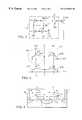
- non-volatile semiconductor memory cellis roughly classified into a split-gate type and a stacked-gate type
- split-gate type non-volatile semiconductor memoryas disclosed in WO92/18980 (G11C13/00) will be explained.
- FIG. 4is a circuit diagram of a memory cell array 21 in which non-volatile memories 20 A, 20 B, 20 C and 20 D are arranged in a matrix form.
- FIG. 5is a view showing the structure of a certain memory cell therein.
- non-volatile semiconductor memories 20 A and 20 B, and 20 C and 20 Dtheir source regions are commonly connected to a source line SL, and their drain regions are connected to bit lines BL 0 , and BL 1 , respectively.
- the control gates CG's of the non-volatile memories 20 A and 20 C, and 20 B and 20 Dare connected to word lines WL 0 and WL 1 , respectively.
- FIG. 5since the control gate electrode CG is formed from on the upper surface of the floating gate electrode to on the side surface thereof, a distance between the control gate electrode CG and the bit lines becomes narrower.
- the interval between the bit lines BL 0 , BL 1 and control gates CG's (word lines)becomes very narrow so that short-circuiting is likely to occur in comparison with the stacked gate structure in which control gate electrode is formed on the floating gate electrode.
- the memory at issuecannot be used and dealt with as a defective cell
- the writing operationis made as follows.
- the voltages of e.g. 0 V, 11V and 2Vare applied to the bit line BL 0 , source line SL and word line WL 0 , respectively.
- the potential of a floating gate FG which is strongly capacitive-coupled with a diffused layer (not shown) constituting the source lineis raised to about 9 V.
- hot electrons generated between the drain region and source regionjump into the floating gate FG, thus making the data writing operation.
- the reading operationis made as follows.
- the voltages of e.g. 2 V, 0 V and 4 Vare applied to the bit line BL 0 , source line SL and word line WL 0 , respectively.
- the erasureis made as follows.
- the voltages of e.g. 0 V, 0 V and 14 Vare applied to the bit line BL 0 , source line SL and word line WL 0 , respectively. Then, the charge stored in the floating gate is pulled out toward the control gate CG so that the data is erased.
- all the decoders 5 A, 5 B, 5 C and 5 Dare selected for data erasure.
- the high voltage from the high voltage generating circuit 8is applied to the word lines WL 0 , WL 1 , WL 2 and WL 3 through the decoders 5 A, 5 B, 5 C and 5 D, respectively. If there is leakage failure in any memory cell (cell directed to redundancy) connected to the word lines WL 0 , WL 1 , WL 2 and WL 3 , the voltage on these word lines cannot be raised to about 14 V. Therefore, erasure cannot be normally made for all the memory cells connected to WL 0 , WL 1 , WL 2 and WL 3 .
- the leakage failurerefers to short-circuiting in the word line WL's that is a phenomenon that excessive current flows through the word line WL. This is attributable to that poor connecting occurs between the word line WL and bit line BL.
- the storage areais divided into a plurality of regions called sectors.
- One sectoris a minimum unit for which collective erasure can be made. Using the sector facilitates local erasure.
- the entire chipmay include the sector having the cell suffering from the above leakage failure (although the poor sector is replaced by the redundant sector, it is included for the object for erasure when collective erasure is made for the entire chip). If the chip includes such a sector, as described above, the high voltage required for erasure cannot be supplied to each control gate. Namely, the faulty sector which is an object for redundancy will affect the normal sector.
- the present inventionintends to provide a non-volatile semiconductor memory for which collective erasure can be made irrespectively of whether or not there is any faulty sector which is an object of redundancy.
- a first aspect of the memoryis a non-volatile semiconductor memory having a plurality of regions of sectors collectively erasable of stored data of the present invention, which comprises: a high voltage generating circuit for generating a high voltage used for erasing data for the non-volatile semiconductor memory; and a plurality of constant current circuits each connected between said high voltage generating circuit and said plurality of sector regions; wherein said plurality of constant current circuits are operated in collective erasure of the data so as to limit the current flowing through said plurality of regions of sectors.
- a second aspect of the present inventionis a non-volatile semiconductor memory according to the first aspect, wherein each of said plurality of constant current circuits is a current mirror circuit, and constant current transistors each of which produces an output current corresponding to an input current to said current mirror circuit are connected to said plurality of regions of sectors.
- a third aspect of the present inventionis a non-volatile semiconductor memory according to the first aspect, which further comprises a switch for releasing the constant current operation by said plurality of transistors during non-erasure operation of the data.
- a fourth aspect of the present inventionis a non-volatile semiconductor memory according to the first aspect, wherein said non-volatile semiconductor memory is a split-gate type of EEPROM, and each of said current mirror circuits is connected each of word lines of said EEPROM.
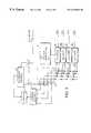
- a non-volatile semiconductor memory 20 A, 20 B, 20 C, 20 Dhaving a plurality of regions of sectors 9 A, 9 B and 9 C for which collective erasure of stored data can be made, comprising: a high voltage generating circuit 8 for generating a high voltage used for erasing data for the non-volatile semiconductor memory; a plurality of transistors 10 A, 10 B and 10 C each connected between the high voltage generating circuit and the plurality of regions of sectors 9 A, 9 B and 9 C; wherein constant current operation for the plurality of transistors 10 A, 10 B and 10 C is performed in collective erasure of the data so as to limit the current flowing through the plurality of regions of sectors.
- the present inventionis characterized in that the non-volatile semiconductor memory 20 A, 20 B, 20 C, 20 D comprises a switch 19 for releasing the constant current operation by the plurality of transistors in non-erasure of the data as shown in FIG. 2 .
- the transistor connected between the high voltage generating circuit and each sectoris caused to make the complete “ON” operation during the non-erasure operation, during the other operation than the erasure operation, a sufficient current can be caused to flow, thereby suppressing reduction in a response speed.
- FIG. 1is a circuit diagram of a non-volatile semiconductor memory according to the first embodiment of the present invention.
- FIG. 2is a circuit diagram of a non-volatile semiconductor memory according to the second embodiment of the present invention.
- FIG. 3is a circuit diagram of a conventional non-volatile semiconductor memory.
- FIG. 4is a circuit diagram of a conventional semiconductor memory.
- FIG. 5is a sectional view of a split-gate type semiconductor memory.
- reference numeral 8denotes a high voltage erasure generating circuit for generating an erasure voltage (14 V in this embodiment) to be supplied to a word line WL of the non-volatile semiconductor memory.
- a writing voltage generating circuit and a reading operation voltage generating circuitare also arranged for supplying a writing and reading operation voltage to the word line. Any voltage generating circuit is selectively connected by an operation of a switch (not shown) according to each of the writing operation, reading operation or erasure of data so that a desired voltage is supplied to the word line WL from the selected desired voltage generating circuit.
- the feature of the non-volatile semiconductor memoryresides in that a first, a second and a third transistor 10 A, 10 B and 10 C each of which is a constant current transistor are connected between a first, a second and a third sector 9 A, 9 B and 9 C each of which is a minimum unit allowing collective erasure of stored data and the high voltage generating circuit so as to supply a constant current to the first to third sectors.
- Each of constant current generating circuitse.g. current mirror circuits 11 , 17 and 18 controls the current flowing through each of the transistors 10 A, 10 B and 10 C to be a constant current.
- Each transistors 10 A, 10 B, 10 Cconstitutes a portion of the corresponding current mirror circuit.
- the structure of the current mirror circuit 11 , 17 , 18which is well known, will be explained simply.
- a reference voltageis supplied to the gate electrode of a first P-channel MOS transistor Trl with a source electrode connected to a power supply voltage Vdd
- a constant current based on the reference voltage Vrefflows through the first P-channel MOS transistor Tr 1 .
- This constant currentdetermines a current to be supplied to a second P-channel MOS transistor Tr 2 with a drain region connected to ground.
- thisdetermines a current to be supplied to a fourth P-channel MOS transistor Tr 4 connected in series to the third P-channel MOS transistor Tr 3 . Accordingly, this determines a current to be supplied to the transistor 10 A with a gate electrode connected commonly to the gate electrode of the fourth P-channel MOS transistor Tr 4 . Thus, the constant current based on the reference voltage Vref is supplied to the transistor 10 A.
- the constant currentis supplied to the transistor 10 B, 10 C, respectively.
- FIG. 1although only the first, the second and third sector are illustrated, a larger number of sectors are actually arranged. Further, in the first sector, only the word lines WL 0 and WL 1 are illustrated, more word lines WL's are actually arranged. Although word lines WL's are actually connected to the non-volatile semiconductor memories 20 A, 20 B, 20 C, 20 D, etc. as seen from FIG. 4, they are not illustrated in FIG. 1 for simplicity of illustration.
- each of the second sector 9 B and third sector 9 Chas the same internal structure as that of the first sector 9 A.
- the high voltage (about 14 V) from the high voltage generating circuit 8must be applied to the word line WL 0 and WL 1 .
- This high voltageis commonly used to all the sectors. Specifically, the high voltage is applied to the first sector 9 A through the first transistor 10 A, to the second sector 9 B through the second transistor 10 B and to the third sector 9 C through the third transistor 10 C, respectively.
- an “L” level of voltageis applied to the gates of a P-channel MOS transistor and an N-channel MOS transistor with:their gates commonly connected. Therefore, the transistors 15 A and 16 A turn on whereas the transistors the transistors 15 B and 16 B turn off. Thus, the constant current supplied to the first transistor 10 A is applied to the word lines WL 0 and WL 1 .
- the first transistor 10 Ais operated in its saturated region. Therefore, the current flowing therethrough is constant. Thus, this current is limited to a constant even if any faulty word line WL is included in the first sector 9 A. Accordingly, the potential of the high voltage supplied from the high voltage generating circuit 8 will not be lowered.
- Such an action which is a feature of the present inventionis common to the first to third sectors 9 A, 9 B and 9 C.
- the first transistor 10 Aoperates in the saturated region, in FIG. 1, the first transistor 10 A is used as a part of the current mirror circuit 11 .
- the current to be supplied to the first transistor 10 Ais created by the transistor Tr 1 with the gate supplied with the reference voltage Vref. Therefore, the current supplied to the first transistor 10 A can be controlled optionally in accordance with the level of the reference voltage Vref.
- the transistors 10 B and 10 Care controlled so as to operate in their saturated region by the current mirror circuits, respectively.
- the presence of the transistors 10 A to 10 Cis disadvantageous from the viewpoint of the normal access operation for each of the sectors 9 A to 9 C. This is because the timing of a control signal for the memory cell is retarded.
- FIG. 2shows only the current mirror circuit 11 A which exhibits the feature of the second embodiment.
- the remaining structure of the second embodimentis the same as that shown in FIG. 1 .
- This embodimentintends to reduce the degree of the adverse affect (retardation of an access operation) from the presence of the transistors 10 A to 10 C in such a manner that in the operation other than the collective or individual erasing operation for the sectors, i.e. in the writing operation and reading operation, the transistors 10 A to 10 C are switched into their complete conducting state to operate in their triode region.
- a switch 19is provided between the gate electrode of the transistor 10 A and ground so that on the basis of an internal status signal (signal for verifying various kinds of operations for the non-volatile semiconductor memory), during the erasing operation, the switch 19 is closed toward the side of the fourth P-channel MOS transistor Tr 4 to operate the transistor 10 A in the saturated region whereas during the non-erasing operation, the switch 19 is closed toward the ground.
- the transistor 10 Ais switched into the complete conducting state so as to operate in the triode region (i.e. the operation of supplying the constant current by the current mirror circuit 11 is stopped).
- the current mirror circuits 17 and 18can be constructed in the same manner so that the current supplied to the transistors 10 B and 10 C is adjusted.
- the present inventionassures collective erasing irrespectively of whether or not there is any faulty sector which is an object of redundancy.
- the present inventioncan be applied to not only the split-gate type non-volatile memory explained in connection with the embodiments described above, but also a stack-gate type non-volatile memory and a memory cell with an erasing gate for an exclusive use.
- the constant current circuitis disposed on the word line in order to prevent the short-circuiting between the word line WL and the bit line BL, which have an only small margin
- the constant current circuitcan be arranged at not only the word line, but also the place where short-circuiting is apt to occur according to a cell structure.
Landscapes
- Engineering & Computer Science (AREA)
- Microelectronics & Electronic Packaging (AREA)
- Read Only Memory (AREA)
Abstract
Description
Claims (18)
Applications Claiming Priority (4)
| Application Number | Priority Date | Filing Date | Title |
|---|---|---|---|
| JP24229998 | 1998-08-27 | ||
| JP24229798 | 1998-08-27 | ||
| JP10-242297 | 1998-08-27 | ||
| JP10-242299 | 1998-08-27 |
Publications (1)
| Publication Number | Publication Date |
|---|---|
| US6349061B1true US6349061B1 (en) | 2002-02-19 |
Family
ID=26535705
Family Applications (1)
| Application Number | Title | Priority Date | Filing Date |
|---|---|---|---|
| US09/375,697Expired - LifetimeUS6349061B1 (en) | 1998-08-27 | 1999-08-17 | Non-volatile semiconductor memory |
Country Status (5)
| Country | Link |
|---|---|
| US (1) | US6349061B1 (en) |
| EP (1) | EP0982737B1 (en) |
| KR (1) | KR100365872B1 (en) |
| DE (1) | DE69930999T2 (en) |
| TW (1) | TW446876B (en) |
Cited By (4)
| Publication number | Priority date | Publication date | Assignee | Title |
|---|---|---|---|---|
| US20060227630A1 (en)* | 2004-12-24 | 2006-10-12 | Kenta Kato | Method and apparatus for applying bias to a storage device |
| US20080112240A1 (en)* | 2006-10-31 | 2008-05-15 | Hynix Semiconductor Inc. | Memory device and method of repairing the same |
| US8320191B2 (en) | 2007-08-30 | 2012-11-27 | Infineon Technologies Ag | Memory cell arrangement, method for controlling a memory cell, memory array and electronic device |
| US20140064011A1 (en)* | 2012-09-06 | 2014-03-06 | Infineon Technologies Ag | System and Method for Providing Voltage Supply Protection in a Memory Device |
Citations (14)
| Publication number | Priority date | Publication date | Assignee | Title |
|---|---|---|---|---|
| US5329488A (en)* | 1991-12-27 | 1994-07-12 | Nec Corporation | Nonvolatile semiconductor memory device with redundancy circuit |
| US5347490A (en)* | 1990-06-15 | 1994-09-13 | Mitsubishi Denki Kabushiki Kaisha | Nonvolatile semiconductor memory device |
| US5442586A (en)* | 1993-09-10 | 1995-08-15 | Intel Corporation | Method and apparatus for controlling the output current provided by a charge pump circuit |
| US5550772A (en)* | 1995-02-13 | 1996-08-27 | National Semiconductor Corporation | Memory array utilizing multi-state memory cells |
| EP0757356A1 (en) | 1995-07-31 | 1997-02-05 | STMicroelectronics S.r.l. | Flash EEPROM with controlled discharge time of the word lines and source potentials after erase |
| US5608676A (en)* | 1993-08-31 | 1997-03-04 | Crystal Semiconductor Corporation | Current limited current reference for non-volatile memory sensing |
| US5663907A (en) | 1996-04-25 | 1997-09-02 | Bright Microelectronics, Inc. | Switch driver circuit for providing small sector sizes for negative gate erase flash EEPROMS using a standard twin-well CMOS process |
| US5732021A (en) | 1996-07-19 | 1998-03-24 | Smayling; Michael C. | Programmable and convertible non-volatile memory array |
| US5784319A (en)* | 1996-01-24 | 1998-07-21 | Sgs-Thomson Microelectronics S.R.L. | Method for erasing an electrically programmable and erasable non-volatile memory cell |
| US5801993A (en)* | 1996-10-01 | 1998-09-01 | Lg Semicon Co., Ltd. | Nonvolatile memory device |
| US5831905A (en)* | 1996-05-27 | 1998-11-03 | Sharp Kabushiki Kaisha | Method for controlling erasure of nonvolatile semiconductor memory |
| US5905676A (en)* | 1997-03-24 | 1999-05-18 | Seiko Epson Corporation | Semiconductor memory apparatus |
| US6069821A (en)* | 1998-11-26 | 2000-05-30 | Hyundai Electronics Industries Co., Ltd. | Device for sensing data in a multi-bit memory cell using a multistep current source |
| US6134147A (en)* | 1998-02-24 | 2000-10-17 | Sanyo Electric Co., Ltd. | Non-volatile semiconductor memory device |
- 1999
- 1999-08-07TWTW088113520Apatent/TW446876B/ennot_activeIP Right Cessation
- 1999-08-17USUS09/375,697patent/US6349061B1/ennot_activeExpired - Lifetime
- 1999-08-18DEDE69930999Tpatent/DE69930999T2/ennot_activeExpired - Lifetime
- 1999-08-18EPEP99116288Apatent/EP0982737B1/ennot_activeExpired - Lifetime
- 1999-08-26KRKR1019990035537Apatent/KR100365872B1/ennot_activeExpired - Fee Related
Patent Citations (14)
| Publication number | Priority date | Publication date | Assignee | Title |
|---|---|---|---|---|
| US5347490A (en)* | 1990-06-15 | 1994-09-13 | Mitsubishi Denki Kabushiki Kaisha | Nonvolatile semiconductor memory device |
| US5329488A (en)* | 1991-12-27 | 1994-07-12 | Nec Corporation | Nonvolatile semiconductor memory device with redundancy circuit |
| US5608676A (en)* | 1993-08-31 | 1997-03-04 | Crystal Semiconductor Corporation | Current limited current reference for non-volatile memory sensing |
| US5442586A (en)* | 1993-09-10 | 1995-08-15 | Intel Corporation | Method and apparatus for controlling the output current provided by a charge pump circuit |
| US5550772A (en)* | 1995-02-13 | 1996-08-27 | National Semiconductor Corporation | Memory array utilizing multi-state memory cells |
| EP0757356A1 (en) | 1995-07-31 | 1997-02-05 | STMicroelectronics S.r.l. | Flash EEPROM with controlled discharge time of the word lines and source potentials after erase |
| US5784319A (en)* | 1996-01-24 | 1998-07-21 | Sgs-Thomson Microelectronics S.R.L. | Method for erasing an electrically programmable and erasable non-volatile memory cell |
| US5663907A (en) | 1996-04-25 | 1997-09-02 | Bright Microelectronics, Inc. | Switch driver circuit for providing small sector sizes for negative gate erase flash EEPROMS using a standard twin-well CMOS process |
| US5831905A (en)* | 1996-05-27 | 1998-11-03 | Sharp Kabushiki Kaisha | Method for controlling erasure of nonvolatile semiconductor memory |
| US5732021A (en) | 1996-07-19 | 1998-03-24 | Smayling; Michael C. | Programmable and convertible non-volatile memory array |
| US5801993A (en)* | 1996-10-01 | 1998-09-01 | Lg Semicon Co., Ltd. | Nonvolatile memory device |
| US5905676A (en)* | 1997-03-24 | 1999-05-18 | Seiko Epson Corporation | Semiconductor memory apparatus |
| US6134147A (en)* | 1998-02-24 | 2000-10-17 | Sanyo Electric Co., Ltd. | Non-volatile semiconductor memory device |
| US6069821A (en)* | 1998-11-26 | 2000-05-30 | Hyundai Electronics Industries Co., Ltd. | Device for sensing data in a multi-bit memory cell using a multistep current source |
Cited By (10)
| Publication number | Priority date | Publication date | Assignee | Title |
|---|---|---|---|---|
| US20060227630A1 (en)* | 2004-12-24 | 2006-10-12 | Kenta Kato | Method and apparatus for applying bias to a storage device |
| US7239548B2 (en) | 2004-12-24 | 2007-07-03 | Spansion Llc | Method and apparatus for applying bias to a storage device |
| US20080112240A1 (en)* | 2006-10-31 | 2008-05-15 | Hynix Semiconductor Inc. | Memory device and method of repairing the same |
| US7570526B2 (en)* | 2006-10-31 | 2009-08-04 | Hynix Semiconductor Inc. | Memory device and method of repairing the same |
| US8320191B2 (en) | 2007-08-30 | 2012-11-27 | Infineon Technologies Ag | Memory cell arrangement, method for controlling a memory cell, memory array and electronic device |
| US9030877B2 (en) | 2007-08-30 | 2015-05-12 | Infineon Technologies Ag | Memory cell arrangement, method for controlling a memory cell, memory array and electronic device |
| US20140064011A1 (en)* | 2012-09-06 | 2014-03-06 | Infineon Technologies Ag | System and Method for Providing Voltage Supply Protection in a Memory Device |
| CN103680625A (en)* | 2012-09-06 | 2014-03-26 | 英飞凌科技股份有限公司 | System and method for providing voltage supply protection in memory device |
| US9251864B2 (en)* | 2012-09-06 | 2016-02-02 | Infineon Technologies Ag | System and method for providing voltage supply protection in a memory device |
| DE102013014393B4 (en)* | 2012-09-06 | 2017-07-06 | Infineon Technologies Ag | System for providing power protection in a storage device |
Also Published As
| Publication number | Publication date |
|---|---|
| EP0982737A2 (en) | 2000-03-01 |
| EP0982737A3 (en) | 2000-05-17 |
| DE69930999D1 (en) | 2006-06-01 |
| KR20000017543A (en) | 2000-03-25 |
| DE69930999T2 (en) | 2006-09-07 |
| EP0982737B1 (en) | 2006-04-26 |
| TW446876B (en) | 2001-07-21 |
| KR100365872B1 (en) | 2002-12-26 |
Similar Documents
| Publication | Publication Date | Title |
|---|---|---|
| KR960000616B1 (en) | Nonvolatile Semiconductor Memory Device | |
| US6917544B2 (en) | Multiple use memory chip | |
| US7020024B2 (en) | Methods and devices for increasing voltages on non-selected wordlines during erasure of a flash memory | |
| US7573742B2 (en) | Nonvolatile semiconductor memory | |
| US5856942A (en) | Flash memory array and decoding architecture | |
| US6680865B2 (en) | Nonvolatile memory for which program operation is optimized by controlling source potential | |
| US6768674B2 (en) | Non-volatile semiconductor memory device | |
| JP2001195890A (en) | Write method and write circuit for nonvolatile semiconductor memory device | |
| KR960005356B1 (en) | Electrically erasable nonvolatile semiconductor memory that reads and outputs data even when memory cells are depleted | |
| JP3895816B2 (en) | Nonvolatile semiconductor storage device and control method thereof, memory card, and storage system | |
| US20050104103A1 (en) | Nonvolatile semiconductor memory device including high efficiency and low cost redundant structure | |
| EP1214715A1 (en) | 1 transistor cell for eeprom application | |
| US7512004B2 (en) | Semiconductor memory device having stacked gate including charge accumulation layer and control gate and test method thereof | |
| US6349061B1 (en) | Non-volatile semiconductor memory | |
| KR19990013057A (en) | Read and write method of flash memory device for selectively storing single bit data and multiple bit data on same chip | |
| JP3342878B2 (en) | Nonvolatile semiconductor memory device | |
| JP2011146103A (en) | Semiconductor memory device | |
| JP3625703B2 (en) | Nonvolatile semiconductor memory | |
| KR19990006290A (en) | Current control circuit and nonvolatile semiconductor memory device having the same | |
| US6819593B2 (en) | Architecture to suppress bit-line leakage | |
| KR0169413B1 (en) | Erasing verification method of nonvolatile semiconductor memory | |
| JP2000149574A (en) | New flash memory array and decoding structure | |
| WO2000044001A1 (en) | Nonvolatile semiconductor storage device | |
| JPH09213090A (en) | Non-volatile semiconductor memory |
Legal Events
| Date | Code | Title | Description |
|---|---|---|---|
| AS | Assignment | Owner name:SANYO ELECTRIC CO., LTD., JAPAN Free format text:ASSIGNMENT OF ASSIGNORS INTEREST;ASSIGNORS:YONEYAMA, AKIRA;KANEDA, YOSHINOBU;REEL/FRAME:010184/0222 Effective date:19990811 | |
| STCF | Information on status: patent grant | Free format text:PATENTED CASE | |
| FEPP | Fee payment procedure | Free format text:PAYOR NUMBER ASSIGNED (ORIGINAL EVENT CODE: ASPN); ENTITY STATUS OF PATENT OWNER: LARGE ENTITY | |
| FPAY | Fee payment | Year of fee payment:4 | |
| FPAY | Fee payment | Year of fee payment:8 | |
| FEPP | Fee payment procedure | Free format text:PAYER NUMBER DE-ASSIGNED (ORIGINAL EVENT CODE: RMPN); ENTITY STATUS OF PATENT OWNER: LARGE ENTITY Free format text:PAYOR NUMBER ASSIGNED (ORIGINAL EVENT CODE: ASPN); ENTITY STATUS OF PATENT OWNER: LARGE ENTITY | |
| AS | Assignment | Owner name:SEMICONDUCTOR COMPONENTS INDUSTRIES, LLC, ARIZONA Free format text:ASSIGNMENT OF ASSIGNORS INTEREST;ASSIGNOR:SANYO ELECTRIC CO., LTD.;REEL/FRAME:026594/0385 Effective date:20110101 | |
| FPAY | Fee payment | Year of fee payment:12 | |
| AS | Assignment | Owner name:SEMICONDUCTOR COMPONENTS INDUSTRIES, LLC, ARIZONA Free format text:CORRECTIVE ASSIGNMENT TO CORRECT THE INCORRECT #12/577882 PREVIOUSLY RECORDED ON REEL 026594 FRAME 0385. ASSIGNOR(S) HEREBY CONFIRMS THE ASSIGNMENT;ASSIGNOR:SANYO ELECTRIC CO., LTD;REEL/FRAME:032836/0342 Effective date:20110101 | |
| AS | Assignment | Owner name:DEUTSCHE BANK AG NEW YORK BRANCH, NEW YORK Free format text:SECURITY INTEREST;ASSIGNOR:SEMICONDUCTOR COMPONENTS INDUSTRIES, LLC;REEL/FRAME:038620/0087 Effective date:20160415 | |
| AS | Assignment | Owner name:DEUTSCHE BANK AG NEW YORK BRANCH, AS COLLATERAL AG Free format text:CORRECTIVE ASSIGNMENT TO CORRECT THE INCORRECT PATENT NUMBER 5859768 AND TO RECITE COLLATERAL AGENT ROLE OF RECEIVING PARTY IN THE SECURITY INTEREST PREVIOUSLY RECORDED ON REEL 038620 FRAME 0087. ASSIGNOR(S) HEREBY CONFIRMS THE SECURITY INTEREST;ASSIGNOR:SEMICONDUCTOR COMPONENTS INDUSTRIES, LLC;REEL/FRAME:039853/0001 Effective date:20160415 Owner name:DEUTSCHE BANK AG NEW YORK BRANCH, AS COLLATERAL AGENT, NEW YORK Free format text:CORRECTIVE ASSIGNMENT TO CORRECT THE INCORRECT PATENT NUMBER 5859768 AND TO RECITE COLLATERAL AGENT ROLE OF RECEIVING PARTY IN THE SECURITY INTEREST PREVIOUSLY RECORDED ON REEL 038620 FRAME 0087. ASSIGNOR(S) HEREBY CONFIRMS THE SECURITY INTEREST;ASSIGNOR:SEMICONDUCTOR COMPONENTS INDUSTRIES, LLC;REEL/FRAME:039853/0001 Effective date:20160415 | |
| AS | Assignment | Owner name:FAIRCHILD SEMICONDUCTOR CORPORATION, ARIZONA Free format text:RELEASE OF SECURITY INTEREST IN PATENTS RECORDED AT REEL 038620, FRAME 0087;ASSIGNOR:DEUTSCHE BANK AG NEW YORK BRANCH, AS COLLATERAL AGENT;REEL/FRAME:064070/0001 Effective date:20230622 Owner name:SEMICONDUCTOR COMPONENTS INDUSTRIES, LLC, ARIZONA Free format text:RELEASE OF SECURITY INTEREST IN PATENTS RECORDED AT REEL 038620, FRAME 0087;ASSIGNOR:DEUTSCHE BANK AG NEW YORK BRANCH, AS COLLATERAL AGENT;REEL/FRAME:064070/0001 Effective date:20230622 |