US6347365B1 - Data storage system having a[n] memory responsive to clock pulses produced on a bus and clock pulses produced by an internal clock - Google Patents
Data storage system having a[n] memory responsive to clock pulses produced on a bus and clock pulses produced by an internal clockDownload PDFInfo
- Publication number
- US6347365B1 US6347365B1US08/701,981US70198196AUS6347365B1US 6347365 B1US6347365 B1US 6347365B1US 70198196 AUS70198196 AUS 70198196AUS 6347365 B1US6347365 B1US 6347365B1
- Authority
- US
- United States
- Prior art keywords
- bus
- buffer memory
- memory
- clock pulses
- internal clock
- Prior art date
- Legal status (The legal status is an assumption and is not a legal conclusion. Google has not performed a legal analysis and makes no representation as to the accuracy of the status listed.)
- Expired - Lifetime
Links
Images


Classifications
- G—PHYSICS
- G06—COMPUTING OR CALCULATING; COUNTING
- G06F—ELECTRIC DIGITAL DATA PROCESSING
- G06F12/00—Accessing, addressing or allocating within memory systems or architectures
- G06F12/02—Addressing or allocation; Relocation
- G06F12/08—Addressing or allocation; Relocation in hierarchically structured memory systems, e.g. virtual memory systems
- G06F12/0802—Addressing of a memory level in which the access to the desired data or data block requires associative addressing means, e.g. caches
- G06F12/0866—Addressing of a memory level in which the access to the desired data or data block requires associative addressing means, e.g. caches for peripheral storage systems, e.g. disk cache
- G—PHYSICS
- G06—COMPUTING OR CALCULATING; COUNTING
- G06F—ELECTRIC DIGITAL DATA PROCESSING
- G06F11/00—Error detection; Error correction; Monitoring
- G06F11/07—Responding to the occurrence of a fault, e.g. fault tolerance
- G06F11/16—Error detection or correction of the data by redundancy in hardware
- G06F11/1666—Error detection or correction of the data by redundancy in hardware where the redundant component is memory or memory area
- G—PHYSICS
- G06—COMPUTING OR CALCULATING; COUNTING
- G06F—ELECTRIC DIGITAL DATA PROCESSING
- G06F13/00—Interconnection of, or transfer of information or other signals between, memories, input/output devices or central processing units
- G06F13/14—Handling requests for interconnection or transfer
- G06F13/16—Handling requests for interconnection or transfer for access to memory bus
- G06F13/1668—Details of memory controller
- G06F13/1684—Details of memory controller using multiple buses
- G—PHYSICS
- G06—COMPUTING OR CALCULATING; COUNTING
- G06F—ELECTRIC DIGITAL DATA PROCESSING
- G06F11/00—Error detection; Error correction; Monitoring
- G06F11/07—Responding to the occurrence of a fault, e.g. fault tolerance
- G06F11/16—Error detection or correction of the data by redundancy in hardware
- G06F11/20—Error detection or correction of the data by redundancy in hardware using active fault-masking, e.g. by switching out faulty elements or by switching in spare elements
- G06F11/2002—Error detection or correction of the data by redundancy in hardware using active fault-masking, e.g. by switching out faulty elements or by switching in spare elements where interconnections or communication control functionality are redundant
- G06F11/2007—Error detection or correction of the data by redundancy in hardware using active fault-masking, e.g. by switching out faulty elements or by switching in spare elements where interconnections or communication control functionality are redundant using redundant communication media
- G06F11/201—Error detection or correction of the data by redundancy in hardware using active fault-masking, e.g. by switching out faulty elements or by switching in spare elements where interconnections or communication control functionality are redundant using redundant communication media between storage system components
Definitions
- This inventionrelates generally to data storage systems, and more particularly to data storage systems having redundancy arrangements to protect against total system failure in the event of a failure in a component or subassembly of the storage system.
- large mainframe computer systemsrequire large capacity data storage systems.
- These large main frame computer systemsgenerally includes data processors which perform many operations on data introduced to the computer system through peripherals including the data storage system. The results of these operations are output to peripherals, including the storage system.
- One type of data storage systemis a magnetic disk storage system.
- a bank of disk drives and the main frame computer systemare coupled together through an interface.
- the interfaceincludes CPU, or “front end”, controllers and “back end” disk controllers.
- the interfaceoperates the controllers in such a way that they are transparent to the computer. That is, data is stored in, and retrieved from, the bank of disk drives in such a way that the mainframe computer system merely thinks it is operating with one mainframe memory.
- One such systemis described in U.S. Pat. No. 5,206,939, entitled “System and Method for Disk Mapping and Data Retrieval”, inventors Moshe Yansi, Natan Vishlitzky, Bruno Altersu and Daniel Castel, issued Apr. 27, 1993, and assigned to the same assignee as the present invention.
- the interfacemay also include, in addition to the CPU controllers and disk controllers, addressable cache memories.
- the cache memoryis a semiconductor memory and is provided to rapidly store data from the main frame computer system before storage in the disk drives, and, on the other hand, store data from the disk drives prior to being sent to the main frame computer.
- the cache memorybeing a semiconductor memory, as distinguished from a magnetic memory as in the case of the disk drives, is much faster than the disk drives in reading and writing data.
- the CPU controllers, disk controllers and cache memoryare interconnected through a backplane printed circuit board. More particularly, disk controllers are mounted on disk controller printed circuit boards. CPU controllers are mounted on CPU controller printed circuit boards. And, cache memories are mounted on cache memory printed circuit boards. The disk controller, CPU controller and cache memory printed circuit boards plug into the backplane printed circuit board. In order to provide data integrity in case of a failure in a controller, the backplane printed circuit board has a pair of buses. One set the disk controllers is connected to one bus and another set of the disk controllers is connected to the other bus. Likewise, one set the CPU controllers is connected to one bus and another set of the CPU controllers is connected to the other bus. The cache memories are connected to both buses.
- the communication to the controllers and the cache memoriesis through a pair of bi-directional lines.
- one bi-directional lineis for data and the other bi-directional line is for control signals.
- each controllersis connected to only one of the buses and, therefore, only one pair of bi-directional lines are electrically connected to the controllers; however, because each one of the cache memories is connected to both buses, each cache memory has two pairs of bi-directional lines.
- One such data storage systemis an asynchronous system.
- the addressed memoryplaces the data and a clock pulse on the bus.
- the data and the clocktravel along the bus to the controller, the controller receives the data and clocks the data into the controller using the clock placed on the bus by the addressed memory.
- the controllerplaces the data on the bus and the addressed memory must strobe the data on the bus into itself.
- the addressed memorymay not be ready to accept the data on the bus. Therefore, when addressed by the controller, the memory places a clock on the bus, the clock runs to the controller, the controller detects the clock sent by the addressed memory and places the data on the bus.
- the dataruns back to the addressed memory, and then, after a predetermined round-trip time, the addressed memory clocks in the data. While the round-trip is a function of the distance between the controller and the addressed memory, the system is designed with the a predetermined round-trip time sufficient to account for the maximum expected round-trip time. Thus, in those cases where the controller/addressed memory pair are relative close together, time is lost in waiting for the maximum predetermined round-trip time before the addressed memory writes in the data on the bus.
- an addressable memoryhaving: a buffer memory adapted for coupling to a bus; a random access memory coupled to the buffer memory; an internal clock; and, a logic network, coupled to the bus and configured to transfer data among the buffer memory, the random access memory and the bus in response to clock signals produced by the internal clock and clock pulses provided on the bus.
- the buffer memoryincludes a first-in/first out (FIFO).
- FIFOfirst-in/first out
- a data storage systemwherein a main frame computer section having main frame processors for processing data is coupled to a bank of disk drives through an interface.
- the interfaceincludes: a bus; a controller; and, an addressable memory.
- the controller and addressable memoriesare interconnected through the bus.
- the addressable memoryincludes a master memory unit and a slave memory unit.
- Each one of the memory unitsincludes: a buffer memory coupled to the bus; a random access memory coupled to the buffer memory; an internal clock; and, a logic network coupled to the bus and configured to transfer data among the buffer memory, the random access memory and the bus in response to clock signals produced by the internal clock and clock pulses provided on the bus.
- control unitis adapted to: (i) during a normal mode, enable data produced on the bus to be written into both the master memory unit and the slave memory unit and data in only the master memory unit to be read therefrom when such data is to be transferred to the bus, and (ii) during a read/copy mode, enable data stored in the master memory unit to be read therefrom, transferred to the bus, and written from the bus into the slave memory unit.
- data in the master memory unitmay be copied to the slave memory unit during the read/copy mode without disrupting the operation of the system after a failed slave memory unit has been replaced.
- a plurality of addressable memoriesare interconnected through a bus.
- Each one of such addressable memoriesincludes: (a) a random access memory; (b) an internal clock; (c) a buffer memory; and (d) a logic network.
- the logic networkis configured to enable data on the bus to be written into the random access memory of one of the plurality of addressable memories in response to clock pulses produced on the bus during a period of time when data stored in the random access memory of another one of the addressable memories is transferred to the buffer memory thereof in response to clock signals produced by the internal clock thereof.
- data to be read from the other one of the addressable memoriescan be pre-fetched from the random access memory thereof while data is written into the first-mentioned addressable memory. This pre-fetching frees the random access memory for other tasks requested by the system.
- a data storage systemwherein a main frame computer section has main frame processors for processing data coupled to a bank of disk drives through an interface.
- the interfaceincludes: (a) a bus; (b) a controller; and (c) an addressable memory.
- the controller and addressable memoryare electrically interconnected through the bus.
- the addressable memoryincludes: (i) a random access memory; (ii) an internal clock; (iii) a buffer memory.
- the interfaceincludes a control unit for producing control signals to enable data on the bus to be written into the buffer memory in response to the bus write clock pulses and to enable data to be transferred between the buffer memory and the random access memory in response to clock signals produced by the internal clock.
- the controllerprovides data and bus write clock pulses on the bus, such data being written into the buffer memory of the addressed memory and later transferred to the random access memory thereof under control of clock pulses produced by the clock internal thereof.
- a data storage systemwherein a main frame computer section having main frame processors for processing data is coupled to a bank of disk drives through an interface.
- the interfaceincludes disk controllers, central processor unit (CPU) controllers, and a cache memory electrically interconnected through a pair buses.
- Each cache memoryincludes a master memory unit and a slave memory unit.
- Each one of the pair of memory unitsincludes a buffer memory, preferably a first-in/first out (FIFO) memory; a random access memory; an internal clock; and, a control network operated by the internal clock to transfer data among the buffer memory, the random access memory and the bus.
- FIFOfirst-in/first out
- an addressable memoryadapted for coupling to a pair of buses.
- the addressable memoryincludes: a random access memory; a pair of control logic networks each one coupled to a corresponding one of the pair of buses for enabling data transfer between the random access memory and the one of the buses coupled thereto; and a pair of timer/logic units, each one thereof coupled to a corresponding one of the pair of control logic networks for measuring the time duration the one of the control logic networks coupled thereto enables data transfer between the random access memory and the one of the pair of buses coupled thereto and for disabling such data transfer when the measured time duration exceeds a predetermined maximum time duration.
- an addressable memorysuch memory being adapted for coupling to a bus.
- the addressable memoryincludes: a random access memory; a control logic network coupled to the bus for producing sequence of a row address signal and a column address signal for the random access memory in response to an address signal on the bus.
- the control logicgenerates a row parity bit from the row address signal and a column parity bit from the column address signal.
- An address driverfeeds the sequence of the row address signal and the column address signal produced by the control logic network to the random access memory.
- the random access memoryproduces a parity bit from the row address fed thereto by the address driver and a parity bit from the column address fed thereto by the address driver.
- the row and column parity bits produced by the random access memoryare fed to the control logic and are compared with the row and column parity bits, respectively, generated by the control logic. If the row parity bit generated by the control logic is different from the row parity bit generated by the random access memory or if the column parity bit generated by the control logic is different from the column parity bit generated by the random access memory, a fault in the transmission of the address to the random access memory via the address driver is detected.
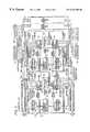
- FIG. 1is a block diagram of a computer system using a data storage system in accordance with the invention
- FIG. 2is a block diagram of an interface used in the data storage system of FIG. 1, such interface providing coupling between main frame computer processors and a bank of disk storage devices according to the invention;
- FIGS. 3A through 3Hare timing diagrams useful in understanding the operation of the data storage system interface of FIG. 2;
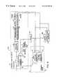
- FIG. 4is a block diagram of another interface adapted for use in the data storage system of FIG. 1, such interface providing coupling between main frame computer processors and a bank of disk storage devices according to the invention;
- FIGS. 5A through 5Hare timing diagrams useful in understanding the operation of the data storage system interface of FIG. 4 during a normal operating mode
- FIGS. 6A through 6Hare timing diagrams useful in understanding the operation of the data storage system interface of FIG. 4 during a copy operating mode
- FIG. 7is a block diagram showing a failure monitoring system according to the invention adapted for use with addressable memories adapted for use with the system shown in FIG. 1;
- FIG. 8is a block diagram showing an address parity bit checking system according to the invention adapted for use with addressable memories adapted for use with the system shown in FIG. 1 .
- the computer system 10includes a main frame computer section 12 having main frame processors 14 for processing data. Portions of the processed data are stored in, and retrieved data from, a bank 16 of disk drives 17 through an interface 18 .
- the interface 18includes disk controllers 20 , central processor unit (CPU) controllers 22 and addressable cache memories 24 a , 24 b electrically interconnected through a bus 25 , here a pair buses; i.e., an A bus 28 and a B bus 26 .
- the cache memories 24 a , 24 bare hereinafter sometimes referred to only as addressable memories.
- the pair of buses 26 , 28is provided.
- One portion of the disk controllers 20is connected to one of the buses 26 , 28 and the other portion of the disk controllers 20 is connected to the other one of the buses 26 , 28 .
- one portion of the CPU controllers 22is connected to one of the buses 26 , 28 and the other portion of the CPU controllers 22 is connected to the other one of the buses 26 , 28 .
- the cache memories 24 a , 24 bare connected to both buses 26 , 28 , as shown.
- each one of the addressable memories 24 a , 24 bincludes: a random access memory (RAM) 30 , here a dynamic random access memory (DRAM) adapted for coupling to bus 26 or bus 28 in response to row address select (RAS), column address select (CAS) write enable (W) and read enable (R) signals fed thereto; a pair of control logic networks 32 , 34 ; internal clock 36 ; and a pair of buffer memories 38 , 40 , all arranged as shown.
- RAMrandom access memory
- DRAMdynamic random access memory
- RASrow address select
- CAScolumn address select
- Wwrite enable
- Rread enable
- control logic network 32 and buffer memory 38are associated with bus 28 and control logic network 34 and buffer memory 40 are associated with bus 26 .
- a token arbitration systemis provided for controlling sharing of the pair of buses 26 , 28 by the common DRAM 30 .
- One such bus arbitration systemis described in co-pending patent application Ser. No. 08/534,376, “Bus Arbitration System, inventor Eli Leshem, filed Sep. 28, 1995, assigned to the same assignee as the present invention, the contents thereof being incorporated herein by reference.
- Each one of the buffer memories 38 , 40includes a write first-in/first-out memory (FIFO) 42 and a read FIFO 43 .
- the write FIFO 42 of buffer memory 38is adapted to have data written therein from the bus 28 in response to a write clock produced by the control logic network 32 ; such write clock being produced by network 32 in response to a bus write clock produced by a controller 20 , 22 on the bus 28 in a manner to be described in connection with FIGS. 3A through 3H.
- Data stored in the DRAM 30is supplied to bus 28 either indirectly through the read FIFO 43 of the buffer memory 38 , or directly via a by-pass, not shown.
- the write FIFO 42 of buffer memory 40is adapted to have data written therein from the bus 26 in response to a write clock produced by the control logic network 34 ; such write clock being produced by network 34 in response to a bus write clock produced by a controller 20 , 22 on the bus 26 in a manner equivalent to that to be described in connection with FIGS. 3A through 3H.
- Data stored in the DRAM 30is supplied to bus 26 either indirectly through the read FIFO 43 of the buffer memory 40 , or directly via a by-pass, not shown. It is noted that, while the internal transfer of data among the buffer memory 40 , DRAM 30 and bus 26 is controlled by control logic network 34 , both control logic networks 32 , 34 are synchronized with respect to each other by the internal clock 36 .
- bus arbitration for the shared DRAM 30is performed by the bus arbitration system described in the above referenced patent application.
- bus 28like bus 26 , has an bus-select/address/command portion 28 a and a bus-grant/data/clock-pulse portion 28 b , as shown in FIG. 2 .
- Each one of the controllers 20 , 22is adapted: (a) to assert on the bus-select/command/address portion 28 a of the bus 28 during a controller initiated bus assert interval (“BUS ASSERT”, FIG. 3 A), a command on bus portion 28 a (FIG. 3 B), such command including: (i) either a write operation request or a read operation request; and (ii) an address for the one of the addressable memories 24 a , 24 b selected by the controller 20 , 22 to respond to the write operation or read operation command; and (b) to produce data (FIG. 3E) and bus write clock pulses (FIG. 3F) on the bus-grant/data/clock-pulse portion 28 b of the bus 28 when a write operation is requested during a subsequent bus grant interval (FIG. 3C) produced by the addressed one of the memories 24 a , 24 b.
- a controller initiated bus assert interval(“BUS ASSERT”, FIG. 3 A)
- Each addressed one of the addressable cache memories 24 a , 24 bis adapted: (a) to produce on the bus-grant/data/clock-pulse portion 28 b of the bus 28 , a bus grant signal (FIG. 3C) to initiate the bus grant interval when the addressed one of the memories 24 a , 24 b is available to respond to the read or write operation request by the controller 20 , 22 (FIG. 3 B); (b) to provide on the bus-grant/data/clock-pulse portion 28 b of the bus 28 during the bus grant interval in response to the read operation request by the controller 20 , 22 : (i) data at the address provided by the controller 20 , 22 during the bus assert interval (FIGS.
- bus read clock pulses(FIG. 3 D); (c) to write, in response to the write operation request by the controller 20 , 22 during the bus grant interval, the data on the bus-grant/data/clock-pulse portion 28 b of the bus 28 into the addressed one of the memories 24 a , 24 b in response the bus write clock pulses produced by the controller 20 , 22 on the bus-grant/data/clock-pulse portion 28 b of the bus 28 ; and, (d) to remove the bus grant signal (FIG.
- Each one of the controllers 20 , 22is adapted to provide on the bus-select/address/command portion 28 a of the bus 28 another address and command after termination of a previous bus assertion interval.
- the control logic networks 32 , 34are configured to enable data on the bus 28 , 26 , respectively, to be written into the random access memory 50 of one of the addressed one of the memories 24 a , 24 b (here, for example, memory 24 a ) in response to clock pulses produced on the bus 28 , 26 , respectively during a period of time when data stored in the random access memory 50 of another one of the addressable memories 24 a , 24 b (here, in this example, memory 24 b ) is transferred to the buffer memory 38 , 40 , respectively, thereof in response to clock signals produced by the internal clock 36 thereof.
- data to be read from the other one of the addressable memoriescan be pre-fetched from the random access memory 50 thereof while data is written into the first-mentioned addressable memory (here, memory 24 a ).
- a controller 20 , 22asserts the bus 28 by changing the level of the signal on the bus-select/address/command portion 28 a of the bus 28 from a “high” to a “low”, FIG. 3 A.
- one of the addressable memories 24 a , 24 b , here memory 24 ais addressed, and a read command is requested by the controller 20 , 22 on the bus-select/address/command portion 28 a of the bus 28 .
- the addressed memory 24 ais granted the bus 28 and such memory 24 a changes the level on the bus-grant/data/clock-pulse portion 28 b of the bus 28 from a “high” to a “low”, FIG. 3 C. It is noted that once the memory grant has been placed on the bus-grant/data/clock-pulse portion 28 a of the bus 28 , a new bus select command may be issued by a controller 20 , 22 even during a bus grant interval. In this example, a new bus select is issued at time t 9 during the bus grant interval.
- a second controller selectwas asserted.
- the controller 20 , 22requests that memory 24 b write data on the bus 28 .
- memory 24 aOnce memory 24 a has completed its task, it de-asserts the bus grant at time t 4 .
- the memory 24 ais able to assert the bus 28 and, in this example, issues a bus grant signal at time t 5 .
- Data provided on the bus 28 (FIG. 3E) by the controller 20 , 22(along with clock pulses (FIG. 3 F)) is stored in the buffer memory 38 of memory 24 b , as shown in FIG. 3 H.
- a controller 20 , 22asserts the bus 28 .
- the asserting controller 20 , 22requests that data be read from memory 24 a .
- Memory 24 ais able to receive the request and, while memory 24 a is not able to transfer the requested data therein to the bus-grant/data/clock-pulse portion 28 b of the bus 28 because such bus has the data to be written into the memory 24 b , data in the DRAM 30 of memory 24 a can be read therefrom (i.e. pre-fetched) into the buffer memory 38 thereof.
- This pre-fetched data stored in the buffer 38is then placed on the bus 28 at time t 8 after the memory 24 b has released the bus 28 at time t 7 .
- This, pre-fetching processfrees the DRAM 30 for other requests, for example requests from B bus 26 which may occur as data is transferred from the buffer memory 38 to A bus 28 .
- each one of the addressable cache memories 24 ′ a , 24 ′ bincludes a master memory unit 50 and a slave memory unit 52 .
- Each one of the memory units 50 , 52has the same address as the addressable memory 24 a , 24 b thereof.
- the master memory unit 50 and slave memory unit 52 included in the addressable memory 24 aeach have the same address as the addressable memory 24 a .
- the master memory unit 50 and slave memory unit 52 included in the addressable memory 24 beach have the same address as the addressable memory 24 b.
- Each master memory unit 50 and slave memory unit 52includes: (1) a pair of buffer memories 38 , 40 coupled to the bus 28 , 26 , respectively, as shown; (2) a random access memory 30 coupled to the pair of buffer memories 38 , 40 , as shown; (3) an internal clock 36 ; and, (4) a pair of control logic networks 32 ′, 34 ′ coupled to the buses 28 , 26 , respectively, as shown, and configured to transfer data among the buffer memory 38 , 40 , respectively coupled thereto, the random access memory 30 and the bus 28 , 26 , respectively coupled thereto, as shown, in response to clock signals produced by the internal clock 36 and clock pulses provided on the bus 28 , 26 , respectively coupled thereto.
- the memory 24 a , 24 bdescribed in connection with FIG.
- control logic network 32 ′ and buffer memory 38are associated with bus 28 and control logic network 34 ′ and buffer memory 40 are associated with bus 26 .
- a token arbitration systemis provided for controlling sharing of the pair of buses 26 , 28 by the common DRAM 30 is described in the above-referenced co-pending patent application Ser. No. 08/534,376.
- each one of the buffer memories 38 , 40includes a write first-in/first-out memory (FIFO) 42 and a read FIFO 43 .
- the write FIFO 42 of buffer memory 38is adapted to have data written therein from the bus 28 in response to a write clock produced by the control logic network 32 ′; such write clock being produced by network 32 ′ in response to a bus write clock produced by a controller 20 , 22 on the bus 28 in a manner to be described in connection with FIGS. 5A through 5H.
- Data stored in the DRAM 30is supplied to bus 28 either indirectly through the read FIFO 43 of the buffer memory 38 , or directly via a by-pass, not shown.
- the write FIFO 42 of buffer memory 40is adapted to have data written therein from the bus 26 in response to a write clock produced by the control logic network 34 ′; such write clock being produced by network 34 ′ in response to a bus write clock produced by a controller 20 , 22 on the bus 26 in a manner equivalent to that to be described in connection with FIGS. 5A through 5H.
- Data stored in the DRAM 30is supplied to bus 26 either indirectly through the read FIFO 43 of the buffer memory 38 , or directly via a by-pass, not shown.
- control logic network 32 ′While the internal transfer of data among the buffer memory 38 , DRAM 30 and bus 28 is controlled by control logic network 32 ′, both control logic networks 32 ′, 34 ′ are synchronized with respect to each other by the internal clock 36 . It is noted that control logic network 32 ′ of the master memory unit 50 and the slave memory unit 52 are hereinafter sometimes jointly referred to as control unit 60 a . Likewise, control logic network 34 ′ of the master memory unit 50 and the slave memory unit 52 are hereinafter sometimes jointly referred to as control unit 60 b.
- bus 26operates in an equivalent manner, the pair of logic networks in each one of the addressable cache memories 24 a , 24 b provide a control unit 60 a therefor.
- Each addressable memory 24 a , 24 b control unit 60 a , 60 bis configured to produce control signals to enable data stored in the master memory unit 50 thereof to be read therefrom and transferred to the bus 28 , 26 , respectively, when such data is requested from the addressable memory 24 a , 24 b and to enable data on the bus 28 , 26 to be written into both the master memory unit 50 and the slave memory unit 52 when data on the bus 28 , 26 , respectively, is to be written into the addressable memory 24 a , 24 b.
- each control unit 60 a , 60 bis configured to produce control signals to control data transfer between the random access memory 30 and the bus-grant/data/clock-pulse portion 28 b , 26 b , respectively, of the bus 28 , 26 , respectively, as follows: (a) to enable data stored in the random access memory 30 of the master memory unit 50 to be read therefrom and transferred to the bus-grant/data/clock-pulse portion of the bus 28 b , 26 b , respectively, along with the produced bus read clock pulses when such data is requested by the controller 20 , 22 from the addressable memory 24 a , 24 b ; and, (b) to enable data on the bus-grant/data/clock-pulse portion 28 b , 26 b , of the bus 28 , 26 to be written concurrently into the random access memory 30 of both the master memory unit 50 and the slave memory unit 52 (since both the master memory unit 50 and the slave memory unit 52 have the same address as the addressable memory which includes such memory units
- FIGS. 5A through 5Hit is first noted that here the controller 20 , 22 produces the same requests as described above in connection with FIGS. 3A and 3B.
- the controller 20 , 22produces the same requests as described above in connection with FIGS. 3A and 3B.
- data in only the master memory unit 50is read during the bus grant interval (FIGS, 5 C, 5 D, 5 E and 5 F)
- data on the bus 28is written concurrently at time t 5 into both the master memory unit 50 and the slave memory unit 52 (FIGS, 5 G and 5 H; more particularly, into the buffer memories 38 of both the master memory unit 50 and the slave memory unit 52 ) in response to controller 20 , 22 produced write clock pulses (FIG. 5 F).
- the control logic unit 32 ′fails in either the master memory unit 50 or the slave memory unit 52 , the data is stored in the other one of the memory units 52 , 50 , respectively.
- control unit 60 a , 60 bis adapted to: (i) during a normal mode, enable data produced on the bus 28 , 26 to be written into both the master memory unit 50 and the slave memory unit 52 and data in only the master memory unit 50 to be read therefrom when such data is to be transferred to the bus 28 , 26 , and (ii) during a read/copy mode, enable data stored in the master memory unit 50 to be read therefrom, transferred to the bus 28 , 26 , and written from the bus 28 , 26 into the slave memory unit 52 .
- data in the master memory unit 50may be copied to the slave memory unit 52 after a failed slave memory unit 52 , for example, has been replaced without disrupting the operation of the system 10 .
- FIGS. 6A through 6Hit is first noted that here the controller 20 , 22 produces the same requests (FIGS. 6A and 6B) as described above in connection with FIGS. 3A and 3B.
- the new mater or slave unit control logic network 32 ′ or 34 ′is placed in the read/copy mode. Let it be assumed in this example that the slave unit 52 was replaced.
- a controller 20 , 22asserts here bus 28 and requests that memory 24 ′ a read data on the bus 28 .
- the addressed memory 24 ′ ais granted bus 28 , FIG. 6 C.
- the addressed memory 24 aproduces bus read clock pulses.
- FIG. 6 DData is transferred internally in the master memory unit 50 of the addressed memory 24 ′ a (FIG. 6G) from the DRAM 30 to the data portion 28 b of bus 28 (FIG. 6 E).
- FIG. 6Ethe data on the data portion 28 b of the bus (FIG. 6E) is written into both the master memory unit 50 and the slave memory unit 52 , since both memory units 50 , 52 have the same address as the memory 24 a , as shown in FIGS. 6E, 6 G and 6 H.
- a controller 20 , 22requests, for example, that memory 24 a read data on the data portion 28 b of the bus 28 .
- datais read internally in the master memory unit 50 of the addressed memory 24 a (FIG. 6G) and such read data is transferred to the data portion 28 b of bus 28 (FIG. 6 E).
- the data placed on the data portion 28 a of the bus 28is also copied into the buffer memory 38 of the slave memory unit 52 of the addressed memory 24 a , as shown in FIG. 6 H).
- control unit 60 a , 60 bprovides control signals to enable: (a) during a normal mode, data produced on the bus 28 , 26 , respectively, to be written into both the master memory unit 50 and the slave memory unit 52 in response to bus write clock pulses and data in only the master memory unit 50 to be read therefrom when such data is to be transferred to the bus 28 , 26 ; and (b) during a read/copy mode, data stored in the master memory unit 50 to read therefrom, transferred to the bus 28 , 26 , and written from the bus 28 , 26 into the slave memory unit 52 .
- addressable memory 24 ′ aadapted for use in system 10 (FIG. 1) as either the addressable memory 24 a shown in FIG. 2, or as a master memory unit 50 and/or slave memory unit 52 (FIG. 4) is shown. Elements in addressable memory 24 ′ a equivalent to those in memory 24 a have the same numerical designation.
- addressable memory 24 ′ aincludes, additionally, a failure monitoring system 59 ; more particularly, a pair of timer/logic units 60 a , 60 b .
- the timer/logic units 60 a , 60 bare provided to test whether the control signals produced by the control logic networks 32 , 34 are being produced properly.
- the A bus 28acquires the DRAM 30 and control logic network 32 produces an output enable signal, which is monitored on line 68 a , that allows A bus 28 to access the common DRAM 30 .
- the B bus 26acquires the DRAM 30 and control logic network 34 produces an output enable signal, which is monitored on line 68 b , that allows B bus 26 to access the common DRAM 30 .
- an active output enable signal produced by control logic network 32monitored on line 68 a by the timer/logic unit 60 a , indicates that the A bus 28 has access to the DRAM 30 and an active output enable signal produced by control logic network 34 , monitored on line 68 b by the timer/logic unit 60 b , indicates that the B bus 26 has access to the DRAM 30 .
- a token “A” or token “B” signalis passed between the control logic unit 32 and control logic unit 34 as described in the above reference patent application Ser. No. 08/534,376.
- the timer/logic unit 60 ameasures the time duration which the output enable signal is produced by control unit network 32 .
- the timer/logic unit 60 bmeasures the time duration which the output enable signal is produced by control unit network 34 .
- AND gates 69 a , 69 bare provided, the output of AND gate 69 a being fed to an enable input of driver 62 a and the output of AND gate 69 b being fed to the enable input of driver 62 b , as shown.
- the output enable signal produced by logic unit 32 on line 68 ais fed as one input to the AND gate 69 a and the output enable signal produced by logic unit 34 on line 68 b is fed as one input to the AND gate 62 b . If the output enable signal produced by control logic network 32 has been asserted for less than a predetermined maximum assertion time, here 10 microsecond, the AND gate 69 a enables the driver 62 a to pass the address signals from the control logic network 32 to the memory 30 . In like manner, if the output enable signal produced by control logic network 34 has been asserted for less than a predetermined maximum assertion time, here 10 microsecond, the AND gate 69 b enables the driver 62 b to pass the address signals from the control logic network 34 to the memory 30 .
- control logic network 34determines whether the output enable signal produced by control logic network 34 has been asserted for more than a predetermined maximum assertion time, here 10 microsecond, (i.e, the control logic network 32 is “stuck” in an DRAM/A bus 28 assert condition) the system 10 assumes a failure has occurred in the control logic network 32 .
- the AND gate 69 adisables the driver 62 a and inhibits the driver 62 a from passing the address signals from the control logic network 32 to the memory 30 .
- the timer/logic unit 60 aproduces a reset signal on line 70 a to reset the control logic network 32 and thereby advise the token, bus arbitration system that controller 32 no longer has the token.
- the reset signalis also fed to the control logic network 34 to advise it that there is no need for it to wait for a token from control logic unit 32 .
- the DRAM 30is enabled to be granted B bus 26 even if the bus arbitration system, not shown and referred to above, has not passed control to (i.e., a “token” to) such control logic network 34 .
- the timer/logic unitcounts the number of times a failure has occurred (i.e., the number of times within a predetermined period of time that the control logic network 32 is “stuck”) and if less than a predetermined number of times in the predetermined period of time, the timer/logic unit 60 a merely resets the control logic network 32 and not removed it from operation. Only when the control logic network 32 gets “stuck” more than the predetermined number of times within the predetermined period of time will the timer/logic unit 60 a permanently disable the control logic network 32 so that the DRAM will not be allowed access to the A bus 28 . In this case the control logic unit 32 must be replaced from the system 10 .
- control logic network 34if the output enable signal produced by control logic network 34 has been asserted for more than the predetermined maximum assertion time, here 10 microsecond, (i.e, the control logic network 34 is “stuck” in the assert condition) and the timer/logic unit 60 b will: (a) via AND gate 69 b disable the address driver 62 b ; and (b) reset the output assert signal in control logic network 32 thereby enabling the DRAM 30 to be granted A bus 28 even if the bus arbitration system, not shown, has not passed a “token” to such control logic network 32 .
- the predetermined maximum assertion timehere 10 microsecond
- the timer/logic unit 60 bIn order to account for a transient error in the control logic network 34 , the timer/logic unit 60 b counts the number of times a failure has occurred and if less than a predetermined number of times in the predetermined period of time, the timer/logic unit 60 b merely resets the control logic network 34 and does not removed it from operation. Only when the control logic network 34 gets “stuck” more than the predetermined number of times within the predetermined period of time will the timer/logic unit 60 b permanently disable the control logic network 34 so that the DRAM will not be allowed access to the B bus 26 . In this case the control logic unit 34 must be replaced from the system 10 .
- addressable memory 24 ′′ aadapted for use in system 10 (FIG. 1) as either the addressable memory 24 a shown in FIG. 2, or as a master memory unit 50 and/or slave memory unit 52 (FIG. 4) is shown. Elements in addressable memory 24 ′′ a equivalent to those in memory 24 a have the same numerical designation.
- addressable memory 24 ′′ aincludes, additionally, a system for determining whether there is a fault in the transmission of the address to the random access memory 30 via the address driver 62 a or 62 b .
- the control logic networks 32 , 34 and the random access memory 30include parity checking circuitry to be described. It is noted that while the details of the parity checking circuity are shown and will be described for control logic network 32 , it should be understood that control logic network 34 has the equivalent parity checking circuit and operates in the equivalent manner.
- control logic network 32receives the full, parallel address on A bus 28 . That is, the address on bus 28 includes both the row address portion and the column address portion for the random access memory 30 in parallel.
- the full, parallel address on bus 28is fed to a selector 100 .
- RASrow address select
- CAScolumn address select
- control logic network 32includes a parity bit generator 102 fed by the output of the selector 100 and the control signal for such selector 100 for generating a row parity bit from the row address signal portion of the address on bus 28 and a column parity bit from the column address signal portion of the address on bus 28 .
- the generated row address parity bitis stored in row address parity bit register 104 and the generated column parity bit is stored in column register 106 .
- the address driver 62 afeeds the sequence of the row address signal and the column address signal produced by the control logic network 32 to the random access memory 30 .
- the random access memory 30includes a row parity bit generator 108 for producing a parity bit from the row address fed thereto by the address driver 62 a and a column parity bit generator 110 for producing a parity bit from the column address fed thereto by the address driver 62 a .
- the row and column parity bits produced by the generators 108 , 110are fed to the control logic network 32 and compared with the row and column parity bits, respectively, generated by the control logic network 32 in comparators 112 , 114 , respectively.
Landscapes
- Engineering & Computer Science (AREA)
- Theoretical Computer Science (AREA)
- Physics & Mathematics (AREA)
- General Engineering & Computer Science (AREA)
- General Physics & Mathematics (AREA)
- Quality & Reliability (AREA)
- Memory System Of A Hierarchy Structure (AREA)
Abstract
Description
Claims (6)
Priority Applications (2)
| Application Number | Priority Date | Filing Date | Title |
|---|---|---|---|
| US08/701,917US6567903B1 (en) | 1996-08-23 | 1996-08-23 | Data storage system having master/slave addressable memories |
| US08/701,981US6347365B1 (en) | 1996-08-23 | 1996-08-23 | Data storage system having a[n] memory responsive to clock pulses produced on a bus and clock pulses produced by an internal clock |
Applications Claiming Priority (2)
| Application Number | Priority Date | Filing Date | Title |
|---|---|---|---|
| US08/701,917US6567903B1 (en) | 1996-08-23 | 1996-08-23 | Data storage system having master/slave addressable memories |
| US08/701,981US6347365B1 (en) | 1996-08-23 | 1996-08-23 | Data storage system having a[n] memory responsive to clock pulses produced on a bus and clock pulses produced by an internal clock |
Publications (1)
| Publication Number | Publication Date |
|---|---|
| US6347365B1true US6347365B1 (en) | 2002-02-12 |
Family
ID=46276151
Family Applications (1)
| Application Number | Title | Priority Date | Filing Date |
|---|---|---|---|
| US08/701,981Expired - LifetimeUS6347365B1 (en) | 1996-08-23 | 1996-08-23 | Data storage system having a[n] memory responsive to clock pulses produced on a bus and clock pulses produced by an internal clock |
Country Status (1)
| Country | Link |
|---|---|
| US (1) | US6347365B1 (en) |
Cited By (15)
| Publication number | Priority date | Publication date | Assignee | Title |
|---|---|---|---|---|
| US20050065962A1 (en)* | 2003-09-23 | 2005-03-24 | Revivio, Inc. | Virtual data store creation and use |
| US20050066118A1 (en)* | 2003-09-23 | 2005-03-24 | Robert Perry | Methods and apparatus for recording write requests directed to a data store |
| US20050063374A1 (en)* | 2003-09-23 | 2005-03-24 | Revivio, Inc. | Method for identifying the time at which data was written to a data store |
| US20050066225A1 (en)* | 2003-09-23 | 2005-03-24 | Michael Rowan | Data storage system |
| US20050076264A1 (en)* | 2003-09-23 | 2005-04-07 | Michael Rowan | Methods and devices for restoring a portion of a data store |
| US20060047895A1 (en)* | 2004-08-24 | 2006-03-02 | Michael Rowan | Systems and methods for providing a modification history for a location within a data store |
| US20060047903A1 (en)* | 2004-08-24 | 2006-03-02 | Ron Passerini | Systems, apparatus, and methods for processing I/O requests |
| US20060047902A1 (en)* | 2004-08-24 | 2006-03-02 | Ron Passerini | Processing storage-related I/O requests using binary tree data structures |
| US20060047989A1 (en)* | 2004-08-24 | 2006-03-02 | Diane Delgado | Systems and methods for synchronizing the internal clocks of a plurality of processor modules |
| US20060047998A1 (en)* | 2004-08-24 | 2006-03-02 | Jeff Darcy | Methods and apparatus for optimally selecting a storage buffer for the storage of data |
| US20060047999A1 (en)* | 2004-08-24 | 2006-03-02 | Ron Passerini | Generation and use of a time map for accessing a prior image of a storage device |
| US20060047925A1 (en)* | 2004-08-24 | 2006-03-02 | Robert Perry | Recovering from storage transaction failures using checkpoints |
| US20070088973A1 (en)* | 2005-10-14 | 2007-04-19 | Revivio, Inc. | Technique for timeline compression in a data store |
| US20110271347A1 (en)* | 2003-05-19 | 2011-11-03 | Zimmer Vincent J | Pre-boot firmware based virus scanner |
| US20130033390A1 (en)* | 2011-08-01 | 2013-02-07 | Mitsubishi Electric Corporation | Analog input system, analog output system, and analog input/output system |
Citations (28)
| Publication number | Priority date | Publication date | Assignee | Title |
|---|---|---|---|---|
| USRE30331E (en)* | 1973-08-10 | 1980-07-08 | Data General Corporation | Data processing system having a unique CPU and memory timing relationship and data path configuration |
| US4340964A (en) | 1979-06-27 | 1982-07-20 | Siemens Aktiengesellschaft | Method and an arrangement for automatic access optimization in random access memories |
| US4709327A (en)* | 1983-05-31 | 1987-11-24 | Hillis W Daniel | Parallel processor/memory circuit |
| US5005151A (en) | 1988-05-13 | 1991-04-02 | Dallas Semiconductor Corporation | Interleaved arbitration scheme for interfacing parallel and serial ports to a parallel system port |
| US5187794A (en)* | 1989-03-15 | 1993-02-16 | The United States Of America As Represented By The Administrator Of The National Aeronautics And Space Administration | System for simultaneously loading program to master computer memory devices and corresponding slave computer memory devices |
| US5206939A (en)* | 1990-09-24 | 1993-04-27 | Emc Corporation | System and method for disk mapping and data retrieval |
| US5208779A (en)* | 1991-04-15 | 1993-05-04 | Micron Technology, Inc. | Circuit for providing synchronous refresh cycles in self-refreshing interruptable DRAMs |
| US5224214A (en)* | 1990-04-12 | 1993-06-29 | Digital Equipment Corp. | BuIffet for gathering write requests and resolving read conflicts by matching read and write requests |
| US5265234A (en)* | 1985-05-20 | 1993-11-23 | Hitachi, Ltd. | Integrated memory circuit and function unit with selective storage of logic functions |
| US5276858A (en) | 1991-12-26 | 1994-01-04 | Intel Corporation | Memory controller with integrated delay line circuitry |
| US5432922A (en) | 1993-08-23 | 1995-07-11 | International Business Machines Corporation | Digital storage system and method having alternating deferred updating of mirrored storage disks |
| US5469558A (en) | 1991-08-16 | 1995-11-21 | Multichip Technology | Dynamically reconfigurable memory system with programmable controller and FIFO buffered data channels |
| US5488731A (en) | 1992-08-03 | 1996-01-30 | International Business Machines Corporation | Synchronization method for loosely coupled arrays of redundant disk drives |
| US5499353A (en)* | 1993-03-30 | 1996-03-12 | Ast Research, Inc. | Cache address strobe control logic for stimulated bus cycle initiation |
| US5539345A (en) | 1992-12-30 | 1996-07-23 | Digital Equipment Corporation | Phase detector apparatus |
| US5638535A (en) | 1995-05-15 | 1997-06-10 | Nvidia Corporation | Method and apparatus for providing flow control with lying for input/output operations in a computer system |
| US5649096A (en) | 1993-11-22 | 1997-07-15 | Unisys Corporation | Bus request error detection |
| US5655113A (en) | 1994-07-05 | 1997-08-05 | Monolithic System Technology, Inc. | Resynchronization circuit for a memory system and method of operating same |
| US5657467A (en)* | 1993-03-18 | 1997-08-12 | Fujitsu Limited | Non-volatile semiconductor memory device with instruction issue during busy cycle |
| US5659690A (en)* | 1992-10-15 | 1997-08-19 | Adaptec, Inc. | Programmably configurable host adapter integrated circuit including a RISC processor |
| US5740397A (en) | 1995-10-11 | 1998-04-14 | Arco Computer Products, Inc. | IDE disk drive adapter for computer backup and fault tolerance |
| US5754838A (en)* | 1994-12-27 | 1998-05-19 | Hitachi, Ltd. | Synchronous dynamic memory device capable of operating over wide range of operation frequencies |
| US5784548A (en)* | 1996-03-08 | 1998-07-21 | Mylex Corporation | Modular mirrored cache memory battery backup system |
| US5787265A (en) | 1995-09-28 | 1998-07-28 | Emc Corporation | Bus arbitration system having a pair of logic networks to control data transfer between a memory and a pair of buses |
| US5809543A (en)* | 1993-12-23 | 1998-09-15 | Unisys Corporation | Fault tolerant extended processing complex for redundant nonvolatile file caching |
| US5812822A (en) | 1995-12-19 | 1998-09-22 | Selway; David W. | Apparatus for coordinating clock oscillators in a fully redundant computer system |
| US5828820A (en) | 1995-05-10 | 1998-10-27 | Mitsubishi Denki Kabushiki Kaisha | Mirror disk control method and mirror disk device |
| US5991861A (en)* | 1996-03-15 | 1999-11-23 | Adaptec, Inc. | Method of enabling and disabling a data function in an integrated circuit |
- 1996
- 1996-08-23USUS08/701,981patent/US6347365B1/ennot_activeExpired - Lifetime
Patent Citations (28)
| Publication number | Priority date | Publication date | Assignee | Title |
|---|---|---|---|---|
| USRE30331E (en)* | 1973-08-10 | 1980-07-08 | Data General Corporation | Data processing system having a unique CPU and memory timing relationship and data path configuration |
| US4340964A (en) | 1979-06-27 | 1982-07-20 | Siemens Aktiengesellschaft | Method and an arrangement for automatic access optimization in random access memories |
| US4709327A (en)* | 1983-05-31 | 1987-11-24 | Hillis W Daniel | Parallel processor/memory circuit |
| US5265234A (en)* | 1985-05-20 | 1993-11-23 | Hitachi, Ltd. | Integrated memory circuit and function unit with selective storage of logic functions |
| US5005151A (en) | 1988-05-13 | 1991-04-02 | Dallas Semiconductor Corporation | Interleaved arbitration scheme for interfacing parallel and serial ports to a parallel system port |
| US5187794A (en)* | 1989-03-15 | 1993-02-16 | The United States Of America As Represented By The Administrator Of The National Aeronautics And Space Administration | System for simultaneously loading program to master computer memory devices and corresponding slave computer memory devices |
| US5224214A (en)* | 1990-04-12 | 1993-06-29 | Digital Equipment Corp. | BuIffet for gathering write requests and resolving read conflicts by matching read and write requests |
| US5206939A (en)* | 1990-09-24 | 1993-04-27 | Emc Corporation | System and method for disk mapping and data retrieval |
| US5208779A (en)* | 1991-04-15 | 1993-05-04 | Micron Technology, Inc. | Circuit for providing synchronous refresh cycles in self-refreshing interruptable DRAMs |
| US5469558A (en) | 1991-08-16 | 1995-11-21 | Multichip Technology | Dynamically reconfigurable memory system with programmable controller and FIFO buffered data channels |
| US5276858A (en) | 1991-12-26 | 1994-01-04 | Intel Corporation | Memory controller with integrated delay line circuitry |
| US5488731A (en) | 1992-08-03 | 1996-01-30 | International Business Machines Corporation | Synchronization method for loosely coupled arrays of redundant disk drives |
| US5659690A (en)* | 1992-10-15 | 1997-08-19 | Adaptec, Inc. | Programmably configurable host adapter integrated circuit including a RISC processor |
| US5539345A (en) | 1992-12-30 | 1996-07-23 | Digital Equipment Corporation | Phase detector apparatus |
| US5657467A (en)* | 1993-03-18 | 1997-08-12 | Fujitsu Limited | Non-volatile semiconductor memory device with instruction issue during busy cycle |
| US5499353A (en)* | 1993-03-30 | 1996-03-12 | Ast Research, Inc. | Cache address strobe control logic for stimulated bus cycle initiation |
| US5432922A (en) | 1993-08-23 | 1995-07-11 | International Business Machines Corporation | Digital storage system and method having alternating deferred updating of mirrored storage disks |
| US5649096A (en) | 1993-11-22 | 1997-07-15 | Unisys Corporation | Bus request error detection |
| US5809543A (en)* | 1993-12-23 | 1998-09-15 | Unisys Corporation | Fault tolerant extended processing complex for redundant nonvolatile file caching |
| US5655113A (en) | 1994-07-05 | 1997-08-05 | Monolithic System Technology, Inc. | Resynchronization circuit for a memory system and method of operating same |
| US5754838A (en)* | 1994-12-27 | 1998-05-19 | Hitachi, Ltd. | Synchronous dynamic memory device capable of operating over wide range of operation frequencies |
| US5828820A (en) | 1995-05-10 | 1998-10-27 | Mitsubishi Denki Kabushiki Kaisha | Mirror disk control method and mirror disk device |
| US5638535A (en) | 1995-05-15 | 1997-06-10 | Nvidia Corporation | Method and apparatus for providing flow control with lying for input/output operations in a computer system |
| US5787265A (en) | 1995-09-28 | 1998-07-28 | Emc Corporation | Bus arbitration system having a pair of logic networks to control data transfer between a memory and a pair of buses |
| US5740397A (en) | 1995-10-11 | 1998-04-14 | Arco Computer Products, Inc. | IDE disk drive adapter for computer backup and fault tolerance |
| US5812822A (en) | 1995-12-19 | 1998-09-22 | Selway; David W. | Apparatus for coordinating clock oscillators in a fully redundant computer system |
| US5784548A (en)* | 1996-03-08 | 1998-07-21 | Mylex Corporation | Modular mirrored cache memory battery backup system |
| US5991861A (en)* | 1996-03-15 | 1999-11-23 | Adaptec, Inc. | Method of enabling and disabling a data function in an integrated circuit |
Non-Patent Citations (1)
| Title |
|---|
| Co-Pending U.S. Patent Application Serial No. 08/701,917, filed August 23, 1996 and Assigned to Art Unit 2752, Examiner D. Ransom. |
Cited By (41)
| Publication number | Priority date | Publication date | Assignee | Title |
|---|---|---|---|---|
| US9710647B2 (en)* | 2003-05-19 | 2017-07-18 | Intel Corporation | Pre-boot firmware based virus scanner |
| US20110271347A1 (en)* | 2003-05-19 | 2011-11-03 | Zimmer Vincent J | Pre-boot firmware based virus scanner |
| US8364974B2 (en)* | 2003-05-19 | 2013-01-29 | Intel Corporation | Pre-boot firmware based virus scanner |
| US20130205395A1 (en)* | 2003-05-19 | 2013-08-08 | Vincent J. Zimmer | Pre-boot firmware based virus scanner |
| US20050066222A1 (en)* | 2003-09-23 | 2005-03-24 | Revivio, Inc. | Systems and methods for time dependent data storage and recovery |
| US20050066118A1 (en)* | 2003-09-23 | 2005-03-24 | Robert Perry | Methods and apparatus for recording write requests directed to a data store |
| US20050076264A1 (en)* | 2003-09-23 | 2005-04-07 | Michael Rowan | Methods and devices for restoring a portion of a data store |
| US7577807B2 (en) | 2003-09-23 | 2009-08-18 | Symantec Operating Corporation | Methods and devices for restoring a portion of a data store |
| US20050066225A1 (en)* | 2003-09-23 | 2005-03-24 | Michael Rowan | Data storage system |
| US20050063374A1 (en)* | 2003-09-23 | 2005-03-24 | Revivio, Inc. | Method for identifying the time at which data was written to a data store |
| US20050065962A1 (en)* | 2003-09-23 | 2005-03-24 | Revivio, Inc. | Virtual data store creation and use |
| US20050076261A1 (en)* | 2003-09-23 | 2005-04-07 | Revivio, Inc. | Method and system for obtaining data stored in a data store |
| US7991748B2 (en) | 2003-09-23 | 2011-08-02 | Symantec Corporation | Virtual data store creation and use |
| US7904428B2 (en) | 2003-09-23 | 2011-03-08 | Symantec Corporation | Methods and apparatus for recording write requests directed to a data store |
| US7725760B2 (en) | 2003-09-23 | 2010-05-25 | Symantec Operating Corporation | Data storage system |
| US7725667B2 (en) | 2003-09-23 | 2010-05-25 | Symantec Operating Corporation | Method for identifying the time at which data was written to a data store |
| US7272666B2 (en) | 2003-09-23 | 2007-09-18 | Symantec Operating Corporation | Storage management device |
| US7584337B2 (en) | 2003-09-23 | 2009-09-01 | Symantec Operating Corporation | Method and system for obtaining data stored in a data store |
| US7577806B2 (en) | 2003-09-23 | 2009-08-18 | Symantec Operating Corporation | Systems and methods for time dependent data storage and recovery |
| US20060047989A1 (en)* | 2004-08-24 | 2006-03-02 | Diane Delgado | Systems and methods for synchronizing the internal clocks of a plurality of processor modules |
| US20060047925A1 (en)* | 2004-08-24 | 2006-03-02 | Robert Perry | Recovering from storage transaction failures using checkpoints |
| US20060047895A1 (en)* | 2004-08-24 | 2006-03-02 | Michael Rowan | Systems and methods for providing a modification history for a location within a data store |
| US7409587B2 (en) | 2004-08-24 | 2008-08-05 | Symantec Operating Corporation | Recovering from storage transaction failures using checkpoints |
| US7296008B2 (en) | 2004-08-24 | 2007-11-13 | Symantec Operating Corporation | Generation and use of a time map for accessing a prior image of a storage device |
| US7287133B2 (en) | 2004-08-24 | 2007-10-23 | Symantec Operating Corporation | Systems and methods for providing a modification history for a location within a data store |
| US7631120B2 (en) | 2004-08-24 | 2009-12-08 | Symantec Operating Corporation | Methods and apparatus for optimally selecting a storage buffer for the storage of data |
| US7239581B2 (en) | 2004-08-24 | 2007-07-03 | Symantec Operating Corporation | Systems and methods for synchronizing the internal clocks of a plurality of processor modules |
| US8521973B2 (en) | 2004-08-24 | 2013-08-27 | Symantec Operating Corporation | Systems and methods for providing a modification history for a location within a data store |
| US7730222B2 (en) | 2004-08-24 | 2010-06-01 | Symantec Operating System | Processing storage-related I/O requests using binary tree data structures |
| US7827362B2 (en) | 2004-08-24 | 2010-11-02 | Symantec Corporation | Systems, apparatus, and methods for processing I/O requests |
| US20090019459A1 (en)* | 2004-08-24 | 2009-01-15 | Symantec Operating Corporation | Systems and methods for providing a modification history for a location within a data store |
| US20060047999A1 (en)* | 2004-08-24 | 2006-03-02 | Ron Passerini | Generation and use of a time map for accessing a prior image of a storage device |
| US20060047998A1 (en)* | 2004-08-24 | 2006-03-02 | Jeff Darcy | Methods and apparatus for optimally selecting a storage buffer for the storage of data |
| US20060047902A1 (en)* | 2004-08-24 | 2006-03-02 | Ron Passerini | Processing storage-related I/O requests using binary tree data structures |
| US20060047903A1 (en)* | 2004-08-24 | 2006-03-02 | Ron Passerini | Systems, apparatus, and methods for processing I/O requests |
| US20070088973A1 (en)* | 2005-10-14 | 2007-04-19 | Revivio, Inc. | Technique for timeline compression in a data store |
| US7536583B2 (en) | 2005-10-14 | 2009-05-19 | Symantec Operating Corporation | Technique for timeline compression in a data store |
| CN103039007A (en)* | 2011-08-01 | 2013-04-10 | 三菱电机株式会社 | Analog input system, analog output system, and analog input and output system |
| US20130033390A1 (en)* | 2011-08-01 | 2013-02-07 | Mitsubishi Electric Corporation | Analog input system, analog output system, and analog input/output system |
| US8564466B2 (en)* | 2011-08-01 | 2013-10-22 | Mitsubishi Electric Corporation | Analog input system, analog output system, and analog input/output system |
| CN103039007B (en)* | 2011-08-01 | 2016-01-06 | 三菱电机株式会社 | Analog input system, modulating output system and analog input output system |
Similar Documents
| Publication | Publication Date | Title |
|---|---|---|
| US5822777A (en) | Dual bus data storage system having an addressable memory with timer controller fault detection of data transfer between the memory and the buses | |
| US5313627A (en) | Parity error detection and recovery | |
| US6347365B1 (en) | Data storage system having a[n] memory responsive to clock pulses produced on a bus and clock pulses produced by an internal clock | |
| US5255374A (en) | Bus interface logic for computer system having dual bus architecture | |
| US7434081B2 (en) | System and method for read synchronization of memory modules | |
| US5499346A (en) | Bus-to-bus bridge for a multiple bus information handling system that optimizes data transfers between a system bus and a peripheral bus | |
| US5699510A (en) | Failure detection system for a mirrored memory dual controller disk storage system | |
| US5249284A (en) | Method and system for maintaining data coherency between main and cache memories | |
| EP0817054A2 (en) | Simultaneous, mirror write cache | |
| US20060218331A1 (en) | System and method for communicating the synchronization status of memory modules during initialization of the memory modules | |
| US6493795B1 (en) | Data storage system | |
| JPH01154243A (en) | Interface between non failure-proof element and failure-proof system | |
| US6195770B1 (en) | Data storage system | |
| US5991852A (en) | Cache ram using a secondary controller and switching circuit and improved chassis arrangement | |
| US5687393A (en) | System for controlling responses to requests over a data bus between a plurality of master controllers and a slave storage controller by inserting control characters | |
| US6397281B1 (en) | Bus arbitration system | |
| US6145042A (en) | Timing protocol for a data storage system | |
| US5089953A (en) | Control and arbitration unit | |
| CA2119228C (en) | Arrangement for expanding the device capacity of a bus | |
| US5850528A (en) | Bus timing protocol for a data storage system | |
| US5954838A (en) | Data storage system having row/column address parity checking | |
| US6327676B1 (en) | Test equipment | |
| US6567903B1 (en) | Data storage system having master/slave addressable memories | |
| US6502149B2 (en) | Plural bus data storage system | |
| US5204964A (en) | Method and apparatus for resetting a memory upon power recovery |
Legal Events
| Date | Code | Title | Description |
|---|---|---|---|
| AS | Assignment | Owner name:EMC CORPORATION, MASSACHUSETTS Free format text:ASSIGNMENT OF ASSIGNORS INTEREST;ASSIGNORS:LESHEM, ELI;WALTON, JOHN K.;REEL/FRAME:008223/0104 Effective date:19961031 | |
| STCF | Information on status: patent grant | Free format text:PATENTED CASE | |
| FPAY | Fee payment | Year of fee payment:4 | |
| FPAY | Fee payment | Year of fee payment:8 | |
| FPAY | Fee payment | Year of fee payment:12 | |
| AS | Assignment | Owner name:THE BANK OF NEW YORK MELLON TRUST COMPANY, N.A., AS NOTES COLLATERAL AGENT, TEXAS Free format text:SECURITY AGREEMENT;ASSIGNORS:ASAP SOFTWARE EXPRESS, INC.;AVENTAIL LLC;CREDANT TECHNOLOGIES, INC.;AND OTHERS;REEL/FRAME:040136/0001 Effective date:20160907 Owner name:CREDIT SUISSE AG, CAYMAN ISLANDS BRANCH, AS COLLATERAL AGENT, NORTH CAROLINA Free format text:SECURITY AGREEMENT;ASSIGNORS:ASAP SOFTWARE EXPRESS, INC.;AVENTAIL LLC;CREDANT TECHNOLOGIES, INC.;AND OTHERS;REEL/FRAME:040134/0001 Effective date:20160907 Owner name:CREDIT SUISSE AG, CAYMAN ISLANDS BRANCH, AS COLLAT Free format text:SECURITY AGREEMENT;ASSIGNORS:ASAP SOFTWARE EXPRESS, INC.;AVENTAIL LLC;CREDANT TECHNOLOGIES, INC.;AND OTHERS;REEL/FRAME:040134/0001 Effective date:20160907 Owner name:THE BANK OF NEW YORK MELLON TRUST COMPANY, N.A., A Free format text:SECURITY AGREEMENT;ASSIGNORS:ASAP SOFTWARE EXPRESS, INC.;AVENTAIL LLC;CREDANT TECHNOLOGIES, INC.;AND OTHERS;REEL/FRAME:040136/0001 Effective date:20160907 | |
| AS | Assignment | Owner name:EMC IP HOLDING COMPANY LLC, MASSACHUSETTS Free format text:ASSIGNMENT OF ASSIGNORS INTEREST;ASSIGNOR:EMC CORPORATION;REEL/FRAME:040203/0001 Effective date:20160906 | |
| AS | Assignment | Owner name:WYSE TECHNOLOGY L.L.C., CALIFORNIA Free format text:RELEASE BY SECURED PARTY;ASSIGNOR:CREDIT SUISSE AG, CAYMAN ISLANDS BRANCH;REEL/FRAME:058216/0001 Effective date:20211101 Owner name:SCALEIO LLC, MASSACHUSETTS Free format text:RELEASE BY SECURED PARTY;ASSIGNOR:CREDIT SUISSE AG, CAYMAN ISLANDS BRANCH;REEL/FRAME:058216/0001 Effective date:20211101 Owner name:MOZY, INC., WASHINGTON Free format text:RELEASE BY SECURED PARTY;ASSIGNOR:CREDIT SUISSE AG, CAYMAN ISLANDS BRANCH;REEL/FRAME:058216/0001 Effective date:20211101 Owner name:MAGINATICS LLC, CALIFORNIA Free format text:RELEASE BY SECURED PARTY;ASSIGNOR:CREDIT SUISSE AG, CAYMAN ISLANDS BRANCH;REEL/FRAME:058216/0001 Effective date:20211101 Owner name:FORCE10 NETWORKS, INC., CALIFORNIA Free format text:RELEASE BY SECURED PARTY;ASSIGNOR:CREDIT SUISSE AG, CAYMAN ISLANDS BRANCH;REEL/FRAME:058216/0001 Effective date:20211101 Owner name:EMC IP HOLDING COMPANY LLC, TEXAS Free format text:RELEASE BY SECURED PARTY;ASSIGNOR:CREDIT SUISSE AG, CAYMAN ISLANDS BRANCH;REEL/FRAME:058216/0001 Effective date:20211101 Owner name:EMC CORPORATION, MASSACHUSETTS Free format text:RELEASE BY SECURED PARTY;ASSIGNOR:CREDIT SUISSE AG, CAYMAN ISLANDS BRANCH;REEL/FRAME:058216/0001 Effective date:20211101 Owner name:DELL SYSTEMS CORPORATION, TEXAS Free format text:RELEASE BY SECURED PARTY;ASSIGNOR:CREDIT SUISSE AG, CAYMAN ISLANDS BRANCH;REEL/FRAME:058216/0001 Effective date:20211101 Owner name:DELL SOFTWARE INC., CALIFORNIA Free format text:RELEASE BY SECURED PARTY;ASSIGNOR:CREDIT SUISSE AG, CAYMAN ISLANDS BRANCH;REEL/FRAME:058216/0001 Effective date:20211101 Owner name:DELL PRODUCTS L.P., TEXAS Free format text:RELEASE BY SECURED PARTY;ASSIGNOR:CREDIT SUISSE AG, CAYMAN ISLANDS BRANCH;REEL/FRAME:058216/0001 Effective date:20211101 Owner name:DELL MARKETING L.P., TEXAS Free format text:RELEASE BY SECURED PARTY;ASSIGNOR:CREDIT SUISSE AG, CAYMAN ISLANDS BRANCH;REEL/FRAME:058216/0001 Effective date:20211101 Owner name:DELL INTERNATIONAL, L.L.C., TEXAS Free format text:RELEASE BY SECURED PARTY;ASSIGNOR:CREDIT SUISSE AG, CAYMAN ISLANDS BRANCH;REEL/FRAME:058216/0001 Effective date:20211101 Owner name:DELL USA L.P., TEXAS Free format text:RELEASE BY SECURED PARTY;ASSIGNOR:CREDIT SUISSE AG, CAYMAN ISLANDS BRANCH;REEL/FRAME:058216/0001 Effective date:20211101 Owner name:CREDANT TECHNOLOGIES, INC., TEXAS Free format text:RELEASE BY SECURED PARTY;ASSIGNOR:CREDIT SUISSE AG, CAYMAN ISLANDS BRANCH;REEL/FRAME:058216/0001 Effective date:20211101 Owner name:AVENTAIL LLC, CALIFORNIA Free format text:RELEASE BY SECURED PARTY;ASSIGNOR:CREDIT SUISSE AG, CAYMAN ISLANDS BRANCH;REEL/FRAME:058216/0001 Effective date:20211101 Owner name:ASAP SOFTWARE EXPRESS, INC., ILLINOIS Free format text:RELEASE BY SECURED PARTY;ASSIGNOR:CREDIT SUISSE AG, CAYMAN ISLANDS BRANCH;REEL/FRAME:058216/0001 Effective date:20211101 | |
| AS | Assignment | Owner name:SCALEIO LLC, MASSACHUSETTS Free format text:RELEASE OF SECURITY INTEREST IN PATENTS PREVIOUSLY RECORDED AT REEL/FRAME (040136/0001);ASSIGNOR:THE BANK OF NEW YORK MELLON TRUST COMPANY, N.A., AS NOTES COLLATERAL AGENT;REEL/FRAME:061324/0001 Effective date:20220329 Owner name:EMC IP HOLDING COMPANY LLC (ON BEHALF OF ITSELF AND AS SUCCESSOR-IN-INTEREST TO MOZY, INC.), TEXAS Free format text:RELEASE OF SECURITY INTEREST IN PATENTS PREVIOUSLY RECORDED AT REEL/FRAME (040136/0001);ASSIGNOR:THE BANK OF NEW YORK MELLON TRUST COMPANY, N.A., AS NOTES COLLATERAL AGENT;REEL/FRAME:061324/0001 Effective date:20220329 Owner name:EMC CORPORATION (ON BEHALF OF ITSELF AND AS SUCCESSOR-IN-INTEREST TO MAGINATICS LLC), MASSACHUSETTS Free format text:RELEASE OF SECURITY INTEREST IN PATENTS PREVIOUSLY RECORDED AT REEL/FRAME (040136/0001);ASSIGNOR:THE BANK OF NEW YORK MELLON TRUST COMPANY, N.A., AS NOTES COLLATERAL AGENT;REEL/FRAME:061324/0001 Effective date:20220329 Owner name:DELL MARKETING CORPORATION (SUCCESSOR-IN-INTEREST TO FORCE10 NETWORKS, INC. AND WYSE TECHNOLOGY L.L.C.), TEXAS Free format text:RELEASE OF SECURITY INTEREST IN PATENTS PREVIOUSLY RECORDED AT REEL/FRAME (040136/0001);ASSIGNOR:THE BANK OF NEW YORK MELLON TRUST COMPANY, N.A., AS NOTES COLLATERAL AGENT;REEL/FRAME:061324/0001 Effective date:20220329 Owner name:DELL PRODUCTS L.P., TEXAS Free format text:RELEASE OF SECURITY INTEREST IN PATENTS PREVIOUSLY RECORDED AT REEL/FRAME (040136/0001);ASSIGNOR:THE BANK OF NEW YORK MELLON TRUST COMPANY, N.A., AS NOTES COLLATERAL AGENT;REEL/FRAME:061324/0001 Effective date:20220329 Owner name:DELL INTERNATIONAL L.L.C., TEXAS Free format text:RELEASE OF SECURITY INTEREST IN PATENTS PREVIOUSLY RECORDED AT REEL/FRAME (040136/0001);ASSIGNOR:THE BANK OF NEW YORK MELLON TRUST COMPANY, N.A., AS NOTES COLLATERAL AGENT;REEL/FRAME:061324/0001 Effective date:20220329 Owner name:DELL USA L.P., TEXAS Free format text:RELEASE OF SECURITY INTEREST IN PATENTS PREVIOUSLY RECORDED AT REEL/FRAME (040136/0001);ASSIGNOR:THE BANK OF NEW YORK MELLON TRUST COMPANY, N.A., AS NOTES COLLATERAL AGENT;REEL/FRAME:061324/0001 Effective date:20220329 Owner name:DELL MARKETING L.P. (ON BEHALF OF ITSELF AND AS SUCCESSOR-IN-INTEREST TO CREDANT TECHNOLOGIES, INC.), TEXAS Free format text:RELEASE OF SECURITY INTEREST IN PATENTS PREVIOUSLY RECORDED AT REEL/FRAME (040136/0001);ASSIGNOR:THE BANK OF NEW YORK MELLON TRUST COMPANY, N.A., AS NOTES COLLATERAL AGENT;REEL/FRAME:061324/0001 Effective date:20220329 Owner name:DELL MARKETING CORPORATION (SUCCESSOR-IN-INTEREST TO ASAP SOFTWARE EXPRESS, INC.), TEXAS Free format text:RELEASE OF SECURITY INTEREST IN PATENTS PREVIOUSLY RECORDED AT REEL/FRAME (040136/0001);ASSIGNOR:THE BANK OF NEW YORK MELLON TRUST COMPANY, N.A., AS NOTES COLLATERAL AGENT;REEL/FRAME:061324/0001 Effective date:20220329 | |
| AS | Assignment | Owner name:SCALEIO LLC, MASSACHUSETTS Free format text:RELEASE OF SECURITY INTEREST IN PATENTS PREVIOUSLY RECORDED AT REEL/FRAME (045455/0001);ASSIGNOR:THE BANK OF NEW YORK MELLON TRUST COMPANY, N.A., AS NOTES COLLATERAL AGENT;REEL/FRAME:061753/0001 Effective date:20220329 Owner name:EMC IP HOLDING COMPANY LLC (ON BEHALF OF ITSELF AND AS SUCCESSOR-IN-INTEREST TO MOZY, INC.), TEXAS Free format text:RELEASE OF SECURITY INTEREST IN PATENTS PREVIOUSLY RECORDED AT REEL/FRAME (045455/0001);ASSIGNOR:THE BANK OF NEW YORK MELLON TRUST COMPANY, N.A., AS NOTES COLLATERAL AGENT;REEL/FRAME:061753/0001 Effective date:20220329 Owner name:EMC CORPORATION (ON BEHALF OF ITSELF AND AS SUCCESSOR-IN-INTEREST TO MAGINATICS LLC), MASSACHUSETTS Free format text:RELEASE OF SECURITY INTEREST IN PATENTS PREVIOUSLY RECORDED AT REEL/FRAME (045455/0001);ASSIGNOR:THE BANK OF NEW YORK MELLON TRUST COMPANY, N.A., AS NOTES COLLATERAL AGENT;REEL/FRAME:061753/0001 Effective date:20220329 Owner name:DELL MARKETING CORPORATION (SUCCESSOR-IN-INTEREST TO FORCE10 NETWORKS, INC. AND WYSE TECHNOLOGY L.L.C.), TEXAS Free format text:RELEASE OF SECURITY INTEREST IN PATENTS PREVIOUSLY RECORDED AT REEL/FRAME (045455/0001);ASSIGNOR:THE BANK OF NEW YORK MELLON TRUST COMPANY, N.A., AS NOTES COLLATERAL AGENT;REEL/FRAME:061753/0001 Effective date:20220329 Owner name:DELL PRODUCTS L.P., TEXAS Free format text:RELEASE OF SECURITY INTEREST IN PATENTS PREVIOUSLY RECORDED AT REEL/FRAME (045455/0001);ASSIGNOR:THE BANK OF NEW YORK MELLON TRUST COMPANY, N.A., AS NOTES COLLATERAL AGENT;REEL/FRAME:061753/0001 Effective date:20220329 Owner name:DELL INTERNATIONAL L.L.C., TEXAS Free format text:RELEASE OF SECURITY INTEREST IN PATENTS PREVIOUSLY RECORDED AT REEL/FRAME (045455/0001);ASSIGNOR:THE BANK OF NEW YORK MELLON TRUST COMPANY, N.A., AS NOTES COLLATERAL AGENT;REEL/FRAME:061753/0001 Effective date:20220329 Owner name:DELL USA L.P., TEXAS Free format text:RELEASE OF SECURITY INTEREST IN PATENTS PREVIOUSLY RECORDED AT REEL/FRAME (045455/0001);ASSIGNOR:THE BANK OF NEW YORK MELLON TRUST COMPANY, N.A., AS NOTES COLLATERAL AGENT;REEL/FRAME:061753/0001 Effective date:20220329 Owner name:DELL MARKETING L.P. (ON BEHALF OF ITSELF AND AS SUCCESSOR-IN-INTEREST TO CREDANT TECHNOLOGIES, INC.), TEXAS Free format text:RELEASE OF SECURITY INTEREST IN PATENTS PREVIOUSLY RECORDED AT REEL/FRAME (045455/0001);ASSIGNOR:THE BANK OF NEW YORK MELLON TRUST COMPANY, N.A., AS NOTES COLLATERAL AGENT;REEL/FRAME:061753/0001 Effective date:20220329 Owner name:DELL MARKETING CORPORATION (SUCCESSOR-IN-INTEREST TO ASAP SOFTWARE EXPRESS, INC.), TEXAS Free format text:RELEASE OF SECURITY INTEREST IN PATENTS PREVIOUSLY RECORDED AT REEL/FRAME (045455/0001);ASSIGNOR:THE BANK OF NEW YORK MELLON TRUST COMPANY, N.A., AS NOTES COLLATERAL AGENT;REEL/FRAME:061753/0001 Effective date:20220329 |