US6345072B1 - Universal DSL link interface between a DSL digital controller and a DSL codec - Google Patents
Universal DSL link interface between a DSL digital controller and a DSL codecDownload PDFInfo
- Publication number
- US6345072B1 US6345072B1US09/255,235US25523599AUS6345072B1US 6345072 B1US6345072 B1US 6345072B1US 25523599 AUS25523599 AUS 25523599AUS 6345072 B1US6345072 B1US 6345072B1
- Authority
- US
- United States
- Prior art keywords
- data
- xdsl
- modem
- analog
- clock signal
- Prior art date
- Legal status (The legal status is an assumption and is not a legal conclusion. Google has not performed a legal analysis and makes no representation as to the accuracy of the status listed.)
- Expired - Lifetime
Links
- 238000004891communicationMethods0.000claimsabstractdescription30
- 238000000034methodMethods0.000claimsdescription37
- 238000012545processingMethods0.000claimsdescription13
- 230000005540biological transmissionEffects0.000claimsdescription10
- 238000012546transferMethods0.000claimsdescription5
- 230000008878couplingEffects0.000claims6
- 238000010168coupling processMethods0.000claims6
- 238000005859coupling reactionMethods0.000claims6
- 230000007246mechanismEffects0.000abstractdescription2
- 230000006870functionEffects0.000description24
- 101150012579ADSL geneProteins0.000description13
- 102100020775Adenylosuccinate lyaseHuman genes0.000description13
- 108700040193Adenylosuccinate lyasesProteins0.000description13
- 101100215340Solanum tuberosum AC97 geneProteins0.000description6
- 238000005070samplingMethods0.000description6
- 230000011664signalingEffects0.000description6
- 238000013459approachMethods0.000description5
- 230000008901benefitEffects0.000description5
- 239000000872bufferSubstances0.000description5
- 238000005516engineering processMethods0.000description5
- 238000010586diagramMethods0.000description4
- 230000010354integrationEffects0.000description3
- 230000008569processEffects0.000description3
- 238000011144upstream manufacturingMethods0.000description3
- 230000004075alterationEffects0.000description2
- 238000001914filtrationMethods0.000description2
- 238000012986modificationMethods0.000description2
- 230000004048modificationEffects0.000description2
- 230000002093peripheral effectEffects0.000description2
- 230000001105regulatory effectEffects0.000description2
- 230000033228biological regulationEffects0.000description1
- 230000003139buffering effectEffects0.000description1
- 238000006243chemical reactionMethods0.000description1
- 239000003795chemical substances by applicationSubstances0.000description1
- 238000000576coating methodMethods0.000description1
- 239000013065commercial productSubstances0.000description1
- 230000001934delayEffects0.000description1
- 230000001419dependent effectEffects0.000description1
- 238000013461designMethods0.000description1
- 238000001514detection methodMethods0.000description1
- 238000011161developmentMethods0.000description1
- 238000006073displacement reactionMethods0.000description1
- 230000009977dual effectEffects0.000description1
- 238000010348incorporationMethods0.000description1
- 238000002955isolationMethods0.000description1
- 238000013508migrationMethods0.000description1
- 230000005012migrationEffects0.000description1
- 230000008447perceptionEffects0.000description1
- 239000000047productSubstances0.000description1
- 238000011084recoveryMethods0.000description1
- 230000001629suppressionEffects0.000description1
Images


Classifications
- H—ELECTRICITY
- H04—ELECTRIC COMMUNICATION TECHNIQUE
- H04L—TRANSMISSION OF DIGITAL INFORMATION, e.g. TELEGRAPHIC COMMUNICATION
- H04L27/00—Modulated-carrier systems
- H04L27/26—Systems using multi-frequency codes
- H04L27/2601—Multicarrier modulation systems
- H—ELECTRICITY
- H04—ELECTRIC COMMUNICATION TECHNIQUE
- H04M—TELEPHONIC COMMUNICATION
- H04M11/00—Telephonic communication systems specially adapted for combination with other electrical systems
- H04M11/06—Simultaneous speech and data transmission, e.g. telegraphic transmission over the same conductors
- H04M11/062—Simultaneous speech and data transmission, e.g. telegraphic transmission over the same conductors using different frequency bands for speech and other data
Definitions
- the inventionrelates generally to a digital subscriber line (DSL)-link interface and protocol for a DSL modem.
- DSLdigital subscriber line
- the present inventionhas particular applicability to personal computer (PC) systems where the digital control and analog front end portions of such a DSL modem are not implemented in a single integrated circuit (IC) for various technical and cost-effective reasons.
- PCpersonal computer
- a Homologated Riser CardThis card has I/O connections to the outside world (i.e., such as to a conventional telephone line) but at the same time fits in a riser connector directly to the motherboard.
- this riser interfaceis preferably standardized, so the motherboard makers can implement audio/modem capability with lower BOM costs, and with fewer concerns about vendor proprietary variations (i.e., because there is a common footprint that can be stuffed with competing pin compatible implementations).
- the specificationprovides a detailed and comprehensive explanation of the electrical and physical requirements required to comply with the proposed standard.
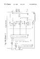
- a modem 100includes an analog I/O portion 110 located on a riser card 111 .
- This analog I/O portion(sometimes referred to as a codec) is then interfaced through a digital link 120 (known as AC-97) to the digital controller 130 of the modem.
- the latter digital portionis located directly on a motherboard 131 and generally includes appropriate modem control circuitry, data pumps, and other functional circuits typically associated with those aspects of a modem. These functions can also be performed, for example, by a so-called host signal processing (HSP) embodiment, in which case the AC 97 digital controller (at least for the modem portions anyway) can consist of as little as a very simple bus interface.
- HSPhost signal processing
- Audio Codec 97The preferred implementation for this digital portion is described in another specification published by Intel known as Audio Codec 97. Version 2.1 of this document, published on May 22, 1998, is likewise available for downloading at Intel's corporate web site, and is also hereby incorporated by reference.
- the AC97 digital controllercan include a wide range of capabilities, including multiple digital audio channels, and suitable interfaces to a PCI bus, a digital I 2 S bus, etc.
- the AC 97 link between the digital controller 130 and the analog CODEC 110consists of a five wire, bi-directional, serial TDM format interface.
- the signals supportedinclude the following: RESET (a master hardware reset), BITCLK (12.288 MHz serial data clock), SYNC (48KHz fixed rate sample sync), SDATA_OUT (serial, time division multiplexed input data stream to the PC), and SDATA_IN (serial, time division multiplexed output data stream from the PC).
- RESETa master hardware reset
- BITCLK(12.288 MHz serial data clock
- SYNC48KHz fixed rate sample sync
- SDATA_OUTserial, time division multiplexed input data stream to the PC
- SDATA_INserial, time division multiplexed output data stream from the PC.
- Digital controller 130can also including suitable interfaces for other contemporary expansion busses, such as PCI bus 141 , USB 142 , etc.
- While the A/M Riser specificationis a step in the right direction, it does not provide for functionality that would permit implementation of an xDSL type modem at this time.
- xDSLrequires a much higher bit rate than that provided by the AC97 link (at a 2.2 MHz sampling and 16 bits wide for an ADSL downstream signal, the total bit rate is 35.2 Mb/s, which is much higher than the 12.288 MHz serial clock).
- the AC97 and A/M Riser specificationare limited to supporting at most simple analog type (V. 90 and the like) modems. This is a significant drawback, since xDSL technologies (and especially ADSL) are expected to be in widespread use in a very short time.
- Another object of the present inventionis to provide a DSL modem which is configurable as a motherboard device within a personal computing system, in a manner similar to that only currently possible for voice band type modems;
- a related object of the present inventionis to provide a DSL modem that has analog codec circuitry and digital controller circuitry both tightly coupled to a PC motherboard, in a manner similar to that only current provided for voice band type modems;
- Another object of the present inventionis to provide a DSL interface that can properly handle DSL data rates, DSL control signals, and other xDSL related signal requirements so that it is suitable for linking the analog and digital portions of a DSL modem of the aforementioned type;
- a related object of the present inventionis to provide a DSL interface that is extremely flexible, and can be used in any one of a number of different xDSL technologies, including HDSL, SDSL, ADSL, reduced rate ADSL, etc.;
- Another object of the present inventionis to provide an improved signal protocol for a DSL link, having data/control word formatting and timing specifications especially suited for a DSL data stream;
- a further object of the present inventionis to provide a DSL interface that minimizes the required signal and power pins associated with a standardized specification for analog codec components in a personal computing system, and is therefore cost effective, and can be easily integrated by system vendors;
- Yet a further object of the present inventionis to provide a DSL digital controller and a DSL codec which can utilize the above novel DSL interface;
- An additional object of the present inventionis to provide a personal computer motherboard which is adapted to use the aforementioned DSL modem and DSL interface.
- Another object of the present inventionis to minimize the required logic complexity in order to support all above functions and features.
- An improved digital communications link of the present inventionconnects a digital controller section of an xDSL modem—which is preferably located on a system motherboard of a computing system—to a separate analog section of the xDSL modem which is located at a position substantially free of electronic noise from other electronic components on said motherboard, which could materially affect the operation of such analog section.
- the data path/linkis generally configured in the following manner: (a) a plurality of receive signal lines are set up for transmitting data from a remote site; (b) a plurality of transmit signal lines are designated for receiving data from a remote site; (c) a bit clock signal line is set up for carrying a clock signal, which clock signal is used in connection with communicating the data to and from the remote site.
- the bit clock signal linecan carry any desired clock signal needed according to data transmission requirements of said digital communications link, thus providing a scalable interface that is easily adaptable for use in any number of different motherboard environments.
- An additional word clock signalderived from the bit clock signal, marks the boundary for each sample word received or transmitted on said plurality of receive signal lines and/or plurality of transmit signal lines respectively.
- Another aspect of the present inventionincludes the use of an improved protocol for exchanging operational and/or control information between separated digital and analog sections of an xDSL modem.
- This operational and/or control informationpreferably includes information relating to real time control settings for circuits located within the analog codec, power management, and the like.
- the aforementioned receive and/or transmit signal linescan also be used for carrying control words for use by the xDSL modem, which control words are embedded as part of the normal data stream.
- these control wordspreferably have either a first or second length.
- the control wordhas a start bit, followed by a length indicator bit, and then the set of command bits corresponding to the actual command/data value. Idle bits are transmitted continuously between control words.
- the control wordsare transmitted asynchronously, therefore, in an embedded operations channel (EOC) that has an effective rate equal to the word clock signal.
- EOCembedded operations channel
- the aforementioned linkalso includes provision for setting up a multi-channel data frame.
- two or more data channelscan be set up between the digital controller and analog section, with data transferred through a first channel during a first time period of the multi-channel data frame, and through a second channel during a second time period of the multi-channel data frame.
- the word clock signalcan be adapted to have a different duration for different number of data channels.
- the data channelscan have different transmit and/or receive data rates, so as to accommodate multiple codecs, or unequal receive/transmit data stream bit rates (such as ADSL). Accordingly, the single channel limitation of the prior art can be also be overcome by this capability of the present invention.
- Yet another useful aspect of the present inventionprovides that, due to the unique selection of receive/transmit/clock lines and signal protocols, the same receive and/or transmit signal lines can also be used to support a compatible data interface between the digital controller and an ATM based hardware xDSL modem.
- the data pathcan handle ATM packaged data and clocking information, making it extremely versatile and useful for incorporation within a motherboard application.
- a computer motherboard, DSL digital controller, DSL codec, and DSL modem of the present inventioninclude otherwise conventional hardware (and/or software in an HSP application) and are all implemented with appropriate interface circuitry and control logic necessary to effectuate the above architecture, characteristics and functionality of the aforementioned DSL link.
- FIG. 1Ais a diagram illustrating how an analog portion of a prior art voice band grade modem is mechanically placed in a riser card and electrically connected to a digital portion of such modem integrated into a computer motherboard in a personal computing system
- FIG. 1Bis an electrical block diagram depicting the various signals carried by a prior art digital link for a voice band grade modem integrated as part of a motherboard in a personal computer system;
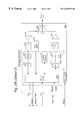
- FIG. 2Ais a functional block diagram of a preferred embodiment of a DSL digital link, DSL modem, and motherboard of the present invention
- FIG. 2Bis a more detailed functional block diagram of the portions of the circuitry illustrated in FIG. 2A;
- FIGS. 3A-3Care preferred embodiments of timing specifications, data formatting, and control signal protocols used in the DSL link of the present invention.
- FIG. 4is a preferred embodiment of a signal and timing protocol that can be used by the DSL link of the present invention to support an ATM interface.
- FIGS. 2A and 2BA preferred embodiment of the present invention is depicted generally in FIGS. 2A and 2B. This embodiment is similar in some respects to the prior art voice band modem implementation shown in FIG. 1, and, for that reason, like components/circuits are designated with like numerals.
- an xDSL modem 200as shown consists of two physically separated (but electrically coupled) circuitry sections, a DSL Modem Analog Circuit 205 , and a DSL Modem Digital Circuit 230 . Except for those portions necessary for implementing the xDSL digital link of the present invention, the specifics of these two circuitry sections are well known in the art, and any suitable hardware/logic/firmware combination could be used for effectuating the typical functions of an xDSL modem.
- DSL Modem Analog Circuit 205is typically a combination of a codec and various analog components necessary to support an xDSL link. It will be apparent to those skilled in the art that portions of DSL Modem Analog Circuit 205 , as well portions (or even all) of DSL Modem Digital Circuit 230 may be implemented in single chip (IC) form either alone or in combination with a larger functional device. With reference to FIG. 2A again, DSL Modem Digital Circuit 230 includes circuitry for performing some of the necessary signal processing associated with an xDSL link, data buffering, and host interface functions. Additional control logic sets up and maintains the xDSL compatible data link by responding to appropriate commands from the host. It also receives hardware status such as power loss detection from the DSL Analog Circuit 205 via the DSL link and passes this information forward to the host for necessary actions.
- DSL Modem Digital Circuit 230can interact with various available system busses such as a PCI Bus to ensure proper data flow between such circuit and applications running on a host system.
- a PCI Busthe functions performed by DSL Modem Digital Circuit 230 is embodied as part of a PCI Bus Controller chipset, such as those known in the art as either South Bridge or North Bridge.
- the purpose of this integrationis to increase system integration flexibility and to reduce BOM costs.
- DSL Modem Digital Circuit 230is also generally referred to herein as a DSL Digital IC, and this IC can be integrated alone as a standalone device, or, as noted immediately above, as part of a PCI North/South Bridge IC.
- this overall chipmay contain additional various interfaces such as a PCI bus 241 , USB bus 242 , and AC-Link 243 . Furthermore, it may generate additional control signals such Wake Up to the host for various modem operation needs.
- PCI Bus Controller chipsetcan be implemented in any conventional, well-known fashion.
- DSL Modem Digital Circuit 230is dependent on the functions performed in DSL Modem Analogy Circuit 205 .
- the digital filters for interpolation and decimation filterscan be done on either side of the DSL link. Therefore, for purposes of the present invention, the actual implementation of DSL Modem Digital Circuit 230 and Digital Modem Analog Circuit 205 can be accomplished through a number of variations that are compatible with the teachings herein.
- various signal processing or logic operationscan be effectuated on either side of the link with no loss of performance or flexibility.
- the present inventionspecifies a universal DSL link interface that allows a very flexible implementation for the two blocks and for future DSL technologies.
- FIG. 2Bprovides a more detailed electrical schematic illustration of the components shown generally in FIG. 2 A.
- a DSL Analog Modem Circuit 205is connected to a phone line through a hybrid circuit 207 and processes the received signal through a receive amplifier 209 , filter 211 , A/D 213 , and, in embodiments where filtering is implemented on this side of the modem, a post digital filter 214 .
- a ring detect circuit 212is used to detect a remote wake up signal, which is some pre-designated xDSL signal. This wake up signal is passed on where it used, for example, to re-activate portions of the DSL modem and a host PC incorporating the same.
- a series of transmission counterpart stagesare also shown in FIG.
- DSL Analog Modem Circuit 205including a digital filter 214 ′ (optional as noted above), D/A circuit 213 ′, and a transmit amplifier and driver stage 211 ′, for generating the xDSL analog transmit signal to the phone line through the hybrid.
- DSL Analog Modem Circuit 205Also associated with DSL Analog Modem Circuit 205 is a DSL link interface block DSL-A 216 , which transmits signals in the DSL link to DSL Digital Modem Circuit 230 , and converts received signals in the DSL link to various data and control signals for the internal circuits within DSL Analog Modem Circuit 205 , including control registers 215 .
- DSL-A 216Also inside DSL-A 216 is a clock circuit (not shown) which generates the necessary clocks for internal blocks and external DSL link based on an input from a System Master Clock as shown.
- DSL Analog Modem Circuit 205may be grouped and implemented in single chip form.
- DSL-A codec 218incorporating control registers 215 , DSL-A Interface 216 , digital filters 214 , 214 ′, and A/D 213 and D/A 213 ′ is preferably embodied in a single integrated circuit (IC), and a separate IC is preferably used to embody analog front end sections (i.e. receive/transmit drivers 209 , 209 ′ and receive/transmit filters 211 and 211 ′).
- DSL Modem Analog Circuit 205can be physically placed in a separate printed circuit board (PCB) or riser card 211 . This provides maximum noise isolation from DSL Modem Digital Circuit 230 . This approach is similar to that done in the prior art for analog modems. Note that it is not necessary in all cases that DSL Modem Analog Circuit 205 be placed on a separate riser card 211 , but it is important that such circuitry be isolated in some fashion so that it is substantially free from electronic noise that could impair its performance.
- PCBprinted circuit board
- riser card 211This provides maximum noise isolation from DSL Modem Digital Circuit 230 . This approach is similar to that done in the prior art for analog modems. Note that it is not necessary in all cases that DSL Modem Analog Circuit 205 be placed on a separate riser card 211 , but it is important that such circuitry be isolated in some fashion so that it is substantially free from electronic noise that could impair its performance.
- DSL Modem Analog Circuit 205could conceivably still be mounted on the same motherboard 231 as DSL Modem Digital Circuit 230 , so long as the former is sufficiently isolated from other motherboard noise sources.
- a small isolating enclosure, shielding cage, or even insulative layer coatingsmight be used to protect and shield portions of DSL Modem Analog Circuit 205 from EMI and other noise, and this could result in smaller displacements between the analog and digital sections of an xDSL modem.
- Other appropriate manifestationswill be apparent to those skilled in the art.
- DSL Modem Digital Circuit 230On the other side of DSL Link 220 is DSL Modem Digital Circuit 230 , which includes a counterpart DSL-D Interface 233 .
- DSL Modem Digital Circuit 230is preferably implemented as a single DSL Digital IC integrated within a South/North bridge controller within a PC system. The functions performed by this circuit include I/ 0 transfers between a PC host and DSL Analog Circuit 205 .
- part of the data pump functionscan be done inside Receiver Buffer and Processing 234 and Transmitter Buffer and Processing 234 ′.
- DSL functionssuch as IFFT and FFT can be performed by 234 ′ and 234 , respectively.
- DSL-D Interface 233interacts with and is responsible for coordinating data/control signals on the digital side of DSL Link 220 . As with its counterpart on the analog side, DSL-A Interface 216 , this circuit performs data conversion and control signaling via DSL Link 220 .
- DSL Digital IC 230may also include various bus connections and interfaces. These include PCI Bus 241 and associated PCI Bus Interface 238 to the PC host, USB 242 and USB Interface 238 ′ to external USB devices, and AC-Link 243 and DC 97 Interface 238 ′′ to external audio and analog modem codecs.
- Digital IC 230is but one typical embodiment for use with the present invention in a PC system, and that other variations of the same will be apparent to those skilled in the art. As noted earlier, some of the functions performed in DSL Digital IC 230 can instead be implemented on the analog side, and vice-versa.
- Transmitter Buffer and Processing 234 ′ and Receiver Buffer and Processing 234depend on the specific xDSL implementation. In the case of host signal processing, where the present invention can be used for great benefits, only minimal functions need be performed inside 234 and 234 ′. Instead, most xDSL functions are performed by the host CPU. The degree of integration of such functions by a CPU are, of course, a function of the available MIPs for performing the same.
- a DSL link 220couples DSL Modem Analog Circuit 205 to DSL Digital IC 230 through DSL-A Interface 216 and DSL-D Interface 233 respectively.
- This linkincludes a number of data and control signal lines. Specifically, there are four (4) receive data lines RX 1 -RX 4 ; four (4) transmit data lines TX 1 -TX 4 ; a variable rate bit clock signal (CLOCK); a word clock signal (WORD CLOCK) to show the word boundary for each sample; and a reset signal (RESET) from the DSL Digital IC 230 to reset the DSL Modem Analog Circuit 205 .
- CLOCKvariable rate bit clock signal
- WORD CLOCKword clock signal
- REETreset signal
- Receive data lines RX 1 -RX 4carry digital samples generated by A/D 213 and assembled and transmitted across the link by DSL-A Interface 216 ; DSL-D interface 233 , conversely dis-assembles and passes these samples on for further signal processing.
- the present inventionmakes use of four parallel lines. This comes from a compromise between the single line prior art approach (which minimizes the number of pin assignments but requires a high clocking rate) and a fully parallel approach (which minimizes the clock rates but requires more driving power and a higher pin count).
- This compromise approachhas the following advantages: (1) since xDSL signals are broadband signals, it minimizes clock frequencies and consequently device power consumption, (2) it reduces the total pin count to an acceptable level, (3) it provides an embedded channel for control signaling (explained shortly), and (4) enables various features such as using the same DSL link 220 as a logically equivalent Utopia interface (explained shortly).
- transmit data lines TX 1 -TX 4carry digital samples from DSL Modem Digital Circuit 220 assembled by DSL-D Interface 233 into suitable form where they are then received and dis-assembled by DSL-A Interface 216 and processed by D/A converter 213 ′ in DSL Modem Analog Circuit 205 to generate the analog transmit xDSL signal.
- Signal line RESETis activated when the PC host tries to reset DSL Modem Analog Circuit 205 ; this can occur, for example, when the xDSL modem must be initialized or re-initialized.
- Signal line CLOCKcarries a scalable rate clock signal, f clock generated by the clock generator inside DSL-A 216 , which can be any suitable and well-known conventional clocking circuit.
- f clockFor a given xDSL link of signal frequency bandwidth B, oversampling factor P, up to 15 bits per sample, f clock is given by:
- a sample wordconsists of 16 bits: 1 control bit and up to 15 sample bits. Therefore, the period of the signal line WORD CLOCK consists of four (4) serial clock periods. That is,
- the clock signal rates for CLOCK and WORD CLOCKwill vary depending on the particular DSL link in place.
- the present DSL Digital Communication Link 220does not impose any restriction on the clock rate, since it is expected that such should be scalable in a manner that supports a wide range of potential options for an xDSL modem in a personal computing system.
- this variability for the clock rateprovides system motherboard manufacturers with the ability to mix and match compatible combinations of digital and analog xDSL modem components without concern about the available clocking rate across the connecting interface. This optimizes options for both motherboard suppliers, and xDSL modem component vendors, since they only need to ensure that they are matching combinations of hardware that are otherwise compatible.
- Pbeing 4X oversampling
- CLOCK and WORD CLOCKare 35.328 and 8.832 MHz, respectively.
- DSL Digital Communications Link 220supports a scalable clock rate that is based purely on the desired price and performance objectives of a system vendor.
- the external Master clockcan be divided by a programmable value specified in a register inside DSL-A Interface 216 , which can be set up by the host through the control channel embedded in the DSL Link 220 (explained shortly).
- DSL-A 216 and DSL-D 233the same CLOCK and WORD CLOCK are used by the corresponding interfaces (DSL-A 216 and DSL-D 233 ) for both transmit and receive data.
- the word clock rate, f wcprovides timing for transmit and receive data samples.
- each pulse in the WORD CLOCKrepresents the beginning of a sample word.
- four sampling CLOCKsare used in a word period. This allows up to 16 bits (4 lines*4 cycles) per sample word, In a typical DSL application, a high speed codec will not require more than 15 bits per sample. Accordingly, the present scheme accommodates even the expected worst case for an xDSL modem by setting 16 bits per WORD CLOCK period, in which at least one of these bits can be designated for control signaling.
- the present inventionalso provides capability for communicating operational and/or control information easily and flexibly between the analog and digital sections of modem 200 .
- FIG. 3Billustrates how at least one operational control bit (D 15 ) is reserved or allocated for an embedded operation channel (EOC).
- EOCembedded operation channel
- the EOCcan be used, for example, for passing the following types of information across the link.
- power management informationsuch as an ADSL wake-up signal, or a power loss signal received by DSL Digital IC 230 from the motherboard.
- the power loss signal from the motherboardin the case of ADSL, is used by DSL Modem Digital Controller 230 for generating a dying gasp message to be transmitted to a remote transceiver through DSL Modem Analog Circuit 205 .
- Other types of control information associated with a conventional xDSL linkcan also be accommodated.
- EOChas an effective bit rate equal to the word clock.
- the present inventiontherefore, provides a method for providing control signaling information that does not require a separate time division multiplexed control word sent over the link as is done in the aforementioned AC97 prior art data link.
- This operational informationis encoded by DSL-D Interface 233 into the data stream using any suitable logic, and is then decoded and acted upon by corresponding logic in DSL-A Interface 216 so that, for example, suitable adjustments are made to digital filters 214 , 214 ′, A/D 213 , D/A 213 ′, and amplifier and filter stages 209 , 209 ′ and 211 , 211 ′ respectively.
- This operational informationcan be passed in both directions across the link so that control registers 215 within DSL Analog Circuit 205 can be read or configured in any desired manner by DSL Digital IC 230 . Conversely, if desired, information concerning data and settings of control registers 235 within DSL Digital IC can be monitored and changed by control logic in DSL Analog Circuit 205 .
- control informationi.e., control data or control data addressing
- control datai.e., control data or control data addressing
- a start bitis set to logical 0 when there is control data, and logical 1 otherwise.
- a fixed number (1+N c or 1+2 N c ) of control bitsfills out the remainder of the control word signal.
- two different control word lengthsare provided (i.e., the control word length is either N c or 2N c ).
- Another useful aspect of the present inventionis the provision in the present xDSL digital link for a variable number of channels.
- the aforementioned AC97 prior artcan only handle a fixed number of channels (12) in the transmit/receive directions, and this is not practical for an xDSL link for a number of reasons.
- the receiving and transmitting data streamsmay not be operating at the same sampling clock. This will occur, for example, when there are different oversampling ratios, or where there are different signal bandwidths (e.g., ADSL) for upstream and downstream transmissions.
- FIG. 3 Ca frame structure for the word clock cycles is illustrated in FIG. 3 C.
- a certain number M(programmable by software and set to a value of 2 as shown) of word clock cycles forms a frame clock to support M separate DSL channels (or separate analog circuits) in each direction. It is unnecessary, of course, for all M channels to be active at one time.
- Mis initially set to 1.
- a multi-channel frameis then indicated by WORD CLOCK being set high for two clock cycles.
- the data for channel 2(or the second DSL Modem analog circuit) is presented at the beginning of the frame cycle (i.e., when WORD CLOCK is high for two cycles) and the data for channel 1 (or the first DSL Modem analog circuit) is presented during the second half of the frame cycle (during the time WORD CLOCK is high for a single cycle).
- DSL Modem Analog Circuits 205multiple codecs can be included in DSL Modem Analog Circuits 205 .
- the value for Mcan be programmed as necessary by DSL Digital IC 230 based on the particular DSL link requirements, the specific implementation of DSL Modem Analog Circuits 205 , etc.
- DSL Link 220is most attractive to a host based DSL modem implementation requiring minimal logic inside Digital IC 230 .
- the CPU in the motherboardis not fast enough, it is desirable to use the DSL Link to connect Digital IC 230 to an external hardware DSL implementation.
- FIG. 4another useful aspect of the present invention is illustrated in FIG. 4 .
- a reasonable interface to use with such implementationis one based on the ATM Utopia I or Utopia II interface. This is because ADSL technology has already been defined to interface with ATM in both T 1 .413 Issue 2 and ITU-T G.992 standards.
- DSL Digital IC 230would be linked through DSL Digital Link 220 to a hardware based xDSL modem in FIG. 2A and 2B, instead of interfacing directly to DSL Analog Modem Circuit 205 .
- DSL Digital Controller 230could be simplified accordingly. The reason this is possible is because the same 10 signal lines described above (RX 1 -RX 4 , TX 1 -TX 4 , CLOCK and WORD CLOCK) can serve a dual purpose and act as an ATM interface as well. As above, for the same four sampling cycles per word clock, the following data can be transported over DSL digital link 220 :
- First clock cycle periodRX 1 -RX 4 are used for Control, 0 , RxClav, TxClav; TX 1 -TX 4 are used for Control, 0 , RxEnb and TxEnb.
- Second clock cycle periodRX 1 -RX 4 are used for RxSoc, RxAddr [2:0], while TX 1 -TX 4 are used for TxSoc, TxAddr [2:0].
- the signals Control, RxClav, TxClav, RxEnb, TxEnb, RxSoc, TxSoc, RxAddr, and TxAddrare defined in the UTOPIA Specification, Level 1 , Version 2.01, published Mar. 21, 1994 by the ATM Forum, and incorporated by reference herein. It can be seen from the above that an ATM type interface can also be implemented by the DSL-A and DSL-D interfaces to exploit the embedded control channel characteristics of the present digital link with great advantage.
- the DSL Digital Link 220can be incorporated within a motherboard of a personal computing system to enable great flexibility in configuring options for an xDSL communications capability.
- a motherboard manufactureror ultimate system vendor
- any particular base level enabled systemto include any desired level of xDSL modem performance and functionality, including either a host based soft modem solution, or a pure hardware type modem solution. This is accomplished by simply stuffing the board with various combinations; for example, a simplified version of DSL Digital Controller 230 can be combined with an ATM based hardware DSP xDSL modem, or, alternatively, a configuration such as shown in FIG. 2B can be implemented for a software modem implementation.
- the flexibility of the data lines of the communications link, and the use of an embedded control channelpermits easy adoption of optimized solutions for any particular application.
- the configuration and selection of the data signal lines, the use of an embedded control channel, the data clocking mechanism, the ability to provide multiple data channels, and the format of control words used in the embedded control channelall contribute to making the present invention easily adaptable and usable with a number of different combinations of digital and analog circuits associated with xDSL modems.
Landscapes
- Engineering & Computer Science (AREA)
- Computer Networks & Wireless Communication (AREA)
- Signal Processing (AREA)
- Communication Control (AREA)
- Telephonic Communication Services (AREA)
Abstract
Description
Claims (77)
Priority Applications (7)
| Application Number | Priority Date | Filing Date | Title |
|---|---|---|---|
| US09/255,235US6345072B1 (en) | 1999-02-22 | 1999-02-22 | Universal DSL link interface between a DSL digital controller and a DSL codec |
| JP2000601756AJP2002538657A (en) | 1999-02-22 | 2000-02-22 | Universal DSL link interface between DSL digital controller and DSL codec |
| EP00908751AEP1169780A1 (en) | 1999-02-22 | 2000-02-22 | Universal dsl link interface between a dsl digital controller and a dsl codec |
| PCT/US2000/004430WO2000051255A1 (en) | 1999-02-22 | 2000-02-22 | Universal dsl link interface between a dsl digital controller and a dsl codec |
| US10/054,294US6804292B2 (en) | 1999-02-22 | 2001-11-13 | Broadband I/O circuits, interface and bus |
| US10/054,410US6836510B2 (en) | 1999-02-22 | 2001-11-13 | DSL link with scaleable performance |
| US10/054,327US6904083B2 (en) | 1999-02-22 | 2001-11-13 | DSL link with embedded control and multi-channel capability |
Applications Claiming Priority (1)
| Application Number | Priority Date | Filing Date | Title |
|---|---|---|---|
| US09/255,235US6345072B1 (en) | 1999-02-22 | 1999-02-22 | Universal DSL link interface between a DSL digital controller and a DSL codec |
Related Child Applications (3)
| Application Number | Title | Priority Date | Filing Date |
|---|---|---|---|
| US10/054,410ContinuationUS6836510B2 (en) | 1999-02-22 | 2001-11-13 | DSL link with scaleable performance |
| US10/054,294ContinuationUS6804292B2 (en) | 1999-02-22 | 2001-11-13 | Broadband I/O circuits, interface and bus |
| US10/054,327ContinuationUS6904083B2 (en) | 1999-02-22 | 2001-11-13 | DSL link with embedded control and multi-channel capability |
Publications (1)
| Publication Number | Publication Date |
|---|---|
| US6345072B1true US6345072B1 (en) | 2002-02-05 |
Family
ID=22967430
Family Applications (4)
| Application Number | Title | Priority Date | Filing Date |
|---|---|---|---|
| US09/255,235Expired - LifetimeUS6345072B1 (en) | 1999-02-22 | 1999-02-22 | Universal DSL link interface between a DSL digital controller and a DSL codec |
| US10/054,327Expired - LifetimeUS6904083B2 (en) | 1999-02-22 | 2001-11-13 | DSL link with embedded control and multi-channel capability |
| US10/054,410Expired - LifetimeUS6836510B2 (en) | 1999-02-22 | 2001-11-13 | DSL link with scaleable performance |
| US10/054,294Expired - LifetimeUS6804292B2 (en) | 1999-02-22 | 2001-11-13 | Broadband I/O circuits, interface and bus |
Family Applications After (3)
| Application Number | Title | Priority Date | Filing Date |
|---|---|---|---|
| US10/054,327Expired - LifetimeUS6904083B2 (en) | 1999-02-22 | 2001-11-13 | DSL link with embedded control and multi-channel capability |
| US10/054,410Expired - LifetimeUS6836510B2 (en) | 1999-02-22 | 2001-11-13 | DSL link with scaleable performance |
| US10/054,294Expired - LifetimeUS6804292B2 (en) | 1999-02-22 | 2001-11-13 | Broadband I/O circuits, interface and bus |
Country Status (4)
| Country | Link |
|---|---|
| US (4) | US6345072B1 (en) |
| EP (1) | EP1169780A1 (en) |
| JP (1) | JP2002538657A (en) |
| WO (1) | WO2000051255A1 (en) |
Cited By (33)
| Publication number | Priority date | Publication date | Assignee | Title |
|---|---|---|---|---|
| US20020008256A1 (en)* | 2000-03-01 | 2002-01-24 | Ming-Kang Liu | Scaleable architecture for multiple-port, system-on-chip ADSL communications systems |
| WO2002061588A1 (en)* | 2001-01-30 | 2002-08-08 | 3Com Corporation | Method and system for an improved motherboard and riser architecture |
| US20020106013A1 (en)* | 2001-02-06 | 2002-08-08 | Norrell Andrew L. | Loop extender with selectable line termination and equalization |
| US20020106076A1 (en)* | 2001-02-06 | 2002-08-08 | Norrell Andrew L. | Line powered loop extender with communications, control, and diagnostics |
| US20020106012A1 (en)* | 2001-02-06 | 2002-08-08 | Norrell Andrew L. | Loop extender with communications, control, and diagnostics |
| US20020110221A1 (en)* | 2001-02-15 | 2002-08-15 | Norrell Andrew L. | System and method for fault isolation for DSL loop extenders |
| US20020122514A1 (en)* | 2000-10-31 | 2002-09-05 | Agere Systems Guardian Corp. | Method and apparatus for synchronizing data transfer |
| US20020141569A1 (en)* | 2001-01-17 | 2002-10-03 | Norrell Andrew L. | DSL compatible load coil |
| US6490639B1 (en)* | 1998-12-09 | 2002-12-03 | Globespanvirata, Inc. | Peripheral component interconnect (PCI) single channel master direct memory access (DMA) serving two separate channels |
| US20030009614A1 (en)* | 2001-07-09 | 2003-01-09 | International Business Machines Corporation | Method for selecting an expansion device in a computer unit, a circuit board, and a computer |
| US20030035471A1 (en)* | 2000-05-31 | 2003-02-20 | George Pitsoulakis | Modem having flexible architecture for connecting to multiple channel interfaces |
| US20030123486A1 (en)* | 2001-12-31 | 2003-07-03 | Globespanvirata Incorporated | System and method for utilizing power management functionality between DSL peers |
| US20030174735A1 (en)* | 2000-02-10 | 2003-09-18 | Daecke Dirk Martin | Data communication system |
| US20030201499A1 (en)* | 1997-10-28 | 2003-10-30 | Hiroshi Komatsu | Semiconductor device and manufacturing method thereof |
| US20030212735A1 (en)* | 2002-05-13 | 2003-11-13 | Nvidia Corporation | Method and apparatus for providing an integrated network of processors |
| US6728817B1 (en)* | 2001-02-12 | 2004-04-27 | Conexant Systems, Inc. | Integrated packet bus for multiple devices |
| US20040114589A1 (en)* | 2002-12-13 | 2004-06-17 | Alfieri Robert A. | Method and apparatus for performing network processing functions |
| US6760333B1 (en)* | 1999-11-22 | 2004-07-06 | Texas Instruments Incorporated | Hybrid digital subscriber loop and voice-band universal serial bus modem |
| US20040160949A1 (en)* | 2003-02-19 | 2004-08-19 | Kim Yong-Ki | Apparatus and method for transmitting voice data on ADSL subscriber Board |
| US6785340B1 (en)* | 2000-05-25 | 2004-08-31 | Adc Dsl Systems, Inc. | PCM upstream and downstream system for universal digital loop carrier |
| US6801541B1 (en)* | 2000-09-29 | 2004-10-05 | Advanced Micro Devices, Inc. | Method and apparatus for data transmission over an AC-97 protocol link |
| US20040228361A1 (en)* | 1999-12-21 | 2004-11-18 | Intel Corporation | Modular broadband adapter system |
| US20050044253A1 (en)* | 2003-07-25 | 2005-02-24 | Samsung Electronics Co., Ltd. | Modem for xDSL system having EOC command filtering function and method of processing EOC command in the modem |
| US6889280B1 (en)* | 2000-06-30 | 2005-05-03 | Intel Corporation | Motherboard extension features to provide plug and play information |
| US6937616B1 (en)* | 1999-07-21 | 2005-08-30 | Velocity Communication, Inc. | Method and apparatus for providing packet based and distributed xDSL communications |
| US6977958B1 (en) | 2000-02-23 | 2005-12-20 | 2Wire, Inc. | Differentially-driven loop extender |
| US7072385B1 (en) | 2000-02-23 | 2006-07-04 | 2Wire, Inc. | Load coil and DSL repeater including same |
| US7158574B2 (en)* | 2001-01-12 | 2007-01-02 | Silicon Laboratories Inc. | Digital interface in radio-frequency apparatus and associated methods |
| US7190715B1 (en)* | 1999-12-23 | 2007-03-13 | Intel Corporation | Asymmetric digital subscriber loop modem |
| US20100241227A1 (en)* | 2009-03-20 | 2010-09-23 | Euteneuer Charles L | Medical device delivery system and method |
| US7913294B1 (en) | 2003-06-24 | 2011-03-22 | Nvidia Corporation | Network protocol processing for filtering packets |
| US20140006677A1 (en)* | 2012-06-29 | 2014-01-02 | Venkatraman Iyer | Embedded control channel for high speed serial interconnect |
| US11058508B2 (en) | 2017-06-29 | 2021-07-13 | Verb Surgical Inc. | Sterile adapter for a linearly-actuating instrument driver |
Families Citing this family (20)
| Publication number | Priority date | Publication date | Assignee | Title |
|---|---|---|---|---|
| US6611891B1 (en)* | 1998-11-23 | 2003-08-26 | Advanced Micro Devices, Inc. | Computer resource configuration mechanism across a multi-pipe communication link |
| US7697507B2 (en)* | 1999-05-27 | 2010-04-13 | Infineon Technologies Ag | Ethernet transport over a telephone line |
| DE19952303A1 (en)* | 1999-10-29 | 2001-05-10 | Siemens Ag | Circuit arrangement and method for data transmission |
| US6839792B2 (en)* | 2000-12-15 | 2005-01-04 | Innovative Concepts, Inc. | Data modem |
| FR2826216B1 (en)* | 2001-06-18 | 2003-09-12 | Cit Alcatel | DIGITAL SIGNAL TRANSMISSION SYSTEM |
| US6793971B2 (en)* | 2001-12-03 | 2004-09-21 | Cardinal Ig Company | Methods and devices for manufacturing insulating glass units |
| US20040123070A1 (en)* | 2002-12-23 | 2004-06-24 | Shidla Dale J. | Automatic detection of different microprocessor architectures |
| DE10334838B4 (en)* | 2003-07-30 | 2005-06-16 | Infineon Technologies Ag | Transceiver assembly and method for bi-directionally transmitting data over a digital interface in a radio |
| US20060141924A1 (en)* | 2004-12-28 | 2006-06-29 | Stefan Mende | Stand-alone digital radio mondiale receiver device |
| FR2882836B1 (en)* | 2005-03-01 | 2007-06-15 | Valeo Systemes Thermiques | METHOD OF TRANSMITTING DATA FROM TERMINAL-SLAVES TO A MASTER TERMINAL ALONG A COMMUNICATION BUS |
| TWI273423B (en)* | 2005-07-15 | 2007-02-11 | Via Tech Inc | Computer system with multi-port bridge and an operating method of the same |
| GB2444191B (en) | 2005-11-26 | 2008-07-16 | Wolfson Microelectronics Plc | Audio device |
| US7928884B2 (en)* | 2007-01-11 | 2011-04-19 | Siflare, Inc. | Analog-to-digital converter with a balanced output |
| US8365024B2 (en)* | 2010-02-26 | 2013-01-29 | Honeywell International Inc. | High integrity data bus fault detection using multiple signal components |
| US8054208B2 (en)* | 2010-03-30 | 2011-11-08 | Honeywell International Inc. | Re-configurable multipurpose analog interface |
| US8782299B2 (en) | 2010-04-27 | 2014-07-15 | Honeywell International Inc. | Re-configurable multi-purpose digital interface |
| US8390324B2 (en) | 2010-09-20 | 2013-03-05 | Honeywell International Inc. | Universal functionality module |
| DE102010042903A1 (en)* | 2010-10-26 | 2012-04-26 | Robert Bosch Gmbh | Transmission method and system |
| US10225290B2 (en)* | 2016-07-15 | 2019-03-05 | Genband Us Llc | Systems and methods for extending DSP capability of existing computing devices |
| CN109531569B (en)* | 2018-12-05 | 2021-08-31 | 北京爱其科技有限公司 | Robot based on interface supporting interconnection of different electronic parts |
Citations (15)
| Publication number | Priority date | Publication date | Assignee | Title |
|---|---|---|---|---|
| US5297231A (en) | 1992-03-31 | 1994-03-22 | Compaq Computer Corporation | Digital signal processor interface for computer system |
| US5408260A (en)* | 1994-01-11 | 1995-04-18 | Northern Telecom Limited | Customer premises ADSL signal distribution arrangement |
| US5680394A (en)* | 1995-07-11 | 1997-10-21 | Amati Communications Corporation | Time division duplexed high speed data transmission system and method |
| US5724413A (en) | 1993-03-25 | 1998-03-03 | U.S. Robotics, Inc. | Host computer digital signal processing system for communicating over voice-grade telephone channels |
| US5835787A (en) | 1994-07-07 | 1998-11-10 | Lucent Technologies, Inc. | System for bi-directionally transferring a digital signal sample from a CODEC to a particular memory location and a second sample from memory to CODEC |
| US5870046A (en) | 1997-04-22 | 1999-02-09 | Silicon Laboratories Inc. | Analog isolation system with digital communication across a capacitive barrier |
| WO1999018754A1 (en) | 1997-10-02 | 1999-04-15 | Alcatel Usa Sourcing, L.P. | System and method for data bus interface |
| US5931929A (en)* | 1996-12-31 | 1999-08-03 | Compaq Computer Corporation | Modem for connection to a telephone line through a either portable computer connector or a docking station |
| US5960036A (en) | 1996-11-04 | 1999-09-28 | Motorola, Inc. | Apparatus and method for auto-configuring a communication system |
| US5970066A (en) | 1996-12-12 | 1999-10-19 | Paradyne Corporation | Virtual ethernet interface |
| US6016311A (en) | 1997-11-19 | 2000-01-18 | Ensemble Communications, Inc. | Adaptive time division duplexing method and apparatus for dynamic bandwidth allocation within a wireless communication system |
| WO2000019617A2 (en) | 1998-09-30 | 2000-04-06 | Conexant Systems, Inc. | Performing digital subscriber line (dsl) modem communication over an ac link bus |
| WO2000019308A1 (en) | 1998-09-30 | 2000-04-06 | Conexant Systems, Inc. | System and method for performing digital signal processing on an ac link bus |
| US6049531A (en)* | 1997-07-14 | 2000-04-11 | At&T Corp | Real-time multimedia conferencing over an ATM network using an intelligent ATM ADSL modem and ADSL access |
| US6072783A (en) | 1994-09-13 | 2000-06-06 | Square D Company | I/O module for a serial multiplex data system with a programmable communication module selector |
Family Cites Families (20)
| Publication number | Priority date | Publication date | Assignee | Title |
|---|---|---|---|---|
| US4999834A (en)* | 1989-03-20 | 1991-03-12 | International Business Machines Corporation | Communication method and apparatus |
| US5689534A (en)* | 1992-05-12 | 1997-11-18 | Apple Computer, Inc. | Audio functional unit and system and method for configuring the same |
| US5404459A (en)* | 1992-07-21 | 1995-04-04 | Advanced Micro Devices | Serial interface module and method in which the clock is only activated to send a predetermined number of data bits |
| US5475691A (en)* | 1993-11-15 | 1995-12-12 | At&T Corp. | Voice activated date rate change in simultaneous voice and data transmission |
| US5606577A (en)* | 1995-01-26 | 1997-02-25 | Motorola Inc. | Method and apparatus for a DMT transmitter having a data for matter coupled directly to a constellation encoder |
| US5659684A (en) | 1995-02-03 | 1997-08-19 | Isdn Systems Corporation | Methods and apparatus for interconnecting personal computers (PCs) and local area networks (LANs) using packet protocols transmitted over a digital data service (DDS) |
| KR0155818B1 (en)* | 1995-04-29 | 1998-11-16 | 김광호 | Adaptive Power Distribution Method and Apparatus in Multicarrier Transmission System |
| US6055268A (en)* | 1996-05-09 | 2000-04-25 | Texas Instruments Incorporated | Multimode digital modem |
| US5852631A (en) | 1996-06-21 | 1998-12-22 | Paradyne Corporation | System and method for establishing link layer parameters based on physical layer modulation |
| US6310876B1 (en)* | 1997-02-14 | 2001-10-30 | Advanced Micro Devices, Inc. | Method and apparatus for managing bin chains in a memory |
| US6269103B1 (en) | 1997-10-06 | 2001-07-31 | Agere Systems Guardian Corp. | High speed data interface using TDM serial bus |
| US6128317A (en) | 1997-12-22 | 2000-10-03 | Motorola, Inc. | Transmitter and receiver supporting differing speed codecs over single links |
| JP3917290B2 (en)* | 1998-03-19 | 2007-05-23 | 富士通株式会社 | SVC access method in terminating station side equipment |
| DE19827285A1 (en) | 1998-06-19 | 1999-12-23 | Alcatel Sa | Method, server and communication node for establishing fee-optimized communication connections |
| US20010014927A1 (en) | 1998-10-15 | 2001-08-16 | Chang Tsung-Yen Dean | Dual interface card and socket |
| US6145039A (en) | 1998-11-03 | 2000-11-07 | Intel Corporation | Method and apparatus for an improved interface between computer components |
| US6272563B1 (en)* | 1998-11-03 | 2001-08-07 | Intel Corporation | Method and apparatus for communicating routing and attribute information for a transaction between hubs in a computer system |
| US6175884B1 (en) | 1998-11-03 | 2001-01-16 | Intel Corporation | Efficient communication of transaction types using separate and orthogonal attribute fields in packet headers transferred between hubs in a computer system |
| US6493326B1 (en)* | 1998-12-03 | 2002-12-10 | Skyworks Solutions, Inc. | Method and apparatus for saving power during punctured transmission of mobile communications |
| US6256697B1 (en) | 1998-12-30 | 2001-07-03 | Intel Corporation | Method and apparatus for reusing arbitration signals to frame data transfers between hub agents |
- 1999
- 1999-02-22USUS09/255,235patent/US6345072B1/ennot_activeExpired - Lifetime
- 2000
- 2000-02-22WOPCT/US2000/004430patent/WO2000051255A1/ennot_activeApplication Discontinuation
- 2000-02-22JPJP2000601756Apatent/JP2002538657A/ennot_activeWithdrawn
- 2000-02-22EPEP00908751Apatent/EP1169780A1/ennot_activeWithdrawn
- 2001
- 2001-11-13USUS10/054,327patent/US6904083B2/ennot_activeExpired - Lifetime
- 2001-11-13USUS10/054,410patent/US6836510B2/ennot_activeExpired - Lifetime
- 2001-11-13USUS10/054,294patent/US6804292B2/ennot_activeExpired - Lifetime
Patent Citations (15)
| Publication number | Priority date | Publication date | Assignee | Title |
|---|---|---|---|---|
| US5297231A (en) | 1992-03-31 | 1994-03-22 | Compaq Computer Corporation | Digital signal processor interface for computer system |
| US5724413A (en) | 1993-03-25 | 1998-03-03 | U.S. Robotics, Inc. | Host computer digital signal processing system for communicating over voice-grade telephone channels |
| US5408260A (en)* | 1994-01-11 | 1995-04-18 | Northern Telecom Limited | Customer premises ADSL signal distribution arrangement |
| US5835787A (en) | 1994-07-07 | 1998-11-10 | Lucent Technologies, Inc. | System for bi-directionally transferring a digital signal sample from a CODEC to a particular memory location and a second sample from memory to CODEC |
| US6072783A (en) | 1994-09-13 | 2000-06-06 | Square D Company | I/O module for a serial multiplex data system with a programmable communication module selector |
| US5680394A (en)* | 1995-07-11 | 1997-10-21 | Amati Communications Corporation | Time division duplexed high speed data transmission system and method |
| US5960036A (en) | 1996-11-04 | 1999-09-28 | Motorola, Inc. | Apparatus and method for auto-configuring a communication system |
| US5970066A (en) | 1996-12-12 | 1999-10-19 | Paradyne Corporation | Virtual ethernet interface |
| US5931929A (en)* | 1996-12-31 | 1999-08-03 | Compaq Computer Corporation | Modem for connection to a telephone line through a either portable computer connector or a docking station |
| US5870046A (en) | 1997-04-22 | 1999-02-09 | Silicon Laboratories Inc. | Analog isolation system with digital communication across a capacitive barrier |
| US6049531A (en)* | 1997-07-14 | 2000-04-11 | At&T Corp | Real-time multimedia conferencing over an ATM network using an intelligent ATM ADSL modem and ADSL access |
| WO1999018754A1 (en) | 1997-10-02 | 1999-04-15 | Alcatel Usa Sourcing, L.P. | System and method for data bus interface |
| US6016311A (en) | 1997-11-19 | 2000-01-18 | Ensemble Communications, Inc. | Adaptive time division duplexing method and apparatus for dynamic bandwidth allocation within a wireless communication system |
| WO2000019617A2 (en) | 1998-09-30 | 2000-04-06 | Conexant Systems, Inc. | Performing digital subscriber line (dsl) modem communication over an ac link bus |
| WO2000019308A1 (en) | 1998-09-30 | 2000-04-06 | Conexant Systems, Inc. | System and method for performing digital signal processing on an ac link bus |
Non-Patent Citations (3)
| Title |
|---|
| Intel Corporation, Audio/Modem Riser Specification, Sep. 10, 1998, Revision 1.01, pp. 1-24. |
| Intel Corporation, Excerpts from Audio Codec '97, May 22, 1998, Revision 2.1, pp. 12-17; p. 22; pp. 26-30; pp. 32-35; pp. 47-48; pp. 56-78. |
| The ATM Forum Technical Committee, UTOPIA Specification Level 1, Version 2.01, pp. 1-15. |
Cited By (53)
| Publication number | Priority date | Publication date | Assignee | Title |
|---|---|---|---|---|
| US20030201499A1 (en)* | 1997-10-28 | 2003-10-30 | Hiroshi Komatsu | Semiconductor device and manufacturing method thereof |
| US6490639B1 (en)* | 1998-12-09 | 2002-12-03 | Globespanvirata, Inc. | Peripheral component interconnect (PCI) single channel master direct memory access (DMA) serving two separate channels |
| US6937616B1 (en)* | 1999-07-21 | 2005-08-30 | Velocity Communication, Inc. | Method and apparatus for providing packet based and distributed xDSL communications |
| US6760333B1 (en)* | 1999-11-22 | 2004-07-06 | Texas Instruments Incorporated | Hybrid digital subscriber loop and voice-band universal serial bus modem |
| US7200156B2 (en)* | 1999-12-21 | 2007-04-03 | Skarpness Mark L | Modular broadband adapter system |
| US20040228361A1 (en)* | 1999-12-21 | 2004-11-18 | Intel Corporation | Modular broadband adapter system |
| US7190715B1 (en)* | 1999-12-23 | 2007-03-13 | Intel Corporation | Asymmetric digital subscriber loop modem |
| US20030174735A1 (en)* | 2000-02-10 | 2003-09-18 | Daecke Dirk Martin | Data communication system |
| US7852884B2 (en)* | 2000-02-10 | 2010-12-14 | Lantiq Deutschland Gmbh | Device and method for multiplexing data in a communication system |
| US6977958B1 (en) | 2000-02-23 | 2005-12-20 | 2Wire, Inc. | Differentially-driven loop extender |
| US7072385B1 (en) | 2000-02-23 | 2006-07-04 | 2Wire, Inc. | Load coil and DSL repeater including same |
| US7075941B2 (en)* | 2000-03-01 | 2006-07-11 | Real Communications, Inc. | Scaleable architecture for multiple-port, system-on-chip ADSL communications systems |
| US20020008256A1 (en)* | 2000-03-01 | 2002-01-24 | Ming-Kang Liu | Scaleable architecture for multiple-port, system-on-chip ADSL communications systems |
| US20060203843A1 (en)* | 2000-03-01 | 2006-09-14 | Realtek Semiconductor Corp. | xDSL function ASIC processor & method of operation |
| US7295571B2 (en) | 2000-03-01 | 2007-11-13 | Realtek Semiconductor Corp. | xDSL function ASIC processor and method of operation |
| US6785340B1 (en)* | 2000-05-25 | 2004-08-31 | Adc Dsl Systems, Inc. | PCM upstream and downstream system for universal digital loop carrier |
| US20030035471A1 (en)* | 2000-05-31 | 2003-02-20 | George Pitsoulakis | Modem having flexible architecture for connecting to multiple channel interfaces |
| US7092375B2 (en)* | 2000-05-31 | 2006-08-15 | Westell Technologies, Inc. | Modem having flexible architecture for connecting to multiple channel interfaces |
| US6889280B1 (en)* | 2000-06-30 | 2005-05-03 | Intel Corporation | Motherboard extension features to provide plug and play information |
| US6801541B1 (en)* | 2000-09-29 | 2004-10-05 | Advanced Micro Devices, Inc. | Method and apparatus for data transmission over an AC-97 protocol link |
| US7158592B2 (en)* | 2000-10-31 | 2007-01-02 | Agere Systems, Inc. | Method and apparatus for synchronizing data transfer |
| US20020122514A1 (en)* | 2000-10-31 | 2002-09-05 | Agere Systems Guardian Corp. | Method and apparatus for synchronizing data transfer |
| US7158574B2 (en)* | 2001-01-12 | 2007-01-02 | Silicon Laboratories Inc. | Digital interface in radio-frequency apparatus and associated methods |
| US6947529B2 (en) | 2001-01-17 | 2005-09-20 | 2Wire, Inc. | DSL compatible load coil |
| US20020141569A1 (en)* | 2001-01-17 | 2002-10-03 | Norrell Andrew L. | DSL compatible load coil |
| WO2002061588A1 (en)* | 2001-01-30 | 2002-08-08 | 3Com Corporation | Method and system for an improved motherboard and riser architecture |
| US20020106012A1 (en)* | 2001-02-06 | 2002-08-08 | Norrell Andrew L. | Loop extender with communications, control, and diagnostics |
| US7190716B2 (en) | 2001-02-06 | 2007-03-13 | 2Wire, Inc | Line powered loop extender with communications, control, and diagnostics |
| US20020106076A1 (en)* | 2001-02-06 | 2002-08-08 | Norrell Andrew L. | Line powered loop extender with communications, control, and diagnostics |
| US20020106013A1 (en)* | 2001-02-06 | 2002-08-08 | Norrell Andrew L. | Loop extender with selectable line termination and equalization |
| US7483528B2 (en) | 2001-02-06 | 2009-01-27 | 2Wire, Inc. | Loop extender with selectable line termination and equalization |
| US7194023B2 (en) | 2001-02-06 | 2007-03-20 | 2Wire, Inc. | Loop extender with communications, control, and diagnostics |
| US6728817B1 (en)* | 2001-02-12 | 2004-04-27 | Conexant Systems, Inc. | Integrated packet bus for multiple devices |
| US7061857B2 (en) | 2001-02-15 | 2006-06-13 | 2Wire, Inc. | System and method for fault isolation for DSL loop extenders |
| US20020110221A1 (en)* | 2001-02-15 | 2002-08-15 | Norrell Andrew L. | System and method for fault isolation for DSL loop extenders |
| US20030009614A1 (en)* | 2001-07-09 | 2003-01-09 | International Business Machines Corporation | Method for selecting an expansion device in a computer unit, a circuit board, and a computer |
| US20030123486A1 (en)* | 2001-12-31 | 2003-07-03 | Globespanvirata Incorporated | System and method for utilizing power management functionality between DSL peers |
| US20080071926A1 (en)* | 2002-05-13 | 2008-03-20 | Hicok Gary D | Method And Apparatus For Providing An Integrated Network Of Processors |
| GB2405244A (en)* | 2002-05-13 | 2005-02-23 | Nvidia Corp | Method and apparatus for providing an integrated network of processors |
| US7620738B2 (en) | 2002-05-13 | 2009-11-17 | Nvidia Corporation | Method and apparatus for providing an integrated network of processors |
| WO2003096202A1 (en)* | 2002-05-13 | 2003-11-20 | Nvidia Corporation | Method and apparatus for providing an integrated network of processors |
| US20030212735A1 (en)* | 2002-05-13 | 2003-11-13 | Nvidia Corporation | Method and apparatus for providing an integrated network of processors |
| GB2405244B (en)* | 2002-05-13 | 2006-01-04 | Nvidia Corp | Method and apparatus for providing an integrated network of processors |
| US7383352B2 (en) | 2002-05-13 | 2008-06-03 | Nvidia Corporation | Method and apparatus for providing an integrated network of processors |
| US7397797B2 (en) | 2002-12-13 | 2008-07-08 | Nvidia Corporation | Method and apparatus for performing network processing functions |
| US20040114589A1 (en)* | 2002-12-13 | 2004-06-17 | Alfieri Robert A. | Method and apparatus for performing network processing functions |
| US20040160949A1 (en)* | 2003-02-19 | 2004-08-19 | Kim Yong-Ki | Apparatus and method for transmitting voice data on ADSL subscriber Board |
| US7913294B1 (en) | 2003-06-24 | 2011-03-22 | Nvidia Corporation | Network protocol processing for filtering packets |
| US20050044253A1 (en)* | 2003-07-25 | 2005-02-24 | Samsung Electronics Co., Ltd. | Modem for xDSL system having EOC command filtering function and method of processing EOC command in the modem |
| US20100241227A1 (en)* | 2009-03-20 | 2010-09-23 | Euteneuer Charles L | Medical device delivery system and method |
| US20140006677A1 (en)* | 2012-06-29 | 2014-01-02 | Venkatraman Iyer | Embedded control channel for high speed serial interconnect |
| US9229897B2 (en)* | 2012-06-29 | 2016-01-05 | Intel Corporation | Embedded control channel for high speed serial interconnect |
| US11058508B2 (en) | 2017-06-29 | 2021-07-13 | Verb Surgical Inc. | Sterile adapter for a linearly-actuating instrument driver |
Also Published As
| Publication number | Publication date |
|---|---|
| US6836510B2 (en) | 2004-12-28 |
| US6904083B2 (en) | 2005-06-07 |
| US20020080869A1 (en) | 2002-06-27 |
| WO2000051255A1 (en) | 2000-08-31 |
| EP1169780A1 (en) | 2002-01-09 |
| US20020064222A1 (en) | 2002-05-30 |
| US6804292B2 (en) | 2004-10-12 |
| US20020061061A1 (en) | 2002-05-23 |
| JP2002538657A (en) | 2002-11-12 |
Similar Documents
| Publication | Publication Date | Title |
|---|---|---|
| US6345072B1 (en) | Universal DSL link interface between a DSL digital controller and a DSL codec | |
| US5708663A (en) | ISDN terminal adapter for use with external modem and employing software-based serial communication framing for ISDN `D` channel signaling | |
| US6240166B1 (en) | LAN connection using analog modems via telephone wiring | |
| US5771232A (en) | Expandable local inter-system bus architecture in a multiplexed environment | |
| US6404780B1 (en) | Synchronizing data transfer protocol across high voltage interface | |
| US5564061A (en) | Reconfigurable architecture for multi-protocol data communications having selection means and a plurality of register sets | |
| JP2000101670A (en) | Interface unit for communication device | |
| US6466584B1 (en) | System and method for performing digital subscriber line (DSL) modem communication over an AC link bus | |
| US6707822B1 (en) | Multi-session asymmetric digital subscriber line buffering and scheduling apparatus and method | |
| KR100807344B1 (en) | Method and apparatus for data transmission via the AC-97 protocol link | |
| US6714590B1 (en) | Integrated modem and line-isolation circuitry and associated method | |
| Stevens | DSPs in communications | |
| US7020187B1 (en) | Integrated modem and line-isolation circuitry with HDLC framing and associated method | |
| US6434634B1 (en) | Method and apparatus adaptable to a standard game port of a personal computer for interfacing an external HSP modem, a joystick and a MIDI interface | |
| US6851003B1 (en) | Integrated packet bus with enhanced bandwidth | |
| US6826225B1 (en) | Integrated modem and line-isolation circuitry with selective raw data or modem data communication and associated method | |
| US7190715B1 (en) | Asymmetric digital subscriber loop modem | |
| US7680069B2 (en) | PCM type interface | |
| Chishtie et al. | A flexible chipset architecture for client-side ADSL modems | |
| JP3148765B2 (en) | Communication cable for matching baud rates between interfaces of different standards | |
| CN1194516A (en) | Circuits for Synthesizing Multiple Pulse Code Modulation Data | |
| WO1997030540A1 (en) | Apparatus and method for protocol interface | |
| JPH07107087A (en) | Ultra-small ISDN communication card | |
| JPH09149144A (en) | Communication equipment and modem core circuit board | |
| JPH10112763A (en) | Line connection device |
Legal Events
| Date | Code | Title | Description |
|---|---|---|---|
| AS | Assignment | Owner name:INTEGRATED TELECOM EXPRESS, INC., CALIFORNIA Free format text:ASSIGNMENT OF ASSIGNORS INTEREST;ASSIGNORS:LIU, MING-KANG;YOUNG, WHU-MING;REEL/FRAME:009858/0751 Effective date:19990301 | |
| STCF | Information on status: patent grant | Free format text:PATENTED CASE | |
| AS | Assignment | Owner name:PCTEL, INC., ILLINOIS Free format text:ASSIGNMENT OF ASSIGNORS INTEREST;ASSIGNOR:INTEGRATED TELECOM EXPRESS, INC.;REEL/FRAME:014718/0139 Effective date:20030514 | |
| FPAY | Fee payment | Year of fee payment:4 | |
| AS | Assignment | Owner name:CONEXANT SYSTEMS, INC., CALIFORNIA Free format text:ASSIGNMENT OF ASSIGNORS INTEREST;ASSIGNOR:PCTEL, INC.;REEL/FRAME:016745/0977 Effective date:20050825 | |
| AS | Assignment | Owner name:BANK OF NEW YORK TRUST COMPANY, N.A., THE,ILLINOIS Free format text:SECURITY AGREEMENT;ASSIGNOR:BROOKTREE BROADBAND HOLDING, INC.;REEL/FRAME:018573/0337 Effective date:20061113 Owner name:BANK OF NEW YORK TRUST COMPANY, N.A., THE, ILLINOI Free format text:SECURITY AGREEMENT;ASSIGNOR:BROOKTREE BROADBAND HOLDING, INC.;REEL/FRAME:018573/0337 Effective date:20061113 | |
| AS | Assignment | Owner name:THE BANK OF NEW YORK TRUST COMPANY, N.A., AS COLLA Free format text:SECURITY AGREEMENT;ASSIGNOR:CONEXANT SYSTEMS, INC.;REEL/FRAME:018855/0035 Effective date:20061113 | |
| FPAY | Fee payment | Year of fee payment:8 | |
| AS | Assignment | Owner name:CONEXANT SYSTEMS, INC., CALIFORNIA Free format text:RELEASE BY SECURED PARTY;ASSIGNOR:THE BANK OF NEW YORK MELLON TRUST COMPANY, N.A.;REEL/FRAME:023134/0285 Effective date:20090821 Owner name:BROOKTREE BROADBAND HOLDING, INC, CALIFORNIA Free format text:RELEASE BY SECURED PARTY;ASSIGNOR:THE BANK OF NEW YORK MELLON TRUST COMPANY, N.A.;REEL/FRAME:023134/0285 Effective date:20090821 Owner name:CONEXANT SYSTEMS, INC.,CALIFORNIA Free format text:RELEASE BY SECURED PARTY;ASSIGNOR:THE BANK OF NEW YORK MELLON TRUST COMPANY, N.A.;REEL/FRAME:023134/0285 Effective date:20090821 Owner name:BROOKTREE BROADBAND HOLDING, INC,CALIFORNIA Free format text:RELEASE BY SECURED PARTY;ASSIGNOR:THE BANK OF NEW YORK MELLON TRUST COMPANY, N.A.;REEL/FRAME:023134/0285 Effective date:20090821 | |
| AS | Assignment | Owner name:IKANOS COMMUNICATIONS, INC., CALIFORNIA Free format text:ASSIGNMENT OF ASSIGNORS INTEREST;ASSIGNORS:CONEXANT SYSTEMS, INC.;CONEXANT, INC.;BROOKTREE BROADBAND HOLDING INC.;REEL/FRAME:023163/0723 Effective date:20090824 Owner name:IKANOS COMMUNICATIONS, INC.,CALIFORNIA Free format text:ASSIGNMENT OF ASSIGNORS INTEREST;ASSIGNORS:CONEXANT SYSTEMS, INC.;CONEXANT, INC.;BROOKTREE BROADBAND HOLDING INC.;REEL/FRAME:023163/0723 Effective date:20090824 | |
| FEPP | Fee payment procedure | Free format text:PAYOR NUMBER ASSIGNED (ORIGINAL EVENT CODE: ASPN); ENTITY STATUS OF PATENT OWNER: LARGE ENTITY | |
| FPAY | Fee payment | Year of fee payment:12 | |
| AS | Assignment | Owner name:ALCATEL-LUCENT USA, INC., NEW JERSEY Free format text:NOTICE OF GRANT OF SECURITY INTEREST IN PATENTS;ASSIGNOR:IKANOS COMMUNICATIONS, INC.;REEL/FRAME:035581/0710 Effective date:20150430 | |
| AS | Assignment | Owner name:SILICON VALLEY BANK, CALIFORNIA Free format text:SECURITY INTEREST;ASSIGNOR:IKANOS COMMUNICATIONS, INC.;REEL/FRAME:035874/0351 Effective date:20150602 | |
| AS | Assignment | Owner name:IKANOS COMMUNICATIONS, INC., CALIFORNIA Free format text:RELEASE BY SECURED PARTY;ASSIGNOR:SILICON VALLEY BANK;REEL/FRAME:036733/0031 Effective date:20150930 Owner name:IKANOS COMMUNICATIONS, INC., CALIFORNIA Free format text:RELEASE BY SECURED PARTY;ASSIGNOR:ALCATEL-LUCENT USA, INC.;REEL/FRAME:036732/0876 Effective date:20150929 | |
| FEPP | Fee payment procedure | Free format text:PAYER NUMBER DE-ASSIGNED (ORIGINAL EVENT CODE: RMPN); ENTITY STATUS OF PATENT OWNER: LARGE ENTITY Free format text:PAYOR NUMBER ASSIGNED (ORIGINAL EVENT CODE: ASPN); ENTITY STATUS OF PATENT OWNER: LARGE ENTITY |