US6344965B1 - Capacitor using high dielectric constant film for semiconductor memory device and fabrication method therefor - Google Patents
Capacitor using high dielectric constant film for semiconductor memory device and fabrication method thereforDownload PDFInfo
- Publication number
- US6344965B1 US6344965B1US09/369,255US36925599AUS6344965B1US 6344965 B1US6344965 B1US 6344965B1US 36925599 AUS36925599 AUS 36925599AUS 6344965 B1US6344965 B1US 6344965B1
- Authority
- US
- United States
- Prior art keywords
- film
- contact hole
- electrode
- diffusion barrier
- patterned
- Prior art date
- Legal status (The legal status is an assumption and is not a legal conclusion. Google has not performed a legal analysis and makes no representation as to the accuracy of the status listed.)
- Expired - Lifetime
Links
- 239000003990capacitorSubstances0.000titleclaimsabstractdescription70
- 239000004065semiconductorSubstances0.000titleclaimsabstractdescription32
- 238000000034methodMethods0.000titleabstractdescription27
- 238000004519manufacturing processMethods0.000titleabstractdescription6
- 238000009792diffusion processMethods0.000claimsabstractdescription63
- 230000004888barrier functionEffects0.000claimsabstractdescription62
- 238000009413insulationMethods0.000claimsabstractdescription58
- 150000004767nitridesChemical class0.000claimsabstractdescription31
- 239000012535impuritySubstances0.000claimsabstractdescription22
- 239000010410layerSubstances0.000claimsabstractdescription21
- 239000000758substrateSubstances0.000claimsabstractdescription19
- 239000011229interlayerSubstances0.000claimsabstractdescription18
- 239000004020conductorSubstances0.000claimsabstractdescription17
- 229910052697platinumInorganic materials0.000claimsdescription12
- 239000000463materialSubstances0.000claimsdescription7
- 229910052741iridiumInorganic materials0.000claimsdescription5
- 229910052707rutheniumInorganic materials0.000claimsdescription5
- WOCIAKWEIIZHES-UHFFFAOYSA-Nruthenium(iv) oxideChemical compoundO=[Ru]=OWOCIAKWEIIZHES-UHFFFAOYSA-N0.000claimsdescription5
- XUIMIQQOPSSXEZ-UHFFFAOYSA-NSiliconChemical compound[Si]XUIMIQQOPSSXEZ-UHFFFAOYSA-N0.000claimsdescription4
- ATJFFYVFTNAWJD-UHFFFAOYSA-NTinChemical compound[Sn]ATJFFYVFTNAWJD-UHFFFAOYSA-N0.000claimsdescription4
- 239000003989dielectric materialSubstances0.000claimsdescription4
- 229910052710siliconInorganic materials0.000claimsdescription4
- 239000010703siliconSubstances0.000claimsdescription4
- 229910020294Pb(Zr,Ti)O3Inorganic materials0.000claimsdescription3
- HTXDPTMKBJXEOW-UHFFFAOYSA-Niridium(IV) oxideInorganic materialsO=[Ir]=OHTXDPTMKBJXEOW-UHFFFAOYSA-N0.000claimsdescription3
- PBCFLUZVCVVTBY-UHFFFAOYSA-Ntantalum pentoxideInorganic materialsO=[Ta](=O)O[Ta](=O)=OPBCFLUZVCVVTBY-UHFFFAOYSA-N0.000claimsdescription3
- 229910052718tinInorganic materials0.000claims2
- 229910052719titaniumInorganic materials0.000claims2
- 229910009973Ti2O3Inorganic materials0.000claims1
- GQUJEMVIKWQAEH-UHFFFAOYSA-Ntitanium(III) oxideChemical compoundO=[Ti]O[Ti]=OGQUJEMVIKWQAEH-UHFFFAOYSA-N0.000claims1
- 230000008569processEffects0.000abstractdescription18
- 230000015654memoryEffects0.000abstractdescription3
- BASFCYQUMIYNBI-UHFFFAOYSA-NplatinumChemical compound[Pt]BASFCYQUMIYNBI-UHFFFAOYSA-N0.000description21
- 238000010586diagramMethods0.000description5
- 238000005229chemical vapour depositionMethods0.000description4
- 230000003647oxidationEffects0.000description3
- 238000007254oxidation reactionMethods0.000description3
- 230000001590oxidative effectEffects0.000description3
- 229910021420polycrystalline siliconInorganic materials0.000description3
- QVGXLLKOCUKJST-UHFFFAOYSA-Natomic oxygenChemical compound[O]QVGXLLKOCUKJST-UHFFFAOYSA-N0.000description2
- 238000005137deposition processMethods0.000description2
- 229910052760oxygenInorganic materials0.000description2
- 239000001301oxygenSubstances0.000description2
- 238000010420art techniqueMethods0.000description1
- 238000004070electrodepositionMethods0.000description1
- 238000005530etchingMethods0.000description1
- 230000006870functionEffects0.000description1
- 230000004048modificationEffects0.000description1
- 238000012986modificationMethods0.000description1
- 238000003860storageMethods0.000description1
Images


Classifications
- H—ELECTRICITY
- H10—SEMICONDUCTOR DEVICES; ELECTRIC SOLID-STATE DEVICES NOT OTHERWISE PROVIDED FOR
- H10D—INORGANIC ELECTRIC SEMICONDUCTOR DEVICES
- H10D84/00—Integrated devices formed in or on semiconductor substrates that comprise only semiconducting layers, e.g. on Si wafers or on GaAs-on-Si wafers
- H—ELECTRICITY
- H10—SEMICONDUCTOR DEVICES; ELECTRIC SOLID-STATE DEVICES NOT OTHERWISE PROVIDED FOR
- H10D—INORGANIC ELECTRIC SEMICONDUCTOR DEVICES
- H10D1/00—Resistors, capacitors or inductors
- H10D1/01—Manufacture or treatment
- H10D1/041—Manufacture or treatment of capacitors having no potential barriers
- H10D1/042—Manufacture or treatment of capacitors having no potential barriers using deposition processes to form electrode extensions
- H—ELECTRICITY
- H10—SEMICONDUCTOR DEVICES; ELECTRIC SOLID-STATE DEVICES NOT OTHERWISE PROVIDED FOR
- H10D—INORGANIC ELECTRIC SEMICONDUCTOR DEVICES
- H10D1/00—Resistors, capacitors or inductors
- H10D1/60—Capacitors
- H10D1/68—Capacitors having no potential barriers
- H10D1/692—Electrodes
- H10D1/711—Electrodes having non-planar surfaces, e.g. formed by texturisation
- H10D1/716—Electrodes having non-planar surfaces, e.g. formed by texturisation having vertical extensions
- H—ELECTRICITY
- H01—ELECTRIC ELEMENTS
- H01L—SEMICONDUCTOR DEVICES NOT COVERED BY CLASS H10
- H01L21/00—Processes or apparatus adapted for the manufacture or treatment of semiconductor or solid state devices or of parts thereof
- H01L21/70—Manufacture or treatment of devices consisting of a plurality of solid state components formed in or on a common substrate or of parts thereof; Manufacture of integrated circuit devices or of parts thereof
- H01L21/71—Manufacture of specific parts of devices defined in group H01L21/70
- H01L21/768—Applying interconnections to be used for carrying current between separate components within a device comprising conductors and dielectrics
- H01L21/76801—Applying interconnections to be used for carrying current between separate components within a device comprising conductors and dielectrics characterised by the formation and the after-treatment of the dielectrics, e.g. smoothing
- H01L21/76802—Applying interconnections to be used for carrying current between separate components within a device comprising conductors and dielectrics characterised by the formation and the after-treatment of the dielectrics, e.g. smoothing by forming openings in dielectrics
- H01L21/76807—Applying interconnections to be used for carrying current between separate components within a device comprising conductors and dielectrics characterised by the formation and the after-treatment of the dielectrics, e.g. smoothing by forming openings in dielectrics for dual damascene structures
- H01L21/7681—Applying interconnections to be used for carrying current between separate components within a device comprising conductors and dielectrics characterised by the formation and the after-treatment of the dielectrics, e.g. smoothing by forming openings in dielectrics for dual damascene structures involving one or more buried masks
- H—ELECTRICITY
- H10—SEMICONDUCTOR DEVICES; ELECTRIC SOLID-STATE DEVICES NOT OTHERWISE PROVIDED FOR
- H10D—INORGANIC ELECTRIC SEMICONDUCTOR DEVICES
- H10D1/00—Resistors, capacitors or inductors
- H10D1/60—Capacitors
- H10D1/68—Capacitors having no potential barriers
- H10D1/682—Capacitors having no potential barriers having dielectrics comprising perovskite structures
Definitions
- the present inventionrelates to a capacitor for a semiconductor memory device and to a fabrication method thereof.
- a capacitor forming a DRAM memory cellemploys a film including a material having a much higher dielectric constant relative to a silicon-based dielectric material that has been generally used.
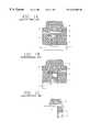
- FIG. 1Ashows an example of a related art capacitor using a film having a high dielectric constant in a semiconductor memory device.
- the related art capacitor as illustrated in FIG. 1Ais fabricated as follows.
- a semiconductor substrate 1has an impurity layer 2 formed at its surface.
- An interlayer insulation film 3is formed on the substrate 1 with a contact hole 4 therethrough exposing the impurity layer 2 .
- the contact hole 4is partially filled with a conductive material.
- a node contact 5is formed to be connected with the conductive material in the contact hole 4 , and is formed of a polycrystalline silicon.
- a diffusion barrier film 6 and a first electrode 7 on the diffusion barrier film 6are formed at a predetermined region on the interlayer insulation film 3 including the node contact 5 .
- a dielectric film 8 having a high dielectric constantis formed on the interlayer insulation film 3 , upper and side portions of the first electrode 7 and side portions of the diffusion barrier film 6 .
- a second electrode 9is formed on the high dielectric constant film 8 to complete fabrication of the capacitor.
- the diffusion barrier film 6prevents the first electrode 7 from reacting with the node contact 5 , which consists of the polycrystalline silicon, while the first electrode 7 is formed of platinum or the like.
- the diffusion barrier film 6prevents oxidation of the node contact 5 in an oxidizing atmosphere while forming the high dielectric constant film 8 . Accordingly, the diffusion barrier film 6 is required to have a superior oxidation resisting property at a high temperature.
- the sidewalls of the diffusion barrier film 6are externally exposed, and thus directly exposed to the oxidizing atmosphere when the high dielectric constant film is formed.
- oxygenis diffused by a distance (d) in from the sidewalls.
- the node contact 5consisting of the polycrystalline silicon is oxidized.
- the diffusion barrier filmmay be formed at the inside of the node contact.
- another related art capacitorhas a diffusion barrier film 6 ′ formed at the inside of a node contact 5 ′.
- a distance (d′) between the sidewall of the first electrode 7 ′ and the diffusion barrier film 6 ′is generally less than 500A, which is similar to the oxygen diffusion distance (d) in the related art capacitor illustrated in FIG. 1 A. As a result, it cannot prevent the node contact 5 ′ from being oxidized.
- FIG. 1Cis a cross-sectional view illustrating an interface of the diffusion barrier film 6 and the node contact 5 when the diffusion barrier film 6 and the first electrode 7 are mis-aligned in the related art capacitor as shown in FIG. 1 A.
- the diffusion barrier 6 and the first electrode 7deviate from a central axis of the node contact 5 and are asymmetrically formed in the related art capacitor as illustrated in FIG. 1 A.
- the node contact 5is externally exposed and the high dielectric constant film 8 is formed thereon, which results in inferior contact and current leakage.
- the above-described related art capacitors using a high dielectric constant film for a semiconductor devicehave various disadvantages.
- An object of the present inventionis to provide a capacitor and method for forming the same that substantially obviates one or more disadvantages of the related art.
- Another object of the present inventionis to provide a capacitor and method for fabricating the same that provides a contact having an increased reliability.
- Another object of the present inventionis to provide a capacitor that increases a process margin for a first electrode position.
- Another object of the present inventionis to provide a capacitor using a high dielectric constant film and method for making the same that provides a contact having an increased reliability and an increased tolerance for electrode positioning.
- a capacitor using a high dielectric constant film for a semiconductor memory devicethat includes a semiconductor substrate having an impurity layer at its surface; an interlayer insulation film formed on the semiconductor substrate and including a contact hole therethrough filled at an inner end portion thereof with a conductive material connected to the impurity layer; a first oxide film formed on an outer portion of 10 the interlayer insulation film; a nitride film formed on an outer portion of the first oxide film; a patterned second oxide film formed on a region of the nitride film; a diffusion barrier film formed on side portions of the second oxide film, outer and side portions of the nitride film where the second oxide film is not formed, side portions of the first oxide film, and an outer end portion of the contact hole; a first electrode formed on the diffusion barrier film; a high dielectric constant film formed on outer portions of the second oxide film, on outer portions of the diffusion barrier film, and on the first electrode; and
- a capacitor for a semiconductor memory devicethat includes a patterned first insulation film that exposes a top surface of a contact hole over a semiconductor substrate, a patterned second insulation film on the patterned first insulation film, a diffusion barrier film on side portions of the second insulation film, side portions of the first insulation film and the top surface of the contact hole, a first electrode on the diffusion barrier film, a dielectric film on outer portions of the second insulation film, outer portions of the diffusion barrier film, and the first electrode, and a second electrode on the dielectric film.
- a method for manufacturing a capacitor according to the present inventionthat includes forming an impurity layer at an outer surface of a semiconductor substrate, forming an interlayer insulation film on the semiconductor substrate having a contact hole therethrough filled with a conductive material, wherein a bottom surface of the conductive material contacts the impurity layer, sequentially forming a first oxide film, a nitride film and a second oxide film on the interlayer insulation film so that a top surface of the conductive material is exposed therethrough, and wherein the nitride film and the first oxide film are partially exposed through the second oxide film, forming a diffusion barrier film at outer and side portions of the second oxide film, side portions of the nitride film, side portions of the first oxide film, and the top surface of the conductive material, forming a first electrode on the diffusion barrier film, removing the diffusion barrier film and the first electrode from an outer portion of the second oxide film, forming a high dielectric constant film on
- FIG. 1Ais a cross-sectional diagram illustrating a related art capacitor for a semiconductor memory device using a high dielectric constant film
- FIG. 1Bis a cross-sectional diagram illustrating another related art capacitor for a semiconductor memory device using a high dielectric constant film
- FIG. 1Cis a cross-sectional view illustrating an interface between a diffusion barrier film and a node contact in the capacitor of FIG. 1A when the diffusion barrier film and first electrode are misaligned;
- FIGS. 2A to 2 Fare diagrams that show cross-sectional views illustrating a preferred embodiment of a process for fabricating a capacitor for a semiconductor memory device in accordance with the present invention.
- FIG. 3is a diagram showing a cross-sectional view of a capacitor formed according to the preferred process of FIGS. 2A-2C when a second oxide film and a first oxide film are mis-aligned.
- a semiconductor substrate 10is formed having an impurity layer 11 preferably formed at its surface and an interlayer insulation film 12 formed thereon.
- a contact hole 13 that exposes the impurity layer 11is provided in the interlayer insulation film 12 .
- the contact hole 13is preferably filled with a conductive material and centered on the impurity layer 11 .
- a first oxide film 14is formed on the interlayer insulation film 12 including over the contact hole 13 by a chemical vapor deposition (CVD) process according to the preferred embodiment for fabricating a capacitor.
- a nitride film 15is formed on the first oxide film 14 , and then a first mask 16 is formed on the nitride film 15 exposing a region of the nitride film 15 that corresponds to the contact hole 13 .
- the exposed region of the nitride film 15 corresponding to the contact hole 13is etched by using the first mask 16 to expose the first oxide film 14 through a hole in the nitride film 15 .
- the size of the hole etched through the nitride film 15preferably defines a width of a node contact 20 a to be formed in a succeeding process.
- a second oxide film 17is formed on the nitride film 15 and on the exposed portion of the first oxide film 14 preferably by a CVD process, a second mask 18 is formed on the second oxide film 17 .
- a center position of a hole of the second mask 18is identical (i.e., aligned over a center position of the contact hole 13 ) to that of the contact hole 13 .
- the hole of the second mask 18is preferably greater in width than the contact hole 13 .
- the size of the hole of the second mask 18preferably defines the width of a first electrode 20 b to be formed in a succeeding process.
- the second oxide film 17 and the first oxide film 14are sequentially etched by using the second mask 18 .
- the nitride film 15is not etched, and the oxide films 14 , 17 are selectively etched.
- an etched region of the second oxide film 17becomes a region for forming the first electrode 20 b .
- the exposed nitride film 15serves as a mask for etching the first oxide film 14 .
- a region of the first oxide film 14is etched more narrowly than the region for the first electrode 20 b .
- the more narrowly etched portion of the first oxide film 14preferably becomes a region for the node contact 20 a.
- a diffusion barrier film 19 of Ti or TiNis formed over the surface of the configuration shown in FIG. 2 C.
- the diffusion barrier 19is on the exposed upper and side portions of the second oxide film 17 , the exposed upper and side portions of the nitride film 15 , the exposed side portions of the first oxide film 14 , and the upper potion of the contact hole 13 .
- the diffusion barrier film 19is formed along the surface of the configuration of FIG. 2C, and preferably has a uniform thickness in order to have an identical surface shape conforming thereto.
- the materials composing the diffusion barrier filmcan further include for example, Ru, Ir and the like, in addition to Ti and TiN.
- a platinum (Pt) film 20is preferably formed on the diffusion barrier film 19 by a CVD process, and a self-aligning process of forming the node contact 20 a and the first electrode 20 b at the same time is completed.
- the platinum film 20is formed along the surface of the diffusion barrier film 19 .
- a portion of the platinum film 20 in the hole formed in the first oxide film 14operates as the node contact 20 a
- the other portion of the platinum film 20 in the hole formed in the second oxide film 17operates as the first electrode 20 b . Accordingly, the first electrode 20 b and the node contact 20 a are not formed by separate processes.
- the platinum film 20is preferably formed by single deposition process that includes the regions serving as the first electrode 20 b and as the node contact 20 a .
- the self-aligning processpreferably includes the single deposition process.
- the materials composing the node contact 20 a and the first electrode 20 bcan include RuO 2 IrO 2 , Ir and the like, in addition to the platinum film.
- the platinum film 20 and the diffusion barrier film 19 formed over the upper portion of the second oxide film 17are etched by an etchback process to be within the hole of the second oxide layer 17 and to separate the first electrode 20 a from first electrodes of adjacent cells of a memory device.
- the platinum film 20is formed as a single first electrode for a single cell.
- a high dielectric constant film 21preferably formed of BST ((Ba,Sr)T 2 O 3 ) is formed on the upper portions of the second oxide film 17 , the diffusion barrier film 19 and the first electrode 20 b , which are exposed by the etchback process, and over the platinum film 20 .
- the materials forming the high dielectric constant filmcan also include Ta 2 O 5 , PZT (Pb(Zr,Ti)O 3 ) and the like, in addition to the BST. That is, the preferred embodiment for fabricating a capacitor uses materials having a higher dielectric constant than the generally-used silicon-based dielectric materials.
- the preferred embodiment for fabricating a capacitoris completed by forming a second electrode 22 on the high dielectric constant film 21 .
- FIG. 2 Fa preferred embodiment of a capacitor according to the present invention is illustrated by FIG. 2 F.
- the preferred embodiment of a capacitor according to the present inventioncan be formed according to the first preferred embodiment for fabricating a capacitor described above.
- the present inventionis not intended to be so limited.
- FIG. 3is a diagram that shows a cross-sectional view of a partially formed capacitor according to the preferred embodiment for fabricating a capacitor.
- the centering position of the hole in the second mask 18 used in fabricating a capacitor in accordance with the present inventionis offset (e.g., not aligned) from that of the contact hole 13 and misaligned.
- the centering position of the hole in the second mask 18is intended to be aligned with the center of the contact hole 13 in the preferred embodiment for fabricating a capacitor.
- the second oxide film 17 and the first oxide film 14were sequentially etched using a misaligned second mask 18 , and is thus altered relative to the configuration shown in FIG. 2 C.
- the first electrodeis asymmetrically formed.
- the contact hole under the diffusion barrier filmis never exposed.
- a process margin determined in consideration of positioning error of the first electrodeis smaller according to the preferred embodiments of the present invention than in the related art capacitor fabricating process.
- the preferred embodiments of a capacitor and a method of fabricating a capacitor according to the present inventionhave various advantages.
- the diffusion barrier filmis formed at the interface of the contact hole and the node contact, and thus, the node contact and first electrode are formed on the diffusion barrier film. Consequently, the diffusion barrier film is not exposed to an oxidizing atmosphere when the high dielectric constant film is formed. Accordingly, an oxidation resisting property of the diffusion barrier film can be significantly increased.
- the preferred embodimentsovercome the disadvantages of the related art technique such as poor contact and current leakage generated because the node contact under the first electrode and the diffusion barrier film can be exposed when mis-aligned. Further, in the preferred embodiments, a proper margin can be provided despite a positioning (mis-registration) error when the first electrode is mis-aligned. Thus, the process margin is significantly improved.
Landscapes
- Semiconductor Memories (AREA)
Abstract
Description
Claims (21)
Priority Applications (1)
| Application Number | Priority Date | Filing Date | Title |
|---|---|---|---|
| US10/017,896US6645811B2 (en) | 1999-03-16 | 2001-12-18 | Capacitor using high dielectric constant film for semiconductor memory device and fabrication method therefor |
Applications Claiming Priority (2)
| Application Number | Priority Date | Filing Date | Title |
|---|---|---|---|
| KR99-8805 | 1999-03-16 | ||
| KR1019990008805AKR100313506B1 (en) | 1999-03-16 | 1999-03-16 | Capacitor in a semiconductor device using a film having a high dielectric constant and fabrication method thereof |
Related Child Applications (1)
| Application Number | Title | Priority Date | Filing Date |
|---|---|---|---|
| US10/017,896DivisionUS6645811B2 (en) | 1999-03-16 | 2001-12-18 | Capacitor using high dielectric constant film for semiconductor memory device and fabrication method therefor |
Publications (1)
| Publication Number | Publication Date |
|---|---|
| US6344965B1true US6344965B1 (en) | 2002-02-05 |
Family
ID=19576703
Family Applications (2)
| Application Number | Title | Priority Date | Filing Date |
|---|---|---|---|
| US09/369,255Expired - LifetimeUS6344965B1 (en) | 1999-03-16 | 1999-08-06 | Capacitor using high dielectric constant film for semiconductor memory device and fabrication method therefor |
| US10/017,896Expired - Fee RelatedUS6645811B2 (en) | 1999-03-16 | 2001-12-18 | Capacitor using high dielectric constant film for semiconductor memory device and fabrication method therefor |
Family Applications After (1)
| Application Number | Title | Priority Date | Filing Date |
|---|---|---|---|
| US10/017,896Expired - Fee RelatedUS6645811B2 (en) | 1999-03-16 | 2001-12-18 | Capacitor using high dielectric constant film for semiconductor memory device and fabrication method therefor |
Country Status (3)
| Country | Link |
|---|---|
| US (2) | US6344965B1 (en) |
| JP (1) | JP4340823B2 (en) |
| KR (1) | KR100313506B1 (en) |
Cited By (5)
| Publication number | Priority date | Publication date | Assignee | Title |
|---|---|---|---|---|
| US20030075753A1 (en)* | 2001-09-14 | 2003-04-24 | Chung-Ming Chu | Stacked capacitor and method for fabricating the same |
| US6645811B2 (en)* | 1999-03-16 | 2003-11-11 | Hyundai Electronics Industries Co., Ltd. | Capacitor using high dielectric constant film for semiconductor memory device and fabrication method therefor |
| US6844581B2 (en)* | 2000-10-26 | 2005-01-18 | Infineon Technologies Ag | Storage capacitor and associated contact-making structure and a method for fabricating the storage capacitor and the contact-making structure |
| CN1293623C (en)* | 2002-12-30 | 2007-01-03 | 海力士半导体有限公司 | Capacitor and its mfg. process |
| US20190189357A1 (en)* | 2017-12-15 | 2019-06-20 | Micron Technology, Inc. | Methods of Incorporating Leaker Devices into Capacitor Configurations to Reduce Cell Disturb |
Families Citing this family (9)
| Publication number | Priority date | Publication date | Assignee | Title |
|---|---|---|---|---|
| KR100390849B1 (en)* | 2001-06-30 | 2003-07-12 | 주식회사 하이닉스반도체 | Method for fabricating capacitor having hafnium oxide |
| KR100438673B1 (en)* | 2001-12-29 | 2004-07-03 | 주식회사 하이닉스반도체 | Method for fabricating capacitor |
| US6900106B2 (en)* | 2002-03-06 | 2005-05-31 | Micron Technology, Inc. | Methods of forming capacitor constructions |
| KR20040008587A (en)* | 2002-07-19 | 2004-01-31 | 주식회사 하이닉스반도체 | Method of manufacturing capacitor for semiconductor device |
| KR100673895B1 (en) | 2004-06-30 | 2007-01-26 | 주식회사 하이닉스반도체 | Manufacturing method of capacitor |
| KR100712502B1 (en)* | 2004-11-30 | 2007-05-02 | 삼성전자주식회사 | Metal-dielectric film-metal capacitor and manufacturing method thereof |
| KR100668833B1 (en)* | 2004-12-17 | 2007-01-16 | 주식회사 하이닉스반도체 | Capacitor Manufacturing Method of Semiconductor Device |
| JP2008072132A (en)* | 2007-10-05 | 2008-03-27 | Nec Electronics Corp | Semiconductor memory device and manufacturing method thereof |
| CN113272941A (en)* | 2018-12-13 | 2021-08-17 | 超极存储器股份有限公司 | Semiconductor module and method for manufacturing the same |
Citations (8)
| Publication number | Priority date | Publication date | Assignee | Title |
|---|---|---|---|---|
| US5385859A (en) | 1992-07-23 | 1995-01-31 | Nec Corporation | Method for fabricating a semiconductor device having a capacitor with a conductive plug structure in a stacked memory cell |
| US5471418A (en)* | 1992-09-07 | 1995-11-28 | Nec Corporation | Semiconductor memory with stacked-capacitor cells |
| US5506166A (en)* | 1993-04-02 | 1996-04-09 | Micron Technology, Inc. | Method for forming capacitor compatible with high dielectric constant materials having a low contact resistance layer |
| US5604659A (en)* | 1992-09-08 | 1997-02-18 | Texas Instruments Incorporated | Microelectronic device with centered storage capacitor cavity sized less than feature size |
| US5691219A (en)* | 1994-09-17 | 1997-11-25 | Kabushiki Kaisha Toshiba | Method of manufacturing a semiconductor memory device |
| US5793057A (en)* | 1994-08-01 | 1998-08-11 | Texas Instruments Incorporated | Conductive amorphous-nitride barrier layer for high dielectric-constant material electrodes |
| US6078492A (en)* | 1998-04-21 | 2000-06-20 | United Microelectronics Corp. | Structure of a capacitor in a semiconductor device having a self align contact window which has a slanted sidewall |
| US6127734A (en)* | 1995-08-25 | 2000-10-03 | Mitsubishi Denki Kabushiki Kaisha | Semiconductor device comprising a contact hole of varying width thru multiple insulating layers |
Family Cites Families (9)
| Publication number | Priority date | Publication date | Assignee | Title |
|---|---|---|---|---|
| JPH0730077A (en)* | 1993-06-23 | 1995-01-31 | Mitsubishi Electric Corp | Semiconductor device and manufacturing method thereof |
| JP3346994B2 (en)* | 1996-09-13 | 2002-11-18 | 株式会社東芝 | Capacitor and method of manufacturing the same |
| TW359868B (en)* | 1997-08-21 | 1999-06-01 | United Microelectronics Corp | DRAM capacitors and production process therefor |
| US5854119A (en)* | 1998-04-13 | 1998-12-29 | Taiwan Semiconductor Manufacturing Company, Ltd. | Robust method of forming a cylinder capacitor for DRAM circuits |
| US6037213A (en)* | 1998-06-03 | 2000-03-14 | Taiwan Semiconductor Manufacturing Company, Ltd. | Method for making cylinder-shaped capacitors for dynamic random access memory |
| US6346454B1 (en)* | 1999-01-12 | 2002-02-12 | Agere Systems Guardian Corp. | Method of making dual damascene interconnect structure and metal electrode capacitor |
| KR100313506B1 (en)* | 1999-03-16 | 2001-11-07 | 김영환 | Capacitor in a semiconductor device using a film having a high dielectric constant and fabrication method thereof |
| US6136695A (en)* | 1999-08-04 | 2000-10-24 | Taiwan Semiconductor Manufacturing Company | Method for fabricating a self-aligned contact |
| US6228711B1 (en)* | 1999-11-30 | 2001-05-08 | United Microelectronics Corp. | Method of fabricating dynamic random access memory |
- 1999
- 1999-03-16KRKR1019990008805Apatent/KR100313506B1/ennot_activeExpired - Fee Related
- 1999-08-06USUS09/369,255patent/US6344965B1/ennot_activeExpired - Lifetime
- 1999-12-15JPJP35641799Apatent/JP4340823B2/ennot_activeExpired - Fee Related
- 2001
- 2001-12-18USUS10/017,896patent/US6645811B2/ennot_activeExpired - Fee Related
Patent Citations (9)
| Publication number | Priority date | Publication date | Assignee | Title |
|---|---|---|---|---|
| US5385859A (en) | 1992-07-23 | 1995-01-31 | Nec Corporation | Method for fabricating a semiconductor device having a capacitor with a conductive plug structure in a stacked memory cell |
| US5471418A (en)* | 1992-09-07 | 1995-11-28 | Nec Corporation | Semiconductor memory with stacked-capacitor cells |
| US5604659A (en)* | 1992-09-08 | 1997-02-18 | Texas Instruments Incorporated | Microelectronic device with centered storage capacitor cavity sized less than feature size |
| US5506166A (en)* | 1993-04-02 | 1996-04-09 | Micron Technology, Inc. | Method for forming capacitor compatible with high dielectric constant materials having a low contact resistance layer |
| US5793057A (en)* | 1994-08-01 | 1998-08-11 | Texas Instruments Incorporated | Conductive amorphous-nitride barrier layer for high dielectric-constant material electrodes |
| US5691219A (en)* | 1994-09-17 | 1997-11-25 | Kabushiki Kaisha Toshiba | Method of manufacturing a semiconductor memory device |
| US5952687A (en)* | 1994-09-17 | 1999-09-14 | Kabushiki Kaisha Toshiba | Semiconductor memory device having a trench capacitor with lower electrode inside the trench |
| US6127734A (en)* | 1995-08-25 | 2000-10-03 | Mitsubishi Denki Kabushiki Kaisha | Semiconductor device comprising a contact hole of varying width thru multiple insulating layers |
| US6078492A (en)* | 1998-04-21 | 2000-06-20 | United Microelectronics Corp. | Structure of a capacitor in a semiconductor device having a self align contact window which has a slanted sidewall |
Cited By (8)
| Publication number | Priority date | Publication date | Assignee | Title |
|---|---|---|---|---|
| US6645811B2 (en)* | 1999-03-16 | 2003-11-11 | Hyundai Electronics Industries Co., Ltd. | Capacitor using high dielectric constant film for semiconductor memory device and fabrication method therefor |
| US6844581B2 (en)* | 2000-10-26 | 2005-01-18 | Infineon Technologies Ag | Storage capacitor and associated contact-making structure and a method for fabricating the storage capacitor and the contact-making structure |
| US20030075753A1 (en)* | 2001-09-14 | 2003-04-24 | Chung-Ming Chu | Stacked capacitor and method for fabricating the same |
| CN1293623C (en)* | 2002-12-30 | 2007-01-03 | 海力士半导体有限公司 | Capacitor and its mfg. process |
| US20190189357A1 (en)* | 2017-12-15 | 2019-06-20 | Micron Technology, Inc. | Methods of Incorporating Leaker Devices into Capacitor Configurations to Reduce Cell Disturb |
| US10650978B2 (en)* | 2017-12-15 | 2020-05-12 | Micron Technology, Inc. | Methods of incorporating leaker devices into capacitor configurations to reduce cell disturb |
| US11404217B2 (en) | 2017-12-15 | 2022-08-02 | Micron Technology, Inc. | Methods of incorporating leaker devices into capacitor configurations to reduce cell disturb, and capacitor configurations incorporating leaker devices |
| US11676768B2 (en) | 2017-12-15 | 2023-06-13 | Micron Technology, Inc. | Methods of incorporating leaker devices into capacitor configurations to reduce cell disturb, and capacitor configurations incorporating leaker devices |
Also Published As
| Publication number | Publication date |
|---|---|
| KR100313506B1 (en) | 2001-11-07 |
| US6645811B2 (en) | 2003-11-11 |
| US20020089811A1 (en) | 2002-07-11 |
| JP4340823B2 (en) | 2009-10-07 |
| JP2000269454A (en) | 2000-09-29 |
| KR20000060481A (en) | 2000-10-16 |
Similar Documents
| Publication | Publication Date | Title |
|---|---|---|
| US6599806B2 (en) | Method for manufacturing a capacitor of a semiconductor device | |
| KR100289739B1 (en) | Method for manufacturing self-aligned stack capacitor using electroplating method | |
| US6294425B1 (en) | Methods of forming integrated circuit capacitors by electroplating electrodes from seed layers | |
| US6078493A (en) | Fin-shaped capacitor | |
| KR100492435B1 (en) | Sidewall capacitance structure and method | |
| US6518120B2 (en) | Capacitor and method of manufacturing the same | |
| US6559025B2 (en) | Method for manufacturing a capacitor | |
| US6344965B1 (en) | Capacitor using high dielectric constant film for semiconductor memory device and fabrication method therefor | |
| US20040241940A1 (en) | Method for fabricating semiconductor device | |
| US6130124A (en) | Methods of forming capacitor electrodes having reduced susceptibility to oxidation | |
| EP0817259A2 (en) | Thin film capacitor with resistance measuring element | |
| US5742472A (en) | Stacked capacitors for integrated circuit devices and related methods | |
| US6461913B2 (en) | Semiconductor memory device having plug contacted to a capacitor electrode and method for fabricating a capacitor of the semiconductor memory device | |
| US6261849B1 (en) | Method of forming integrated circuit capacitors having recessed oxidation barrier spacers and method of forming same | |
| JP2005136414A (en) | CAPACITOR, SEMICONDUCTOR ELEMENT HAVING SAME, AND METHOD FOR MANUFACTURING SAME | |
| KR20000017627A (en) | Dram having a stacked capacitor and a method for fabricating the same | |
| US6180970B1 (en) | Microelectronic devices including ferroelectric capacitors with lower electrodes extending into contact holes | |
| US7064029B2 (en) | Semiconductor memory device and method of producing the same | |
| US5104821A (en) | Method for fabricating stacked capacitors in a DRAM cell | |
| US6229171B1 (en) | Storage element for semiconductor capacitor | |
| KR100346833B1 (en) | Method for manufacturing capacitor of semiconductor memory device using electroplating method | |
| US6501113B2 (en) | Semiconductor device with capacitor using high dielectric constant film or ferroelectric film | |
| KR100269301B1 (en) | Capacitor for preventing barrier layer from oxidizing and manufacturing method thereof | |
| KR20000023170A (en) | Capacitor arranged on a supporting frame in a semiconductor arrangement and method for producing the same | |
| KR100370169B1 (en) | Method for manufacturing capacitor of semiconductor |
Legal Events
| Date | Code | Title | Description |
|---|---|---|---|
| AS | Assignment | Owner name:LG SEMICON CO., LTD., KOREA, REPUBLIC OF Free format text:ASSIGNMENT OF ASSIGNORS INTEREST;ASSIGNOR:ROH, JAE-SUNG;REEL/FRAME:010161/0564 Effective date:19990716 | |
| AS | Assignment | Owner name:HYUNDAI ELECTRONICS INDUSTRIES CO., LTD., KOREA, R Free format text:MERGER;ASSIGNOR:LG SEMICON CO., LTD.;REEL/FRAME:011014/0462 Effective date:20000621 | |
| FEPP | Fee payment procedure | Free format text:PAYOR NUMBER ASSIGNED (ORIGINAL EVENT CODE: ASPN); ENTITY STATUS OF PATENT OWNER: LARGE ENTITY | |
| STCF | Information on status: patent grant | Free format text:PATENTED CASE | |
| FPAY | Fee payment | Year of fee payment:4 | |
| FPAY | Fee payment | Year of fee payment:8 | |
| FEPP | Fee payment procedure | Free format text:PAYER NUMBER DE-ASSIGNED (ORIGINAL EVENT CODE: RMPN); ENTITY STATUS OF PATENT OWNER: LARGE ENTITY Free format text:PAYOR NUMBER ASSIGNED (ORIGINAL EVENT CODE: ASPN); ENTITY STATUS OF PATENT OWNER: LARGE ENTITY | |
| FPAY | Fee payment | Year of fee payment:12 | |
| AS | Assignment | Owner name:SK HYNIX INC, KOREA, REPUBLIC OF Free format text:CHANGE OF NAME;ASSIGNOR:HYNIX SEMICONDUCTOR, INC.;REEL/FRAME:032421/0496 Effective date:20120413 Owner name:HYNIX SEMICONDUCTOR, INC., KOREA, REPUBLIC OF Free format text:CHANGE OF NAME;ASSIGNOR:HYUNDAI ELECTRONICS INDUSTRIES CO., LTD.;REEL/FRAME:032421/0637 Effective date:20010406 Owner name:INTELLECTUAL DISCOVERY CO., LTD., KOREA, REPUBLIC Free format text:ASSIGNMENT OF ASSIGNORS INTEREST;ASSIGNOR:SK HYNIX INC;REEL/FRAME:032421/0488 Effective date:20140218 |