US6344959B1 - Method for sensing the output voltage of a charge pump circuit without applying a load to the output stage - Google Patents
Method for sensing the output voltage of a charge pump circuit without applying a load to the output stageDownload PDFInfo
- Publication number
- US6344959B1 US6344959B1US09/302,826US30282699AUS6344959B1US 6344959 B1US6344959 B1US 6344959B1US 30282699 AUS30282699 AUS 30282699AUS 6344959 B1US6344959 B1US 6344959B1
- Authority
- US
- United States
- Prior art keywords
- charge pump
- voltage
- capacitor
- output
- switch
- Prior art date
- Legal status (The legal status is an assumption and is not a legal conclusion. Google has not performed a legal analysis and makes no representation as to the accuracy of the status listed.)
- Expired - Lifetime
Links
- 238000000034methodMethods0.000titleclaimsabstractdescription10
- 239000003990capacitorSubstances0.000claimsabstractdescription69
- 238000001514detection methodMethods0.000claimsabstractdescription5
- 238000004891communicationMethods0.000claimsdescription16
- 238000012546transferMethods0.000abstractdescription10
- 230000007704transitionEffects0.000description6
- 238000010586diagramMethods0.000description4
- 230000001351cycling effectEffects0.000description1
- 238000011161developmentMethods0.000description1
- 230000003292diminished effectEffects0.000description1
- 238000011160researchMethods0.000description1
- 230000001360synchronised effectEffects0.000description1
- 230000001960triggered effectEffects0.000description1
Images


Classifications
- H—ELECTRICITY
- H02—GENERATION; CONVERSION OR DISTRIBUTION OF ELECTRIC POWER
- H02M—APPARATUS FOR CONVERSION BETWEEN AC AND AC, BETWEEN AC AND DC, OR BETWEEN DC AND DC, AND FOR USE WITH MAINS OR SIMILAR POWER SUPPLY SYSTEMS; CONVERSION OF DC OR AC INPUT POWER INTO SURGE OUTPUT POWER; CONTROL OR REGULATION THEREOF
- H02M3/00—Conversion of DC power input into DC power output
- H02M3/02—Conversion of DC power input into DC power output without intermediate conversion into AC
- H02M3/04—Conversion of DC power input into DC power output without intermediate conversion into AC by static converters
- H02M3/06—Conversion of DC power input into DC power output without intermediate conversion into AC by static converters using resistors or capacitors, e.g. potential divider
- H02M3/07—Conversion of DC power input into DC power output without intermediate conversion into AC by static converters using resistors or capacitors, e.g. potential divider using capacitors charged and discharged alternately by semiconductor devices with control electrode, e.g. charge pumps
- H02M3/073—Charge pumps of the Schenkel-type
Definitions
- a charge pumpcomprises a series of charge transfer elements, each of which increase the output voltage by a quantity of approximately 1*Vin.
- the chargesare integrated over complete clock cycles.
- a resistive or capacitive voltage divideris provided at the output stage of the charge pump in order to sense the output of the charge pump.
- the resistive or capacitive voltage dividerdraws a certain amount of current, thus reducing the efficiency of the charge pump. It would be desirable to find a measurable quantity in the charge pump which is also related to output current in order to sense the output of the charge pump without applying a load to the output stage thereby improving the efficiency of the charge pump.
- the presently disclosed method and apparatusprovide the sensing of an output voltage of a charge pump without applying a load to the output stage.
- the voltage change which occurs across a capacitor of a stage of the charge pump when the charge pump transfers charge to the next stageis proportional to the difference between the voltage at the output of the charge pump under load, and the voltage which will be developed at the output of the charge pump with no load.
- the charge pump undervoltage detection circuitmeasures the voltage at the high side of the capacitor and compares this measured voltage to a reference voltage.
- the voltage at the high side of the capacitoris below the reference voltage, it can be accurately inferred that the voltage at the output of the charge pump is more than a certain voltage below what the output voltage would be if it was unloaded.
- the amount that the output voltage is below its maximum valueis directly related to the output current. In such a manner the output voltage of the charge pump is sensed without using a resistive or capacitive voltage divider thereby improving the efficiency of the charge pump.
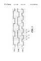
- FIG. 1is a schematic diagram of a prior art charge pump
- FIG. 2is a schematic diagram of a charge pump undervoltage detection circuit of the present invention
- FIG. 3is a timing diagram for the charge pump of FIG. 2;
- FIG. 4is a schematic diagram of the CPUVLO circuitry.
- Voutmax(n+1)*Vin (1)
- a prior art charge pump 1comprises a first driver 20 which drives a first lead of a first capacitor 30 .
- the second lead of the capacitor 30is connected between a first switch 10 and a second switch 40 .
- First switch 10connects Vin to the second lead of capacitor 30 .
- a second driver 50drives a first lead of second capacitor 60 .
- the second lead of capacitor 60is connected between the second switch 40 and a third switch 70 .
- Second switch 40connects between the second end of capacitor 30 and the second lead of capacitor 60 .
- a third switch 70is connected between the second lead of capacitor 60 and to either a reservoir cap or to additional stages (not shown).
- step 1switch 40 is open.
- step 2an input to driver 20 is at a high voltage level, resulting in the output of driver 20 being low.
- step 3the input to driver 50 is set high, thus driver 50 is outputting a low voltage.
- step 10is closed thereby allowing first capacitor 30 to be charged to a value of approximately Vin.
- switch 10is opened.
- the input to driver 20is then set low, resulting in the output of the driver becoming high (approximately five volts).
- the input to driver 50is set high, causing driver 50 to output a low voltage.
- switch 40is then closed which in turn level shifts the voltage at the second lead of capacitor 30 by five volts to approximately ten volts with respect to Vss. This process is repeated such that after several cycles capacitor 60 will be charged to a voltage of approximately twice Vin.
- Switch 70is synchronized with switch 10 , such that switch 70 transfers charge to reservoir capacitor 80 .
- Reservoir capacitor 80provides steady state current to any load on the charge pump.
- a sense resistor 24is shown between the output of the charge pump and the load 90 . The sense resistor 24 senses the load current supplied to the load 90 . The sense resistor 24 draws some amount of current from the charge pump and thus reduces the efficiency of the charge pump.
- FIGS. 2 and 3a charge pump utilizing the presently disclosed method and apparatus is presented.
- CLKAis at a high level
- CLKBis at a low level
- CLKXis toggled from a logic high level to a logic low level.
- switch 110is transitioned from an on state to an off state by the switch having previously supplied approximately 4.0 volts to the VD 0 node.
- Switch 111is off, thereby allowing the VD 0 node to go to approximately 4.0 volts.
- Switch 112is off and switch 113 is on, thereby pulling the VD 1 node to approximately ground level.
- Switch 114is on and switch 130 is off, thus capacitor 120 is charged to approximately 4.0 volts and supplies this voltage to node VC 1 .
- Node VC 1is monitored by the charge pump under voltage detection circuit (CPUVLO). Charge has just been transferred to capacitor 120 , and charge has also been transferred from capacitor 140 to capacitor 160 .
- CPUVLOcharge pump under voltage detection circuit
- CLKBis toggled from a logic low level to a logic high level.
- CLKAremains at a logic high level.
- switch 114is now turning off, which will effectively isolate capacitor 120 from switches 110 and 111 .
- the amount that the output voltage of the charge pump is below its maximum valueis directly related to the output current.
- the voltage change induced on capacitor 120 when it transfers charge to capacitor 140 from T 3 through T 6is a measurable quantity which is also related to output current (Iload).
- Iloadcan be related to packets of charge, q, by:
- each stage of the charge pumpmust transfer charge to the next stage on each clock cycle. If _Vcap is the voltage change across the capacitor from just before to just after the transfer of charge q, then
- the CPUVLO circuitry 101is shown in FIG. 4 .
- the offset voltage 410sets a reference against which ⁇ cap is compared.
- the comparator 420compares the voltage on node VC 1 to the voltage on Vin less the reference voltage 410 .
- the clock signal CKcauses transparent latch 430 to latch the output state of comparator 420 at the time after transferring charge q from capacitor 120 to capacitor 140 , and after closing switch 113 but just prior to closing switch 110 .
- the clock for transparent latch 440is antiphase to the clock for latch 430 .
- Latch 440holds the last latched state of latch 430 during the time when comparator 420 output is settling.
- Transparent latches 430 and 440perform the function of a falling edge triggered D flip flop.
- ⁇ Voutwill be greater than n times the reference voltage 410 , and ⁇ Vc 1 will be greater than the reference voltage 410 .
- the output of the comparator 420will be high, and the CPUVLO output will be high indicating that an undervoltage condition exists. If the charge pump output voltage rises, at the time when ⁇ Vc 1 becomes less than the reference voltage 410 the output of the comparator 420 will become low, and the CPUVLO output will become low indicating that the undervoltage condition no longer exists.
Landscapes
- Engineering & Computer Science (AREA)
- Power Engineering (AREA)
- Dc-Dc Converters (AREA)
Abstract
Description
This application claims priority under 35 U.S.C. § 119(e) to provisional patent application serial No. 60/083,776 filed May 1, 1998; the disclosure of which is incorporated herein by reference.
Not Applicable
Charge pumps are known in the art. A charge pump comprises a series of charge transfer elements, each of which increase the output voltage by a quantity of approximately 1*Vin. The charges are integrated over complete clock cycles. Typically a resistive or capacitive voltage divider is provided at the output stage of the charge pump in order to sense the output of the charge pump. The resistive or capacitive voltage divider draws a certain amount of current, thus reducing the efficiency of the charge pump. It would be desirable to find a measurable quantity in the charge pump which is also related to output current in order to sense the output of the charge pump without applying a load to the output stage thereby improving the efficiency of the charge pump.
The presently disclosed method and apparatus provide the sensing of an output voltage of a charge pump without applying a load to the output stage. In the charge pump the voltage change which occurs across a capacitor of a stage of the charge pump when the charge pump transfers charge to the next stage is proportional to the difference between the voltage at the output of the charge pump under load, and the voltage which will be developed at the output of the charge pump with no load. There is an interval in the timing of the charge pump cycle after the first stage capacitor has transferred its charge to a second stage capacitor where the high side of the first stage capacitor has not yet been connected to the line voltage. During this interval the charge pump undervoltage detection circuit measures the voltage at the high side of the capacitor and compares this measured voltage to a reference voltage. When the voltage at the high side of the capacitor is below the reference voltage, it can be accurately inferred that the voltage at the output of the charge pump is more than a certain voltage below what the output voltage would be if it was unloaded. The amount that the output voltage is below its maximum value is directly related to the output current. In such a manner the output voltage of the charge pump is sensed without using a resistive or capacitive voltage divider thereby improving the efficiency of the charge pump.
The invention will be more fully understood from the following detailed description taken in conjunction with the accompanying drawings in which:
FIG. 1 is a schematic diagram of a prior art charge pump;
FIG. 2 is a schematic diagram of a charge pump undervoltage detection circuit of the present invention;
FIG. 3 is a timing diagram for the charge pump of FIG. 2; and
FIG. 4 is a schematic diagram of the CPUVLO circuitry.
A charge pump comprises a series of charge transfer elements, each increasing the output voltage by a quantity equal to the input voltage (Vin) when integrated over many complete clock cycles. For example, a two stage charge pump having five volts as an input would provide approximately fifteen volts (Vin plus the two stages multiplying Vin). Each charge transfer element adds an equivalent source resistance of 1/(f*C) (where f=oscillator frequency and C=charge pump capacitor values). If there are n stages in the charge pump, the unloaded output voltage will be:
and the output resistance will be:
If there is a steady state output current ILOAD, the output voltage Vout will drop below Voutmax by:
As shown in FIG. 1 a priorart charge pump 1 comprises afirst driver 20 which drives a first lead of afirst capacitor 30. The second lead of thecapacitor 30 is connected between afirst switch 10 and asecond switch 40.First switch 10 connects Vin to the second lead ofcapacitor 30. Asecond driver 50 drives a first lead ofsecond capacitor 60. The second lead ofcapacitor 60 is connected between thesecond switch 40 and athird switch 70.Second switch 40 connects between the second end ofcapacitor 30 and the second lead ofcapacitor 60. Athird switch 70 is connected between the second lead ofcapacitor 60 and to either a reservoir cap or to additional stages (not shown).
Operation of the charge pump can be described as including eight steps. Atstep 1switch 40 is open. In the next step (step2) an input todriver 20 is at a high voltage level, resulting in the output ofdriver 20 being low. In step3 the input todriver 50 is set high, thusdriver 50 is outputting a low voltage.Next switch 10 is closed thereby allowingfirst capacitor 30 to be charged to a value of approximately Vin.
Next, at step5,switch 10 is opened. At step6 the input todriver 20 is then set low, resulting in the output of the driver becoming high (approximately five volts). Next the input todriver 50 is set high, causingdriver 50 to output a low voltage. At step8switch 40 is then closed which in turn level shifts the voltage at the second lead ofcapacitor 30 by five volts to approximately ten volts with respect to Vss. This process is repeated such that afterseveral cycles capacitor 60 will be charged to a voltage of approximately twice Vin.Switch 70 is synchronized withswitch 10, such that switch70 transfers charge toreservoir capacitor 80.Reservoir capacitor 80 provides steady state current to any load on the charge pump. Asense resistor 24 is shown between the output of the charge pump and theload 90. Thesense resistor 24 senses the load current supplied to theload 90. Thesense resistor 24 draws some amount of current from the charge pump and thus reduces the efficiency of the charge pump.
Referring now to FIGS. 2 and 3 a charge pump utilizing the presently disclosed method and apparatus is presented. Initially, at T0, CLKA is at a high level, CLKB is at a low level while CLKX is toggled from a logic high level to a logic low level. As a result of values of CLKA, CLKB and the transition of CLKX,switch 110 is transitioned from an on state to an off state by the switch having previously supplied approximately 4.0 volts to the VD0 node.Switch 111 is off, thereby allowing the VD0 node to go to approximately 4.0 volts.Switch 112 is off and switch113 is on, thereby pulling the VD1 node to approximately ground level.Switch 114 is on andswitch 130 is off, thuscapacitor 120 is charged to approximately 4.0 volts and supplies this voltage to node VC1. Node VC1 is monitored by the charge pump under voltage detection circuit (CPUVLO). Charge has just been transferred tocapacitor 120, and charge has also been transferred fromcapacitor 140 tocapacitor 160.
Thereafter, at T1CLKB is toggled from a logic low level to a logic high level. CLKA remains at a logic high level. As a result of the transition ofCLKB switch 114 is now turning off, which will effectively isolatecapacitor 120 fromswitches
At T2CLKA is transitioned from a logic high level to a logic low level, resulting inswitches capacitor 120 is now in electrical communication withcapacitor 140.
At T3CLKX has transitioned from a logic low level to a logic high level. As a result of the transition of CLKX,switch 112 is closed, level shifting the voltage at node VC1 by approximately four volts, up to approximately 8.0 volts with respect to ground. Node VC2 will also be set to this value by the charging ofcapacitor 140.
At T4, CLKX has transitioned from a logic high level to a logic low level. As a result of the transition of CLKX,switch 112 is opened thereby stopping the transfer of charge fromcapacitor 120 tocapacitor 140.
At T5CLKA is transitioned from a logic low level to a logic high level. As a result of the transition of CLKA,switch 130 is opened, thuscapacitor 120 is no longer in electrical communication withcapacitor 140.Switch 131 is also opened, thus removing the ground path to thecapacitor 140.
At T6CLKB is transitioned from a logic high level to a logic low level. As a result of the transition of CLKB switches114,113 and150 are closed.
During the charge pump cycling described above, there is a timing interval, indicated by T6, wherein charge has been transferred fromcapacitor 120 tocapacitor 140, andcapacitor 120 has not yet been connected to node Vin. During the interval from T6through the time when CLKX rises, the voltage at the top of capacitor120 (VC1) is sensed by theCPUVLO circuitry 101.
The amount that the output voltage of the charge pump is below its maximum value is directly related to the output current. The voltage change induced oncapacitor 120 when it transfers charge tocapacitor 140 from T3through T6is a measurable quantity which is also related to output current (Iload).
Iload can be related to packets of charge, q, by:
therefore:
In the steady state, each stage of the charge pump must transfer charge to the next stage on each clock cycle. If _Vcap is the voltage change across the capacitor from just before to just after the transfer of charge q, then
combining equations (4) & (5):
Prior to transferring charge q fromcapacitor 120 tocapacitor 140, switches110,113, and114 are closed setting the voltage oncapacitor 120 equal to Vin. After transferring charge q fromcapacitor 120 tocapacitor 140, and after closingswitch 113 but prior to closingswitch 110, the voltage oncapacitor 120, and hence the voltage on node VC1, will be Vin−q/c. Thus if the voltage on VC1 at that time is compared to the voltage at Vin, the difference will be equal to ΔVcap=q/c.
TheCPUVLO circuitry 101 is shown in FIG.4. The offsetvoltage 410 sets a reference against which Δcap is compared. Thecomparator 420 compares the voltage on node VC1 to the voltage on Vin less thereference voltage 410. The clock signal CK causestransparent latch 430 to latch the output state ofcomparator 420 at the time after transferring charge q fromcapacitor 120 tocapacitor 140, and after closingswitch 113 but just prior to closingswitch 110. The clock fortransparent latch 440 is antiphase to the clock forlatch 430.Latch 440 holds the last latched state oflatch 430 during the time whencomparator 420 output is settling.Transparent latches
On initial start up of the charge pump, or after a very large current load has diminished the charge pump output voltage, ΔVout will be greater than n times thereference voltage 410, and ΔVc1 will be greater than thereference voltage 410. In this case the output of thecomparator 420 will be high, and the CPUVLO output will be high indicating that an undervoltage condition exists. If the charge pump output voltage rises, at the time when ΔVc1 becomes less than thereference voltage 410 the output of thecomparator 420 will become low, and the CPUVLO output will become low indicating that the undervoltage condition no longer exists.
In such a manner the output voltage of the charge pump has been sensed without applying any load to the charge pump. Since a load is not required to sense the output of the charge pump, the efficiency of the charge pump is improved over a charge pump in which a resistive divider or other load is used to sense the output of the charge pump.
Having described preferred embodiments it will now become apparent to one of ordinary skill in the art that other embodiments incorporating these concepts could also be used. Accordingly, it is submitted that the invention should not be limited to the described embodiments but rather should be limited only by the scope and spirit of the appended claims.
Claims (14)
1. A method of sensing an output voltage of a charge pump without applying a load to an output stage of the charge pump comprising the steps of:
establishing a reference voltage;
sensing with an undervoltage detector a voltage on a first side of a first stage charge pump capacitor related to the output voltage of said charge pump;
comparing the sensed voltage to the reference voltage with said undervoltage detector; and
detecting said undervoltage condition of the charge pump based on the comparison between the sensed voltage and the reference voltage.
2. The method ofclaim 1 wherein the step of sensing is performed after said first stage charge pump capacitor has transferred charge to a second stage charge pump capacitor and before the first side of said first stage charge pump capacitor has been placed in electrical communication with an input voltage.
3. The method ofclaim 1 wherein the step of establishing a reference voltage establishes a reference voltage which has a lower value than an input voltage to said charge pump.
4. A charge pump comprising:
a first capacitor having a first contact and a second contact;
a first device having an input and an output, the output in electrical communication with the first contact of said first capacitor;
a first switch having a source in electrical communication with an input voltage, a drain in electrical communication with said second contact of said first capacitor, and a gate operative to selectively provide electrical communication between said drain and said source;
a second capacitor having a first contact and a second contact;
a second device having an input and an output, the output in electrical communication with the first contact of said second capacitor;
a second switch having a source in electrical communication with the second contact of said first capacitor, a drain in electrical communication with said second contact of said second capacitor, and a gate operative to selectively provide electrical communication between said drain and said source; and
an undervoltage detection circuit in communication with the second contact of said first capacitor.
5. The charge pump ofclaim 4 wherein said first switch comprises a PMOS switch.
6. The charge pump ofclaim 4 wherein said second switch comprises a PMOS switch.
7. The charge pump ofclaim 4 wherein said first device comprises a driver.
8. The charge pump ofclaim 4 wherein said second device comprises a driver.
9. The charge pump ofclaim 4 wherein said first device comprises a switch.
10. The charge pump ofclaim 4 wherein said second device comprises a switch.
11. The charge pump ofclaim 4 wherein said first device comprises a transistor.
12. The charge pump ofclaim 4 wherein said second device comprises a transistor.
13. The method ofclaim 1 further including the steps of,
electrically communicating an output of a first device with a second side of said first stage charge pump capacitor,
selectively providing electrical communication between a drain and a source of a first switch operative by a gate of said first switch when said source is in electrical communication with an input voltage,
electrically communicating an output of a second device with a first side of a second stage charge pump capacitor, and
selectively providing electrical communication between a drain and a source of a second switch operative by a gate of said second switch when said source is in electrical communication with said first side of said first stage charge pump capacitor.
14. The method ofclaim 1 wherein said undervoltage detector detects said undervoltage condition when the sensed voltage is greater than said reference voltage.
Priority Applications (1)
| Application Number | Priority Date | Filing Date | Title |
|---|---|---|---|
| US09/302,826US6344959B1 (en) | 1998-05-01 | 1999-04-30 | Method for sensing the output voltage of a charge pump circuit without applying a load to the output stage |
Applications Claiming Priority (2)
| Application Number | Priority Date | Filing Date | Title |
|---|---|---|---|
| US8377698P | 1998-05-01 | 1998-05-01 | |
| US09/302,826US6344959B1 (en) | 1998-05-01 | 1999-04-30 | Method for sensing the output voltage of a charge pump circuit without applying a load to the output stage |
Publications (1)
| Publication Number | Publication Date |
|---|---|
| US6344959B1true US6344959B1 (en) | 2002-02-05 |
Family
ID=26769732
Family Applications (1)
| Application Number | Title | Priority Date | Filing Date |
|---|---|---|---|
| US09/302,826Expired - LifetimeUS6344959B1 (en) | 1998-05-01 | 1999-04-30 | Method for sensing the output voltage of a charge pump circuit without applying a load to the output stage |
Country Status (1)
| Country | Link |
|---|---|
| US (1) | US6344959B1 (en) |
Cited By (64)
| Publication number | Priority date | Publication date | Assignee | Title |
|---|---|---|---|---|
| US6781422B1 (en) | 2003-09-17 | 2004-08-24 | System General Corp. | Capacitive high-side switch driver for a power converter |
| US6836173B1 (en) | 2003-09-24 | 2004-12-28 | System General Corp. | High-side transistor driver for power converters |
| US20050237679A1 (en)* | 2004-04-26 | 2005-10-27 | Norbert Huber | Protective circuit for a frequency converter |
| US20050280423A1 (en)* | 2004-06-21 | 2005-12-22 | Barbour Erskine R | Method and apparatus for measuring voltage in a power switching device |
| US20070032016A1 (en)* | 2001-11-19 | 2007-02-08 | Saifun Semiconductors Ltd. | Protective layer in memory device and method therefor |
| US20070051982A1 (en)* | 2005-07-18 | 2007-03-08 | Saifun Semiconductors Ltd. | Dense non-volatile memory array and method of fabrication |
| US20070069714A1 (en)* | 2005-09-27 | 2007-03-29 | Saifun Semiconductors, Ltd. | Method for measuring charge pump output current |
| US20070096199A1 (en)* | 2005-09-08 | 2007-05-03 | Eli Lusky | Method of manufacturing symmetric arrays |
| US20070109020A1 (en)* | 2005-11-16 | 2007-05-17 | Ta-Yung Yang | High-side transistor driver having positive feedback for improving speed and power saving |
| US20070120180A1 (en)* | 2005-11-25 | 2007-05-31 | Boaz Eitan | Transition areas for dense memory arrays |
| US20070133276A1 (en)* | 2003-09-16 | 2007-06-14 | Eli Lusky | Operating array cells with matched reference cells |
| US20070159880A1 (en)* | 2006-01-12 | 2007-07-12 | Boaz Eitan | Secondary injection for NROM |
| US20070168637A1 (en)* | 2003-01-31 | 2007-07-19 | Yan Polansky | Memory array programming circuit and a method for using the circuit |
| US20070171717A1 (en)* | 2004-08-12 | 2007-07-26 | Saifun Semiconductors Ltd. | Dynamic matching of signal path and reference path for sensing |
| US20070196982A1 (en)* | 2006-02-21 | 2007-08-23 | Saifun Semiconductors Ltd. | Nrom non-volatile mode of operation |
| US20070195607A1 (en)* | 2006-02-21 | 2007-08-23 | Saifun Semiconductors Ltd. | Nrom non-volatile memory and mode of operation |
| US20070253248A1 (en)* | 2006-04-27 | 2007-11-01 | Eduardo Maayan | Method for programming a reference cell |
| US20070285130A1 (en)* | 2006-06-12 | 2007-12-13 | Pei-Sheng Tsu | Floating driving circuit |
| US20080001195A1 (en)* | 2006-06-28 | 2008-01-03 | System General Corp. | Integrated circuit with high voltage junction structure |
| US7317633B2 (en) | 2004-07-06 | 2008-01-08 | Saifun Semiconductors Ltd | Protection of NROM devices from charge damage |
| US20080036027A1 (en)* | 2006-08-11 | 2008-02-14 | System General Corp. | Integrated circuit for a high-side transistor driver |
| US20080079479A1 (en)* | 2006-09-29 | 2008-04-03 | Micron Technology, Inc. | Reduced time constant charge pump and method for charging a capacitive load |
| US20080094127A1 (en)* | 2006-09-18 | 2008-04-24 | Yoram Betser | Measuring and controlling current consumption and output current of charge pumps |
| US7369440B2 (en) | 2005-01-19 | 2008-05-06 | Saifun Semiconductors Ltd. | Method, circuit and systems for erasing one or more non-volatile memory cells |
| US20080111177A1 (en)* | 1997-08-01 | 2008-05-15 | Eduardo Maayan | Non-volatile memory cell and non-volatile memory device using said cell |
| US20090058506A1 (en)* | 2007-08-28 | 2009-03-05 | Prajit Nandi | Bottom Plate Regulation of Charge Pumps |
| US20090058507A1 (en)* | 2007-08-28 | 2009-03-05 | Prajit Nandi | Bottom Plate Regulated Charge Pump |
| US7532529B2 (en) | 2004-03-29 | 2009-05-12 | Saifun Semiconductors Ltd. | Apparatus and methods for multi-level sensing in a memory array |
| US20090153230A1 (en)* | 2007-12-12 | 2009-06-18 | Feng Pan | Low Voltage Charge Pump with Regulation |
| US20090153231A1 (en)* | 2007-12-12 | 2009-06-18 | Feng Pan | Diode Connected Regulation of Charge Pumps |
| US20090251005A1 (en)* | 2008-04-07 | 2009-10-08 | Liebert Corporation | Undervoltage transfer detection |
| US20090302930A1 (en)* | 2008-06-09 | 2009-12-10 | Feng Pan | Charge Pump with Vt Cancellation Through Parallel Structure |
| US20090315616A1 (en)* | 2008-06-24 | 2009-12-24 | Qui Vi Nguyen | Clock Generator Circuit for a Charge Pump |
| US7638835B2 (en) | 2006-02-28 | 2009-12-29 | Saifun Semiconductors Ltd. | Double density NROM with nitride strips (DDNS) |
| US7675782B2 (en) | 2002-10-29 | 2010-03-09 | Saifun Semiconductors Ltd. | Method, system and circuit for programming a non-volatile memory array |
| US7683700B2 (en) | 2008-06-25 | 2010-03-23 | Sandisk Corporation | Techniques of ripple reduction for charge pumps |
| US20100148856A1 (en)* | 2008-12-17 | 2010-06-17 | Man Lung Lui | Regulation of Recovery Rates in Charge Pumps |
| US20100156513A1 (en)* | 2008-12-23 | 2010-06-24 | Pratt & Whitney Rocketdyne, Inc. | Charge pump |
| US20100173464A1 (en)* | 2004-10-14 | 2010-07-08 | Eli Lusky | Non-volatile memory structure and method of fabrication |
| US20110018615A1 (en)* | 2009-07-21 | 2011-01-27 | Feng Pan | Charge Pump with Current Based Regulation |
| US20110018617A1 (en)* | 2009-07-24 | 2011-01-27 | Khin Htoo | Charge Pump with Reduced Energy Consumption Through Charge Sharing and Clock Boosting Suitable for High Voltage Word Line in Flash Memories |
| US20110133820A1 (en)* | 2009-12-09 | 2011-06-09 | Feng Pan | Multi-Stage Charge Pump with Variable Number of Boosting Stages |
| US20110148509A1 (en)* | 2009-12-17 | 2011-06-23 | Feng Pan | Techniques to Reduce Charge Pump Overshoot |
| US7969235B2 (en) | 2008-06-09 | 2011-06-28 | Sandisk Corporation | Self-adaptive multi-stage charge pump |
| US8294509B2 (en) | 2010-12-20 | 2012-10-23 | Sandisk Technologies Inc. | Charge pump systems with reduction in inefficiencies due to charge sharing between capacitances |
| US8339185B2 (en) | 2010-12-20 | 2012-12-25 | Sandisk 3D Llc | Charge pump system that dynamically selects number of active stages |
| US8400212B1 (en) | 2011-09-22 | 2013-03-19 | Sandisk Technologies Inc. | High voltage charge pump regulation system with fine step adjustment |
| US8514628B2 (en) | 2011-09-22 | 2013-08-20 | Sandisk Technologies Inc. | Dynamic switching approach to reduce area and power consumption of high voltage charge pumps |
| US8699247B2 (en) | 2011-09-09 | 2014-04-15 | Sandisk Technologies Inc. | Charge pump system dynamically reconfigurable for read and program |
| US8710909B2 (en) | 2012-09-14 | 2014-04-29 | Sandisk Technologies Inc. | Circuits for prevention of reverse leakage in Vth-cancellation charge pumps |
| US8836412B2 (en) | 2013-02-11 | 2014-09-16 | Sandisk 3D Llc | Charge pump with a power-controlled clock buffer to reduce power consumption and output voltage ripple |
| US8981835B2 (en) | 2013-06-18 | 2015-03-17 | Sandisk Technologies Inc. | Efficient voltage doubler |
| US9007046B2 (en) | 2013-06-27 | 2015-04-14 | Sandisk Technologies Inc. | Efficient high voltage bias regulation circuit |
| US9024680B2 (en) | 2013-06-24 | 2015-05-05 | Sandisk Technologies Inc. | Efficiency for charge pumps with low supply voltages |
| US9077238B2 (en) | 2013-06-25 | 2015-07-07 | SanDisk Technologies, Inc. | Capacitive regulation of charge pumps without refresh operation interruption |
| US9083231B2 (en) | 2013-09-30 | 2015-07-14 | Sandisk Technologies Inc. | Amplitude modulation for pass gate to improve charge pump efficiency |
| US9154027B2 (en) | 2013-12-09 | 2015-10-06 | Sandisk Technologies Inc. | Dynamic load matching charge pump for reduced current consumption |
| US9491151B2 (en)* | 2015-01-07 | 2016-11-08 | Ememory Technology Inc. | Memory apparatus, charge pump circuit and voltage pumping method thereof |
| US9520776B1 (en) | 2015-09-18 | 2016-12-13 | Sandisk Technologies Llc | Selective body bias for charge pump transfer switches |
| US9647536B2 (en) | 2015-07-28 | 2017-05-09 | Sandisk Technologies Llc | High voltage generation using low voltage devices |
| US9917507B2 (en) | 2015-05-28 | 2018-03-13 | Sandisk Technologies Llc | Dynamic clock period modulation scheme for variable charge pump load currents |
| US9929643B2 (en) | 2016-03-31 | 2018-03-27 | Nxp B.V. | Charge pump circuit and method for operating a charge pump circuit |
| CN110149046A (en)* | 2019-05-27 | 2019-08-20 | 南京芯耐特半导体有限公司 | Relative constant CMOS charge pump is exported based on wide-range input voltage |
| US10985653B1 (en)* | 2020-03-20 | 2021-04-20 | Infineon Technologies Ag | Charge pump converter and control method |
Citations (27)
| Publication number | Priority date | Publication date | Assignee | Title |
|---|---|---|---|---|
| US4291366A (en) | 1979-09-24 | 1981-09-22 | Ncr Corporation | Switching regulated power supply |
| US4670861A (en) | 1985-06-21 | 1987-06-02 | Advanced Micro Devices, Inc. | CMOS N-well bias generator and gating system |
| US4752699A (en)* | 1986-12-19 | 1988-06-21 | International Business Machines Corp. | On chip multiple voltage generation using a charge pump and plural feedback sense circuits |
| US4792705A (en) | 1986-03-14 | 1988-12-20 | Western Digital Corporation | Fast switching charge pump |
| US4870553A (en) | 1988-11-04 | 1989-09-26 | Compaq Computer Corporation | Double-switched flyback power-converter |
| US4883976A (en) | 1987-12-02 | 1989-11-28 | Xicor, Inc. | Low power dual-mode CMOS bias voltage generator |
| US4897774A (en) | 1985-10-01 | 1990-01-30 | Maxim Integrated Products | Integrated dual charge pump power supply and RS-232 transmitter/receiver |
| US4926354A (en) | 1989-09-26 | 1990-05-15 | Allied-Signal Inc. | Power controller with low standby current drain |
| US5039877A (en) | 1990-08-30 | 1991-08-13 | Micron Technology, Inc. | Low current substrate bias generator |
| US5075572A (en) | 1990-05-18 | 1991-12-24 | Texas Instruments Incorporated | Detector and integrated circuit device including charge pump circuits for high load conditions |
| US5119265A (en) | 1990-04-02 | 1992-06-02 | Motorola, Inc. | Semiconductor device protection circuit |
| US5128560A (en) | 1991-03-22 | 1992-07-07 | Micron Technology, Inc. | Boosted supply output driver circuit for driving an all N-channel output stage |
| US5196739A (en) | 1991-04-03 | 1993-03-23 | National Semiconductor Corporation | High voltage charge pump |
| US5301097A (en) | 1992-06-10 | 1994-04-05 | Intel Corporation | Multi-staged charge-pump with staggered clock phases for providing high current capability |
| US5363333A (en) | 1992-09-30 | 1994-11-08 | Nec Corporation | Dynamic random access memory device having power supply system appropriately biasing switching transistors and storage capacitors in burn-in testing process |
| US5422529A (en) | 1993-12-10 | 1995-06-06 | Rambus, Inc. | Differential charge pump circuit with high differential and low common mode impedance |
| US5422590A (en) | 1993-01-05 | 1995-06-06 | Texas Instruments Incorporated | High voltage negative charge pump with low voltage CMOS transistors |
| US5426776A (en) | 1993-11-30 | 1995-06-20 | Honeywell Inc. | Microprocessor watchdog circuit |
| US5475335A (en) | 1994-04-01 | 1995-12-12 | National Semiconductor Corporation | High voltage cascaded charge pump |
| US5481221A (en) | 1993-02-17 | 1996-01-02 | Sgs-Thomson Microelectronics S.R.L. | Charge pump circuit for low supply voltage applications |
| US5498914A (en) | 1993-07-01 | 1996-03-12 | U.S. Philips Corporation | Capacitive sensor circuit |
| US5534821A (en) | 1993-09-20 | 1996-07-09 | Fujitsu Limited | Charge pump circuits for PLL frequency synthesizer |
| US5539610A (en) | 1993-05-26 | 1996-07-23 | Siliconix Incorporated | Floating drive technique for reverse battery protection |
| US5581455A (en) | 1994-05-31 | 1996-12-03 | Sgs-Thomson Microelectronics, S.R.L. | Capacitive charge pump, BiCMOS circuit for low supply voltage and method therefor |
| US5587680A (en) | 1995-06-30 | 1996-12-24 | Mts Systems Corporation | Pulse generator with charge pump |
| US5592370A (en) | 1994-09-19 | 1997-01-07 | Sun Microsystems, Inc. | Regulated complementary charge pump circuit |
| US5612861A (en) | 1995-07-19 | 1997-03-18 | Motorola, Inc. | Method and apparatus for low voltage CMOS start circuit |
- 1999
- 1999-04-30USUS09/302,826patent/US6344959B1/ennot_activeExpired - Lifetime
Patent Citations (27)
| Publication number | Priority date | Publication date | Assignee | Title |
|---|---|---|---|---|
| US4291366A (en) | 1979-09-24 | 1981-09-22 | Ncr Corporation | Switching regulated power supply |
| US4670861A (en) | 1985-06-21 | 1987-06-02 | Advanced Micro Devices, Inc. | CMOS N-well bias generator and gating system |
| US4897774A (en) | 1985-10-01 | 1990-01-30 | Maxim Integrated Products | Integrated dual charge pump power supply and RS-232 transmitter/receiver |
| US4792705A (en) | 1986-03-14 | 1988-12-20 | Western Digital Corporation | Fast switching charge pump |
| US4752699A (en)* | 1986-12-19 | 1988-06-21 | International Business Machines Corp. | On chip multiple voltage generation using a charge pump and plural feedback sense circuits |
| US4883976A (en) | 1987-12-02 | 1989-11-28 | Xicor, Inc. | Low power dual-mode CMOS bias voltage generator |
| US4870553A (en) | 1988-11-04 | 1989-09-26 | Compaq Computer Corporation | Double-switched flyback power-converter |
| US4926354A (en) | 1989-09-26 | 1990-05-15 | Allied-Signal Inc. | Power controller with low standby current drain |
| US5119265A (en) | 1990-04-02 | 1992-06-02 | Motorola, Inc. | Semiconductor device protection circuit |
| US5075572A (en) | 1990-05-18 | 1991-12-24 | Texas Instruments Incorporated | Detector and integrated circuit device including charge pump circuits for high load conditions |
| US5039877A (en) | 1990-08-30 | 1991-08-13 | Micron Technology, Inc. | Low current substrate bias generator |
| US5128560A (en) | 1991-03-22 | 1992-07-07 | Micron Technology, Inc. | Boosted supply output driver circuit for driving an all N-channel output stage |
| US5196739A (en) | 1991-04-03 | 1993-03-23 | National Semiconductor Corporation | High voltage charge pump |
| US5301097A (en) | 1992-06-10 | 1994-04-05 | Intel Corporation | Multi-staged charge-pump with staggered clock phases for providing high current capability |
| US5363333A (en) | 1992-09-30 | 1994-11-08 | Nec Corporation | Dynamic random access memory device having power supply system appropriately biasing switching transistors and storage capacitors in burn-in testing process |
| US5422590A (en) | 1993-01-05 | 1995-06-06 | Texas Instruments Incorporated | High voltage negative charge pump with low voltage CMOS transistors |
| US5481221A (en) | 1993-02-17 | 1996-01-02 | Sgs-Thomson Microelectronics S.R.L. | Charge pump circuit for low supply voltage applications |
| US5539610A (en) | 1993-05-26 | 1996-07-23 | Siliconix Incorporated | Floating drive technique for reverse battery protection |
| US5498914A (en) | 1993-07-01 | 1996-03-12 | U.S. Philips Corporation | Capacitive sensor circuit |
| US5534821A (en) | 1993-09-20 | 1996-07-09 | Fujitsu Limited | Charge pump circuits for PLL frequency synthesizer |
| US5426776A (en) | 1993-11-30 | 1995-06-20 | Honeywell Inc. | Microprocessor watchdog circuit |
| US5422529A (en) | 1993-12-10 | 1995-06-06 | Rambus, Inc. | Differential charge pump circuit with high differential and low common mode impedance |
| US5475335A (en) | 1994-04-01 | 1995-12-12 | National Semiconductor Corporation | High voltage cascaded charge pump |
| US5581455A (en) | 1994-05-31 | 1996-12-03 | Sgs-Thomson Microelectronics, S.R.L. | Capacitive charge pump, BiCMOS circuit for low supply voltage and method therefor |
| US5592370A (en) | 1994-09-19 | 1997-01-07 | Sun Microsystems, Inc. | Regulated complementary charge pump circuit |
| US5587680A (en) | 1995-06-30 | 1996-12-24 | Mts Systems Corporation | Pulse generator with charge pump |
| US5612861A (en) | 1995-07-19 | 1997-03-18 | Motorola, Inc. | Method and apparatus for low voltage CMOS start circuit |
Cited By (96)
| Publication number | Priority date | Publication date | Assignee | Title |
|---|---|---|---|---|
| US20080111177A1 (en)* | 1997-08-01 | 2008-05-15 | Eduardo Maayan | Non-volatile memory cell and non-volatile memory device using said cell |
| US7405969B2 (en) | 1997-08-01 | 2008-07-29 | Saifun Semiconductors Ltd. | Non-volatile memory cell and non-volatile memory devices |
| US20090032862A1 (en)* | 1997-08-01 | 2009-02-05 | Eduardo Maayan | Non-volatile memory cell and non-volatile memory device using said cell |
| US20070032016A1 (en)* | 2001-11-19 | 2007-02-08 | Saifun Semiconductors Ltd. | Protective layer in memory device and method therefor |
| US7675782B2 (en) | 2002-10-29 | 2010-03-09 | Saifun Semiconductors Ltd. | Method, system and circuit for programming a non-volatile memory array |
| US7743230B2 (en) | 2003-01-31 | 2010-06-22 | Saifun Semiconductors Ltd. | Memory array programming circuit and a method for using the circuit |
| US20070168637A1 (en)* | 2003-01-31 | 2007-07-19 | Yan Polansky | Memory array programming circuit and a method for using the circuit |
| US7457183B2 (en) | 2003-09-16 | 2008-11-25 | Saifun Semiconductors Ltd. | Operating array cells with matched reference cells |
| US20070133276A1 (en)* | 2003-09-16 | 2007-06-14 | Eli Lusky | Operating array cells with matched reference cells |
| USRE43015E1 (en) | 2003-09-17 | 2011-12-13 | System General Corp. | Capacitive high-side switch driver for a power converter |
| US6781422B1 (en) | 2003-09-17 | 2004-08-24 | System General Corp. | Capacitive high-side switch driver for a power converter |
| US6836173B1 (en) | 2003-09-24 | 2004-12-28 | System General Corp. | High-side transistor driver for power converters |
| USRE40844E1 (en)* | 2003-09-24 | 2009-07-14 | System General Corp. | High-side transistor driver for power converters |
| US7532529B2 (en) | 2004-03-29 | 2009-05-12 | Saifun Semiconductors Ltd. | Apparatus and methods for multi-level sensing in a memory array |
| US7529068B2 (en)* | 2004-04-26 | 2009-05-05 | Dr. Johannes Heidenhain Gmbh | Protective circuit for a frequency converter |
| US20050237679A1 (en)* | 2004-04-26 | 2005-10-27 | Norbert Huber | Protective circuit for a frequency converter |
| US7550960B2 (en) | 2004-06-21 | 2009-06-23 | Abb Technology Ag | Method and apparatus for measuring voltage in a power switching device |
| US20050280423A1 (en)* | 2004-06-21 | 2005-12-22 | Barbour Erskine R | Method and apparatus for measuring voltage in a power switching device |
| US7317633B2 (en) | 2004-07-06 | 2008-01-08 | Saifun Semiconductors Ltd | Protection of NROM devices from charge damage |
| US20070171717A1 (en)* | 2004-08-12 | 2007-07-26 | Saifun Semiconductors Ltd. | Dynamic matching of signal path and reference path for sensing |
| US7466594B2 (en) | 2004-08-12 | 2008-12-16 | Saifun Semiconductors Ltd. | Dynamic matching of signal path and reference path for sensing |
| US7964459B2 (en) | 2004-10-14 | 2011-06-21 | Spansion Israel Ltd. | Non-volatile memory structure and method of fabrication |
| US20100173464A1 (en)* | 2004-10-14 | 2010-07-08 | Eli Lusky | Non-volatile memory structure and method of fabrication |
| US7369440B2 (en) | 2005-01-19 | 2008-05-06 | Saifun Semiconductors Ltd. | Method, circuit and systems for erasing one or more non-volatile memory cells |
| US7786512B2 (en) | 2005-07-18 | 2010-08-31 | Saifun Semiconductors Ltd. | Dense non-volatile memory array and method of fabrication |
| US20070051982A1 (en)* | 2005-07-18 | 2007-03-08 | Saifun Semiconductors Ltd. | Dense non-volatile memory array and method of fabrication |
| US20070096199A1 (en)* | 2005-09-08 | 2007-05-03 | Eli Lusky | Method of manufacturing symmetric arrays |
| US7221138B2 (en)* | 2005-09-27 | 2007-05-22 | Saifun Semiconductors Ltd | Method and apparatus for measuring charge pump output current |
| US20070069714A1 (en)* | 2005-09-27 | 2007-03-29 | Saifun Semiconductors, Ltd. | Method for measuring charge pump output current |
| US7405595B2 (en) | 2005-11-16 | 2008-07-29 | System General Corp. | High-side transistor driver having positive feedback for improving speed and power saving |
| US20070109020A1 (en)* | 2005-11-16 | 2007-05-17 | Ta-Yung Yang | High-side transistor driver having positive feedback for improving speed and power saving |
| US20070120180A1 (en)* | 2005-11-25 | 2007-05-31 | Boaz Eitan | Transition areas for dense memory arrays |
| US7808818B2 (en) | 2006-01-12 | 2010-10-05 | Saifun Semiconductors Ltd. | Secondary injection for NROM |
| US20070159880A1 (en)* | 2006-01-12 | 2007-07-12 | Boaz Eitan | Secondary injection for NROM |
| US7692961B2 (en) | 2006-02-21 | 2010-04-06 | Saifun Semiconductors Ltd. | Method, circuit and device for disturb-control of programming nonvolatile memory cells by hot-hole injection (HHI) and by channel hot-electron (CHE) injection |
| US20070195607A1 (en)* | 2006-02-21 | 2007-08-23 | Saifun Semiconductors Ltd. | Nrom non-volatile memory and mode of operation |
| US20070196982A1 (en)* | 2006-02-21 | 2007-08-23 | Saifun Semiconductors Ltd. | Nrom non-volatile mode of operation |
| US7760554B2 (en) | 2006-02-21 | 2010-07-20 | Saifun Semiconductors Ltd. | NROM non-volatile memory and mode of operation |
| US7638835B2 (en) | 2006-02-28 | 2009-12-29 | Saifun Semiconductors Ltd. | Double density NROM with nitride strips (DDNS) |
| US20070253248A1 (en)* | 2006-04-27 | 2007-11-01 | Eduardo Maayan | Method for programming a reference cell |
| US7701779B2 (en) | 2006-04-27 | 2010-04-20 | Sajfun Semiconductors Ltd. | Method for programming a reference cell |
| US8044685B2 (en) | 2006-06-12 | 2011-10-25 | System General Corp. | Floating driving circuit |
| US20070285130A1 (en)* | 2006-06-12 | 2007-12-13 | Pei-Sheng Tsu | Floating driving circuit |
| US7732890B2 (en) | 2006-06-28 | 2010-06-08 | System General Corp. | Integrated circuit with high voltage junction structure |
| US20080001195A1 (en)* | 2006-06-28 | 2008-01-03 | System General Corp. | Integrated circuit with high voltage junction structure |
| US20080036027A1 (en)* | 2006-08-11 | 2008-02-14 | System General Corp. | Integrated circuit for a high-side transistor driver |
| US8558349B2 (en) | 2006-08-11 | 2013-10-15 | System General Corp. | Integrated circuit for a high-side transistor driver |
| US7605579B2 (en) | 2006-09-18 | 2009-10-20 | Saifun Semiconductors Ltd. | Measuring and controlling current consumption and output current of charge pumps |
| US20080094127A1 (en)* | 2006-09-18 | 2008-04-24 | Yoram Betser | Measuring and controlling current consumption and output current of charge pumps |
| US7535281B2 (en) | 2006-09-29 | 2009-05-19 | Micron Technology, Inc. | Reduced time constant charge pump and method for charging a capacitive load |
| US20080079479A1 (en)* | 2006-09-29 | 2008-04-03 | Micron Technology, Inc. | Reduced time constant charge pump and method for charging a capacitive load |
| US20090058506A1 (en)* | 2007-08-28 | 2009-03-05 | Prajit Nandi | Bottom Plate Regulation of Charge Pumps |
| US8044705B2 (en)* | 2007-08-28 | 2011-10-25 | Sandisk Technologies Inc. | Bottom plate regulation of charge pumps |
| US20090058507A1 (en)* | 2007-08-28 | 2009-03-05 | Prajit Nandi | Bottom Plate Regulated Charge Pump |
| US20090153231A1 (en)* | 2007-12-12 | 2009-06-18 | Feng Pan | Diode Connected Regulation of Charge Pumps |
| US7586362B2 (en) | 2007-12-12 | 2009-09-08 | Sandisk Corporation | Low voltage charge pump with regulation |
| US7586363B2 (en) | 2007-12-12 | 2009-09-08 | Sandisk Corporation | Diode connected regulation of charge pumps |
| US20090153230A1 (en)* | 2007-12-12 | 2009-06-18 | Feng Pan | Low Voltage Charge Pump with Regulation |
| US20090251005A1 (en)* | 2008-04-07 | 2009-10-08 | Liebert Corporation | Undervoltage transfer detection |
| US7969235B2 (en) | 2008-06-09 | 2011-06-28 | Sandisk Corporation | Self-adaptive multi-stage charge pump |
| US20090302930A1 (en)* | 2008-06-09 | 2009-12-10 | Feng Pan | Charge Pump with Vt Cancellation Through Parallel Structure |
| US20090315616A1 (en)* | 2008-06-24 | 2009-12-24 | Qui Vi Nguyen | Clock Generator Circuit for a Charge Pump |
| US8710907B2 (en) | 2008-06-24 | 2014-04-29 | Sandisk Technologies Inc. | Clock generator circuit for a charge pump |
| US7683700B2 (en) | 2008-06-25 | 2010-03-23 | Sandisk Corporation | Techniques of ripple reduction for charge pumps |
| US20100148856A1 (en)* | 2008-12-17 | 2010-06-17 | Man Lung Lui | Regulation of Recovery Rates in Charge Pumps |
| US7795952B2 (en) | 2008-12-17 | 2010-09-14 | Sandisk Corporation | Regulation of recovery rates in charge pumps |
| US20100156513A1 (en)* | 2008-12-23 | 2010-06-24 | Pratt & Whitney Rocketdyne, Inc. | Charge pump |
| US7973592B2 (en) | 2009-07-21 | 2011-07-05 | Sandisk Corporation | Charge pump with current based regulation |
| US20110018615A1 (en)* | 2009-07-21 | 2011-01-27 | Feng Pan | Charge Pump with Current Based Regulation |
| US20110018617A1 (en)* | 2009-07-24 | 2011-01-27 | Khin Htoo | Charge Pump with Reduced Energy Consumption Through Charge Sharing and Clock Boosting Suitable for High Voltage Word Line in Flash Memories |
| US8339183B2 (en) | 2009-07-24 | 2012-12-25 | Sandisk Technologies Inc. | Charge pump with reduced energy consumption through charge sharing and clock boosting suitable for high voltage word line in flash memories |
| US20110133820A1 (en)* | 2009-12-09 | 2011-06-09 | Feng Pan | Multi-Stage Charge Pump with Variable Number of Boosting Stages |
| US20110148509A1 (en)* | 2009-12-17 | 2011-06-23 | Feng Pan | Techniques to Reduce Charge Pump Overshoot |
| US8421524B2 (en) | 2010-12-20 | 2013-04-16 | Sandisk Technologies Inc. | Charge pump systems with reduction in inefficiencies due to charge sharing between capacitances |
| USRE46263E1 (en) | 2010-12-20 | 2017-01-03 | Sandisk Technologies Llc | Charge pump system that dynamically selects number of active stages |
| US8339185B2 (en) | 2010-12-20 | 2012-12-25 | Sandisk 3D Llc | Charge pump system that dynamically selects number of active stages |
| US8294509B2 (en) | 2010-12-20 | 2012-10-23 | Sandisk Technologies Inc. | Charge pump systems with reduction in inefficiencies due to charge sharing between capacitances |
| US8699247B2 (en) | 2011-09-09 | 2014-04-15 | Sandisk Technologies Inc. | Charge pump system dynamically reconfigurable for read and program |
| US8514628B2 (en) | 2011-09-22 | 2013-08-20 | Sandisk Technologies Inc. | Dynamic switching approach to reduce area and power consumption of high voltage charge pumps |
| US8400212B1 (en) | 2011-09-22 | 2013-03-19 | Sandisk Technologies Inc. | High voltage charge pump regulation system with fine step adjustment |
| US8710909B2 (en) | 2012-09-14 | 2014-04-29 | Sandisk Technologies Inc. | Circuits for prevention of reverse leakage in Vth-cancellation charge pumps |
| US8836412B2 (en) | 2013-02-11 | 2014-09-16 | Sandisk 3D Llc | Charge pump with a power-controlled clock buffer to reduce power consumption and output voltage ripple |
| US8860501B2 (en) | 2013-02-11 | 2014-10-14 | Sandisk 3D Llc | Charge pump with a power-controlled clock buffer to reduce power consumption and output voltage ripple |
| US8981835B2 (en) | 2013-06-18 | 2015-03-17 | Sandisk Technologies Inc. | Efficient voltage doubler |
| US9024680B2 (en) | 2013-06-24 | 2015-05-05 | Sandisk Technologies Inc. | Efficiency for charge pumps with low supply voltages |
| US9077238B2 (en) | 2013-06-25 | 2015-07-07 | SanDisk Technologies, Inc. | Capacitive regulation of charge pumps without refresh operation interruption |
| US9007046B2 (en) | 2013-06-27 | 2015-04-14 | Sandisk Technologies Inc. | Efficient high voltage bias regulation circuit |
| US9083231B2 (en) | 2013-09-30 | 2015-07-14 | Sandisk Technologies Inc. | Amplitude modulation for pass gate to improve charge pump efficiency |
| US9154027B2 (en) | 2013-12-09 | 2015-10-06 | Sandisk Technologies Inc. | Dynamic load matching charge pump for reduced current consumption |
| US9491151B2 (en)* | 2015-01-07 | 2016-11-08 | Ememory Technology Inc. | Memory apparatus, charge pump circuit and voltage pumping method thereof |
| US9917507B2 (en) | 2015-05-28 | 2018-03-13 | Sandisk Technologies Llc | Dynamic clock period modulation scheme for variable charge pump load currents |
| US9647536B2 (en) | 2015-07-28 | 2017-05-09 | Sandisk Technologies Llc | High voltage generation using low voltage devices |
| US9520776B1 (en) | 2015-09-18 | 2016-12-13 | Sandisk Technologies Llc | Selective body bias for charge pump transfer switches |
| US9929643B2 (en) | 2016-03-31 | 2018-03-27 | Nxp B.V. | Charge pump circuit and method for operating a charge pump circuit |
| CN110149046A (en)* | 2019-05-27 | 2019-08-20 | 南京芯耐特半导体有限公司 | Relative constant CMOS charge pump is exported based on wide-range input voltage |
| US10985653B1 (en)* | 2020-03-20 | 2021-04-20 | Infineon Technologies Ag | Charge pump converter and control method |
Similar Documents
| Publication | Publication Date | Title |
|---|---|---|
| US6344959B1 (en) | Method for sensing the output voltage of a charge pump circuit without applying a load to the output stage | |
| EP0540052B1 (en) | Ripple-free phase detector using two sample-and-hold circuits | |
| US5440263A (en) | Voltage threshold detection circuit with very low power consumption | |
| US4365174A (en) | Pulse counter type circuit for power-up indication | |
| CN101331402B (en) | Current measurement circuit and method | |
| US20080297175A1 (en) | Apparatus and method for measuring capacitance to ground of conductor | |
| US11415611B2 (en) | Capacitance measuring system and method | |
| CN103091590A (en) | Series capacitor detection method and device | |
| US7420791B1 (en) | Fault signature system for power management integrated circuits | |
| WO2006102930A1 (en) | Electronic switch circuit, converter and method of operation | |
| JPS62149215A (en) | Time constant circuit | |
| EP1250606B1 (en) | Magnetic digital signal coupler monitor | |
| JPS626537A (en) | Load limiter for flash type a/d converter | |
| KR960038400A (en) | Power detection circuit and implementation method | |
| CN100460880C (en) | Method and integrated circuit for detecting capacitance change | |
| US20240106401A1 (en) | Measurement system, related integrated circuit and method | |
| CN1315259C (en) | Voltage comparator | |
| US20030197554A1 (en) | Low-voltage booster circuits and methods of operation thereof | |
| KR20230015252A (en) | current limiting circuit | |
| US7501836B2 (en) | Apparatus and method for determining capacitance variation in an integrated circuit | |
| ITMI971005A1 (en) | DYNAMIC READING AMPLIFIER FOR SEMICONDUCTOR MEMORY DEVICES OF EPROM EEPROM AND FLASH-EPROM TYPE | |
| US4496855A (en) | High voltage level detector and method | |
| CN109240399A (en) | A kind of frequency modulation/phase shift compound control circuit for power supply control | |
| JP3965608B2 (en) | Low pressure fluorescent lamp control device | |
| CN104025709A (en) | Converter device |
Legal Events
| Date | Code | Title | Description |
|---|---|---|---|
| AS | Assignment | Owner name:UNITRODE CORPORATION, NEW HAMPSHIRE Free format text:ASSIGNMENT OF ASSIGNORS INTEREST;ASSIGNOR:MILAZZO, CIRO W.;REEL/FRAME:010048/0957 Effective date:19990621 | |
| STCF | Information on status: patent grant | Free format text:PATENTED CASE | |
| FPAY | Fee payment | Year of fee payment:4 | |
| FPAY | Fee payment | Year of fee payment:8 | |
| FPAY | Fee payment | Year of fee payment:12 |