US6343019B1 - Apparatus and method of stacking die on a substrate - Google Patents
Apparatus and method of stacking die on a substrateDownload PDFInfo
- Publication number
- US6343019B1 US6343019B1US09/545,250US54525000AUS6343019B1US 6343019 B1US6343019 B1US 6343019B1US 54525000 AUS54525000 AUS 54525000AUS 6343019 B1US6343019 B1US 6343019B1
- Authority
- US
- United States
- Prior art keywords
- die
- recess
- substrate
- terminals
- inner die
- Prior art date
- Legal status (The legal status is an assumption and is not a legal conclusion. Google has not performed a legal analysis and makes no representation as to the accuracy of the status listed.)
- Expired - Lifetime
Links
Images


Classifications
- H—ELECTRICITY
- H01—ELECTRIC ELEMENTS
- H01L—SEMICONDUCTOR DEVICES NOT COVERED BY CLASS H10
- H01L23/00—Details of semiconductor or other solid state devices
- H01L23/28—Encapsulations, e.g. encapsulating layers, coatings, e.g. for protection
- H01L23/31—Encapsulations, e.g. encapsulating layers, coatings, e.g. for protection characterised by the arrangement or shape
- H01L23/3107—Encapsulations, e.g. encapsulating layers, coatings, e.g. for protection characterised by the arrangement or shape the device being completely enclosed
- H01L23/3121—Encapsulations, e.g. encapsulating layers, coatings, e.g. for protection characterised by the arrangement or shape the device being completely enclosed a substrate forming part of the encapsulation
- H—ELECTRICITY
- H01—ELECTRIC ELEMENTS
- H01L—SEMICONDUCTOR DEVICES NOT COVERED BY CLASS H10
- H01L23/00—Details of semiconductor or other solid state devices
- H01L23/12—Mountings, e.g. non-detachable insulating substrates
- H01L23/13—Mountings, e.g. non-detachable insulating substrates characterised by the shape
- H—ELECTRICITY
- H01—ELECTRIC ELEMENTS
- H01L—SEMICONDUCTOR DEVICES NOT COVERED BY CLASS H10
- H01L25/00—Assemblies consisting of a plurality of semiconductor or other solid state devices
- H01L25/03—Assemblies consisting of a plurality of semiconductor or other solid state devices all the devices being of a type provided for in a single subclass of subclasses H10B, H10D, H10F, H10H, H10K or H10N, e.g. assemblies of rectifier diodes
- H01L25/04—Assemblies consisting of a plurality of semiconductor or other solid state devices all the devices being of a type provided for in a single subclass of subclasses H10B, H10D, H10F, H10H, H10K or H10N, e.g. assemblies of rectifier diodes the devices not having separate containers
- H01L25/065—Assemblies consisting of a plurality of semiconductor or other solid state devices all the devices being of a type provided for in a single subclass of subclasses H10B, H10D, H10F, H10H, H10K or H10N, e.g. assemblies of rectifier diodes the devices not having separate containers the devices being of a type provided for in group H10D89/00
- H01L25/0657—Stacked arrangements of devices
- H—ELECTRICITY
- H01—ELECTRIC ELEMENTS
- H01L—SEMICONDUCTOR DEVICES NOT COVERED BY CLASS H10
- H01L2224/00—Indexing scheme for arrangements for connecting or disconnecting semiconductor or solid-state bodies and methods related thereto as covered by H01L24/00
- H01L2224/01—Means for bonding being attached to, or being formed on, the surface to be connected, e.g. chip-to-package, die-attach, "first-level" interconnects; Manufacturing methods related thereto
- H01L2224/02—Bonding areas; Manufacturing methods related thereto
- H01L2224/04—Structure, shape, material or disposition of the bonding areas prior to the connecting process
- H01L2224/0401—Bonding areas specifically adapted for bump connectors, e.g. under bump metallisation [UBM]
- H—ELECTRICITY
- H01—ELECTRIC ELEMENTS
- H01L—SEMICONDUCTOR DEVICES NOT COVERED BY CLASS H10
- H01L2224/00—Indexing scheme for arrangements for connecting or disconnecting semiconductor or solid-state bodies and methods related thereto as covered by H01L24/00
- H01L2224/01—Means for bonding being attached to, or being formed on, the surface to be connected, e.g. chip-to-package, die-attach, "first-level" interconnects; Manufacturing methods related thereto
- H01L2224/02—Bonding areas; Manufacturing methods related thereto
- H01L2224/04—Structure, shape, material or disposition of the bonding areas prior to the connecting process
- H01L2224/05—Structure, shape, material or disposition of the bonding areas prior to the connecting process of an individual bonding area
- H01L2224/0554—External layer
- H01L2224/0555—Shape
- H01L2224/05552—Shape in top view
- H01L2224/05554—Shape in top view being square
- H—ELECTRICITY
- H01—ELECTRIC ELEMENTS
- H01L—SEMICONDUCTOR DEVICES NOT COVERED BY CLASS H10
- H01L2224/00—Indexing scheme for arrangements for connecting or disconnecting semiconductor or solid-state bodies and methods related thereto as covered by H01L24/00
- H01L2224/01—Means for bonding being attached to, or being formed on, the surface to be connected, e.g. chip-to-package, die-attach, "first-level" interconnects; Manufacturing methods related thereto
- H01L2224/02—Bonding areas; Manufacturing methods related thereto
- H01L2224/04—Structure, shape, material or disposition of the bonding areas prior to the connecting process
- H01L2224/05—Structure, shape, material or disposition of the bonding areas prior to the connecting process of an individual bonding area
- H01L2224/0554—External layer
- H01L2224/05599—Material
- H—ELECTRICITY
- H01—ELECTRIC ELEMENTS
- H01L—SEMICONDUCTOR DEVICES NOT COVERED BY CLASS H10
- H01L2224/00—Indexing scheme for arrangements for connecting or disconnecting semiconductor or solid-state bodies and methods related thereto as covered by H01L24/00
- H01L2224/01—Means for bonding being attached to, or being formed on, the surface to be connected, e.g. chip-to-package, die-attach, "first-level" interconnects; Manufacturing methods related thereto
- H01L2224/02—Bonding areas; Manufacturing methods related thereto
- H01L2224/04—Structure, shape, material or disposition of the bonding areas prior to the connecting process
- H01L2224/06—Structure, shape, material or disposition of the bonding areas prior to the connecting process of a plurality of bonding areas
- H01L2224/061—Disposition
- H01L2224/0612—Layout
- H01L2224/0613—Square or rectangular array
- H01L2224/06134—Square or rectangular array covering only portions of the surface to be connected
- H01L2224/06135—Covering only the peripheral area of the surface to be connected, i.e. peripheral arrangements
- H—ELECTRICITY
- H01—ELECTRIC ELEMENTS
- H01L—SEMICONDUCTOR DEVICES NOT COVERED BY CLASS H10
- H01L2224/00—Indexing scheme for arrangements for connecting or disconnecting semiconductor or solid-state bodies and methods related thereto as covered by H01L24/00
- H01L2224/01—Means for bonding being attached to, or being formed on, the surface to be connected, e.g. chip-to-package, die-attach, "first-level" interconnects; Manufacturing methods related thereto
- H01L2224/02—Bonding areas; Manufacturing methods related thereto
- H01L2224/04—Structure, shape, material or disposition of the bonding areas prior to the connecting process
- H01L2224/06—Structure, shape, material or disposition of the bonding areas prior to the connecting process of a plurality of bonding areas
- H01L2224/061—Disposition
- H01L2224/0612—Layout
- H01L2224/0613—Square or rectangular array
- H01L2224/06134—Square or rectangular array covering only portions of the surface to be connected
- H01L2224/06136—Covering only the central area of the surface to be connected, i.e. central arrangements
- H—ELECTRICITY
- H01—ELECTRIC ELEMENTS
- H01L—SEMICONDUCTOR DEVICES NOT COVERED BY CLASS H10
- H01L2224/00—Indexing scheme for arrangements for connecting or disconnecting semiconductor or solid-state bodies and methods related thereto as covered by H01L24/00
- H01L2224/01—Means for bonding being attached to, or being formed on, the surface to be connected, e.g. chip-to-package, die-attach, "first-level" interconnects; Manufacturing methods related thereto
- H01L2224/10—Bump connectors; Manufacturing methods related thereto
- H01L2224/15—Structure, shape, material or disposition of the bump connectors after the connecting process
- H01L2224/16—Structure, shape, material or disposition of the bump connectors after the connecting process of an individual bump connector
- H01L2224/161—Disposition
- H01L2224/16151—Disposition the bump connector connecting between a semiconductor or solid-state body and an item not being a semiconductor or solid-state body, e.g. chip-to-substrate, chip-to-passive
- H01L2224/16221—Disposition the bump connector connecting between a semiconductor or solid-state body and an item not being a semiconductor or solid-state body, e.g. chip-to-substrate, chip-to-passive the body and the item being stacked
- H01L2224/16225—Disposition the bump connector connecting between a semiconductor or solid-state body and an item not being a semiconductor or solid-state body, e.g. chip-to-substrate, chip-to-passive the body and the item being stacked the item being non-metallic, e.g. insulating substrate with or without metallisation
- H—ELECTRICITY
- H01—ELECTRIC ELEMENTS
- H01L—SEMICONDUCTOR DEVICES NOT COVERED BY CLASS H10
- H01L2224/00—Indexing scheme for arrangements for connecting or disconnecting semiconductor or solid-state bodies and methods related thereto as covered by H01L24/00
- H01L2224/01—Means for bonding being attached to, or being formed on, the surface to be connected, e.g. chip-to-package, die-attach, "first-level" interconnects; Manufacturing methods related thereto
- H01L2224/26—Layer connectors, e.g. plate connectors, solder or adhesive layers; Manufacturing methods related thereto
- H01L2224/31—Structure, shape, material or disposition of the layer connectors after the connecting process
- H01L2224/32—Structure, shape, material or disposition of the layer connectors after the connecting process of an individual layer connector
- H01L2224/321—Disposition
- H01L2224/32135—Disposition the layer connector connecting between different semiconductor or solid-state bodies, i.e. chip-to-chip
- H01L2224/32145—Disposition the layer connector connecting between different semiconductor or solid-state bodies, i.e. chip-to-chip the bodies being stacked
- H—ELECTRICITY
- H01—ELECTRIC ELEMENTS
- H01L—SEMICONDUCTOR DEVICES NOT COVERED BY CLASS H10
- H01L2224/00—Indexing scheme for arrangements for connecting or disconnecting semiconductor or solid-state bodies and methods related thereto as covered by H01L24/00
- H01L2224/01—Means for bonding being attached to, or being formed on, the surface to be connected, e.g. chip-to-package, die-attach, "first-level" interconnects; Manufacturing methods related thereto
- H01L2224/42—Wire connectors; Manufacturing methods related thereto
- H01L2224/44—Structure, shape, material or disposition of the wire connectors prior to the connecting process
- H01L2224/45—Structure, shape, material or disposition of the wire connectors prior to the connecting process of an individual wire connector
- H01L2224/45001—Core members of the connector
- H01L2224/45099—Material
- H—ELECTRICITY
- H01—ELECTRIC ELEMENTS
- H01L—SEMICONDUCTOR DEVICES NOT COVERED BY CLASS H10
- H01L2224/00—Indexing scheme for arrangements for connecting or disconnecting semiconductor or solid-state bodies and methods related thereto as covered by H01L24/00
- H01L2224/01—Means for bonding being attached to, or being formed on, the surface to be connected, e.g. chip-to-package, die-attach, "first-level" interconnects; Manufacturing methods related thereto
- H01L2224/42—Wire connectors; Manufacturing methods related thereto
- H01L2224/47—Structure, shape, material or disposition of the wire connectors after the connecting process
- H01L2224/48—Structure, shape, material or disposition of the wire connectors after the connecting process of an individual wire connector
- H01L2224/4805—Shape
- H01L2224/4809—Loop shape
- H01L2224/48091—Arched
- H—ELECTRICITY
- H01—ELECTRIC ELEMENTS
- H01L—SEMICONDUCTOR DEVICES NOT COVERED BY CLASS H10
- H01L2224/00—Indexing scheme for arrangements for connecting or disconnecting semiconductor or solid-state bodies and methods related thereto as covered by H01L24/00
- H01L2224/01—Means for bonding being attached to, or being formed on, the surface to be connected, e.g. chip-to-package, die-attach, "first-level" interconnects; Manufacturing methods related thereto
- H01L2224/42—Wire connectors; Manufacturing methods related thereto
- H01L2224/47—Structure, shape, material or disposition of the wire connectors after the connecting process
- H01L2224/48—Structure, shape, material or disposition of the wire connectors after the connecting process of an individual wire connector
- H01L2224/481—Disposition
- H01L2224/48151—Connecting between a semiconductor or solid-state body and an item not being a semiconductor or solid-state body, e.g. chip-to-substrate, chip-to-passive
- H01L2224/48221—Connecting between a semiconductor or solid-state body and an item not being a semiconductor or solid-state body, e.g. chip-to-substrate, chip-to-passive the body and the item being stacked
- H01L2224/48225—Connecting between a semiconductor or solid-state body and an item not being a semiconductor or solid-state body, e.g. chip-to-substrate, chip-to-passive the body and the item being stacked the item being non-metallic, e.g. insulating substrate with or without metallisation
- H01L2224/48227—Connecting between a semiconductor or solid-state body and an item not being a semiconductor or solid-state body, e.g. chip-to-substrate, chip-to-passive the body and the item being stacked the item being non-metallic, e.g. insulating substrate with or without metallisation connecting the wire to a bond pad of the item
- H—ELECTRICITY
- H01—ELECTRIC ELEMENTS
- H01L—SEMICONDUCTOR DEVICES NOT COVERED BY CLASS H10
- H01L2224/00—Indexing scheme for arrangements for connecting or disconnecting semiconductor or solid-state bodies and methods related thereto as covered by H01L24/00
- H01L2224/01—Means for bonding being attached to, or being formed on, the surface to be connected, e.g. chip-to-package, die-attach, "first-level" interconnects; Manufacturing methods related thereto
- H01L2224/42—Wire connectors; Manufacturing methods related thereto
- H01L2224/47—Structure, shape, material or disposition of the wire connectors after the connecting process
- H01L2224/48—Structure, shape, material or disposition of the wire connectors after the connecting process of an individual wire connector
- H01L2224/481—Disposition
- H01L2224/48151—Connecting between a semiconductor or solid-state body and an item not being a semiconductor or solid-state body, e.g. chip-to-substrate, chip-to-passive
- H01L2224/48221—Connecting between a semiconductor or solid-state body and an item not being a semiconductor or solid-state body, e.g. chip-to-substrate, chip-to-passive the body and the item being stacked
- H01L2224/48225—Connecting between a semiconductor or solid-state body and an item not being a semiconductor or solid-state body, e.g. chip-to-substrate, chip-to-passive the body and the item being stacked the item being non-metallic, e.g. insulating substrate with or without metallisation
- H01L2224/4824—Connecting between the body and an opposite side of the item with respect to the body
- H—ELECTRICITY
- H01—ELECTRIC ELEMENTS
- H01L—SEMICONDUCTOR DEVICES NOT COVERED BY CLASS H10
- H01L2224/00—Indexing scheme for arrangements for connecting or disconnecting semiconductor or solid-state bodies and methods related thereto as covered by H01L24/00
- H01L2224/01—Means for bonding being attached to, or being formed on, the surface to be connected, e.g. chip-to-package, die-attach, "first-level" interconnects; Manufacturing methods related thereto
- H01L2224/42—Wire connectors; Manufacturing methods related thereto
- H01L2224/47—Structure, shape, material or disposition of the wire connectors after the connecting process
- H01L2224/49—Structure, shape, material or disposition of the wire connectors after the connecting process of a plurality of wire connectors
- H01L2224/491—Disposition
- H01L2224/4912—Layout
- H01L2224/49175—Parallel arrangements
- H—ELECTRICITY
- H01—ELECTRIC ELEMENTS
- H01L—SEMICONDUCTOR DEVICES NOT COVERED BY CLASS H10
- H01L2224/00—Indexing scheme for arrangements for connecting or disconnecting semiconductor or solid-state bodies and methods related thereto as covered by H01L24/00
- H01L2224/73—Means for bonding being of different types provided for in two or more of groups H01L2224/10, H01L2224/18, H01L2224/26, H01L2224/34, H01L2224/42, H01L2224/50, H01L2224/63, H01L2224/71
- H01L2224/732—Location after the connecting process
- H01L2224/73251—Location after the connecting process on different surfaces
- H01L2224/73265—Layer and wire connectors
- H—ELECTRICITY
- H01—ELECTRIC ELEMENTS
- H01L—SEMICONDUCTOR DEVICES NOT COVERED BY CLASS H10
- H01L2224/00—Indexing scheme for arrangements for connecting or disconnecting semiconductor or solid-state bodies and methods related thereto as covered by H01L24/00
- H01L2224/80—Methods for connecting semiconductor or other solid state bodies using means for bonding being attached to, or being formed on, the surface to be connected
- H01L2224/85—Methods for connecting semiconductor or other solid state bodies using means for bonding being attached to, or being formed on, the surface to be connected using a wire connector
- H01L2224/8538—Bonding interfaces outside the semiconductor or solid-state body
- H01L2224/85399—Material
- H—ELECTRICITY
- H01—ELECTRIC ELEMENTS
- H01L—SEMICONDUCTOR DEVICES NOT COVERED BY CLASS H10
- H01L2225/00—Details relating to assemblies covered by the group H01L25/00 but not provided for in its subgroups
- H01L2225/03—All the devices being of a type provided for in the same main group of the same subclass of class H10, e.g. assemblies of rectifier diodes
- H01L2225/04—All the devices being of a type provided for in the same main group of the same subclass of class H10, e.g. assemblies of rectifier diodes the devices not having separate containers
- H01L2225/065—All the devices being of a type provided for in the same main group of the same subclass of class H10
- H01L2225/06503—Stacked arrangements of devices
- H01L2225/0651—Wire or wire-like electrical connections from device to substrate
- H—ELECTRICITY
- H01—ELECTRIC ELEMENTS
- H01L—SEMICONDUCTOR DEVICES NOT COVERED BY CLASS H10
- H01L2225/00—Details relating to assemblies covered by the group H01L25/00 but not provided for in its subgroups
- H01L2225/03—All the devices being of a type provided for in the same main group of the same subclass of class H10, e.g. assemblies of rectifier diodes
- H01L2225/04—All the devices being of a type provided for in the same main group of the same subclass of class H10, e.g. assemblies of rectifier diodes the devices not having separate containers
- H01L2225/065—All the devices being of a type provided for in the same main group of the same subclass of class H10
- H01L2225/06503—Stacked arrangements of devices
- H01L2225/06517—Bump or bump-like direct electrical connections from device to substrate
- H—ELECTRICITY
- H01—ELECTRIC ELEMENTS
- H01L—SEMICONDUCTOR DEVICES NOT COVERED BY CLASS H10
- H01L2225/00—Details relating to assemblies covered by the group H01L25/00 but not provided for in its subgroups
- H01L2225/03—All the devices being of a type provided for in the same main group of the same subclass of class H10, e.g. assemblies of rectifier diodes
- H01L2225/04—All the devices being of a type provided for in the same main group of the same subclass of class H10, e.g. assemblies of rectifier diodes the devices not having separate containers
- H01L2225/065—All the devices being of a type provided for in the same main group of the same subclass of class H10
- H01L2225/06503—Stacked arrangements of devices
- H01L2225/06551—Conductive connections on the side of the device
- H—ELECTRICITY
- H01—ELECTRIC ELEMENTS
- H01L—SEMICONDUCTOR DEVICES NOT COVERED BY CLASS H10
- H01L2225/00—Details relating to assemblies covered by the group H01L25/00 but not provided for in its subgroups
- H01L2225/03—All the devices being of a type provided for in the same main group of the same subclass of class H10, e.g. assemblies of rectifier diodes
- H01L2225/04—All the devices being of a type provided for in the same main group of the same subclass of class H10, e.g. assemblies of rectifier diodes the devices not having separate containers
- H01L2225/065—All the devices being of a type provided for in the same main group of the same subclass of class H10
- H01L2225/06503—Stacked arrangements of devices
- H01L2225/06555—Geometry of the stack, e.g. form of the devices, geometry to facilitate stacking
- H01L2225/06558—Geometry of the stack, e.g. form of the devices, geometry to facilitate stacking the devices having passive surfaces facing each other, i.e. in a back-to-back arrangement
- H—ELECTRICITY
- H01—ELECTRIC ELEMENTS
- H01L—SEMICONDUCTOR DEVICES NOT COVERED BY CLASS H10
- H01L2225/00—Details relating to assemblies covered by the group H01L25/00 but not provided for in its subgroups
- H01L2225/03—All the devices being of a type provided for in the same main group of the same subclass of class H10, e.g. assemblies of rectifier diodes
- H01L2225/04—All the devices being of a type provided for in the same main group of the same subclass of class H10, e.g. assemblies of rectifier diodes the devices not having separate containers
- H01L2225/065—All the devices being of a type provided for in the same main group of the same subclass of class H10
- H01L2225/06503—Stacked arrangements of devices
- H01L2225/06572—Auxiliary carrier between devices, the carrier having an electrical connection structure
- H—ELECTRICITY
- H01—ELECTRIC ELEMENTS
- H01L—SEMICONDUCTOR DEVICES NOT COVERED BY CLASS H10
- H01L2225/00—Details relating to assemblies covered by the group H01L25/00 but not provided for in its subgroups
- H01L2225/03—All the devices being of a type provided for in the same main group of the same subclass of class H10, e.g. assemblies of rectifier diodes
- H01L2225/04—All the devices being of a type provided for in the same main group of the same subclass of class H10, e.g. assemblies of rectifier diodes the devices not having separate containers
- H01L2225/065—All the devices being of a type provided for in the same main group of the same subclass of class H10
- H01L2225/06503—Stacked arrangements of devices
- H01L2225/06582—Housing for the assembly, e.g. chip scale package [CSP]
- H—ELECTRICITY
- H01—ELECTRIC ELEMENTS
- H01L—SEMICONDUCTOR DEVICES NOT COVERED BY CLASS H10
- H01L24/00—Arrangements for connecting or disconnecting semiconductor or solid-state bodies; Methods or apparatus related thereto
- H01L24/01—Means for bonding being attached to, or being formed on, the surface to be connected, e.g. chip-to-package, die-attach, "first-level" interconnects; Manufacturing methods related thereto
- H01L24/42—Wire connectors; Manufacturing methods related thereto
- H01L24/47—Structure, shape, material or disposition of the wire connectors after the connecting process
- H01L24/48—Structure, shape, material or disposition of the wire connectors after the connecting process of an individual wire connector
- H—ELECTRICITY
- H01—ELECTRIC ELEMENTS
- H01L—SEMICONDUCTOR DEVICES NOT COVERED BY CLASS H10
- H01L24/00—Arrangements for connecting or disconnecting semiconductor or solid-state bodies; Methods or apparatus related thereto
- H01L24/01—Means for bonding being attached to, or being formed on, the surface to be connected, e.g. chip-to-package, die-attach, "first-level" interconnects; Manufacturing methods related thereto
- H01L24/42—Wire connectors; Manufacturing methods related thereto
- H01L24/47—Structure, shape, material or disposition of the wire connectors after the connecting process
- H01L24/49—Structure, shape, material or disposition of the wire connectors after the connecting process of a plurality of wire connectors
- H—ELECTRICITY
- H01—ELECTRIC ELEMENTS
- H01L—SEMICONDUCTOR DEVICES NOT COVERED BY CLASS H10
- H01L24/00—Arrangements for connecting or disconnecting semiconductor or solid-state bodies; Methods or apparatus related thereto
- H01L24/73—Means for bonding being of different types provided for in two or more of groups H01L24/10, H01L24/18, H01L24/26, H01L24/34, H01L24/42, H01L24/50, H01L24/63, H01L24/71
- H—ELECTRICITY
- H01—ELECTRIC ELEMENTS
- H01L—SEMICONDUCTOR DEVICES NOT COVERED BY CLASS H10
- H01L2924/00—Indexing scheme for arrangements or methods for connecting or disconnecting semiconductor or solid-state bodies as covered by H01L24/00
- H01L2924/0001—Technical content checked by a classifier
- H01L2924/00014—Technical content checked by a classifier the subject-matter covered by the group, the symbol of which is combined with the symbol of this group, being disclosed without further technical details
- H—ELECTRICITY
- H01—ELECTRIC ELEMENTS
- H01L—SEMICONDUCTOR DEVICES NOT COVERED BY CLASS H10
- H01L2924/00—Indexing scheme for arrangements or methods for connecting or disconnecting semiconductor or solid-state bodies as covered by H01L24/00
- H01L2924/10—Details of semiconductor or other solid state devices to be connected
- H01L2924/102—Material of the semiconductor or solid state bodies
- H01L2924/1025—Semiconducting materials
- H01L2924/10251—Elemental semiconductors, i.e. Group IV
- H01L2924/10253—Silicon [Si]
- H—ELECTRICITY
- H01—ELECTRIC ELEMENTS
- H01L—SEMICONDUCTOR DEVICES NOT COVERED BY CLASS H10
- H01L2924/00—Indexing scheme for arrangements or methods for connecting or disconnecting semiconductor or solid-state bodies as covered by H01L24/00
- H01L2924/10—Details of semiconductor or other solid state devices to be connected
- H01L2924/11—Device type
- H01L2924/14—Integrated circuits
- H—ELECTRICITY
- H01—ELECTRIC ELEMENTS
- H01L—SEMICONDUCTOR DEVICES NOT COVERED BY CLASS H10
- H01L2924/00—Indexing scheme for arrangements or methods for connecting or disconnecting semiconductor or solid-state bodies as covered by H01L24/00
- H01L2924/15—Details of package parts other than the semiconductor or other solid state devices to be connected
- H01L2924/151—Die mounting substrate
- H01L2924/1515—Shape
- H01L2924/15153—Shape the die mounting substrate comprising a recess for hosting the device
- H01L2924/15155—Shape the die mounting substrate comprising a recess for hosting the device the shape of the recess being other than a cuboid
- H01L2924/15156—Side view
- H—ELECTRICITY
- H01—ELECTRIC ELEMENTS
- H01L—SEMICONDUCTOR DEVICES NOT COVERED BY CLASS H10
- H01L2924/00—Indexing scheme for arrangements or methods for connecting or disconnecting semiconductor or solid-state bodies as covered by H01L24/00
- H01L2924/15—Details of package parts other than the semiconductor or other solid state devices to be connected
- H01L2924/151—Die mounting substrate
- H01L2924/15165—Monolayer substrate
- H—ELECTRICITY
- H01—ELECTRIC ELEMENTS
- H01L—SEMICONDUCTOR DEVICES NOT COVERED BY CLASS H10
- H01L2924/00—Indexing scheme for arrangements or methods for connecting or disconnecting semiconductor or solid-state bodies as covered by H01L24/00
- H01L2924/15—Details of package parts other than the semiconductor or other solid state devices to be connected
- H01L2924/181—Encapsulation
Definitions
- the present inventionrelates to the packaging of microelectronic devices. More particularly, the invention relates the single level packaging of silicon wafer die on a substrate, such as a circuit board.
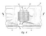
- an integrated circuit die 20is mounted to a lead frame 5 , usually by an adhesive. Bonding pads 26 on the die are connected by bonding wires 28 to respective terminals 30 on the lead frame 5 .
- the lead frame 5 and die 20are then encapsulated by cover 7 to protect the die 20 and the bonding wires 28 .
- the encapsulated lead frame and diethus constitute a first level of packaging.
- the encapsulated die and lead frameare mounted to a printed circuit board to create the second level of packaging.
- the lead framemay be mounted to the printed circuit board by way of solder reflow techniques or through the use of a socket mounted to the printed circuit board which is designed to receive the leads of the lead frame.
- FIG. 2shows a conventional die 20 mounted directly to the circuit board 10 and secured thereto by suitable means such as by an adhesive.
- the die 20has a set of bonding pads 26 which are located on one surface of the die 20 .
- the die 20may be mounted with the bonding pads 26 of the die facing away from the surface of the circuit board 10 to which the die 20 is mounted.
- COBchip-on-board
- FIG. 3shows a die 20 ′ mounted directly to a substrate, such as circuit board 10 .
- the die 20 ′has a set of bonding pads 26 ′ which are located on the bottom surface of the die 20 ′.
- the die 20 ′may be mounted with the bonding pads 26 ′ of the die 20 ′ facing the surface of a substrate such as the printed circuit board 10 ′ to which the die 20 ′ is being mounted.
- This type of arrangementis commonly referred to as flip chip.
- the glob top 46serves as a chemical insulator protecting the die 20 ′ from humidity, oxidation and other harmful elements.
- the glob top 46also protects the die 20 ′ mechanically and relieves mechanical stress in the die 20 ′.
- the invention of the present applicationstacks multiple die on top of one another.
- the stacked diemay or may not be partially or fully recessed into a first recess formed in a first surface of a substrate, such as a circuit board.
- the first recessmay have a stepped cross-section to accommodate die of various sizes.
- An aperturemay be formed in the first recess, extending through the substrate for allowing wire bonding to a second surface of the substrate.
- a first die which is spaced relatively interiorly of a second diemay be wire bonded through the aperture to terminals located on the second surface of the substrate.
- the second diemay be wire bonded to terminals located on the first surface of the substrate.
- a second recessis formed in the second surface of the substrate.
- the terminalsare located within the recessed portion of the second surface.
- Stacking multiple die on a single substratewill greatly increase the space available on the circuit board for the addition of other components. Mounting the die in a recess formed in the substrate will reduce the thickness of the resulting microelectronics package. Fabricating a set of terminals on a surface opposed to the surface on which the die is mounted can shorten the lengths of the bonding wires which connect the die to the substrate. Locating a set of terminals in a second recess formed in the second surface of the substrate will also reduce the thickness of the package and further shorten the length of the bonding wires.
- FIG. 1is a perspective view of a die mounted in a lead frame in a conventional manner.
- FIG. 2is a cross-sectional view of a die mounted on a circuit board in a chip-on-board arrangement.
- FIG. 3is a conventional die mounted on a circuit board in a chip-on-board arrangement.
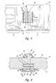
- FIG. 4is a top plan view of an exemplary embodiment of the invention.
- FIG. 5is a bottom plan view of an exemplary embodiment of the invention wherein a pair of die are in stacked arrangement mounted fully-recessed in the circuit board.
- FIG. 6is a cross-sectional view taken along section line 6 of the exemplary embodiment of FIG. 4 .
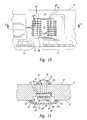
- FIG. 7is a bottom plan view of an exemplary embodiment of the invention wherein a lead-over-chip die is stacked interiorly of a conventional die.
- FIG. 8is a cross-sectional view taken along section line 8 of the exemplary embodiment of FIG. 7 .
- FIG. 9is a cross-sectional view of an alternative exemplary embodiment of the invention wherein a lead-over-chip die is stacked interiorly of a conventional die which is mounted to the circuit board in a flip chip arrangement.
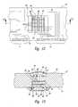
- FIG. 10is a bottom plan view of an exemplary embodiment of the present invention wherein a lead-over-chip die is stacked interiorly of an conventional die.
- FIG. 11is a cross-sectional view taken along section line 11 of the exemplary embodiment of FIG. 10 .
- FIG. 12is a top plan view of an exemplary embodiment of the invention wherein a recess is formed in the second surface of the circuit board and the terminals are located within the recess.
- FIG. 13is a cross-sectional view taken along section line 13 of the exemplary embodiment of FIG. 12 .
- FIG. 14is a cross-sectional view of an additional exemplary embodiment of the invention wherein the inner die is mounted on the surface of the circuit board in flip chip arrangement.
- a first exemplary embodiment of the invention including a pair of lead-over-chip (LOC) die in a stacked arrangementwill be discussed with reference to FIGS. 4-6.
- LOClead-over-chip
- a substrateis shown formed as a circuit board 10 having a first surface 12 .
- a plurality of contacts 14 and conductive traces 16are formed on the first surface 12 of the circuit board 10 .
- the contacts 14permit electrical connections to be made to other circuit leads.
- the conductive traces 16provide electrical connections to various devices located on the circuit board 10 .
- a recess 18is formed in the first surface 12 of the circuit board 10 .
- the recess 18is dimensioned for receiving a pair of die in a stacked arrangement.
- a first or outer die 20is shown mounted in the recess 18 .
- the first die 20has a bottom surface 24 which has a set of bonding pads 26 fabricated thereon.
- bonding padsrefers to any electrical contact formed on a microelectronic device by any method presently known or developed in the future.
- a set of bonding wires 28electrically connect the bonding pads 26 to terminals 30 located on the first surface 12 of the circuit board 10 .
- the circuit board 10has a second surface 32 opposed to the first surface 12 .
- An aperture 34is formed in the first recess 18 and extends through the circuit board 10 .
- the aperture 34is dimensioned for receiving a set of bonding wires 36 therethrough.
- the bonding wires 36electrically connect a set of bonding pads 38 formed on a bottom surface 40 of a second die 42 to a set of terminals 44 formed on the second surface 32 of the circuit board 10 .
- terminalsas used in this specification, refer to any electrical contact formed on a substrate by any method known or developed in the future.
- the first or outer die 20is shown stacked on the second or inner die 42 such that a top surface 50 of the outer die 20 is adjacent a top surface 48 of the inner die 42 .
- the outer die 20 and the inner die 42may be secured to each other prior to being mounted in the first recess 18 .
- the inner die 42may be securely mounted in the recess 18 , and then the outer die 20 may be securely fastened to the inner die 42 .
- the outer and inner die 20 , 42may be fastened to each other or to the circuit board by way of an adhesive (not shown). Double sided non-conducting adhesive tape may be used for securing the die or conducting epoxy, non-conducting epoxy or solder paste may be used. Even where a layer of adhesive exists between the surfaces of the die, the die are considered adjacent within the meaning of the term adjacent as used herein.
- FIG. 7An exemplary embodiment of the invention wherein a LOC die and conventional die are in stacked arrangement will be discussed with reference to FIGS. 7 and 8.
- an outer die 20 ′in the form of a conventional die, is shown mounted in the recess 18 ′ that is dimensioned to receive a pair of die having different sizes.
- the conventional die 20 ′has a set of bonding pads 26 ′ located on a bottom surface 24 of the die 20 ′ and spaced about a periphery thereof.
- a set of bonding wires 28 ′are shown extending between bonding pads 26 ′ and a set of terminals 30 located on the first surface 12 of the circuit board 10 .
- the first recess 18 ′is shown to have a stepped cross section.
- the first recess 18 ′is dimensioned to receive the smaller LOC die, inner die 42 , in the inner portion of the stepped recess 18 ′.
- the first recess 18 ′is further dimensioned to receive the larger conventional die, outer die 20 ′, in the outer portion of the stepped recess 18 ′.
- a set of bonding wires 36electrically connect the inner die 42 to a set of terminals 44 located on the second surface 32 of the circuit board 10 .
- the outer die 20 ′may be mounted in flip chip arrangement, the bonding pads 26 on the outer die 20 ′ in direct contact with terminals 30 located in the stepped portion of the first recess 18 ′.
- FIGS. 10 and 11An exemplary embodiment of the invention wherein a LOC die and a conventional die of a smaller size than the conventional die discussed immediately above will now be discussed with reference to FIGS. 10 and 11.
- the small conventional dieserves as outer die 20 ′′ and is stacked on the relatively larger LOC die which serves as the inner die 42 .
- the fabrication of this embodimentis very similar to that of the exemplary embodiment of FIGS. 7 and 8, however, the bonding wires 28 ′′ extending between the bonding pads 26 ′ of the outer die 20 ′′ and the terminals 30 of the first surface 12 of the substrate, circuit board 10 , are longer than the bonding wires 28 ′ of the prior embodiment.
- the diedo not need to completely fill the recess 18 ′.
- the glob top 46will maintain the position of the die 20 ′′ in the recess 18 ′, as well as, protect the die 20 ′′ from chemical, mechanical and electro-magnetic factors.
- FIGS. 12 and 13A further exemplary embodiment is shown in FIGS. 12 and 13. Again a LOC die serves as the inner die 42 . While a conventional die is shown as serving as the outer die 20 , a second LOC die could be substituted for the conventional die.
- the second surface 32 of the circuit board 10has a second recess 52 formed therein. The second recess 52 is dimensioned for receiving a set of terminals 44 ′ and a set of bonding wires 36 ′ therein. The terminals 44 ′ are located within the second recess 52 .
- the bonding wires 36 ′extend between the terminals 44 ′ and the bonding pads 38 of the inner die 42 .
- the loops of the bonding wires 36 ′are recessed with respect to the second surface 32 of the substrate, shown as circuit board 10 .
- a glob top 46is applied over the second recess 52 .
- FIG. 14An additional exemplary embodiment is shown in FIG. 14 .
- the inner die 42is mounted in a flip chip arrangement on the circuit board 10 such that the bonding pads 38 of the inner die 42 are in direct contact with the terminals 44 ′ located on the first surface 12 of the circuit board 10 .
- the outer die 20is mounted to the inner die 42 , bonding wires 28 extending from the bonding pads 26 of the outer die 20 to a set of terminals 30 located on the first surface 12 of the circuit board 10 .
- the diedo not have to be mounted flush with the substrate surface and may be either recessed from the surface of the substrate or extend partially above the surface, although flush or recess mounting will minimize the thickness of the resulting microelectronics package. Therefore, the particular geometry of the recess and aperture should not be construed to unduly limit the apparatus and methods which accomplish the purpose of mounting the die in stacked relation on the substrate.
- the structure and method taught in accordance with the present inventioncan be applied to other geometry die and die arrangements. Indeed, numerous variations are well within the scope of the invention. Accordingly, the scope of the invention is not limited by the disclosure of particular embodiments, and terms used in the following claims should not be construed to limit the invention to these embodiments. Instead, the scope of the invention is determined entirely by the following claims.
Landscapes
- Engineering & Computer Science (AREA)
- Microelectronics & Electronic Packaging (AREA)
- Power Engineering (AREA)
- Physics & Mathematics (AREA)
- Condensed Matter Physics & Semiconductors (AREA)
- General Physics & Mathematics (AREA)
- Computer Hardware Design (AREA)
- Wire Bonding (AREA)
Abstract
Description
Claims (27)
Priority Applications (1)
| Application Number | Priority Date | Filing Date | Title |
|---|---|---|---|
| US09/545,250US6343019B1 (en) | 1997-12-22 | 2000-04-07 | Apparatus and method of stacking die on a substrate |
Applications Claiming Priority (2)
| Application Number | Priority Date | Filing Date | Title |
|---|---|---|---|
| US99537797A | 1997-12-22 | 1997-12-22 | |
| US09/545,250US6343019B1 (en) | 1997-12-22 | 2000-04-07 | Apparatus and method of stacking die on a substrate |
Related Parent Applications (1)
| Application Number | Title | Priority Date | Filing Date |
|---|---|---|---|
| US99537797AContinuation | 1997-12-22 | 1997-12-22 |
Publications (1)
| Publication Number | Publication Date |
|---|---|
| US6343019B1true US6343019B1 (en) | 2002-01-29 |
Family
ID=25541713
Family Applications (1)
| Application Number | Title | Priority Date | Filing Date |
|---|---|---|---|
| US09/545,250Expired - LifetimeUS6343019B1 (en) | 1997-12-22 | 2000-04-07 | Apparatus and method of stacking die on a substrate |
Country Status (1)
| Country | Link |
|---|---|
| US (1) | US6343019B1 (en) |
Cited By (93)
| Publication number | Priority date | Publication date | Assignee | Title |
|---|---|---|---|---|
| US20020043709A1 (en)* | 2000-10-13 | 2002-04-18 | Yeh Nai Hua | Stackable integrated circuit |
| US6472736B1 (en)* | 2002-03-13 | 2002-10-29 | Kingpak Technology Inc. | Stacked structure for memory chips |
| US6518655B2 (en)* | 2000-10-16 | 2003-02-11 | Oki Electric Industry Co., Ltd. | Multi-chip package-type semiconductor device |
| US20030064542A1 (en)* | 2001-10-02 | 2003-04-03 | Corisis David J. | Methods of packaging an integrated circuit |
| US20030197284A1 (en)* | 2002-02-21 | 2003-10-23 | United Test & Assembly Center Limited | Semiconductor package |
| US20040009631A1 (en)* | 2002-07-10 | 2004-01-15 | Mike Connell | Semiconductor package with circuit side polymer layer and wafer level fabrication method |
| US6682955B2 (en) | 2002-05-08 | 2004-01-27 | Micron Technology, Inc. | Stacked die module and techniques for forming a stacked die module |
| US20040047349A1 (en)* | 2002-08-20 | 2004-03-11 | Nec Corporation | Packet transfer equipment, packet transfer method resolution server, DNS server, network system and program |
| US6731009B1 (en)* | 2000-03-20 | 2004-05-04 | Cypress Semiconductor Corporation | Multi-die assembly |
| US20040095736A1 (en)* | 2002-11-18 | 2004-05-20 | Samsung Electronics Co., Ltd. | Multi-chip package having increased reliabilty |
| US20040106229A1 (en)* | 2002-06-27 | 2004-06-03 | Tongbi Jiang | Methods for assembling multiple semiconductor devices |
| US20040155360A1 (en)* | 1999-09-02 | 2004-08-12 | Salman Akram | Board-on-chip packages |
| US6791184B2 (en)* | 2002-07-23 | 2004-09-14 | Hewlett-Packard Development Company, L.P. | Support assembly for an integrated circuit package having solder columns |
| US20040207060A1 (en)* | 1999-02-19 | 2004-10-21 | Corisis David J. | Integrated circuit packages, ball-grid array integrated circuit packages and methods of packaging an integrated circuit |
| US20040217459A1 (en)* | 2001-03-30 | 2004-11-04 | Fee Setho Sing | Ball grid array interposer, packages and methods |
| US20050218518A1 (en)* | 2002-01-07 | 2005-10-06 | Tongbi Jiang | Semiconductor device assemblies and packages including multiple semiconductor device components |
| US20060261498A1 (en)* | 2005-05-17 | 2006-11-23 | Micron Technology, Inc. | Methods and apparatuses for encapsulating microelectronic devices |
| SG127684A1 (en)* | 2002-08-19 | 2006-12-29 | Micron Technology Inc | Packaged microelectronic component assemblies |
| US20070058471A1 (en)* | 2005-09-02 | 2007-03-15 | Rajan Suresh N | Methods and apparatus of stacking DRAMs |
| US20070085685A1 (en)* | 2005-10-18 | 2007-04-19 | Rf Identics, Inc. | Label with electronic components and method of making same |
| US20070153823A1 (en)* | 2005-12-30 | 2007-07-05 | Jaroslaw Wojtowicz | Small form factor, pluggable ONU |
| US20070192563A1 (en)* | 2006-02-09 | 2007-08-16 | Rajan Suresh N | System and method for translating an address associated with a command communicated between a system and memory circuits |
| US20070204075A1 (en)* | 2006-02-09 | 2007-08-30 | Rajan Suresh N | System and method for reducing command scheduling constraints of memory circuits |
| US20080027703A1 (en)* | 2006-07-31 | 2008-01-31 | Metaram, Inc. | Memory circuit simulation system and method with refresh capabilities |
| US20080028137A1 (en)* | 2006-07-31 | 2008-01-31 | Schakel Keith R | Method and Apparatus For Refresh Management of Memory Modules |
| US20080025136A1 (en)* | 2006-07-31 | 2008-01-31 | Metaram, Inc. | System and method for storing at least a portion of information received in association with a first operation for use in performing a second operation |
| US20080028136A1 (en)* | 2006-07-31 | 2008-01-31 | Schakel Keith R | Method and apparatus for refresh management of memory modules |
| US20080094805A1 (en)* | 2004-11-26 | 2008-04-24 | Imbera Electroics Oy | Electronics Module and Method for Manufacturing the Same |
| US20080115006A1 (en)* | 2006-07-31 | 2008-05-15 | Michael John Sebastian Smith | System and method for adjusting the timing of signals associated with a memory system |
| US20080117056A1 (en)* | 2006-11-22 | 2008-05-22 | Forster Ian J | RFID label with release liner window, and method of making |
| US20080126690A1 (en)* | 2006-02-09 | 2008-05-29 | Rajan Suresh N | Memory module with memory stack |
| US20080133825A1 (en)* | 2006-07-31 | 2008-06-05 | Suresh Natarajan Rajan | System and method for simulating an aspect of a memory circuit |
| US20080137278A1 (en)* | 2006-12-11 | 2008-06-12 | Kreton Corporation | Memory chip and insert card having the same thereon |
| US20080206930A1 (en)* | 2007-02-23 | 2008-08-28 | Micron Technology, Inc. | Systems and methods for compressing an encapsulant adjacent a semiconductor workpiece |
| US20080205008A1 (en)* | 2007-02-23 | 2008-08-28 | Ming Sun | Low Profile Flip Chip Power Module and Method of Making |
| US20090024790A1 (en)* | 2006-07-31 | 2009-01-22 | Suresh Natarajan Rajan | Memory circuit system and method |
| US20090039493A1 (en)* | 2007-08-08 | 2009-02-12 | Phoenix Precision Technology Corporation | Packaging substrate and application thereof |
| US20090087181A1 (en)* | 2007-10-01 | 2009-04-02 | Teknovus | In-wall optical network unit |
| US20090115049A1 (en)* | 2007-11-06 | 2009-05-07 | Shinko Electric Industries Co., Ltd. | Semiconductor package |
| US20090216939A1 (en)* | 2008-02-21 | 2009-08-27 | Smith Michael J S | Emulation of abstracted DIMMs using abstracted DRAMs |
| US20090223701A1 (en)* | 2005-06-27 | 2009-09-10 | Sumitomo Electric Industries, Ltd. | Porous resin base, method for manufacturing same, and multilayer substrate |
| US20100078812A1 (en)* | 2008-09-30 | 2010-04-01 | Chin-Ti Chen | Window bga semiconductor package |
| US20100281280A1 (en)* | 2006-07-31 | 2010-11-04 | Google Inc. | Interface Circuit System And Method For Performing Power Management Operations In Conjunction With Only A Portion Of A Memory Circuit |
| US20100314149A1 (en)* | 2009-06-10 | 2010-12-16 | Medtronic, Inc. | Hermetically-sealed electrical circuit apparatus |
| US8080874B1 (en)* | 2007-09-14 | 2011-12-20 | Google Inc. | Providing additional space between an integrated circuit and a circuit board for positioning a component therebetween |
| US8111566B1 (en) | 2007-11-16 | 2012-02-07 | Google, Inc. | Optimal channel design for memory devices for providing a high-speed memory interface |
| US8130560B1 (en) | 2006-11-13 | 2012-03-06 | Google Inc. | Multi-rank partial width memory modules |
| US8254155B1 (en) | 2011-10-03 | 2012-08-28 | Invensas Corporation | Stub minimization for multi-die wirebond assemblies with orthogonal windows |
| US8345441B1 (en) | 2011-10-03 | 2013-01-01 | Invensas Corporation | Stub minimization for multi-die wirebond assemblies with parallel windows |
| US8370566B2 (en) | 2006-10-05 | 2013-02-05 | Google Inc. | System and method for increasing capacity, performance, and flexibility of flash storage |
| US8386722B1 (en) | 2008-06-23 | 2013-02-26 | Google Inc. | Stacked DIMM memory interface |
| US8386833B2 (en) | 2005-06-24 | 2013-02-26 | Google Inc. | Memory systems and memory modules |
| US8397013B1 (en) | 2006-10-05 | 2013-03-12 | Google Inc. | Hybrid memory module |
| US8405207B1 (en) | 2011-10-03 | 2013-03-26 | Invensas Corporation | Stub minimization for wirebond assemblies without windows |
| US8407412B2 (en) | 2006-07-31 | 2013-03-26 | Google Inc. | Power management of memory circuits by virtual memory simulation |
| US8424388B2 (en) | 2011-01-28 | 2013-04-23 | Medtronic, Inc. | Implantable capacitive pressure sensor apparatus and methods regarding same |
| US8436477B2 (en) | 2011-10-03 | 2013-05-07 | Invensas Corporation | Stub minimization using duplicate sets of signal terminals in assemblies without wirebonds to package substrate |
| US8441111B2 (en) | 2011-10-03 | 2013-05-14 | Invensas Corporation | Stub minimization for multi-die wirebond assemblies with parallel windows |
| US8502390B2 (en) | 2011-07-12 | 2013-08-06 | Tessera, Inc. | De-skewed multi-die packages |
| US8513817B2 (en) | 2011-07-12 | 2013-08-20 | Invensas Corporation | Memory module in a package |
| US8513813B2 (en) | 2011-10-03 | 2013-08-20 | Invensas Corporation | Stub minimization using duplicate sets of terminals for wirebond assemblies without windows |
| US8525327B2 (en) | 2011-10-03 | 2013-09-03 | Invensas Corporation | Stub minimization for assemblies without wirebonds to package substrate |
| US8566556B2 (en) | 2006-02-09 | 2013-10-22 | Google Inc. | Memory module with memory stack and interface with enhanced capabilities |
| US8595419B2 (en) | 2006-07-31 | 2013-11-26 | Google Inc. | Memory apparatus operable to perform a power-saving operation |
| US8666505B2 (en) | 2010-10-26 | 2014-03-04 | Medtronic, Inc. | Wafer-scale package including power source |
| US8670261B2 (en) | 2011-10-03 | 2014-03-11 | Invensas Corporation | Stub minimization using duplicate sets of signal terminals |
| US8705240B1 (en) | 2007-12-18 | 2014-04-22 | Google Inc. | Embossed heat spreader |
| US8773937B2 (en) | 2005-06-24 | 2014-07-08 | Google Inc. | Memory refresh apparatus and method |
| US8787034B2 (en) | 2012-08-27 | 2014-07-22 | Invensas Corporation | Co-support system and microelectronic assembly |
| US8796830B1 (en) | 2006-09-01 | 2014-08-05 | Google Inc. | Stackable low-profile lead frame package |
| US8819356B2 (en) | 2008-07-25 | 2014-08-26 | Google Inc. | Configurable multirank memory system with interface circuit |
| US8823165B2 (en) | 2011-07-12 | 2014-09-02 | Invensas Corporation | Memory module in a package |
| US8848392B2 (en) | 2012-08-27 | 2014-09-30 | Invensas Corporation | Co-support module and microelectronic assembly |
| US8848391B2 (en) | 2012-08-27 | 2014-09-30 | Invensas Corporation | Co-support component and microelectronic assembly |
| US8917532B2 (en) | 2011-10-03 | 2014-12-23 | Invensas Corporation | Stub minimization with terminal grids offset from center of package |
| US8949519B2 (en) | 2005-06-24 | 2015-02-03 | Google Inc. | Simulating a memory circuit |
| US8981547B2 (en) | 2011-10-03 | 2015-03-17 | Invensas Corporation | Stub minimization for multi-die wirebond assemblies with parallel windows |
| US9070423B2 (en) | 2013-06-11 | 2015-06-30 | Invensas Corporation | Single package dual channel memory with co-support |
| US9123555B2 (en) | 2013-10-25 | 2015-09-01 | Invensas Corporation | Co-support for XFD packaging |
| US9171585B2 (en) | 2005-06-24 | 2015-10-27 | Google Inc. | Configurable memory circuit system and method |
| US9281296B2 (en) | 2014-07-31 | 2016-03-08 | Invensas Corporation | Die stacking techniques in BGA memory package for small footprint CPU and memory motherboard design |
| US9368477B2 (en) | 2012-08-27 | 2016-06-14 | Invensas Corporation | Co-support circuit panel and microelectronic packages |
| US20160190048A1 (en)* | 2011-04-21 | 2016-06-30 | Tessera, Inc. | Stacked chip-on-board module with edge connector |
| US9484080B1 (en) | 2015-11-09 | 2016-11-01 | Invensas Corporation | High-bandwidth memory application with controlled impedance loading |
| US9507739B2 (en) | 2005-06-24 | 2016-11-29 | Google Inc. | Configurable memory circuit system and method |
| US9640515B2 (en) | 2011-04-21 | 2017-05-02 | Tessera, Inc. | Multiple die stacking for two or more die |
| US9679613B1 (en) | 2016-05-06 | 2017-06-13 | Invensas Corporation | TFD I/O partition for high-speed, high-density applications |
| US9691437B2 (en) | 2014-09-25 | 2017-06-27 | Invensas Corporation | Compact microelectronic assembly having reduced spacing between controller and memory packages |
| US9711434B2 (en)* | 2015-09-17 | 2017-07-18 | Semiconductor Components Industries, Llc | Stacked semiconductor device structure and method |
| US9806017B2 (en) | 2011-04-21 | 2017-10-31 | Tessera, Inc. | Flip-chip, face-up and face-down centerbond memory wirebond assemblies |
| US10013371B2 (en) | 2005-06-24 | 2018-07-03 | Google Llc | Configurable memory circuit system and method |
| US20190019756A1 (en)* | 2016-07-20 | 2019-01-17 | Taiwan Semiconductor Manufacturing Company, Ltd. | System on integrated chips and methods of forming the same |
| WO2024032023A1 (en)* | 2022-08-08 | 2024-02-15 | 长鑫存储技术有限公司 | Package structure and preparation method therefor |
Citations (14)
| Publication number | Priority date | Publication date | Assignee | Title |
|---|---|---|---|---|
| EP0231937A2 (en) | 1986-02-06 | 1987-08-12 | Hitachi Maxell Ltd. | An arrangement of a semiconductor device for use in a card |
| EP0595549A2 (en) | 1992-10-26 | 1994-05-04 | Hughes Microelectronics Europa Limited | Radio frequency baggage tags |
| US5412538A (en)* | 1993-07-19 | 1995-05-02 | Cordata, Inc. | Space-saving memory module |
| US5528222A (en) | 1994-09-09 | 1996-06-18 | International Business Machines Corporation | Radio frequency circuit and memory in thin flexible package |
| US5566441A (en) | 1993-03-11 | 1996-10-22 | British Technology Group Limited | Attaching an electronic circuit to a substrate |
| US5600175A (en) | 1994-07-27 | 1997-02-04 | Texas Instruments Incorporated | Apparatus and method for flat circuit assembly |
| US5652462A (en)* | 1993-04-05 | 1997-07-29 | Matsushita Electric Industrial Co., Ltd. | Multilevel semiconductor integrated circuit device |
| US5661339A (en)* | 1992-09-16 | 1997-08-26 | Clayton; James E. | Thin multichip module |
| US5682143A (en) | 1994-09-09 | 1997-10-28 | International Business Machines Corporation | Radio frequency identification tag |
| US5696395A (en)* | 1991-12-20 | 1997-12-09 | Industrial Technology Research Institute | Dynamic random access memory with fin-type stacked capacitor |
| US5754408A (en)* | 1995-11-29 | 1998-05-19 | Mitsubishi Semiconductor America, Inc. | Stackable double-density integrated circuit assemblies |
| US5818698A (en)* | 1995-10-12 | 1998-10-06 | Micron Technology, Inc. | Method and apparatus for a chip-on-board semiconductor module |
| US5875100A (en)* | 1996-05-31 | 1999-02-23 | Nec Corporation | High-density mounting method and structure for electronic circuit board |
| US5998860A (en)* | 1997-12-19 | 1999-12-07 | Texas Instruments Incorporated | Double sided single inline memory module |
- 2000
- 2000-04-07USUS09/545,250patent/US6343019B1/ennot_activeExpired - Lifetime
Patent Citations (15)
| Publication number | Priority date | Publication date | Assignee | Title |
|---|---|---|---|---|
| EP0231937B1 (en) | 1986-02-06 | 1993-12-08 | Hitachi Maxell Ltd. | An arrangement of a semiconductor device for use in a card |
| EP0231937A2 (en) | 1986-02-06 | 1987-08-12 | Hitachi Maxell Ltd. | An arrangement of a semiconductor device for use in a card |
| US5696395A (en)* | 1991-12-20 | 1997-12-09 | Industrial Technology Research Institute | Dynamic random access memory with fin-type stacked capacitor |
| US5661339A (en)* | 1992-09-16 | 1997-08-26 | Clayton; James E. | Thin multichip module |
| EP0595549A2 (en) | 1992-10-26 | 1994-05-04 | Hughes Microelectronics Europa Limited | Radio frequency baggage tags |
| US5566441A (en) | 1993-03-11 | 1996-10-22 | British Technology Group Limited | Attaching an electronic circuit to a substrate |
| US5652462A (en)* | 1993-04-05 | 1997-07-29 | Matsushita Electric Industrial Co., Ltd. | Multilevel semiconductor integrated circuit device |
| US5412538A (en)* | 1993-07-19 | 1995-05-02 | Cordata, Inc. | Space-saving memory module |
| US5600175A (en) | 1994-07-27 | 1997-02-04 | Texas Instruments Incorporated | Apparatus and method for flat circuit assembly |
| US5682143A (en) | 1994-09-09 | 1997-10-28 | International Business Machines Corporation | Radio frequency identification tag |
| US5528222A (en) | 1994-09-09 | 1996-06-18 | International Business Machines Corporation | Radio frequency circuit and memory in thin flexible package |
| US5818698A (en)* | 1995-10-12 | 1998-10-06 | Micron Technology, Inc. | Method and apparatus for a chip-on-board semiconductor module |
| US5754408A (en)* | 1995-11-29 | 1998-05-19 | Mitsubishi Semiconductor America, Inc. | Stackable double-density integrated circuit assemblies |
| US5875100A (en)* | 1996-05-31 | 1999-02-23 | Nec Corporation | High-density mounting method and structure for electronic circuit board |
| US5998860A (en)* | 1997-12-19 | 1999-12-07 | Texas Instruments Incorporated | Double sided single inline memory module |
Cited By (220)
| Publication number | Priority date | Publication date | Assignee | Title |
|---|---|---|---|---|
| US6939739B2 (en) | 1999-02-19 | 2005-09-06 | Micron Technology, Inc. | Integrated circuit packages, ball-grid array integrated circuit packages and methods of packaging an integrated circuit |
| US6856013B1 (en) | 1999-02-19 | 2005-02-15 | Micron Technology, Inc. | Integrated circuit packages, ball-grid array integrated circuit packages and methods of packaging an integrated circuit |
| US20040207060A1 (en)* | 1999-02-19 | 2004-10-21 | Corisis David J. | Integrated circuit packages, ball-grid array integrated circuit packages and methods of packaging an integrated circuit |
| US6917107B2 (en) | 1999-09-02 | 2005-07-12 | Micron Technology, Inc. | Board-on-chip packages |
| US20040155360A1 (en)* | 1999-09-02 | 2004-08-12 | Salman Akram | Board-on-chip packages |
| US7443022B2 (en) | 1999-09-02 | 2008-10-28 | Micron Technology, Inc. | Board-on-chip packages |
| US6825550B2 (en) | 1999-09-02 | 2004-11-30 | Micron Technology, Inc. | Board-on-chip packages with conductive foil on the chip surface |
| US6900077B2 (en)* | 1999-09-02 | 2005-05-31 | Micron Technology, Inc. | Methods of forming board-on-chip packages |
| US6731009B1 (en)* | 2000-03-20 | 2004-05-04 | Cypress Semiconductor Corporation | Multi-die assembly |
| US20020043709A1 (en)* | 2000-10-13 | 2002-04-18 | Yeh Nai Hua | Stackable integrated circuit |
| US6518655B2 (en)* | 2000-10-16 | 2003-02-11 | Oki Electric Industry Co., Ltd. | Multi-chip package-type semiconductor device |
| US7274095B2 (en) | 2001-03-30 | 2007-09-25 | Micron Technology, Inc. | Interposers with receptacles for receiving semiconductor devices and assemblies and packages including such interposers |
| US7528007B2 (en) | 2001-03-30 | 2009-05-05 | Micron Technology, Inc. | Methods for assembling semiconductor devices and interposers |
| US20040217459A1 (en)* | 2001-03-30 | 2004-11-04 | Fee Setho Sing | Ball grid array interposer, packages and methods |
| US20030064542A1 (en)* | 2001-10-02 | 2003-04-03 | Corisis David J. | Methods of packaging an integrated circuit |
| US20050218518A1 (en)* | 2002-01-07 | 2005-10-06 | Tongbi Jiang | Semiconductor device assemblies and packages including multiple semiconductor device components |
| SG121705A1 (en)* | 2002-02-21 | 2006-05-26 | United Test & Assembly Ct Ltd | Semiconductor package |
| US20030197284A1 (en)* | 2002-02-21 | 2003-10-23 | United Test & Assembly Center Limited | Semiconductor package |
| US8288862B2 (en)* | 2002-02-21 | 2012-10-16 | United Test & Assembly Center Limited | Multiple die stack package |
| US6472736B1 (en)* | 2002-03-13 | 2002-10-29 | Kingpak Technology Inc. | Stacked structure for memory chips |
| US7029931B2 (en) | 2002-05-08 | 2006-04-18 | Micron Technology, Inc. | Stacked die module and techniques for forming a stacked die module |
| US7186576B2 (en) | 2002-05-08 | 2007-03-06 | Micron Technology, Inc. | Stacked die module and techniques for forming a stacked die module |
| US7755204B2 (en) | 2002-05-08 | 2010-07-13 | Micron Technology, Inc. | Stacked die module including multiple adhesives that cure at different temperatures |
| US7217596B2 (en) | 2002-05-08 | 2007-05-15 | Micron Technology, Inc. | Stacked die module and techniques for forming a stacked die module |
| US20040154722A1 (en)* | 2002-05-08 | 2004-08-12 | Cobbley Chad A. | Stacked die module and techniques for forming a stacked die module |
| US20040157373A1 (en)* | 2002-05-08 | 2004-08-12 | Cobbley Chad A. | Stacked die module and techniques for forming a stacked die module |
| US20040155327A1 (en)* | 2002-05-08 | 2004-08-12 | Cobbley Chad A. | Stacked die module and techniques for forming a stacked die module |
| US6682955B2 (en) | 2002-05-08 | 2004-01-27 | Micron Technology, Inc. | Stacked die module and techniques for forming a stacked die module |
| US20040154956A1 (en)* | 2002-05-08 | 2004-08-12 | Cobbley Chad A. | Stacked die module and techniques for forming a stacked die module |
| US20040056342A1 (en)* | 2002-05-08 | 2004-03-25 | Cobbley Chad A. | Stacked die module and techniques for forming a stacked die module |
| US20060063283A1 (en)* | 2002-05-08 | 2006-03-23 | Cobbley Chad A | Stacked die module and techniques for forming a stacked die module |
| US7198980B2 (en)* | 2002-06-27 | 2007-04-03 | Micron Technology, Inc. | Methods for assembling multiple semiconductor devices |
| US20040106229A1 (en)* | 2002-06-27 | 2004-06-03 | Tongbi Jiang | Methods for assembling multiple semiconductor devices |
| US7573136B2 (en) | 2002-06-27 | 2009-08-11 | Micron Technology, Inc. | Semiconductor device assemblies and packages including multiple semiconductor device components |
| US6949834B2 (en) | 2002-07-10 | 2005-09-27 | Micron Technology, Inc. | Stacked semiconductor package with circuit side polymer layer |
| US6995041B2 (en) | 2002-07-10 | 2006-02-07 | Micron Technology, Inc. | Semiconductor package with circuit side polymer layer and wafer level fabrication method |
| US7479413B2 (en) | 2002-07-10 | 2009-01-20 | Micron Technology, Inc. | Method for fabricating semiconductor package with circuit side polymer layer |
| US20060292752A1 (en)* | 2002-07-10 | 2006-12-28 | Mike Connell | Method for fabricating board on chip (BOC) semiconductor package with circuit side polymer layer |
| US7537966B2 (en) | 2002-07-10 | 2009-05-26 | Micron Technology, Inc. | Method for fabricating board on chip (BOC) semiconductor package with circuit side polymer layer |
| US20040171191A1 (en)* | 2002-07-10 | 2004-09-02 | Mike Connell | Stacked semiconductor package with circuit side polymer layer |
| US6791168B1 (en) | 2002-07-10 | 2004-09-14 | Micron Technology, Inc. | Semiconductor package with circuit side polymer layer and wafer level fabrication method |
| US20040009631A1 (en)* | 2002-07-10 | 2004-01-15 | Mike Connell | Semiconductor package with circuit side polymer layer and wafer level fabrication method |
| US6791184B2 (en)* | 2002-07-23 | 2004-09-14 | Hewlett-Packard Development Company, L.P. | Support assembly for an integrated circuit package having solder columns |
| SG127684A1 (en)* | 2002-08-19 | 2006-12-29 | Micron Technology Inc | Packaged microelectronic component assemblies |
| US20040047349A1 (en)* | 2002-08-20 | 2004-03-11 | Nec Corporation | Packet transfer equipment, packet transfer method resolution server, DNS server, network system and program |
| US20040095736A1 (en)* | 2002-11-18 | 2004-05-20 | Samsung Electronics Co., Ltd. | Multi-chip package having increased reliabilty |
| US20080094805A1 (en)* | 2004-11-26 | 2008-04-24 | Imbera Electroics Oy | Electronics Module and Method for Manufacturing the Same |
| US8547701B2 (en) | 2004-11-26 | 2013-10-01 | Imbera Electronics Oy | Electronics module and method for manufacturing the same |
| US20060261498A1 (en)* | 2005-05-17 | 2006-11-23 | Micron Technology, Inc. | Methods and apparatuses for encapsulating microelectronic devices |
| US8615679B2 (en) | 2005-06-24 | 2013-12-24 | Google Inc. | Memory modules with reliability and serviceability functions |
| US8949519B2 (en) | 2005-06-24 | 2015-02-03 | Google Inc. | Simulating a memory circuit |
| US8773937B2 (en) | 2005-06-24 | 2014-07-08 | Google Inc. | Memory refresh apparatus and method |
| US8359187B2 (en) | 2005-06-24 | 2013-01-22 | Google Inc. | Simulating a different number of memory circuit devices |
| US20080027702A1 (en)* | 2005-06-24 | 2008-01-31 | Metaram, Inc. | System and method for simulating a different number of memory circuits |
| US9507739B2 (en) | 2005-06-24 | 2016-11-29 | Google Inc. | Configurable memory circuit system and method |
| US9171585B2 (en) | 2005-06-24 | 2015-10-27 | Google Inc. | Configurable memory circuit system and method |
| US8386833B2 (en) | 2005-06-24 | 2013-02-26 | Google Inc. | Memory systems and memory modules |
| US10013371B2 (en) | 2005-06-24 | 2018-07-03 | Google Llc | Configurable memory circuit system and method |
| US20090223701A1 (en)* | 2005-06-27 | 2009-09-10 | Sumitomo Electric Industries, Ltd. | Porous resin base, method for manufacturing same, and multilayer substrate |
| US8619452B2 (en) | 2005-09-02 | 2013-12-31 | Google Inc. | Methods and apparatus of stacking DRAMs |
| US8213205B2 (en) | 2005-09-02 | 2012-07-03 | Google Inc. | Memory system including multiple memory stacks |
| US20070058471A1 (en)* | 2005-09-02 | 2007-03-15 | Rajan Suresh N | Methods and apparatus of stacking DRAMs |
| US8811065B2 (en) | 2005-09-02 | 2014-08-19 | Google Inc. | Performing error detection on DRAMs |
| US8582339B2 (en) | 2005-09-02 | 2013-11-12 | Google Inc. | System including memory stacks |
| US20100020585A1 (en)* | 2005-09-02 | 2010-01-28 | Rajan Suresh N | Methods and apparatus of stacking drams |
| US20070085685A1 (en)* | 2005-10-18 | 2007-04-19 | Rf Identics, Inc. | Label with electronic components and method of making same |
| US20070188332A1 (en)* | 2005-10-18 | 2007-08-16 | Peter Phaneuf | Label with electronic components and method of making same |
| US7843341B2 (en) | 2005-10-18 | 2010-11-30 | Avery Dennison Corporation | Label with electronic components and method of making same |
| US7224278B2 (en) | 2005-10-18 | 2007-05-29 | Avery Dennison Corporation | Label with electronic components and method of making same |
| US20070153823A1 (en)* | 2005-12-30 | 2007-07-05 | Jaroslaw Wojtowicz | Small form factor, pluggable ONU |
| US7693178B2 (en)* | 2005-12-30 | 2010-04-06 | Teknovus, Inc. | Small form factor, pluggable ONU |
| US9727458B2 (en) | 2006-02-09 | 2017-08-08 | Google Inc. | Translating an address associated with a command communicated between a system and memory circuits |
| US8566556B2 (en) | 2006-02-09 | 2013-10-22 | Google Inc. | Memory module with memory stack and interface with enhanced capabilities |
| US8797779B2 (en) | 2006-02-09 | 2014-08-05 | Google Inc. | Memory module with memory stack and interface with enhanced capabilites |
| US20070204075A1 (en)* | 2006-02-09 | 2007-08-30 | Rajan Suresh N | System and method for reducing command scheduling constraints of memory circuits |
| US20080120443A1 (en)* | 2006-02-09 | 2008-05-22 | Suresh Natarajan Rajan | System and method for reducing command scheduling constraints of memory circuits |
| US20070192563A1 (en)* | 2006-02-09 | 2007-08-16 | Rajan Suresh N | System and method for translating an address associated with a command communicated between a system and memory circuits |
| US20080126690A1 (en)* | 2006-02-09 | 2008-05-29 | Rajan Suresh N | Memory module with memory stack |
| US9542352B2 (en) | 2006-02-09 | 2017-01-10 | Google Inc. | System and method for reducing command scheduling constraints of memory circuits |
| US9632929B2 (en) | 2006-02-09 | 2017-04-25 | Google Inc. | Translating an address associated with a command communicated between a system and memory circuits |
| US9542353B2 (en) | 2006-02-09 | 2017-01-10 | Google Inc. | System and method for reducing command scheduling constraints of memory circuits |
| US20080109598A1 (en)* | 2006-07-31 | 2008-05-08 | Schakel Keith R | Method and apparatus for refresh management of memory modules |
| US20080123459A1 (en)* | 2006-07-31 | 2008-05-29 | Metaram, Inc. | Combined signal delay and power saving system and method for use with a plurality of memory circuits |
| US20100281280A1 (en)* | 2006-07-31 | 2010-11-04 | Google Inc. | Interface Circuit System And Method For Performing Power Management Operations In Conjunction With Only A Portion Of A Memory Circuit |
| US8972673B2 (en) | 2006-07-31 | 2015-03-03 | Google Inc. | Power management of memory circuits by virtual memory simulation |
| US9047976B2 (en) | 2006-07-31 | 2015-06-02 | Google Inc. | Combined signal delay and power saving for use with a plurality of memory circuits |
| US20080027703A1 (en)* | 2006-07-31 | 2008-01-31 | Metaram, Inc. | Memory circuit simulation system and method with refresh capabilities |
| US20090024790A1 (en)* | 2006-07-31 | 2009-01-22 | Suresh Natarajan Rajan | Memory circuit system and method |
| US8112266B2 (en) | 2006-07-31 | 2012-02-07 | Google Inc. | Apparatus for simulating an aspect of a memory circuit |
| US8745321B2 (en) | 2006-07-31 | 2014-06-03 | Google Inc. | Simulating a memory standard |
| US8671244B2 (en) | 2006-07-31 | 2014-03-11 | Google Inc. | Simulating a memory standard |
| US8667312B2 (en) | 2006-07-31 | 2014-03-04 | Google Inc. | Performing power management operations |
| US8181048B2 (en) | 2006-07-31 | 2012-05-15 | Google Inc. | Performing power management operations |
| US20080133825A1 (en)* | 2006-07-31 | 2008-06-05 | Suresh Natarajan Rajan | System and method for simulating an aspect of a memory circuit |
| US8244971B2 (en) | 2006-07-31 | 2012-08-14 | Google Inc. | Memory circuit system and method |
| US8631220B2 (en) | 2006-07-31 | 2014-01-14 | Google Inc. | Adjusting the timing of signals associated with a memory system |
| US8868829B2 (en) | 2006-07-31 | 2014-10-21 | Google Inc. | Memory circuit system and method |
| US8280714B2 (en) | 2006-07-31 | 2012-10-02 | Google Inc. | Memory circuit simulation system and method with refresh capabilities |
| US20080115006A1 (en)* | 2006-07-31 | 2008-05-15 | Michael John Sebastian Smith | System and method for adjusting the timing of signals associated with a memory system |
| US8407412B2 (en) | 2006-07-31 | 2013-03-26 | Google Inc. | Power management of memory circuits by virtual memory simulation |
| US8327104B2 (en) | 2006-07-31 | 2012-12-04 | Google Inc. | Adjusting the timing of signals associated with a memory system |
| US8340953B2 (en) | 2006-07-31 | 2012-12-25 | Google, Inc. | Memory circuit simulation with power saving capabilities |
| US8601204B2 (en) | 2006-07-31 | 2013-12-03 | Google Inc. | Simulating a refresh operation latency |
| US20080028136A1 (en)* | 2006-07-31 | 2008-01-31 | Schakel Keith R | Method and apparatus for refresh management of memory modules |
| US8595419B2 (en) | 2006-07-31 | 2013-11-26 | Google Inc. | Memory apparatus operable to perform a power-saving operation |
| US20080025136A1 (en)* | 2006-07-31 | 2008-01-31 | Metaram, Inc. | System and method for storing at least a portion of information received in association with a first operation for use in performing a second operation |
| US20080027697A1 (en)* | 2006-07-31 | 2008-01-31 | Metaram, Inc. | Memory circuit simulation system and method with power saving capabilities |
| US8566516B2 (en) | 2006-07-31 | 2013-10-22 | Google Inc. | Refresh management of memory modules |
| US20080028137A1 (en)* | 2006-07-31 | 2008-01-31 | Schakel Keith R | Method and Apparatus For Refresh Management of Memory Modules |
| US8796830B1 (en) | 2006-09-01 | 2014-08-05 | Google Inc. | Stackable low-profile lead frame package |
| US8977806B1 (en) | 2006-10-05 | 2015-03-10 | Google Inc. | Hybrid memory module |
| US8751732B2 (en) | 2006-10-05 | 2014-06-10 | Google Inc. | System and method for increasing capacity, performance, and flexibility of flash storage |
| US8370566B2 (en) | 2006-10-05 | 2013-02-05 | Google Inc. | System and method for increasing capacity, performance, and flexibility of flash storage |
| US8397013B1 (en) | 2006-10-05 | 2013-03-12 | Google Inc. | Hybrid memory module |
| US8760936B1 (en) | 2006-11-13 | 2014-06-24 | Google Inc. | Multi-rank partial width memory modules |
| US8130560B1 (en) | 2006-11-13 | 2012-03-06 | Google Inc. | Multi-rank partial width memory modules |
| US8446781B1 (en) | 2006-11-13 | 2013-05-21 | Google Inc. | Multi-rank partial width memory modules |
| US7701352B2 (en) | 2006-11-22 | 2010-04-20 | Avery Dennison Corporation | RFID label with release liner window, and method of making |
| US20080117056A1 (en)* | 2006-11-22 | 2008-05-22 | Forster Ian J | RFID label with release liner window, and method of making |
| US20080137278A1 (en)* | 2006-12-11 | 2008-06-12 | Kreton Corporation | Memory chip and insert card having the same thereon |
| US20080205008A1 (en)* | 2007-02-23 | 2008-08-28 | Ming Sun | Low Profile Flip Chip Power Module and Method of Making |
| US20080206930A1 (en)* | 2007-02-23 | 2008-08-28 | Micron Technology, Inc. | Systems and methods for compressing an encapsulant adjacent a semiconductor workpiece |
| US7833456B2 (en) | 2007-02-23 | 2010-11-16 | Micron Technology, Inc. | Systems and methods for compressing an encapsulant adjacent a semiconductor workpiece |
| US8159828B2 (en)* | 2007-02-23 | 2012-04-17 | Alpha & Omega Semiconductor, Inc. | Low profile flip chip power module and method of making |
| US20090039493A1 (en)* | 2007-08-08 | 2009-02-12 | Phoenix Precision Technology Corporation | Packaging substrate and application thereof |
| US8080874B1 (en)* | 2007-09-14 | 2011-12-20 | Google Inc. | Providing additional space between an integrated circuit and a circuit board for positioning a component therebetween |
| US20090087181A1 (en)* | 2007-10-01 | 2009-04-02 | Teknovus | In-wall optical network unit |
| US8155526B2 (en) | 2007-10-01 | 2012-04-10 | Broadcom Corporation | In-wall optical network unit |
| US20090115049A1 (en)* | 2007-11-06 | 2009-05-07 | Shinko Electric Industries Co., Ltd. | Semiconductor package |
| US7960820B2 (en)* | 2007-11-06 | 2011-06-14 | Shinko Electric Industries Co., Ltd. | Semiconductor package |
| US8111566B1 (en) | 2007-11-16 | 2012-02-07 | Google, Inc. | Optimal channel design for memory devices for providing a high-speed memory interface |
| US8675429B1 (en) | 2007-11-16 | 2014-03-18 | Google Inc. | Optimal channel design for memory devices for providing a high-speed memory interface |
| US8730670B1 (en) | 2007-12-18 | 2014-05-20 | Google Inc. | Embossed heat spreader |
| US8705240B1 (en) | 2007-12-18 | 2014-04-22 | Google Inc. | Embossed heat spreader |
| US8631193B2 (en) | 2008-02-21 | 2014-01-14 | Google Inc. | Emulation of abstracted DIMMS using abstracted DRAMS |
| US20090216939A1 (en)* | 2008-02-21 | 2009-08-27 | Smith Michael J S | Emulation of abstracted DIMMs using abstracted DRAMs |
| US8438328B2 (en) | 2008-02-21 | 2013-05-07 | Google Inc. | Emulation of abstracted DIMMs using abstracted DRAMs |
| US8762675B2 (en) | 2008-06-23 | 2014-06-24 | Google Inc. | Memory system for synchronous data transmission |
| US8386722B1 (en) | 2008-06-23 | 2013-02-26 | Google Inc. | Stacked DIMM memory interface |
| US8819356B2 (en) | 2008-07-25 | 2014-08-26 | Google Inc. | Configurable multirank memory system with interface circuit |
| US20100078812A1 (en)* | 2008-09-30 | 2010-04-01 | Chin-Ti Chen | Window bga semiconductor package |
| US7786568B2 (en)* | 2008-09-30 | 2010-08-31 | Powertech Technology Inc. | Window BGA semiconductor package |
| US8389331B2 (en) | 2009-06-10 | 2013-03-05 | Medtronic, Inc. | Apparatus for restricting moisture ingress |
| US20100314149A1 (en)* | 2009-06-10 | 2010-12-16 | Medtronic, Inc. | Hermetically-sealed electrical circuit apparatus |
| US8263436B2 (en) | 2009-06-10 | 2012-09-11 | Medtronic, Inc. | Apparatus for restricting moisture ingress |
| US8666505B2 (en) | 2010-10-26 | 2014-03-04 | Medtronic, Inc. | Wafer-scale package including power source |
| US9431312B2 (en) | 2010-10-26 | 2016-08-30 | Medtronic, Inc. | Wafer-scale package including power source |
| US9318400B2 (en) | 2010-10-26 | 2016-04-19 | Medtronic, Inc. | Wafer-scale package including power source |
| US8424388B2 (en) | 2011-01-28 | 2013-04-23 | Medtronic, Inc. | Implantable capacitive pressure sensor apparatus and methods regarding same |
| US9806017B2 (en) | 2011-04-21 | 2017-10-31 | Tessera, Inc. | Flip-chip, face-up and face-down centerbond memory wirebond assemblies |
| US20160190048A1 (en)* | 2011-04-21 | 2016-06-30 | Tessera, Inc. | Stacked chip-on-board module with edge connector |
| US9735093B2 (en)* | 2011-04-21 | 2017-08-15 | Tessera, Inc. | Stacked chip-on-board module with edge connector |
| US10622289B2 (en)* | 2011-04-21 | 2020-04-14 | Tessera, Inc. | Stacked chip-on-board module with edge connector |
| US9640515B2 (en) | 2011-04-21 | 2017-05-02 | Tessera, Inc. | Multiple die stacking for two or more die |
| US8759982B2 (en) | 2011-07-12 | 2014-06-24 | Tessera, Inc. | Deskewed multi-die packages |
| US8513817B2 (en) | 2011-07-12 | 2013-08-20 | Invensas Corporation | Memory module in a package |
| US9287216B2 (en) | 2011-07-12 | 2016-03-15 | Invensas Corporation | Memory module in a package |
| US9508629B2 (en) | 2011-07-12 | 2016-11-29 | Invensas Corporation | Memory module in a package |
| US8502390B2 (en) | 2011-07-12 | 2013-08-06 | Tessera, Inc. | De-skewed multi-die packages |
| US8823165B2 (en) | 2011-07-12 | 2014-09-02 | Invensas Corporation | Memory module in a package |
| US8278764B1 (en) | 2011-10-03 | 2012-10-02 | Invensas Corporation | Stub minimization for multi-die wirebond assemblies with orthogonal windows |
| US8254155B1 (en) | 2011-10-03 | 2012-08-28 | Invensas Corporation | Stub minimization for multi-die wirebond assemblies with orthogonal windows |
| US8917532B2 (en) | 2011-10-03 | 2014-12-23 | Invensas Corporation | Stub minimization with terminal grids offset from center of package |
| US8345441B1 (en) | 2011-10-03 | 2013-01-01 | Invensas Corporation | Stub minimization for multi-die wirebond assemblies with parallel windows |
| US8405207B1 (en) | 2011-10-03 | 2013-03-26 | Invensas Corporation | Stub minimization for wirebond assemblies without windows |
| US20130082394A1 (en)* | 2011-10-03 | 2013-04-04 | Invensas Corporation | Stub minimization for multi-die wirebond assemblies with parallel windows |
| US8981547B2 (en) | 2011-10-03 | 2015-03-17 | Invensas Corporation | Stub minimization for multi-die wirebond assemblies with parallel windows |
| US8525327B2 (en) | 2011-10-03 | 2013-09-03 | Invensas Corporation | Stub minimization for assemblies without wirebonds to package substrate |
| US8610260B2 (en) | 2011-10-03 | 2013-12-17 | Invensas Corporation | Stub minimization for assemblies without wirebonds to package substrate |
| US10090280B2 (en) | 2011-10-03 | 2018-10-02 | Invensas Corporation | Microelectronic package including microelectronic elements having stub minimization for wirebond assemblies without windows |
| US8513813B2 (en) | 2011-10-03 | 2013-08-20 | Invensas Corporation | Stub minimization using duplicate sets of terminals for wirebond assemblies without windows |
| US9214455B2 (en) | 2011-10-03 | 2015-12-15 | Invensas Corporation | Stub minimization with terminal grids offset from center of package |
| US9224431B2 (en) | 2011-10-03 | 2015-12-29 | Invensas Corporation | Stub minimization using duplicate sets of signal terminals |
| US9281271B2 (en) | 2011-10-03 | 2016-03-08 | Invensas Corporation | Stub minimization using duplicate sets of signal terminals having modulo-x symmetry in assemblies without wirebonds to package substrate |
| US10032752B2 (en) | 2011-10-03 | 2018-07-24 | Invensas Corporation | Microelectronic package having stub minimization using symmetrically-positioned duplicate sets of terminals for wirebond assemblies without windows |
| US9287195B2 (en) | 2011-10-03 | 2016-03-15 | Invensas Corporation | Stub minimization using duplicate sets of terminals having modulo-x symmetry for wirebond assemblies without windows |
| US9679876B2 (en) | 2011-10-03 | 2017-06-13 | Invensas Corporation | Microelectronic package having at least two microelectronic elements that are horizontally spaced apart from each other |
| US10692842B2 (en) | 2011-10-03 | 2020-06-23 | Invensas Corporation | Microelectronic package including microelectronic elements having stub minimization for wirebond assemblies without windows |
| US8629545B2 (en) | 2011-10-03 | 2014-01-14 | Invensas Corporation | Stub minimization for assemblies without wirebonds to package substrate |
| US10643977B2 (en) | 2011-10-03 | 2020-05-05 | Invensas Corporation | Microelectronic package having stub minimization using symmetrically-positioned duplicate sets of terminals for wirebond assemblies without windows |
| US9373565B2 (en) | 2011-10-03 | 2016-06-21 | Invensas Corporation | Stub minimization for assemblies without wirebonds to package substrate |
| US9377824B2 (en) | 2011-10-03 | 2016-06-28 | Invensas Corporation | Microelectronic assembly including memory packages connected to circuit panel, the memory packages having stub minimization for wirebond assemblies without windows |
| US8653646B2 (en) | 2011-10-03 | 2014-02-18 | Invensas Corporation | Stub minimization using duplicate sets of terminals for wirebond assemblies without windows |
| US9423824B2 (en) | 2011-10-03 | 2016-08-23 | Invensas Corporation | Stub minimization for multi-die wirebond assemblies with parallel windows |
| US8659140B2 (en) | 2011-10-03 | 2014-02-25 | Invensas Corporation | Stub minimization using duplicate sets of signal terminals in assemblies without wirebonds to package substrate |
| US8659139B2 (en) | 2011-10-03 | 2014-02-25 | Invensas Corporation | Stub minimization using duplicate sets of signal terminals in assemblies without wirebonds to package substrate |
| US8436477B2 (en) | 2011-10-03 | 2013-05-07 | Invensas Corporation | Stub minimization using duplicate sets of signal terminals in assemblies without wirebonds to package substrate |
| US9496243B2 (en) | 2011-10-03 | 2016-11-15 | Invensas Corporation | Microelectronic assembly with opposing microelectronic packages each having terminals with signal assignments that mirror each other with respect to a central axis |
| US8659141B2 (en) | 2011-10-03 | 2014-02-25 | Invensas Corporation | Stub minimization using duplicate sets of terminals for wirebond assemblies without windows |
| US8659142B2 (en) | 2011-10-03 | 2014-02-25 | Invensas Corporation | Stub minimization for wirebond assemblies without windows |
| US9515053B2 (en) | 2011-10-03 | 2016-12-06 | Invensas Corporation | Microelectronic packaging without wirebonds to package substrate having terminals with signal assignments that mirror each other with respect to a central axis |
| US9530458B2 (en) | 2011-10-03 | 2016-12-27 | Invensas Corporation | Stub minimization using duplicate sets of signal terminals |
| US8670261B2 (en) | 2011-10-03 | 2014-03-11 | Invensas Corporation | Stub minimization using duplicate sets of signal terminals |
| US8441111B2 (en) | 2011-10-03 | 2013-05-14 | Invensas Corporation | Stub minimization for multi-die wirebond assemblies with parallel windows |
| US8436457B2 (en)* | 2011-10-03 | 2013-05-07 | Invensas Corporation | Stub minimization for multi-die wirebond assemblies with parallel windows |
| US8659143B2 (en) | 2011-10-03 | 2014-02-25 | Invensas Corporation | Stub minimization for wirebond assemblies without windows |
| US9679838B2 (en) | 2011-10-03 | 2017-06-13 | Invensas Corporation | Stub minimization for assemblies without wirebonds to package substrate |
| US8848392B2 (en) | 2012-08-27 | 2014-09-30 | Invensas Corporation | Co-support module and microelectronic assembly |
| US8848391B2 (en) | 2012-08-27 | 2014-09-30 | Invensas Corporation | Co-support component and microelectronic assembly |
| US8787034B2 (en) | 2012-08-27 | 2014-07-22 | Invensas Corporation | Co-support system and microelectronic assembly |
| US9368477B2 (en) | 2012-08-27 | 2016-06-14 | Invensas Corporation | Co-support circuit panel and microelectronic packages |
| US9460758B2 (en) | 2013-06-11 | 2016-10-04 | Invensas Corporation | Single package dual channel memory with co-support |
| US9070423B2 (en) | 2013-06-11 | 2015-06-30 | Invensas Corporation | Single package dual channel memory with co-support |
| US9293444B2 (en) | 2013-10-25 | 2016-03-22 | Invensas Corporation | Co-support for XFD packaging |
| US9123555B2 (en) | 2013-10-25 | 2015-09-01 | Invensas Corporation | Co-support for XFD packaging |
| US9281296B2 (en) | 2014-07-31 | 2016-03-08 | Invensas Corporation | Die stacking techniques in BGA memory package for small footprint CPU and memory motherboard design |
| US9691437B2 (en) | 2014-09-25 | 2017-06-27 | Invensas Corporation | Compact microelectronic assembly having reduced spacing between controller and memory packages |
| US10163772B2 (en) | 2015-09-17 | 2018-12-25 | Semiconductor Components Industries, Llc | Stacked semiconductor device structure and method |
| US9711434B2 (en)* | 2015-09-17 | 2017-07-18 | Semiconductor Components Industries, Llc | Stacked semiconductor device structure and method |
| US10741484B2 (en) | 2015-09-17 | 2020-08-11 | Semiconductor Components Industries, Llc | Stacked semiconductor device structure and method |
| US10026467B2 (en) | 2015-11-09 | 2018-07-17 | Invensas Corporation | High-bandwidth memory application with controlled impedance loading |
| US9484080B1 (en) | 2015-11-09 | 2016-11-01 | Invensas Corporation | High-bandwidth memory application with controlled impedance loading |
| US9928883B2 (en) | 2016-05-06 | 2018-03-27 | Invensas Corporation | TFD I/O partition for high-speed, high-density applications |
| US9679613B1 (en) | 2016-05-06 | 2017-06-13 | Invensas Corporation | TFD I/O partition for high-speed, high-density applications |
| US20190019756A1 (en)* | 2016-07-20 | 2019-01-17 | Taiwan Semiconductor Manufacturing Company, Ltd. | System on integrated chips and methods of forming the same |
| US10332841B2 (en)* | 2016-07-20 | 2019-06-25 | Taiwan Semiconductor Manufacturing Company, Ltd. | System on integrated chips and methods of forming the same |
| TWI717538B (en)* | 2016-07-20 | 2021-02-01 | 台灣積體電路製造股份有限公司 | Semicondcutor device and packaging method |
| US10950553B2 (en) | 2016-07-20 | 2021-03-16 | Taiwan Semiconductor Manufacturing Company, Ltd. | System on integrated chips and methods of forming the same |
| US11532565B2 (en) | 2016-07-20 | 2022-12-20 | Taiwan Semiconductor Manufacturing Co., Ltd. | System on integrated chips and methods of forming the same |
| WO2024032023A1 (en)* | 2022-08-08 | 2024-02-15 | 长鑫存储技术有限公司 | Package structure and preparation method therefor |
Similar Documents
| Publication | Publication Date | Title |
|---|---|---|
| US6343019B1 (en) | Apparatus and method of stacking die on a substrate | |
| US6781240B2 (en) | Semiconductor package with semiconductor chips stacked therein and method of making the package | |
| US5770888A (en) | Integrated chip package with reduced dimensions and leads exposed from the top and bottom of the package | |
| JP3644662B2 (en) | Semiconductor module | |
| US6995448B2 (en) | Semiconductor package including passive elements and method of manufacture | |
| JP2819285B2 (en) | Stacked bottom lead semiconductor package | |
| US20070048903A1 (en) | Multi-chip package type semiconductor device | |
| US20030025199A1 (en) | Super low profile package with stacked dies | |
| US6753599B2 (en) | Semiconductor package and mounting structure on substrate thereof and stack structure thereof | |
| US20080073779A1 (en) | Stacked semiconductor package and method of manufacturing the same | |
| US6791166B1 (en) | Stackable lead frame package using exposed internal lead traces | |
| KR100621547B1 (en) | Multichip Package | |
| KR100391094B1 (en) | Dual die package and manufacturing method thereof | |
| US7154171B1 (en) | Stacking structure for semiconductor devices using a folded over flexible substrate and method therefor | |
| KR100788341B1 (en) | Chip Stacked Semiconductor Packages | |
| JP2524482B2 (en) | QFP structure semiconductor device | |
| US20040125574A1 (en) | Multi-chip semiconductor package and method for manufacturing the same | |
| JP3159950B2 (en) | Socket for mounting semiconductor package | |
| JPH10256473A (en) | Semiconductor device | |
| JP3495566B2 (en) | Semiconductor device | |
| KR100639700B1 (en) | Chip Scale Stacked Chip Packages | |
| KR100708050B1 (en) | Semiconductor Package | |
| KR950003904B1 (en) | Semiconductor package | |
| JP2972486B2 (en) | Semiconductor device | |
| JPH06244313A (en) | Semiconductor package and mounting method |
Legal Events
| Date | Code | Title | Description |
|---|---|---|---|
| FEPP | Fee payment procedure | Free format text:PAYOR NUMBER ASSIGNED (ORIGINAL EVENT CODE: ASPN); ENTITY STATUS OF PATENT OWNER: LARGE ENTITY | |
| STCF | Information on status: patent grant | Free format text:PATENTED CASE | |
| FPAY | Fee payment | Year of fee payment:4 | |
| FPAY | Fee payment | Year of fee payment:8 | |
| FPAY | Fee payment | Year of fee payment:12 | |
| AS | Assignment | Owner name:U.S. BANK NATIONAL ASSOCIATION, AS COLLATERAL AGENT, CALIFORNIA Free format text:SECURITY INTEREST;ASSIGNOR:MICRON TECHNOLOGY, INC.;REEL/FRAME:038669/0001 Effective date:20160426 Owner name:U.S. BANK NATIONAL ASSOCIATION, AS COLLATERAL AGEN Free format text:SECURITY INTEREST;ASSIGNOR:MICRON TECHNOLOGY, INC.;REEL/FRAME:038669/0001 Effective date:20160426 | |
| AS | Assignment | Owner name:MORGAN STANLEY SENIOR FUNDING, INC., AS COLLATERAL AGENT, MARYLAND Free format text:PATENT SECURITY AGREEMENT;ASSIGNOR:MICRON TECHNOLOGY, INC.;REEL/FRAME:038954/0001 Effective date:20160426 Owner name:MORGAN STANLEY SENIOR FUNDING, INC., AS COLLATERAL Free format text:PATENT SECURITY AGREEMENT;ASSIGNOR:MICRON TECHNOLOGY, INC.;REEL/FRAME:038954/0001 Effective date:20160426 | |
| AS | Assignment | Owner name:U.S. BANK NATIONAL ASSOCIATION, AS COLLATERAL AGENT, CALIFORNIA Free format text:CORRECTIVE ASSIGNMENT TO CORRECT THE REPLACE ERRONEOUSLY FILED PATENT #7358718 WITH THE CORRECT PATENT #7358178 PREVIOUSLY RECORDED ON REEL 038669 FRAME 0001. ASSIGNOR(S) HEREBY CONFIRMS THE SECURITY INTEREST;ASSIGNOR:MICRON TECHNOLOGY, INC.;REEL/FRAME:043079/0001 Effective date:20160426 Owner name:U.S. BANK NATIONAL ASSOCIATION, AS COLLATERAL AGEN Free format text:CORRECTIVE ASSIGNMENT TO CORRECT THE REPLACE ERRONEOUSLY FILED PATENT #7358718 WITH THE CORRECT PATENT #7358178 PREVIOUSLY RECORDED ON REEL 038669 FRAME 0001. ASSIGNOR(S) HEREBY CONFIRMS THE SECURITY INTEREST;ASSIGNOR:MICRON TECHNOLOGY, INC.;REEL/FRAME:043079/0001 Effective date:20160426 | |
| AS | Assignment | Owner name:JPMORGAN CHASE BANK, N.A., AS COLLATERAL AGENT, ILLINOIS Free format text:SECURITY INTEREST;ASSIGNORS:MICRON TECHNOLOGY, INC.;MICRON SEMICONDUCTOR PRODUCTS, INC.;REEL/FRAME:047540/0001 Effective date:20180703 Owner name:JPMORGAN CHASE BANK, N.A., AS COLLATERAL AGENT, IL Free format text:SECURITY INTEREST;ASSIGNORS:MICRON TECHNOLOGY, INC.;MICRON SEMICONDUCTOR PRODUCTS, INC.;REEL/FRAME:047540/0001 Effective date:20180703 | |
| AS | Assignment | Owner name:MICRON TECHNOLOGY, INC., IDAHO Free format text:RELEASE BY SECURED PARTY;ASSIGNOR:U.S. BANK NATIONAL ASSOCIATION, AS COLLATERAL AGENT;REEL/FRAME:047243/0001 Effective date:20180629 | |
| AS | Assignment | Owner name:MICRON TECHNOLOGY, INC., IDAHO Free format text:RELEASE BY SECURED PARTY;ASSIGNOR:MORGAN STANLEY SENIOR FUNDING, INC., AS COLLATERAL AGENT;REEL/FRAME:050937/0001 Effective date:20190731 | |
| AS | Assignment | Owner name:MICRON TECHNOLOGY, INC., IDAHO Free format text:RELEASE BY SECURED PARTY;ASSIGNOR:JPMORGAN CHASE BANK, N.A., AS COLLATERAL AGENT;REEL/FRAME:051028/0001 Effective date:20190731 Owner name:MICRON SEMICONDUCTOR PRODUCTS, INC., IDAHO Free format text:RELEASE BY SECURED PARTY;ASSIGNOR:JPMORGAN CHASE BANK, N.A., AS COLLATERAL AGENT;REEL/FRAME:051028/0001 Effective date:20190731 |