US6342802B1 - Multi-voltage power-up stable input/output buffer circuit in a disc drive - Google Patents
Multi-voltage power-up stable input/output buffer circuit in a disc driveDownload PDFInfo
- Publication number
- US6342802B1 US6342802B1US09/575,970US57597000AUS6342802B1US 6342802 B1US6342802 B1US 6342802B1US 57597000 AUS57597000 AUS 57597000AUS 6342802 B1US6342802 B1US 6342802B1
- Authority
- US
- United States
- Prior art keywords
- voltage
- core
- input
- buffer
- output
- Prior art date
- Legal status (The legal status is an assumption and is not a legal conclusion. Google has not performed a legal analysis and makes no representation as to the accuracy of the status listed.)
- Expired - Lifetime
Links
Images


Classifications
- H—ELECTRICITY
- H03—ELECTRONIC CIRCUITRY
- H03K—PULSE TECHNIQUE
- H03K17/00—Electronic switching or gating, i.e. not by contact-making and –breaking
- H03K17/22—Modifications for ensuring a predetermined initial state when the supply voltage has been applied
Definitions
- This inventiongenerally relates to input/output (I/O) buffer circuits and more particularly to a multiple voltage I/O buffer that is stable on power up.
- Some advanced integrated circuitshave two distinct voltages present in the IC. There is a core voltage and an I/O voltage. Each is different than the other. These are called mixed voltage integrated circuits. When the two distinct voltages are applied to and removed from the chip, as when applied to a system implementation, they are often applied or removed at differing time points. Additionally, the state of the Input/Output (I/O) buffers is determined by logic in the core of the IC. This means that both voltages must be present, before the state of the output buffer is determinate. Usually, the core voltage will be present at the same time as the I/O voltage. However, in the case where the I/O voltage is present prior to the core voltage, there is a problem. The problem arises because there are certain signals such as a system reset, for instance, that need to be controlled, i.e., made determinate, anytime the I/O voltage is present, regardless of whether a core voltage is present.
- the state of the I/O buffercannot be solely determined by the I/O power, due to a requirement for Test Modes, and on-the-fly configuration of the buffer. Therefore there is a need for a solution in which the I/O buffer state is made determinate whenever an I/O voltage is present in a mixed voltage integrated circuit.
- the present inventionessentially is an integrated circuit particularly useful in a disc drive controller that ensures that the I/O buffers each power up to a known state based off of the I/O voltage.
- the circuitrythen allows the core to determine the state of the I/O buffers only after the core voltage has reached a predetermined acceptable level. This is accomplished by supplying core power to an additional logic which resides within the I/O buffer itself.
- an input to the I/O buffermay be provided which functions as a mode switch from the core logic. This mode switch input controls whether the I/O buffer state is determined by the default mode or by the core logic.
- the first embodimentbasically involves the use of a high active signal from the core to determine when to switch from the Default Mode to the Core Logic Mode.
- the second embodimentbasically involves using a separate level detect signal circuit outside the core that provides a signal to indicate that the Core Voltage is at an acceptable level to control the core logic. The level detect signal then is used to switch between the Default Mode and the Core Logic Mode.
- FIG. 1is a plan view of a disc drive incorporating a preferred embodiment of an integrated circuit in accordance with the present invention.
- FIG. 2is a simplified functional block diagram of the disc drive shown in FIG. 1 .
- FIG. 3is a schematic block diagram of a mixed voltage integrated circuit in accordance with a first preferred embodiment of the present invention.
- FIG. 4is a schematic block diagram of a mixed voltage integrated circuit in accordance with a second preferred embodiment of the present invention.
- FIG. 5is a timing diagram of the various voltages illustrating the timing of the integrated circuit in FIG. 3 .
- FIG. 6is a simplified schematic diagram of the level detect circuit block in the mixed voltage integrated circuit in FIG. 4 .
- FIG. 7is a simplified schematic diagram of the preferred embodiment of the integrated circuit shown in FIG. 3 .
- the disc drive 100constructed in accordance with a preferred embodiment of the present invention is shown in FIG. 1 .
- the disc drive 100includes a base 102 to which various components of the disc drive 100 are mounted.
- a top cover 104shown partially cut away, cooperates with the base 102 to form an internal, sealed environment for the disc drive in a conventional manner.
- the componentsinclude a spindle motor 106 which rotates one or more discs 108 at a constant high speed. Information is written to and read from tracks on the discs 108 through the use of an actuator assembly 110 , which rotates during a seek operation about a bearing shaft assembly 112 positioned adjacent the discs 108 .
- the actuator assembly 110includes a plurality of actuator arms 114 which extend towards the discs 108 , with one or more flexures 116 extending from each of the actuator arms 114 .
- a head 118mounted at the distal end of each of the flexures 116 is a head 118 which includes an air bearing slider enabling the head 118 to fly in close proximity above the corresponding surface of the associated disc 108 .
- the track position of the heads 118is controlled, during a seek operation, through the use of a voice coil motor (VCM) 124 , that typically includes a coil 126 attached to the actuator assembly 110 , as well as one or more permanent magnets 128 that establish a magnetic field in which the coil 126 is immersed.
- VCMvoice coil motor
- the controlled application of current to the coil 126causes magnetic interaction between the permanent magnets 128 and the coil 126 so that the coil 126 moves in accordance with the well-known Lorentz relationship.
- the actuator assembly 110pivots about the bearing shaft assembly 112 , and the heads 118 are caused to move across the surfaces of the discs 108 .
- the spindle motor 106is typically de-energized when the disc drive 100 is not in use for extended periods of time.
- the heads 118are moved over park zones 120 near the inner diameter of the discs 108 when the drive motor is de-energized.
- the heads 118are secured over the park zones 120 through the use of an actuator latch arrangement, which prevents inadvertent rotation of the actuator assembly 110 when the heads are parked.
- a flex assembly 130provides the requisite electrical connection paths for the actuator assembly 110 while allowing pivotal movement of the actuator assembly 110 during operation.
- the flex assemblyincludes a printed circuit board 132 to which head wires (not shown) are connected; the head wires being routed along the actuator arms 114 and the flexures 116 to the heads 118 .
- the printed circuit board 132typically includes circuitry for controlling the write currents applied to the heads 118 during a write operation and a preamplifier for amplifying read signals generated by the heads 118 during a read operation.
- the flex assemblyterminates at a flex bracket 134 for communication through the base deck 102 to a disc drive printed circuit board (not shown) mounted to the bottom side of the disc drive 100 .
- FIG. 2shown therein is a functional block diagram of the disc drive 100 of FIG. 1, generally showing the main functional circuits which are resident on the disc drive printed circuit board and used to control the operation of the disc drive 100 .
- the disc drive 100is shown in FIG. 2 to be operably connected to a host computer 140 in which the disc drive 100 is mounted in a conventional manner. Control communication paths are provided between the host computer 140 and a disc drive microprocessor 142 , the microprocessor 142 generally providing top level communication and control for the disc drive 100 in conjunction with programming for the microprocessor 142 stored in microprocessor memory (MEM) 143 .
- the MEM 143can include random access memory (RAM), read only memory (ROM) and other sources of resident memory for the microprocessor 142 .
- the level detect module 212is powered by the I/O voltage, not the core voltage 206 .
- the level detect module 212provides a “CVGood” signal to the mode switch input 214 to the I/O buffers 204 when the Core Voltage 206 is within a predetermined operating tolerance level.
- a simplified schematic of the level detect circuit 220 in the level detect module 212is shown in FIG. 6 .
- the level detect circuit 220includes a comparator 222 which has its negative input 224 connected to a reference bandgap block 226 .
- the bandgap block 226has its input connected to the I/O voltage line 208 .
- the positive input 228 of the comparator 222is connected between a pair of resistors R 1 and R 2 forming a voltage divider network 230 which is connected to Core Voltage.
- the comparator 222When the voltage (V+) on the positive input 228 is greater than the voltage on the negative input 224 (V bandgap ), the comparator 222 will output a logic 1 on the mode switch input 214 .
- the comparator 222When the V+ is less than V bandgap , the comparator 222 will output a logic 0.
- R 1 and R 2are selected such that the voltage V+ on the positive input 228 of the comparator 222 will be greater than the V bandgap only when the Core voltage is above a predetermined safe operating level.
- the output of the comparator 222if a logic 0, instructs the I/O buffers to be in the Default Mode. If the output of the comparator 222 is a logic 1, the I/O buffers 204 operate in a Core Logic Mode. Thus, whenever the core voltage is below a predetermined value, the comparator 222 outputs a logic 0 and thus the I/O buffers 204 operate in the Default Mode. This ensures that the I/O buffers are in a known, determined state whenever the core voltage is low, such as on a power reset, power down or power up scenario. Only when the core voltage exceeds a predetermined level with the I/O voltage present will the I/O buffers switch from the Default Mode to the Core Logic Mode. The level detect circuit 220 thus also protects the core logic by ensuring that the mode switches back to the Default Mode whenever the Core Voltage falls below the predetermined threshold determined by R 1 /R 2 .
- the second embodimenthas a separate level detect module that connects to the Mode Switch Input of the I/O buffer.
- the mixed voltage integrated circuit 151shown in FIG. 3, includes a core logic module 152 and one or more Input/Output (I/O) buffers 154 .
- the core logic module 152has a mode switch line 156 and I/O buffer control lines 158 connected between the core logic 152 and the I/O buffers 154 .
- the core logic module 152also has a core voltage output line 160 .
- the I/O buffers 154have an I/O output voltage line 162 as well as a number of data output lines 164 .
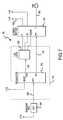
- FIG. 7is a simplified schematic representation of the “power good” sensing portions of the integrated circuit 151 .
- the core logic module 152includes a regulator 300 and the 1.8 volt core logic 302 .
- 1.8 volt poweris generated by the regulator 300 .
- a 3.3 volt supply voltageis connected to the Vdds pin of the voltage regulator 300 .
- the output 308 of a bandgap reference voltage circuit 306is connected via line 308 to the REF pin on the regulator 300 .
- the bandgap reference circuit 306provides a stable reference to the voltage regulator 300 so that it can produce a stable 1.8 volt supply.
- the voltage regulator circuit 300has a “PG” output pin which provides a power good signal on the mode switch line 156 to the I/O buffers 154 . This PG signal is a logical 1 if and only if the core logic voltage (1.8 v) is present and within a safe operating level.
- the regulator circuit 300provides a logical 0 on the mode switch line
- FIG. 5illustrates the timing in the core logic module 152 on the mode switch line 156 upon startup or power-up of the circuit 151 in relation to the I/O voltage, Core Voltage, and System reset signals.
- time t 0no power is applied to the system.
- the I/O buffer outputis maintained low, the mode switch line 156 is low and the I/O voltage line 162 is low.
- the I/O voltagegoes to its nominal voltage, e.g. 3.3 volts, at t 1 .
- the I/O buffer outputsremain low.
- the core voltageis applied and goes to a stable safe operating level, e.g., 1.8 volts.
- the mode switchremains low from t 0 until t 3 .
- the core voltagehas reached a safe operating level, e.g., 1.8 volts, at t 3 .
- the core logicdetermines that all system reset requirements have been met, at time t 4 , the core logic de-asserts the I/O buffer output, i.e., the I/O output goes high and the system is released from reset.
- the integrated circuit 200also includes a core logic module 202 and I/O buffers 204 .
- the core logic 202has a core voltage line 206 which is typically at 1.8 volts and the I/O buffers 204 has an I/O voltage line 208 which is typically at 3.3 volts.
- the I/O buffers 204also have a number of data output lines 210 .
- the mode switch input 214does not run from the core logic module 202 directly to the I/O buffers 204 .
- a level detect circuit module 212is connected between the core voltage line 206 and the I/O voltage output line 208 with its output feeding the mode switch input 214 .
- the output buffersare operated in one of two modes: Default Mode or Core Logic Mode. When both I/O voltage and Core voltage are present, the output buffers are operated in the Core Logic Mode. If not, the output buffers 204 revert to the Default Mode.
- the level detect module 212is powered by the I/O voltage, not the core voltage 206 .
- the level detect module 212provides a “CVGood” signal to the mode switch input 214 to the I/O buffers 204 when the Core Voltage 206 is within a predetermined operating tolerance level.
- a simplified schematic of the level detect circuit 220 in the level detect module 212is shown in FIG. 4 .
- the level detect circuit 220includes a comparator 222 which has its negative input 224 connected to a reference bandgap block 226 .
- the bandgap block 226has its input connected to the I/O voltage line 208 .
- the positive input 228 of the comparator 222is connected between a pair of resistors R 1 and R 2 forming a voltage divider network 230 which is connected to Core Voltage.
- the comparator 222When the voltage (V+) on the positive input 228 is greater than the voltage on the negative input 224 (V bandgap ), the comparator 222 will output a logic 1 on the mode switch input 214 .
- the comparator 222When the V+ is less than V bandgap , the comparator 222 will output a logic 0.
- R 1 and R 2are selected such that the voltage V+ on the positive input 228 of the comparator 222 will be greater than the V bandgap only when the Core voltage is above a predetermined safe operating level.
- the output of the comparator 222if a logic 0, instructs the I/O buffers to be in the Default Mode. If the output of the comparator 222 is a logic 1, the I/O buffers 204 operate in a Core Logic mode. Thus, whenever the core voltage is below a predetermined value, the comparator 222 outputs a logic 0 and thus the I/O buffers 204 operate in the Default mode. This ensures that the I/O buffers are in a known, determined state whenever the core voltage is low, such as on a power reset, power down or power up scenario. Only when the core voltage exceeds a predetermined level with the I/O voltage present will the I/O buffers switch from the Default Mode to the Core Logic Mode. The level detect circuit 220 thus also protects the core logic by ensuring that the mode switches back to the Default Mode whenever the Core Voltage falls below the predetermined threshold determined by R 1 /R 2 .
- the present inventionmay be viewed as an integrated circuit (such as 151 or 200 ) that has a core logic module (such as 152 or 202 ) connected to a core voltage (such as 160 or 206 ), an input/output buffer module (such as 154 or 204 ) connected to an input/output voltage (such as 162 or 208 ), and input/output buffer control lines (such as 158 ) that are connected to the core logic module, and a mode switch input (such as 156 or 214 ) on the I/O buffer module (such as 154 or 204 ).
- the mode switch inputis operable to prevent output operation of the I/O buffers (such as 154 or 204 ) whenever core voltage (such as 160 or 206 ) is below a safe operating level.
- One preferred embodiment(such as 151 ) is configured with the core logic module (such as 152 ) operably connected to the mode switch input (such as 156 ) on the I/O buffer module (such as 154 ).
- the core logic module(such as 152 ) itself determines when the safe operating level is met.
- Another preferred embodimentis configured to have the mode switch input (such as 214 ) connected to a level detect module (such as 212 ) that is operably connected to the core voltage (such as 206 ) and the input/output voltage (such as 208 ).
- the level detect module(such as 212 ) determines when the safe operating level is met in this embodiment.
- the level detect module(such as 212 ) has a comparator (such as 222 ) that compares the core voltage (such as 206 ) to a reference voltage (such as 224 ) to determine the safe operating level.
- This comparator(such as 222 ) preferably has a voltage divider (such as 230 ) connected to the core voltage (such as 206 ) and to a positive input (such as 228 ) of the comparator (such as 222 ).
- An input/output reference voltage(such as 208 ) is connected to a negative input (such as 224 ) of the comparator (such as 222 ).
- the comparatoris powered by the input/output voltage (such as 208 ).
- the present inventionmay be viewed as an integrated circuit (such as 200 ) having an input/output (I/O) buffer (such as 204 ) connected to a core logic module (such as 202 ).
- the core logic modulesuch as 202
- the core logic modulesuch as 202
- the I/O buffersuch as 204
- the I/O bufferis connected to an I/O voltage (such as 208 ).
- a level detect module(such as 212 ) is connected to the core voltage (such as 206 ) and the I/O voltage (such as 208 ) and to a mode switch input (such as 214 ) on the I/O buffer (such as 204 ).
- the level detect module(such as 212 ) is operable to control the I/O buffer (such as 204 ) between a Default Mode preventing I/O buffer output and a Core Logic Mode permitting I/O buffer output from the core logic module (such as 202 ).
- the level detect module(such as 212 ) operates to prevent output of the I/O buffer (such as 204 ) unless the core voltage (such as 206 ) is at a predetermined level.
- the level detect module(such as 212 ) has a comparator (such as 222 ) connected to the I/O voltage (such as 208 ) and has an input (such as 228 ) connected to the core voltage (such as 206 ) through a voltage divider (such as 230 ).
- the comparator(such as 222 ) has another input 15 such as 224 ) connected to a reference voltage (such as 226 ).
- the reference voltage (such as 226 )is connected to the I/O voltage (such as 208 ).
Landscapes
- Semiconductor Integrated Circuits (AREA)
- Logic Circuits (AREA)
- Electronic Switches (AREA)
- Signal Processing For Digital Recording And Reproducing (AREA)
- Power Sources (AREA)
Abstract
Description
Claims (12)
Priority Applications (7)
| Application Number | Priority Date | Filing Date | Title |
|---|---|---|---|
| US09/575,970US6342802B1 (en) | 1999-10-28 | 2000-05-23 | Multi-voltage power-up stable input/output buffer circuit in a disc drive |
| KR1020027005372AKR100747216B1 (en) | 1999-10-28 | 2000-06-26 | Multiple Voltage Supply Stable Input / Output Buffer Circuits for Disk Drives |
| CN00815043ACN1433588A (en) | 1999-10-28 | 2000-06-26 | Mutli-voltage power-up stable input-output buffer circuit in disc drive |
| PCT/US2000/017573WO2001031787A1 (en) | 1999-10-28 | 2000-06-26 | Multi-voltage power-up stable input/output buffer circuit in a disc drive |
| GB0210726AGB2371693B (en) | 1999-10-28 | 2000-06-26 | Multi-voltage power-up stable input/output buffer circuit in a disc drive |
| JP2001533627AJP2003530733A (en) | 1999-10-28 | 2000-06-26 | Input / output buffer circuit stable against multi-voltage power rise of disk drive |
| DE10085146TDE10085146T1 (en) | 1999-10-28 | 2000-06-26 | Multiple voltage, switching power stable input / output pupper circuit in a disk drive |
Applications Claiming Priority (2)
| Application Number | Priority Date | Filing Date | Title |
|---|---|---|---|
| US16227099P | 1999-10-28 | 1999-10-28 | |
| US09/575,970US6342802B1 (en) | 1999-10-28 | 2000-05-23 | Multi-voltage power-up stable input/output buffer circuit in a disc drive |
Publications (1)
| Publication Number | Publication Date |
|---|---|
| US6342802B1true US6342802B1 (en) | 2002-01-29 |
Family
ID=26858598
Family Applications (1)
| Application Number | Title | Priority Date | Filing Date |
|---|---|---|---|
| US09/575,970Expired - LifetimeUS6342802B1 (en) | 1999-10-28 | 2000-05-23 | Multi-voltage power-up stable input/output buffer circuit in a disc drive |
Country Status (7)
| Country | Link |
|---|---|
| US (1) | US6342802B1 (en) |
| JP (1) | JP2003530733A (en) |
| KR (1) | KR100747216B1 (en) |
| CN (1) | CN1433588A (en) |
| DE (1) | DE10085146T1 (en) |
| GB (1) | GB2371693B (en) |
| WO (1) | WO2001031787A1 (en) |
Cited By (16)
| Publication number | Priority date | Publication date | Assignee | Title |
|---|---|---|---|---|
| US6441681B1 (en)* | 2001-06-07 | 2002-08-27 | Texas Instruments Incorporated | Method for preserving charges on a cap at the output of a regulator |
| US6636089B2 (en)* | 2001-04-02 | 2003-10-21 | Stmicroelectronics Sa | Power supply detection device |
| US20040070464A1 (en)* | 2002-05-02 | 2004-04-15 | Wong Keng L. | Voltage control for clock generating circuit |
| US6822479B1 (en) | 2002-05-09 | 2004-11-23 | Marvell Semiconductor Israel Ltd. | I/O buffer power up sequence |
| US20050146355A1 (en)* | 2003-12-29 | 2005-07-07 | Kiyoshi Kase | Level shifter |
| US20070070725A1 (en)* | 2005-09-29 | 2007-03-29 | Hynix Semiconductor Inc. | Internal voltage supplying device |
| US20080158220A1 (en)* | 2007-01-03 | 2008-07-03 | Himax Technologies Limited | Power-on-reset circuit and method therefor |
| US20090096484A1 (en)* | 2007-10-12 | 2009-04-16 | Mediatek Inc. | Level shifters |
| CN102478872A (en)* | 2010-11-29 | 2012-05-30 | 瑞昱半导体股份有限公司 | Electronic device and method |
| CN104218921A (en)* | 2013-05-30 | 2014-12-17 | 长春迪派斯科技有限公司 | Method and device for super-high-speed pulse signal generator |
| WO2015047230A1 (en)* | 2013-09-24 | 2015-04-02 | Intel Corporation | High-voltage tolerant input voltage buffer circuit |
| US9383794B2 (en) | 2014-06-11 | 2016-07-05 | Freescale Semiconductor, Inc. | Integrated circuit with multi-voltage input/output (I/O) cells |
| US11223358B2 (en) | 2020-01-17 | 2022-01-11 | Nxp Usa, Inc. | IO analog rail control circuit for power ramps |
| US11307536B2 (en) | 2015-11-12 | 2022-04-19 | Razer (Asia-Pacific) Pte. Ltd. | Watches |
| US20240201718A1 (en)* | 2022-12-16 | 2024-06-20 | Xilinx, Inc. | Method for implementing an i/o buffer |
| WO2025139154A1 (en)* | 2023-12-28 | 2025-07-03 | 北京四维图新科技股份有限公司 | Voltage detection circuit and electronic device |
Families Citing this family (1)
| Publication number | Priority date | Publication date | Assignee | Title |
|---|---|---|---|---|
| US7830039B2 (en)* | 2007-12-28 | 2010-11-09 | Sandisk Corporation | Systems and circuits with multirange and localized detection of valid power |
Citations (17)
| Publication number | Priority date | Publication date | Assignee | Title |
|---|---|---|---|---|
| US3919568A (en) | 1972-08-01 | 1975-11-11 | Licentia Gmbh | Circuit for the preferential starting of a stage of an electronic sequence having a holding circuit |
| US4142118A (en)* | 1977-08-18 | 1979-02-27 | Mostek Corporation | Integrated circuit with power supply voltage level detection |
| US5300835A (en) | 1993-02-10 | 1994-04-05 | Cirrus Logic, Inc. | CMOS low power mixed voltage bidirectional I/O buffer |
| US5440244A (en) | 1993-02-10 | 1995-08-08 | Cirrus Logic, Inc. | Method and apparatus for controlling a mixed voltage interface in a multivoltage system |
| US5508649A (en)* | 1994-07-21 | 1996-04-16 | National Semiconductor Corporation | Voltage level triggered ESD protection circuit |
| US5537077A (en)* | 1994-12-23 | 1996-07-16 | Advanced Micro Devices, Inc. | Power supply dependent method of controlling a charge pump |
| US5570050A (en)* | 1994-03-08 | 1996-10-29 | Intel Corporation | Zero standby current power-up reset circuit |
| US5737612A (en)* | 1994-09-30 | 1998-04-07 | Cypress Semiconductor Corp. | Power-on reset control circuit |
| US5821787A (en)* | 1994-10-05 | 1998-10-13 | Altera Corporation | Power-on reset circuit with well-defined reassertion voltage |
| US5852370A (en) | 1994-12-22 | 1998-12-22 | Texas Instruments Incorporated | Integrated circuits for low power dissipation in signaling between different-voltage on chip regions |
| US5870617A (en) | 1994-12-22 | 1999-02-09 | Texas Instruments Incorporated | Systems, circuits and methods for mixed voltages and programmable voltage rails on integrated circuits |
| US5900750A (en) | 1997-08-15 | 1999-05-04 | Lsi Logic Corporation | 5V output driver on 2.5V technology |
| US5958026A (en) | 1997-04-11 | 1999-09-28 | Xilinx, Inc. | Input/output buffer supporting multiple I/O standards |
| US5963057A (en) | 1997-08-05 | 1999-10-05 | Lsi Logic Corporation | Chip level bias for buffers driving voltages greater than transistor tolerance |
| US5990730A (en)* | 1998-02-03 | 1999-11-23 | Fujitsu Limited | Semiconductor device with stable operation and reduced power consumption |
| US6028449A (en) | 1997-08-05 | 2000-02-22 | Lsi Logic Corporation | Integrated circuit I/O buffer having pull-up to voltages greater than transistor tolerance |
| US6246272B1 (en)* | 1993-01-29 | 2001-06-12 | Ricoh Company, Ltd. | Power supply voltage detecting apparatus |
Family Cites Families (7)
| Publication number | Priority date | Publication date | Assignee | Title |
|---|---|---|---|---|
| JPS6448556A (en)* | 1987-08-18 | 1989-02-23 | Toshiba Corp | Signal output system |
| JPH0513696A (en)* | 1991-07-03 | 1993-01-22 | Nec Corp | Signal transmission circuit |
| JP3272809B2 (en)* | 1993-05-07 | 2002-04-08 | 株式会社東芝 | Semiconductor integrated circuit device |
| JP3233318B2 (en)* | 1993-11-10 | 2001-11-26 | 日本電信電話株式会社 | Logic circuit |
| JPH07312413A (en)* | 1994-05-17 | 1995-11-28 | Fujitsu Ltd | Output buffer circuit and semiconductor integrated circuit device |
| JPH08106345A (en)* | 1994-10-05 | 1996-04-23 | Fujitsu Ltd | Interface device between different voltage elements |
| JPH09205355A (en)* | 1996-01-29 | 1997-08-05 | Fujitsu Ltd | Semiconductor integrated circuit |
- 2000
- 2000-05-23USUS09/575,970patent/US6342802B1/ennot_activeExpired - Lifetime
- 2000-06-26WOPCT/US2000/017573patent/WO2001031787A1/ennot_activeApplication Discontinuation
- 2000-06-26GBGB0210726Apatent/GB2371693B/ennot_activeExpired - Fee Related
- 2000-06-26KRKR1020027005372Apatent/KR100747216B1/ennot_activeExpired - Fee Related
- 2000-06-26DEDE10085146Tpatent/DE10085146T1/ennot_activeWithdrawn
- 2000-06-26JPJP2001533627Apatent/JP2003530733A/enactivePending
- 2000-06-26CNCN00815043Apatent/CN1433588A/enactivePending
Patent Citations (17)
| Publication number | Priority date | Publication date | Assignee | Title |
|---|---|---|---|---|
| US3919568A (en) | 1972-08-01 | 1975-11-11 | Licentia Gmbh | Circuit for the preferential starting of a stage of an electronic sequence having a holding circuit |
| US4142118A (en)* | 1977-08-18 | 1979-02-27 | Mostek Corporation | Integrated circuit with power supply voltage level detection |
| US6246272B1 (en)* | 1993-01-29 | 2001-06-12 | Ricoh Company, Ltd. | Power supply voltage detecting apparatus |
| US5300835A (en) | 1993-02-10 | 1994-04-05 | Cirrus Logic, Inc. | CMOS low power mixed voltage bidirectional I/O buffer |
| US5440244A (en) | 1993-02-10 | 1995-08-08 | Cirrus Logic, Inc. | Method and apparatus for controlling a mixed voltage interface in a multivoltage system |
| US5570050A (en)* | 1994-03-08 | 1996-10-29 | Intel Corporation | Zero standby current power-up reset circuit |
| US5508649A (en)* | 1994-07-21 | 1996-04-16 | National Semiconductor Corporation | Voltage level triggered ESD protection circuit |
| US5737612A (en)* | 1994-09-30 | 1998-04-07 | Cypress Semiconductor Corp. | Power-on reset control circuit |
| US5821787A (en)* | 1994-10-05 | 1998-10-13 | Altera Corporation | Power-on reset circuit with well-defined reassertion voltage |
| US5852370A (en) | 1994-12-22 | 1998-12-22 | Texas Instruments Incorporated | Integrated circuits for low power dissipation in signaling between different-voltage on chip regions |
| US5870617A (en) | 1994-12-22 | 1999-02-09 | Texas Instruments Incorporated | Systems, circuits and methods for mixed voltages and programmable voltage rails on integrated circuits |
| US5537077A (en)* | 1994-12-23 | 1996-07-16 | Advanced Micro Devices, Inc. | Power supply dependent method of controlling a charge pump |
| US5958026A (en) | 1997-04-11 | 1999-09-28 | Xilinx, Inc. | Input/output buffer supporting multiple I/O standards |
| US5963057A (en) | 1997-08-05 | 1999-10-05 | Lsi Logic Corporation | Chip level bias for buffers driving voltages greater than transistor tolerance |
| US6028449A (en) | 1997-08-05 | 2000-02-22 | Lsi Logic Corporation | Integrated circuit I/O buffer having pull-up to voltages greater than transistor tolerance |
| US5900750A (en) | 1997-08-15 | 1999-05-04 | Lsi Logic Corporation | 5V output driver on 2.5V technology |
| US5990730A (en)* | 1998-02-03 | 1999-11-23 | Fujitsu Limited | Semiconductor device with stable operation and reduced power consumption |
Non-Patent Citations (1)
| Title |
|---|
| Apr. 1989 IBM Technical Disclosure Bulletin, vol. 31, No. 11, pp. 413-416. |
Cited By (26)
| Publication number | Priority date | Publication date | Assignee | Title |
|---|---|---|---|---|
| US6636089B2 (en)* | 2001-04-02 | 2003-10-21 | Stmicroelectronics Sa | Power supply detection device |
| US6441681B1 (en)* | 2001-06-07 | 2002-08-27 | Texas Instruments Incorporated | Method for preserving charges on a cap at the output of a regulator |
| US7242261B2 (en)* | 2002-05-02 | 2007-07-10 | Intel Corporation | Voltage control for clock generating circuit |
| US20040070464A1 (en)* | 2002-05-02 | 2004-04-15 | Wong Keng L. | Voltage control for clock generating circuit |
| US6778033B2 (en)* | 2002-05-02 | 2004-08-17 | Intel Corporation | Voltage control for clock generating circuit |
| US6822479B1 (en) | 2002-05-09 | 2004-11-23 | Marvell Semiconductor Israel Ltd. | I/O buffer power up sequence |
| US20050146355A1 (en)* | 2003-12-29 | 2005-07-07 | Kiyoshi Kase | Level shifter |
| US7002371B2 (en)* | 2003-12-29 | 2006-02-21 | Freescale Semiconductor, Inc. | Level shifter |
| US20100320988A1 (en)* | 2005-09-29 | 2010-12-23 | Chang-Ho Do | Internal voltage supplying device |
| US20070070725A1 (en)* | 2005-09-29 | 2007-03-29 | Hynix Semiconductor Inc. | Internal voltage supplying device |
| US8183912B2 (en) | 2005-09-29 | 2012-05-22 | Hynix Semiconductor Inc. | Internal voltage supplying device |
| US20080158220A1 (en)* | 2007-01-03 | 2008-07-03 | Himax Technologies Limited | Power-on-reset circuit and method therefor |
| US20090096484A1 (en)* | 2007-10-12 | 2009-04-16 | Mediatek Inc. | Level shifters |
| US7804327B2 (en) | 2007-10-12 | 2010-09-28 | Mediatek Inc. | Level shifters |
| CN102478872A (en)* | 2010-11-29 | 2012-05-30 | 瑞昱半导体股份有限公司 | Electronic device and method |
| CN102478872B (en)* | 2010-11-29 | 2014-07-16 | 瑞昱半导体股份有限公司 | Electronic device and method |
| CN104218921B (en)* | 2013-05-30 | 2017-06-06 | 长春迪派斯科技有限公司 | A kind of ultrahigh speed pulse signal generator |
| CN104218921A (en)* | 2013-05-30 | 2014-12-17 | 长春迪派斯科技有限公司 | Method and device for super-high-speed pulse signal generator |
| WO2015047230A1 (en)* | 2013-09-24 | 2015-04-02 | Intel Corporation | High-voltage tolerant input voltage buffer circuit |
| US9608636B2 (en) | 2013-09-24 | 2017-03-28 | Intel Corporation | High-voltage tolerant input voltage buffer circuit |
| US9383794B2 (en) | 2014-06-11 | 2016-07-05 | Freescale Semiconductor, Inc. | Integrated circuit with multi-voltage input/output (I/O) cells |
| US11307536B2 (en) | 2015-11-12 | 2022-04-19 | Razer (Asia-Pacific) Pte. Ltd. | Watches |
| US11223358B2 (en) | 2020-01-17 | 2022-01-11 | Nxp Usa, Inc. | IO analog rail control circuit for power ramps |
| US20240201718A1 (en)* | 2022-12-16 | 2024-06-20 | Xilinx, Inc. | Method for implementing an i/o buffer |
| US12153458B2 (en)* | 2022-12-16 | 2024-11-26 | Xilinx, Inc. | Method for implementing an I/O buffer |
| WO2025139154A1 (en)* | 2023-12-28 | 2025-07-03 | 北京四维图新科技股份有限公司 | Voltage detection circuit and electronic device |
Also Published As
| Publication number | Publication date |
|---|---|
| GB0210726D0 (en) | 2002-06-19 |
| GB2371693B (en) | 2004-01-21 |
| WO2001031787A1 (en) | 2001-05-03 |
| DE10085146T1 (en) | 2003-12-04 |
| JP2003530733A (en) | 2003-10-14 |
| CN1433588A (en) | 2003-07-30 |
| KR20030081001A (en) | 2003-10-17 |
| KR100747216B1 (en) | 2007-08-10 |
| GB2371693A (en) | 2002-07-31 |
Similar Documents
| Publication | Publication Date | Title |
|---|---|---|
| US6342802B1 (en) | Multi-voltage power-up stable input/output buffer circuit in a disc drive | |
| US7023647B2 (en) | Fly height control for a read/write head in a hard disk drive | |
| US7443627B1 (en) | Lowest power mode for a mobile drive | |
| US6622252B1 (en) | Data storage device having selectable performance modes for use in dual powered portable devices | |
| JPH0950350A (en) | Storage device | |
| US6373650B1 (en) | Voice coil motor control circuit having alternative modes of operation and method of operation thereof | |
| US20140160595A1 (en) | Emergency power off (epo) island for saving critical data to non-volatile memory | |
| US6377015B1 (en) | Voice coil motor control apparatus for use in disk drives | |
| US7006314B2 (en) | Magnetic head driver circuit and magnetic storage device | |
| US7373529B2 (en) | Performing a power supply check for an information storage device to increase power consumption in a stepwise manner | |
| US4479154A (en) | Floppy disk drive with local processor control | |
| US7457068B2 (en) | Magnetic disk drive with efficient power generation | |
| US6754028B2 (en) | Control integrated circuit for floppy disk drive | |
| US6624962B1 (en) | Storage device and method in which write/read fault errors are not generated when mode is switched from power save mode or migration mode to ordinary mode | |
| US7092190B2 (en) | Dynamic power supply | |
| US20090059414A1 (en) | Hard disk drive with power saving feature | |
| US20040042109A1 (en) | Power efficient overshoot protection during an operating mode transition | |
| JPH11306501A (en) | Disk unit | |
| US7581123B2 (en) | Recording media drive provided with a connecting pin for supply of 3.3V | |
| US7000067B2 (en) | Virtual expansion of program RAM size | |
| JP2731206B2 (en) | Magnetic disk drive | |
| JP3758931B2 (en) | FDD device | |
| KR100260409B1 (en) | Method and apparatus for minimizing power saving and mode switching time in magnetic disk drive | |
| US6282044B1 (en) | 8V ring clamp circuit | |
| JP2004500674A (en) | Dual mode disk device and method |
Legal Events
| Date | Code | Title | Description |
|---|---|---|---|
| AS | Assignment | Owner name:SEAGATE TECHNOLOGY, INC., CALIFORNIA Free format text:ASSIGNMENT OF ASSIGNORS INTEREST;ASSIGNOR:FOREHAND, MONTY AARON;REEL/FRAME:010860/0715 Effective date:20000515 | |
| AS | Assignment | Owner name:SEAGATE TECHNOLOGY LLC, CALIFORNIA Free format text:ASSIGNMENT OF ASSIGNORS INTEREST;ASSIGNOR:SEAGATE TECHNOLOGY, INC.;REEL/FRAME:010988/0322 Effective date:20000630 | |
| STCF | Information on status: patent grant | Free format text:PATENTED CASE | |
| AS | Assignment | Owner name:JPMORGAN CHASE BANK, AS COLLATERAL AGENT, NEW YORK Free format text:SECURITY AGREEMENT;ASSIGNOR:SEAGATE TECHNOLOGY LLC;REEL/FRAME:013177/0001 Effective date:20020513 Owner name:JPMORGAN CHASE BANK, AS COLLATERAL AGENT,NEW YORK Free format text:SECURITY AGREEMENT;ASSIGNOR:SEAGATE TECHNOLOGY LLC;REEL/FRAME:013177/0001 Effective date:20020513 | |
| CC | Certificate of correction | ||
| CC | Certificate of correction | ||
| FEPP | Fee payment procedure | Free format text:PAYOR NUMBER ASSIGNED (ORIGINAL EVENT CODE: ASPN); ENTITY STATUS OF PATENT OWNER: LARGE ENTITY | |
| FPAY | Fee payment | Year of fee payment:4 | |
| AS | Assignment | Owner name:SEAGATE TECHNOLOGY LLC, CALIFORNIA Free format text:RELEASE OF SECURITY INTERESTS IN PATENT RIGHTS;ASSIGNOR:JPMORGAN CHASE BANK, N.A. (FORMERLY KNOWN AS THE CHASE MANHATTAN BANK AND JPMORGAN CHASE BANK), AS ADMINISTRATIVE AGENT;REEL/FRAME:016958/0294 Effective date:20051130 | |
| AS | Assignment | Owner name:WELLS FARGO BANK, NATIONAL ASSOCIATION, AS COLLATERAL AGENT AND SECOND PRIORITY REPRESENTATIVE, CALIFORNIA Free format text:SECURITY AGREEMENT;ASSIGNORS:MAXTOR CORPORATION;SEAGATE TECHNOLOGY LLC;SEAGATE TECHNOLOGY INTERNATIONAL;REEL/FRAME:022757/0017 Effective date:20090507 Owner name:JPMORGAN CHASE BANK, N.A., AS ADMINISTRATIVE AGENT AND FIRST PRIORITY REPRESENTATIVE, NEW YORK Free format text:SECURITY AGREEMENT;ASSIGNORS:MAXTOR CORPORATION;SEAGATE TECHNOLOGY LLC;SEAGATE TECHNOLOGY INTERNATIONAL;REEL/FRAME:022757/0017 Effective date:20090507 Owner name:JPMORGAN CHASE BANK, N.A., AS ADMINISTRATIVE AGENT Free format text:SECURITY AGREEMENT;ASSIGNORS:MAXTOR CORPORATION;SEAGATE TECHNOLOGY LLC;SEAGATE TECHNOLOGY INTERNATIONAL;REEL/FRAME:022757/0017 Effective date:20090507 Owner name:WELLS FARGO BANK, NATIONAL ASSOCIATION, AS COLLATE Free format text:SECURITY AGREEMENT;ASSIGNORS:MAXTOR CORPORATION;SEAGATE TECHNOLOGY LLC;SEAGATE TECHNOLOGY INTERNATIONAL;REEL/FRAME:022757/0017 Effective date:20090507 | |
| FPAY | Fee payment | Year of fee payment:8 | |
| AS | Assignment | Owner name:SEAGATE TECHNOLOGY HDD HOLDINGS, CALIFORNIA Free format text:RELEASE;ASSIGNOR:JPMORGAN CHASE BANK, N.A., AS ADMINISTRATIVE AGENT;REEL/FRAME:025662/0001 Effective date:20110114 Owner name:SEAGATE TECHNOLOGY LLC, CALIFORNIA Free format text:RELEASE;ASSIGNOR:JPMORGAN CHASE BANK, N.A., AS ADMINISTRATIVE AGENT;REEL/FRAME:025662/0001 Effective date:20110114 Owner name:MAXTOR CORPORATION, CALIFORNIA Free format text:RELEASE;ASSIGNOR:JPMORGAN CHASE BANK, N.A., AS ADMINISTRATIVE AGENT;REEL/FRAME:025662/0001 Effective date:20110114 Owner name:SEAGATE TECHNOLOGY INTERNATIONAL, CALIFORNIA Free format text:RELEASE;ASSIGNOR:JPMORGAN CHASE BANK, N.A., AS ADMINISTRATIVE AGENT;REEL/FRAME:025662/0001 Effective date:20110114 | |
| AS | Assignment | Owner name:THE BANK OF NOVA SCOTIA, AS ADMINISTRATIVE AGENT, CANADA Free format text:SECURITY AGREEMENT;ASSIGNOR:SEAGATE TECHNOLOGY LLC;REEL/FRAME:026010/0350 Effective date:20110118 Owner name:THE BANK OF NOVA SCOTIA, AS ADMINISTRATIVE AGENT, Free format text:SECURITY AGREEMENT;ASSIGNOR:SEAGATE TECHNOLOGY LLC;REEL/FRAME:026010/0350 Effective date:20110118 | |
| FPAY | Fee payment | Year of fee payment:12 | |
| AS | Assignment | Owner name:SEAGATE TECHNOLOGY LLC, CALIFORNIA Free format text:TERMINATION AND RELEASE OF SECURITY INTEREST IN PATENT RIGHTS;ASSIGNOR:WELLS FARGO BANK, NATIONAL ASSOCIATION, AS COLLATERAL AGENT AND SECOND PRIORITY REPRESENTATIVE;REEL/FRAME:030833/0001 Effective date:20130312 Owner name:SEAGATE TECHNOLOGY US HOLDINGS, INC., CALIFORNIA Free format text:TERMINATION AND RELEASE OF SECURITY INTEREST IN PATENT RIGHTS;ASSIGNOR:WELLS FARGO BANK, NATIONAL ASSOCIATION, AS COLLATERAL AGENT AND SECOND PRIORITY REPRESENTATIVE;REEL/FRAME:030833/0001 Effective date:20130312 Owner name:SEAGATE TECHNOLOGY INTERNATIONAL, CAYMAN ISLANDS Free format text:TERMINATION AND RELEASE OF SECURITY INTEREST IN PATENT RIGHTS;ASSIGNOR:WELLS FARGO BANK, NATIONAL ASSOCIATION, AS COLLATERAL AGENT AND SECOND PRIORITY REPRESENTATIVE;REEL/FRAME:030833/0001 Effective date:20130312 Owner name:EVAULT INC. (F/K/A I365 INC.), CALIFORNIA Free format text:TERMINATION AND RELEASE OF SECURITY INTEREST IN PATENT RIGHTS;ASSIGNOR:WELLS FARGO BANK, NATIONAL ASSOCIATION, AS COLLATERAL AGENT AND SECOND PRIORITY REPRESENTATIVE;REEL/FRAME:030833/0001 Effective date:20130312 | |
| AS | Assignment | Owner name:SEAGATE TECHNOLOGY PUBLIC LIMITED COMPANY, CALIFORNIA Free format text:RELEASE BY SECURED PARTY;ASSIGNOR:THE BANK OF NOVA SCOTIA;REEL/FRAME:072193/0001 Effective date:20250303 Owner name:SEAGATE TECHNOLOGY, CALIFORNIA Free format text:RELEASE BY SECURED PARTY;ASSIGNOR:THE BANK OF NOVA SCOTIA;REEL/FRAME:072193/0001 Effective date:20250303 Owner name:SEAGATE TECHNOLOGY HDD HOLDINGS, CALIFORNIA Free format text:RELEASE BY SECURED PARTY;ASSIGNOR:THE BANK OF NOVA SCOTIA;REEL/FRAME:072193/0001 Effective date:20250303 Owner name:I365 INC., CALIFORNIA Free format text:RELEASE BY SECURED PARTY;ASSIGNOR:THE BANK OF NOVA SCOTIA;REEL/FRAME:072193/0001 Effective date:20250303 Owner name:SEAGATE TECHNOLOGY LLC, CALIFORNIA Free format text:RELEASE BY SECURED PARTY;ASSIGNOR:THE BANK OF NOVA SCOTIA;REEL/FRAME:072193/0001 Effective date:20250303 Owner name:SEAGATE TECHNOLOGY INTERNATIONAL, CAYMAN ISLANDS Free format text:RELEASE BY SECURED PARTY;ASSIGNOR:THE BANK OF NOVA SCOTIA;REEL/FRAME:072193/0001 Effective date:20250303 Owner name:SEAGATE HDD CAYMAN, CAYMAN ISLANDS Free format text:RELEASE BY SECURED PARTY;ASSIGNOR:THE BANK OF NOVA SCOTIA;REEL/FRAME:072193/0001 Effective date:20250303 Owner name:SEAGATE TECHNOLOGY (US) HOLDINGS, INC., CALIFORNIA Free format text:RELEASE BY SECURED PARTY;ASSIGNOR:THE BANK OF NOVA SCOTIA;REEL/FRAME:072193/0001 Effective date:20250303 |